
Submitted:
28 March 2025
Posted:
28 March 2025
You are already at the latest version
Abstract
The S-shaped dinaphtho[2,1-b:2′,1′-f] thieno[3,2-b]thiophene (S-DNTT) molecules have shown promise for applications in organic electronic devices, though their molecular characteristics are not yet fully understood. In this study, it firstly revealed the material characteristics of S-DNTT-10 by vibrational dynamics using Raman spectroscopy and density functional theory (DFT) simulations with employing B3LYP functional method and the 6-311G (d, p) basis set. The molecular vibrations identified include C-H bending in alkyl chains and deformation of S-shaped thiophene rings. Additionally, it suggested that surface-enhanced Raman scattering (SERS) with 785 nm incident light was applied to thermally deposited 25 nm S-DNTT-10 thin-films with gold (Au) nanostructures. It illustrated the enhancing Raman signals from the lower S-DNTT-10 layers. The findings significantly contribute to the knowledge of S-DNTT-10 molecular properties and using this material into organic electronic devices in the future.
Keywords:
S-DNTT-10
; Raman scattered
; DFT simulation
; SERS effect
1. Introduction
Due to their unique advantages of organic semiconductor (OSC) materials, making organic electronic device, such as, organic thin-film transistors (OTFTs), possess advantages, such as high flexibility, large-area fabrication compatibility, and lower temperature manufacturing, compared to inorganic counterparts.[1,2,3,4,5,6] These characteristics rendered OTFTs highly promising for integration into commercial organic electronics. To date, OTFTs are successfully used in various applications.[7,8,9,10,11]
In the field of organic thin-film transistors (OTFTs), organic semiconductors (OSCs) play a critical role in determining device performance.[12,13,14,15] Historically, OTFTs have employed OSC layers with relatively simple molecular structures, such as acenes, heteroacenes, and their derivatives.[16,17] However, OTFT development has advanced significantly with the introduction of OSCs featuring larger and more complex molecular architectures.[18,19,20,21,22,23,24,25,26,27] A notable example is the S-shaped dinaphtho[2,1-b:2′,1′-f]thieno[3,2-b]thiophene (S-DNTT) family, particularly S-DNTT-10, as shown in Figure 1, which is characterized by a distinctive S-shaped thiophene core and alkyl chains composed of ten carbon atoms.[28] This molecular structure facilitates efficient charge transport, enabling charge carrier mobilities of several cm2·V-1·s-1 in thermally deposited OTFTs. Moreover, its improved stability under ambient conditions further highlights its suitability for organic electronic applications.[28] Despite its promising performance and growing application prospects, the molecular characteristics of S-DNTT-10 are still not fully understood. Given its considerable potential in organic electronic devices, further investigations are essential to achieve a comprehensive understanding of its molecular properties.
Herein, building upon previous preliminary research,[28] this study aims to investigate the molecular vibrational spectra of S-DNTT-10 using Raman scattering—a well-established, non-destructive technique for probing molecular structures. Initially, the Raman spectrum of S-DNTT-10 was examined by comparing experimentally obtained non-resonant Raman spectra with simulated spectra generated through Density Functional Theory (DFT), providing detailed insights into the molecular vibrational modes. These results bridge the existing knowledge gap regarding the Raman spectral characteristics and vibrational mode analysis of S-DNTT-10. Subsequently, the weak Raman signal of a 25-nm-thick S-DNTT-10 thin film was enhanced by thermally depositing gold (Au) films several nanometers thick, resulting in the formation of Au nanostructures. This enhancement is primarily attributed to surface-enhanced Raman scattering (SERS). The findings suggest that the degree of Raman signal enhancement depends on both the thickness of the deposited Au films and the wavelength of the incident light.
2. Materials and Methods
2.1. Fabrication of S-DNTT-10 Thin-Films
All S-DNTT-10 thin-films were fabricated by PVD (Physical Vapored Deposition) method, on heavily doped p-type Si (100) wafers (0.02 Ω/cm) covered with 99 nm SiO2 dielectric layer. Then cleaned the Si/SiO2 substrate with ultrasonication in acetone, isopropanol, and Milli-Q water for removing contaminants or impurities that possibly degraded the quality of deposited S-DNTT-10. Subsequently, the substrates were stationary in a chemically deposited chamber for approximately 16 hours at room temperature to form approximately a few nanometers of self-assembled monolayer (SAM) layers named HMDS (1,1,1,3,3,3-Hexamethyldisilazane) at the purpose of adjusting the deposited organic molecular arrangement. And then the S-DNTT-10 bulk material (TCI EUROPE N.V., Zwijndrecht, Belgium) were deposited on the Si/SiO2 substrate with surface modification layer HMDS at the defined deposited rate of 0.1 - 0.3 Å·s-1 under the vacuum environment (~ 10-7 Pa) and the room temperature.
2.2. Fabrication of gold (Au) Nanostructures
The Au nanoparticles in this study were thermally deposited as the form of nano-layers on the S-DNTT-10 thin films with a rate of 1.0 Å·s-1 under the room temperature in the vacuum environment (~ 10-7 Pa).
3. Results and Discussion
3.1. Theoretical Calculation and Measured Raman Spectrum
To investigate the Raman spectra of S-DNTT-10, density functional theory (DFT) simulations were performed using the B3LYP functional and the 6-311G (d,p) basis set. The optimized molecular structure is shown in Figure S1, and a summary of the Gaussian calculation parameters is provided in Figure S2. Figure 2 (a) presents the simulated non-resonant Raman spectrum in the 1100–1550 cm-1 range, which displays twelve distinct peaks labeled 1–12. These peaks correspond to specific vibrational modes of the S-DNTT-10 molecule, each associated with unique atomic displacement patterns. For example, modes 1 and 7, illustrated in Figure 2 (c) and 2 (d), respectively, demonstrate the diversity of vibrational behavior. Red arrows indicate atomic displacement directions, with arrow lengths proportional to displacement magnitude. Mode 1 is characterized by C–H bending in the alkyl chains, coupled with deformation of the thiophene rings. In contrast, mode 7 involves significant deformation of the aromatic and thiophene rings, along with C–H bond bending. Detailed descriptions of these modes are summarized in Table 1, offering insights into the vibrational characteristics of S-DNTT-10.
Subsequently, Raman spectroscopy was employed to analyze the experimental Raman spectrum of S-DNTT-10 under 532 nm incident light with an output power of approximately 6.22 mW. Figure 2 (b) presents the Raman spectrum obtained from a 25-nm-thick S-DNTT-10 film. Although certain experimental peaks align closely with the theoretical predictions, notable discrepancies are evident (Figure 2 (a)). For instance, distinct peak splitting observed in vibrational modes 2 and 8 deviated significantly from theoretical predictions. These deviations are likely attributable to Davydov splitting,[29] which arises from differences in intermolecular interactions between adjacent molecules. It is plausible that the molecular arrangement became more disordered during the deposition of the S-DNTT-10 thin film, in contrast to the well-ordered initial deposition of a few molecular layers on the SiO2 substrate. The disparity in molecular orientation, is presumed to contribute to the observed peak splitting in mode 2 and mode 8.
Figure 2(b) presents the non-resonant Raman spectrum of S-DNTT-10, which closely aligns with the simulated spectrum shown in Figure 2 (a). These simulations reveal the vibrational characteristics of S-DNTT-10. The spectral features resemble those of other OSCs, such as DNTT ,[15] as evidenced by variations in peak intensities across different vibrational modes. Based on classical Raman theory, the intensity of Raman scattering is proportional to changes in molecular polarizability. Variations in peak intensity result from fluctuations in polarizability during molecular vibrations. DFT results indicate that these modes primarily involve bending and deformation of molecular bonds. Dynamic structural changes during vibrations modulate the Raman scattering cross-section accordingly. For instance, the peak at ~1373.03 cm-1 (mode 7) exhibits the highest intensity, while mode 1 (~1150 cm-1) shows comparatively lower intensity. According to the analysis summarized in Table 1, mode 7 involves significant C–C stretching within the thiophene rings, coupled with C–H bending. In contrast, mode 1 primarily consists of C–H bending in the alkyl chains, with minor bond stretching.
Figure 2 (b) presents the non-resonant Raman spectrum of S-DNTT-10, closely matching the simulated DFT spectrum shown in Figure 2(a). These simulations provide insights into the vibrational characteristics of S-DNTT-10. However, some discrepancies were observed between the experimental and simulated spectra, similar to previously reported deviations observed for DNTT prior to applying scaling factors.[30,31] These differences likely arise because experimental thin films comprise densely packed molecules, whereas DFT simulations assume isolated molecules.[15] Compared to isolated molecules, densely packed arrangements inherently involve altered intermolecular interactions, modifying electronic distributions and molecular polarizabilities. Consequently, peak positions and intensities in experimental spectra may deviate from theoretical predictions.
These spectral variations originate from intermolecular interactions within the thin-film structure, significantly affecting Raman spectral characteristics. Although DFT simulations provide a valuable theoretical framework for understanding molecular vibrations and associated spectroscopic properties, they do not fully capture the complexities arising from intermolecular interactions present in condensed-phase systems, such as thin films. This limitation underscores the necessity of integrating theoretical predictions with experimental observations to comprehensively characterize Raman spectral properties of organic semiconductors, thus bridging the gap between idealized theoretical models and complex behaviors observed experimentally.
3.2. The SERS Effect on S-DNTT-10 Thin-Film
In the previous section, the Raman spectrum of a 700 nm-thick S-DNTT-10 film was compared with the DFT-simulated spectrum of an isolated S-DNTT-10 molecule. Further investigation, shown in Figure 3, reveals a clear dependence of Raman scattering intensity on the thickness of S-DNTT-10 films. Notably, as film thickness increases, the experimental Raman spectrum progressively approaches the spectral characteristics of powdered S-DNTT-10, exhibiting enhanced spectral clarity and detail. In contrast, significantly thinner films, e.g., a 25 nm S-DNTT-10 film, display fewer discernible vibrational modes, with signals largely obscured by background noise. This observation indicates that thinner films result in reduced detectability of specific Raman modes, highlighting the significant influence of film thickness on Raman signal quality and clarity. Consequently, thicker films produce stronger and more distinct Raman signals, whereas thinner films yield weaker signals, making them more susceptible to noise interference. These findings underscore the critical role of film thickness in determining Raman spectral quality and vibrational mode detectability for S-DNTT-10.
In practical applications, particularly organic thin-film transistors (OTFTs), the thickness of the organic semiconductor (OSC) film significantly influences access resistance, thus impacting device performance. Notably, thinner films—typically tens of nanometers thick—can effectively reduce access resistance, thereby enhancing device performance, particularly in top-contact-bottom-gate (TCBG) OTFT configurations, as illustrated in Figure 7 [32,33,34]. However, Figure 3 shows that decreased film thickness adversely affects the Raman signal intensity of S-DNTT-10 films, as demonstrated by the comparative analysis of 25 nm and 700 nm films. This limitation presents analytical challenges for conventional Raman spectroscopy in the characterization of S-DNTT-10 in organic electronics.
To overcome this limitation, surface-enhanced Raman scattering (SERS) provides an effective approach for significantly enhancing Raman signal intensity [35,36,37,38,39]. Utilizing SERS enables enhanced Raman detection from thin films, facilitating detailed investigations of materials with inherently weak Raman scattering, low molecular concentrations, or ultrathin film architectures. SERS thus offers considerable potential for obtaining detailed Raman spectroscopic information of S-DNTT-10 films, even at substantially reduced film thicknesses, and is expected to yield deeper insights into molecular properties relevant to OTFT applications. Reference [40] highlights the effectiveness of SERS for significantly enhancing Raman signals of pentacene in OTFT configurations. This enhancement was achieved by depositing a thin Au layer onto pre-deposited electrode regions, subsequently characterized using a 785 nm excitation laser.
Previous studies have shown that appropriate gold electrode thicknesses can achieve effective surface-enhanced Raman scattering (SERS) without compromising device performance [31]. Considering the commercial potential of S-DNTT-10 in organic electronics and the feasibility of Raman-based characterization near electrode interfaces, this study proposes thermal deposition of gold (Au) thin films to fabricate dual-functional nanostructures simultaneously serving as electrodes for S-DNTT-10-based OTFTs and enabling SERS.
To optimize the SERS effect in OTFTs incorporating S-DNTT-10, Au thin films were thermally deposited onto regions covered with approximately 25 nm-thick S-DNTT-10 films. The primary objective was to determine the optimal Au film thickness for maximizing the SERS effect. For this purpose, Au films were systematically deposited with thicknesses of 3, 5, 10, and 20 nm at a deposition rate of 1.0 Å/s under high vacuum conditions. Additionally, the experimental setup incorporated three distinct laser excitation wavelengths (532 nm, 633 nm, and 785 nm) to comparatively evaluate their efficiencies in enhancing Raman scattering.
The "0 nm" notation refers to the Raman signal from a pristine 25-nm-thick S-DNTT-10 film without Au nanostructures. Figure 4 (a) shows the Raman spectrum obtained at 532 nm excitation, exhibiting pronounced background noise with intensity increasing at higher Raman shifts. This suggests that 532 nm excitation is unsuitable for effective SERS with Au-based nanostructures. This is further supported by the reference,[40] which confirms that 532 nm excitation is unsuitable for Au nanoparticle-based SERS. Similarly, the Raman spectrum obtained at 633 nm excitation (Figure 4 (b)) exhibited significant background noise similar to that at 532 nm. In contrast, the Raman spectrum at 785 nm excitation (Figure S3) showed significantly lower background noise compared to those at 532 nm and 633 nm. Therefore, subsequent research focused specifically on the 785 nm excitation wavelength.
As shown in Figure 4 (c), an effective Raman signal was obtained at 785 nm excitation after smoothing and baseline correction. This wavelength-dependent Raman response aligns with previous reports,[40] which noted variations in Raman intensity at different excitation wavelengths for Au-film/pentacene structures. To ensure reliability, multiple 25-nm-thick S-DNTT-10 films with identical Au thicknesses were fabricated, and Raman spectra were collected subsequently. Raman intensities for each film thickness were averaged from ten randomly selected measurement positions to determine the “Average Raman Intensity”. Using 785 nm excitation significantly enhanced Raman signals compared to the pristine S-DNTT-10 film (0 nm). This enhancement is attributed to increased intensity and improved signal-to-noise ratios at characteristic Raman peaks, confirming the successful implementation of SERS.
Figure 4(c) demonstrates significant Raman intensity enhancement of the S-DNTT-10 film under 785 nm excitation, with intensity variations dependent on the Au film thickness. The results indicate that the highest intensity across most of the spectrum was observed at an Au thickness of 10 nm. However, within the 1510–1580 cm-1 range, intensities at Au thicknesses of 5 nm and 10 nm showed no significant difference. These findings are critical for SERS studies of S-DNTT-10, aiding in identifying the optimal Au thickness for maximum Raman enhancement.
This study systematically investigated the fundamental mechanisms of surface-enhanced Raman spectroscopy (SERS), focusing on two consensus theories [37,38]: (i) the electromagnetic enhancement mechanism involving surface plasmon (SP) induction on metallic substrates, and (ii) the chemical enhancement mechanism originating from charge-transfer interactions at molecule-metal interfaces. The experimental framework was rigorously validated through atomic force microscopy (AFM) with nanoscale resolution, enabling quantitative topographical profiling and precise dimensional quantification of gold nanostructures.
Within a fixed measurement area of 5 × 5 μm2, the average grain sizes of Au nanostructures deposited at thicknesses of 3, 5, 10, and 20 nm were determined to be approximately 32, 41, 62, and 122 nm, respectively. Correspondingly, the densities of Au nanostructures were determined to be approximately 389, 238, 52, and 1.7 μm-2, respectively. Notably, variations in Raman intensity with differing nanostructure thicknesses were observed, suggesting a correlation between nanostructure size and the degree of induced surface plasmons (SPs). Optical images under white-light illumination (insets in Figure 5 (b–e)) further corroborated these findings by displaying distinct surface colorations corresponding to each specific thickness. Furthermore, combined analysis with the results shown in Figure 4 (c) revealed that Raman intensity varied with both the excitation wavelength and the thickness (or equivalently, average size) of the Au nanoparticles. The analysis indicated that the magnitude of the SERS effect is influenced by geometric parameters of the Au nanostructures, particularly their capability to modulate SPs. This observation aligns well with related findings reported in previous studies.[35,36,37,38,39] Consequently, this study suggests that the observed SERS effect is predominantly governed by the electromagnetic (EM) enhancement mechanism.
However, the possibility of a Chemical mechanism, such as charge transfer, cannot be ruled out. This inference is based on the alignment of the Fermi energy level of gold (approximately -5.1 eV from the vacuum level) with the molecular orbital (MO) energy levels of single S-DNTT-10, specifically the LUMO at approximately -1.69 eV and the HOMO at approximately -5.46 eV, as illustrated in Figure 5 (f). This alignment facilitates electron excitation in gold to the LUMO, followed by the emission of scattered light as these electrons return to the Fermi energy level.
The Raman scattered signal is generally considered independent of the excitation wavelength. However, this study identified deviations from this assumption. Specifically, a comparison of the Raman spectrum of a 700 nm S-DNTT-10 thin film excited by a 532 nm laser revealed significant differences in the SERS spectrum, as shown in Figure 6 (a). The SERS spectrum exhibited a broader high-intensity range (1300–1420 cm-1) compared to the narrower band (1350–1375 cm-1) observed in the conventional Raman spectrum. Additionally, several distinct bands in the Raman spectrum appeared to merge into a single, wider band in the SERS spectrum. For instance, two peaks in the 1200–1300 cm-1 range of the Raman spectrum coalesced into a broader peak in the SERS spectrum. The broadening and merging of bands are attributed to molecular structural changes induced by the deposition of the Au thin film on S-DNTT-10 molecules. This finding aligns with studies on the SERS effect in pentacene molecules using Au thin films, where spectral changes were linked to molecular modifications caused by Au atom deposition.[39,40] In this study, DFT simulations further confirmed that adding a hydrogen atom to the pentacene molecule altered its molecular vibrations. Based on these findings, we propose that the thermal deposition of Au nanoparticles may penetrate and distort the S-DNTT-10 thin film, leading to disordered arrangements of S-DNTT-10 molecules.[31,40] To support this hypothesis, we conducted similar DFT simulations by introducing an additional hydrogen atom into the thiophene ring of the S-DNTT-10 molecule, as shown in Figure 6 (c).
Figure 6 (b) compares theoretical Raman spectra of the pristine S-DNTT-10 molecule (Normal DFT, black line) and a modified molecule containing an additional hydrogen atom (Disorder DFT, red line). The Disorder DFT simulation highlighted notable differences, including reduced peak intensities in the 1350–1400 cm-1 range and peak shifts in the 1450–1530 cm-1 region. Notably, two distinct peaks within the 1350–1400 cm-1 region tended to merge into a broader spectral band. Additionally, peak shifts were observed upon comparing the SERS spectrum with that of the 700 nm-thick S-DNTT-10 film. Specifically, a peak originally at approximately 1373.03 cm-1 in the 700 nm-thick film shifted to about 1370.96 cm-1 in the SERS spectrum. This shift toward lower wavenumbers in the SERS spectrum aligns well with similar spectral variations reported in previous SERS studies.[41,42] These studies also reported changes in the Raman spectra of pentacene deposited with Au nanostructures under SERS excitation. Since Raman scattering directly correlates with molecular polarizability changes, this explicitly links the Raman signal to molecular structural modifications. Consequently, the observed vibrational modes suggest that Au nanostructures predominantly induce structural distortions in thiophene rings or alkyl chains. Consequently, thermally deposited Au nanoparticles likely induce structural distortions in S-DNTT-10 molecules, especially near interfacial regions between the OSC thin films and electrodes, as illustrated in Figure 7, potentially affecting charge injection or extraction in devices.
The results suggest that the differences observed between the SERS spectrum and the Raman spectrum of the 700 nm-thick S-DNTT-10 film primarily originate from the effects of Au thin-film deposition. It is hypothesized that the deposition of Au thin films modifies the molecular structure and vibrational dynamics of S-DNTT-10 molecules, leading to the observed spectral variations in Raman scattering.[28] These structural modifications provide a plausible explanation for the observed spectral shifts, highlighting the complex interactions between metallic nanostructure deposition and molecular dynamics within organic semiconductor (OSC) films. Notably, when employing Au thin films as electrodes in organic electronic devices, the diffusion of Au atoms and their subsequent attachment to or distortion of S-DNTT-10 molecular structures could compromise charge injection and extraction efficiency at the electrode/OSC interface.
4. Conclusion
This study systematically characterized the molecular vibrations of S-DNTT-10 using Raman spectroscopy to gain deeper insights into its material properties. The non-resonant Raman spectrum of S-DNTT-10 was simulated using density functional theory (DFT), identifying characteristic vibrational modes within the 1100–1550 cm-1 range. The simulated spectrum closely matched the experimental spectrum obtained from a 700-nm-thick S-DNTT-10 film. Mode analysis revealed that the vibrational modes of S-DNTT-10 primarily originated from the central thiophene ring and combined vibrations involving the thiophene ring and alkyl chains. Considering potential applications in organic electronics, Au nanostructured thin films were deposited onto S-DNTT-10 films to enhance Raman signals via surface-enhanced Raman scattering (SERS). It was found that 785 nm excitation effectively enhanced Raman signal intensity, with enhancement dependent on Au film thickness. The optimized Au thin-film thickness was determined to be 10 nm. Additionally, the observed shifts in Raman modes in the SERS spectrum may correlate with vapor-deposited Au atoms penetrating and deforming the molecular structure of S-DNTT-10 during fabrication. This likely affects the SERS spectra near electrode areas and may influence interfacial contact characteristics between S-DNTT-10 films and electrodes in device applications. Overall, these results provide valuable insights into the properties of S-DNTT-10 and contribute to advancing S-DNTT-10-based OTFTs and other organic electronic devices. In particular, this technique could be employed to investigate changes in S-DNTT-10 material characteristics during charge injection or collection processes at electrode interfaces in organic electronic devices.
Although DFT simulations and Raman spectroscopy have provided valuable insights into S-DNTT-10, several aspects remain to be optimized. For instance, the limited Raman signal enhancement observed from S-DNTT-10 may result from suboptimal arrangements of thermally deposited Au nanostructures in shape, size, and periodicity relative to the excitation wavelength. Consequently, weak surface plasmons (SPs) or localized electromagnetic fields were generated around these nanostructures. To address this issue, numerical methods, such as finite-difference time-domain (FDTD) simulations, should initially be employed to accurately model SP generation. Optimizing deposition parameters, including reducing the deposition rate, could facilitate the formation of well-ordered Au nanostructures on S-DNTT-10 films, thus enhancing SP intensity at the desired excitation wavelength. Furthermore, fabricating Au nanostructures consistent with simulation results remains challenging. Conventional methods, such as high-temperature annealing and chemical synthesis, are difficult to implement due to the sensitivity of S-DNTT-10 films. The inherent sensitivity of the organic semiconductor to external conditions further limits the applicability of conventional fabrication methods. Therefore, identifying an effective and compatible fabrication method for Au nanostructures on S-DNTT-10 films is essential.
Supplementary Materials
The following supporting information can be downloaded at the website of this paper posted on Preprints.org. Figure S1: (a) The illustration of interface of Molview website. (b) The model of S-DNTT-10 molecule was established in the interface. The left part suggested the 2D structure and the right part represented the 3D structure. Figure S1: (a) The value of imaginary frequency in the Gaussian Calculation Summary. (b) The partial spectrum ranging from 1100 cm-1 to 1700 cm-1. (c) The entire Raman vibrational spectrum of one single S-DNTT-10 molecule. Figure S2: The raw data of Raman spectrums on S-DNTT-10/Au thin-films under 785 nm excitation source. The Zip contains GIFT that simulated molecular vibration of 1100-1550 cm-1 in details.
Author Contributions
H.W. performed experimental Raman spectrum, DFT simulation, designed the thickness of gold (Au) thin-films and wrote the paper. O.E. found and launched the initial study on this S-DNTT-10. N.B. guided measurements of Raman spectrum. S.P. and F.E. contributed to prepare for the S-DNTT-10 thin-films and Au thin-films. O.S., L.G. and P.M.A supervised this study.
Funding
This work was supported by project named China Scholarship Council (CSC) - Université de Technologie (UT) / Institut National des Sciences Appliquées (INSA).
Acknowledgments
This work has been made within the framework of the Graduate School NANO- PHOT (École Universitaire de Recherche, contract ANR-18-EURE-0013). Some of the experiments were carried out within the Nanomat platform (www.nanomat.eu) supported by the Ministère de l'Enseignement Supérieur et de la Recherche, the Région Grand Est, and FEDER funds from the European Community. It was meanwhile supported by the French Agence Nationale de la Recherche (ANR) under the project SMOOTH ANR-24-CE06-2020.
Conflicts of Interest
The authors declare no conflict of interest.
References
- Lee, Y.H.; Jang, M.; Lee, M.Y.; Kweon, O.Y.; Oh, J.H. Flexible Field-Effect Transistor-Type Sensors Based on Conjugated Molecules. Chem 2017, 3, 724–763. [Google Scholar] [CrossRef]
- Torikai, K.; Furlan de Oliveira, R.; Starnini de Camargo, D.H.; Bof Bufon, C.C. Low-Voltage, Flexible, and Self-Encapsulated Ultracompact Organic Thin-Film Transistors Based on Nanomembranes. Nano Lett. 2018, 18, 5552–5561. [Google Scholar] [CrossRef]
- Okamoto, T. Next-Generation Organic Semiconductors Driven by Bent-Shaped π-Electron Cores. Polym J 2019, 51, 825–833. [Google Scholar] [CrossRef]
- Waldrip, M.; Jurchescu, O.D.; Gundlach, D.J.; Bittle, E.G. Contact Resistance in Organic Field-Effect Transistors: Conquering the Barrier. Adv. Funct. Mater. 2020, 30, 1904576. [Google Scholar] [CrossRef]
- Kim, C.-H. Contact Resistance in Organic Transistors: Use It or Remove It. Applied Physics Reviews 2020, 7, 031306. [Google Scholar] [CrossRef]
- Romero, A.; Jiménez-Tejada, J.A.; González, J.; Deen, M.J. Unified Electrical Model for the Contact Regions of Staggered Thin Film Transistors. Organic Electronics 2021, 92, 106129. [Google Scholar] [CrossRef]
- Borthakur, T.; Sarma, R. Performance Enhancement of Top Contact Pentacene-Based Organic Thin-Film Transistor (OTFT) Using Perylene Interlayer between Organic/Electrode Interface. Appl. Phys. A 2017, 123, 207. [Google Scholar] [CrossRef]
- Lamport, Z.A.; Barth, K.J.; Lee, H.; Gann, E.; Engmann, S.; Chen, H.; Guthold, M.; McCulloch, I.; Anthony, J.E.; Richter, L.J.; DeLongchamp, D.M.; Jurchescu, O.D. A Simple and Robust Approach to Reducing Contact Resistance in Organic Transistors. Nat Commun 2018, 9, 5130. [Google Scholar] [CrossRef]
- Ana, F.; Din, N. Design and Performance Investigation of Short Channel Bottom-Contact Organic Thin-Film Transistors. J Comput Electron 2018, 17, 1315–1323. [Google Scholar] [CrossRef]
- Simonetti, O.; Giraudet, L. Transport Models in Disordered Organic Semiconductors and Their Application to the Simulation of Thin-film Transistors. Polym. Int. 2019, 68, 620–636. [Google Scholar] [CrossRef]
- Borchert, J.W.; Weitz, R.T.; Ludwigs, S.; Klauk, H. A Critical Outlook for the Pursuit of Lower Contact Resistance in Organic Transistors. Advanced Materials 2022, 34, 2104075. [Google Scholar] [CrossRef] [PubMed]
- Kim, D.; Park, Y.; Jang, Y.; Yang, H.; Kim, Y.; Han, J.; Moon, D.; Park, S.; Chang, T.; Chang, C. Enhancement of Field-Effect Mobility Due to Surface-Mediated Molecular Ordering in Regioregular Polythiophene Thin Film Transistors. Advanced Functional Materials 2005, 15, 77–82. [Google Scholar]
- Wang; Qijing; Jiang; Sai; Qiu; Longbin; Qian; Jun; Ono; Luis. Interfacial Flat-Lying Molecular Monolayers for Performance Enhancement in Organic Field-Effect Transistors. Acs Applied Materials & Interfaces 2018.
- Iwasawa, K.; Okudaira, K.K. Effect of Chemical Interaction at Modification Layer/Substrate Interface on Molecular Orientation of Dinaphtho[2,3- b :2′,3′- f ]Thieno[3,2- b ]Thiophene Thin Films. Jpn. J. Appl. Phys. 2020, 59, 091004. [Google Scholar] [CrossRef]
- Bhardwaj, B.; Sugiyama, T.; Namba, N.; Umakoshi, T.; Uemura, T.; Sekitani, T.; Verma, P. Raman Spectroscopic Studies of Dinaphthothienothiophene (DNTT). Materials 2019, 12, 615. [Google Scholar] [CrossRef]
- Katz, H.E.; Bao, Z.; Gilat, S.L. Synthetic Chemistry for Ultrapure, Processable, and High-Mobility Organic Transistor Semiconductors. Accounts of Chemical Research 2001. [Google Scholar] [CrossRef]
- Anthony, J.E. Functionalized Acene & Heteroacene for Organic Electronics. 2006.
- Benor, A.; Hoppe, A.; Wagner, V.; Knipp, D. Electrical Stability of Pentacene Thin Film Transistors. Organic Electronics 2007, 8, 749–758. [Google Scholar] [CrossRef]
- Facchetti, A. Semiconductors for Organic Transistors. Materials Today 2007, 10, 28–37. [Google Scholar] [CrossRef]
- Scholz, R.; Lehmann, D.; Müller, A.-D.; Müller, F.; Zahn, D.R.T. Potentiometry on Pentacene OFETs: Charge Carrier Mobilities and Injection Barriers in Bottom and Top Contact Configurations. phys. stat. sol. (a) 2008, 205, 591–599. [Google Scholar] [CrossRef]
- Yamamoto, T.; Takimiya, K. Facile Synthesis of Highly Pi-Extended Heteroarenes, Dinaphtho[2,3-B : 2 ’,3 ’-f]Chalcogenopheno[3,2-b]Chalcogenophenes, and Their Application to Field-Effect Transistors. Journal of the American Chemical Society 2007, 129, 2224–2225. [Google Scholar] [CrossRef]
- Zschieschang, U.; Ante, F.; Kälblein, D.; Yamamoto, T.; Takimiya, K.; Kuwabara, H.; Ikeda, M.; Sekitani, T.; Someya, T.; Nimoth, J.B.; Klauk, H. Dinaphtho[2,3-b:2′,3′-f]Thieno[3,2-b]Thiophene (DNTT) Thin-Film Transistors with Improved Performance and Stability. Organic Electronics 2011, 12, 1370–1375. [Google Scholar] [CrossRef]
- Kraft, U.; Takimiya, K.; Kang, M.J.; Rödel, R.; Letzkus, F.; Burghartz, J.N.; Weber, E.; Klauk, H. Detailed Analysis and Contact Properties of Low-Voltage Organic Thin-Film Transistors Based on Dinaphtho[2,3-b:2′,3′-f]Thieno[3,2-b]Thiophene (DNTT) and Its Didecyl and Diphenyl Derivatives. Organic Electronics 2016, 35, 33–40. [Google Scholar] [CrossRef]
- Za’aba, N.K.; Taylor, D.M. Bias and Related Stress Effects in Organic Thin Film Transistors Based on Dinaphtho [2,3-b:2′,3′-f] Thieno[3,2-b] Thiophene (DNTT). Organic Electronics 2018, 62, 382–393. [Google Scholar] [CrossRef]
- Acharya, R.; Günder, D.; Breuer, T.; Schmitz, G.; Klauk, H.; Witte, G. Stability of Organic Thin-Film Transistors Based on Ultrathin Films of Dinaphtho[2,3- b :2′,3′- f ]Thieno[3,2- b ]Thiophene (DNTT). J. Mater. Chem. C 2021, 9, 270–280. [Google Scholar] [CrossRef]
- Lin, P.-P.; Qin, G.-Y.; Guo, J.-F.; Zhang, B.-H.; Li, H.-Y.; Zou, L.-Y.; Ren, A.-M. Unveiling the Effects of Substituents on the Packing Motif and the Carrier Transport of Dinaphtho-Thieno-Thiophene (DNTT)-Based Materials. New J. Chem. 2021, 45, 11552–11565. [Google Scholar] [CrossRef]
- Becharguia, H.; Mahdouani, M.; Bourguiga, R.; Branchini, P.; Fabbri, A.; De Rosa, S.; Calvi, S.; Mariucci, L.; Valletta, A.; Tortora, L. Effects of Illumination on the Electrical Characteristics in Organic Thin-Film Transistors Based on Dinaphtho [2,3-b:2′,3′-f] Thieno[3,2-b] Thiophene (DNTT): Experiment and Modeling. Synthetic Metals 2022, 283, 116985. [Google Scholar] [CrossRef]
- Yamaguchi, Y.; Kojiguchi, Y.; Kawata, S.; Mori, T.; Okamoto, K.; Tsutsui, M.; Koganezawa, T.; Katagiri, H.; Yasuda, T. Solution-Processable Organic Semiconductors Featuring S-Shaped Dinaphthothienothiophene (S-DNTT): Effects of Alkyl Chain Length on Self-Organization and Carrier Transport Properties. Chem. Mater. 2020, 32, 5350–5360. [Google Scholar] [CrossRef]
- Cheng, H.-L. Mai, Y. -S.; Chou, W. -Y.; Chang, L. -R.; Liang, X. -W. Thickness-Dependent Structural Evolutions and Growth Models in Relation to Carrier Transport Properties in Polycrystalline Pentacene Thin Films. Adv Funct Materials 2007, 17, 3639–3649. [Google Scholar] [CrossRef]
- Bhardwaj, B.; Sugiyama, T.; Namba, N.; Umakoshi, T.; Uemura, T.; Sekitani, T.; Verma, P. Raman Spectroscopic Studies of Dinaphthothienothiophene (DNTT). Materials 2019, 12, 615. [Google Scholar] [CrossRef]
- Adil, D.; Guha, S. Surface-Enhanced Raman Spectroscopic Studies of the Au-Pentacene Interface: A Combined Experimental and Theoretical Investigation. The Journal of Chemical Physics 2013, 139, 044715. [Google Scholar] [CrossRef]
- Richards, T.J.; Sirringhaus, H. Analysis of the Contact Resistance in Staggered, Top-Gate Organic Field-Effect Transistors. Journal of Applied Physics 2007, 102, 094510. [Google Scholar] [CrossRef]
- Li, J.; Ou-Yang, W.; Weis, M. Electric-Field Enhanced Thermionic Emission Model for Carrier Injection Mechanism of Organic Field-Effect Transistors: Understanding of Contact Resistance. J. Phys. D: Appl. Phys. 2017, 50, 035101. [Google Scholar] [CrossRef]
- Wang, Q.; Jiang, S.; Zhang, B.; Shin, E.-Y.; Noh, Y.-Y.; Xu, Y.; Shi, Y.; Li, Y. Role of Schottky Barrier and Access Resistance in Organic Field-Effect Transistors. J. Phys. Chem. Lett. 2020, 11, 1466–1472. [Google Scholar] [CrossRef] [PubMed]
- Sharma, B.; Frontiera, R.R.; Henry, A.-I.; Ringe, E.; Van Duyne, R.P. SERS: Materials, Applications, and the Future. Materials Today 2012, 15, 16–25. [Google Scholar] [CrossRef]
- Yamamoto, Y.S.; Ozaki, Y.; Itoh, T. Recent Progress and Frontiers in the Electromagnetic Mechanism of Surface-Enhanced Raman Scattering. Journal of Photochemistry and Photobiology C: Photochemistry Reviews 2014, 21, 81–104. [Google Scholar] [CrossRef]
- Pilot; Signorini; Durante; Orian; Bhamidipati; Fabris. A Review on Surface-Enhanced Raman Scattering. Biosensors 2019, 9, 57. [CrossRef]
- Langer, J.; Jimenez de Aberasturi, D.; Aizpurua, J.; Alvarez-Puebla, R.A.; Auguié, B.; Baumberg, J.J.; Bazan, G.C.; Bell, S.E.J.; Boisen, A.; Brolo, A.G.; Choo, J.; Cialla-May, D.; Deckert, V.; Fabris, L.; Faulds, K.; García de Abajo, F.J.; Goodacre, R.; Graham, D.; Haes, A.J.; Haynes, C.L.; Huck, C.; Itoh, T.; Käll, M.; Kneipp, J.; Kotov, N.A.; Kuang, H.; Le Ru, E.C.; Lee, H.K.; Li, J.-F.; Ling, X.Y.; Maier, S.A.; Mayerhöfer, T.; Moskovits, M.; Murakoshi, K.; Nam, J.-M.; Nie, S.; Ozaki, Y.; Pastoriza-Santos, I.; Perez-Juste, J.; Popp, J.; Pucci, A.; Reich, S.; Ren, B.; Schatz, G.C.; Shegai, T.; Schlücker, S.; Tay, L.-L.; Thomas, K.G.; Tian, Z.-Q.; Van Duyne, R.P.; Vo-Dinh, T.; Wang, Y.; Willets, K.A.; Xu, C.; Xu, H.; Xu, Y.; Yamamoto, Y.S.; Zhao, B.; Liz-Marzán, L.M. Present and Future of Surface-Enhanced Raman Scattering. ACS Nano 2020, 14, 28–117. [Google Scholar] [CrossRef]
- Li, H.; Wang, C.; Shou, M.; Lin, Y.; Hou, X.; Xie, Z.; Liu, L. Introducing a Surface-Enhanced-Raman-Scattering Enhancer for Experimental Estimation of the Debye Screening Length in Organic Field-Effect Transistors. ACS Appl. Electron. Mater. 2021, 3, 1920–1930. [Google Scholar] [CrossRef]
- Adil, D.; Guha, S. Surface-Enhanced Raman Spectroscopic Studies of Metal–Semiconductor Interfaces in Organic Field-Effect Transistors. J. Phys. Chem. C 2012, 116, 12779–12785. [Google Scholar] [CrossRef]
- Enoch, S.; Bonod, N. Plasmonics: From Basics to Advanced Topics; Springer, 2012; Vol. 167.
- Neamen, D.A.; Biswas, D. Semiconductor Physics and Devices; McGraw-Hill higher education New York, 2011.
Figure 1.
S-shaped dinaphtho[2,1-b:2′,1′-f] thieno[3,2-b] thiophene -10, S-DNTT-10 (R=-CH3(CH2)9).
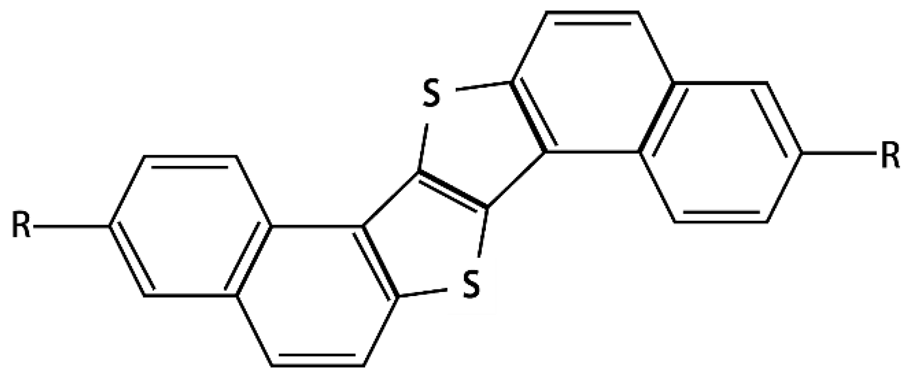
Figure 2.
a) The DFT simulation of non-resonance Raman spectrum of S-DNTT-10 in the range of 1100-1550 cm-1, the overall spectrum in Figure S2, (b) the measured non-resonance Raman spectrums of 700 nm S-DNTT-10 thin-film in 1100 - 1550 cm-1 range. (The excitation wavelength = 532 nm, illumination laser power = 6.22 mW, objective lens 50×, N.A. = 0.5; exposure time = 30 s, accumulation times = 3, the used grating of 1800 grooves/mm) (c) the vibrational mode 1, and (d) the vibrational mode7.
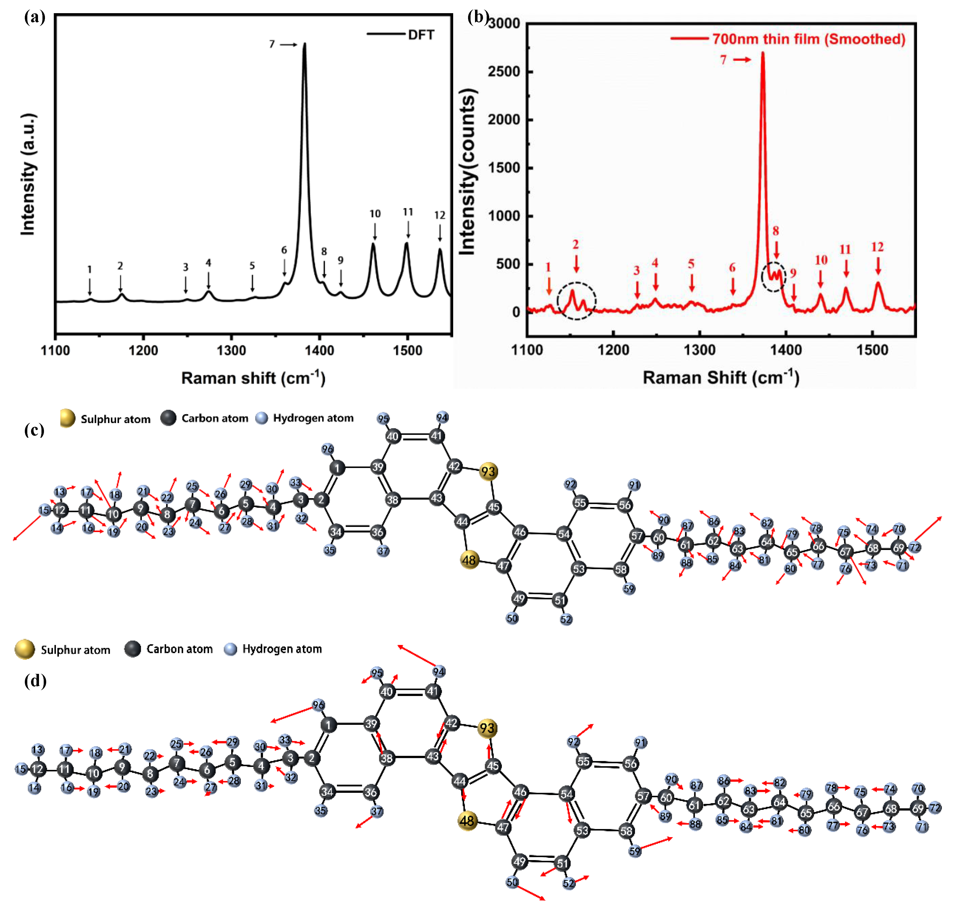
Figure 3.
The non-resonant Raman spectrum of the S-DNTT-10 thin film with different thickness using 532 nm laser.
Figure 3.
The non-resonant Raman spectrum of the S-DNTT-10 thin film with different thickness using 532 nm laser.
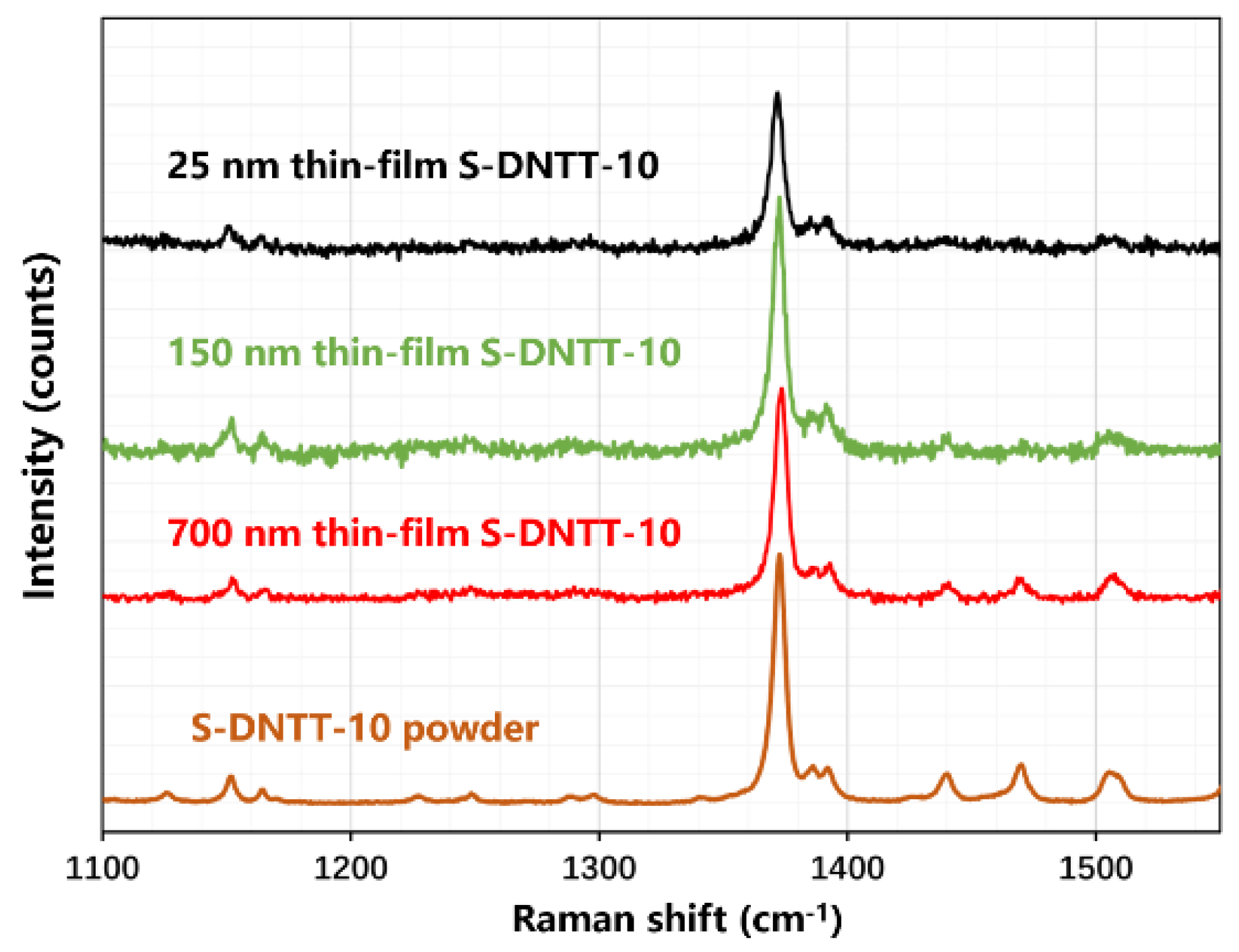
Figure 4.
The SERS spectrums for S-DNTT-10 molecules depositing by different thickness of Au thin-films under lasers of (a) 532nm, output power = 3.11 mW, exposure time = 20 s, accumulation times = 2, grating = 300 grooves/mm, (b) 633 nm, output power = 0.605 mW, exposure time = 17 s, accumulation times = 2, grating = 300 grooves/mm and (c) 785 nm with baseline-treatment, output power = 2.1 mW, exposure time = 14 s, accumulation times = 2, grating = 300 grooves/mm.
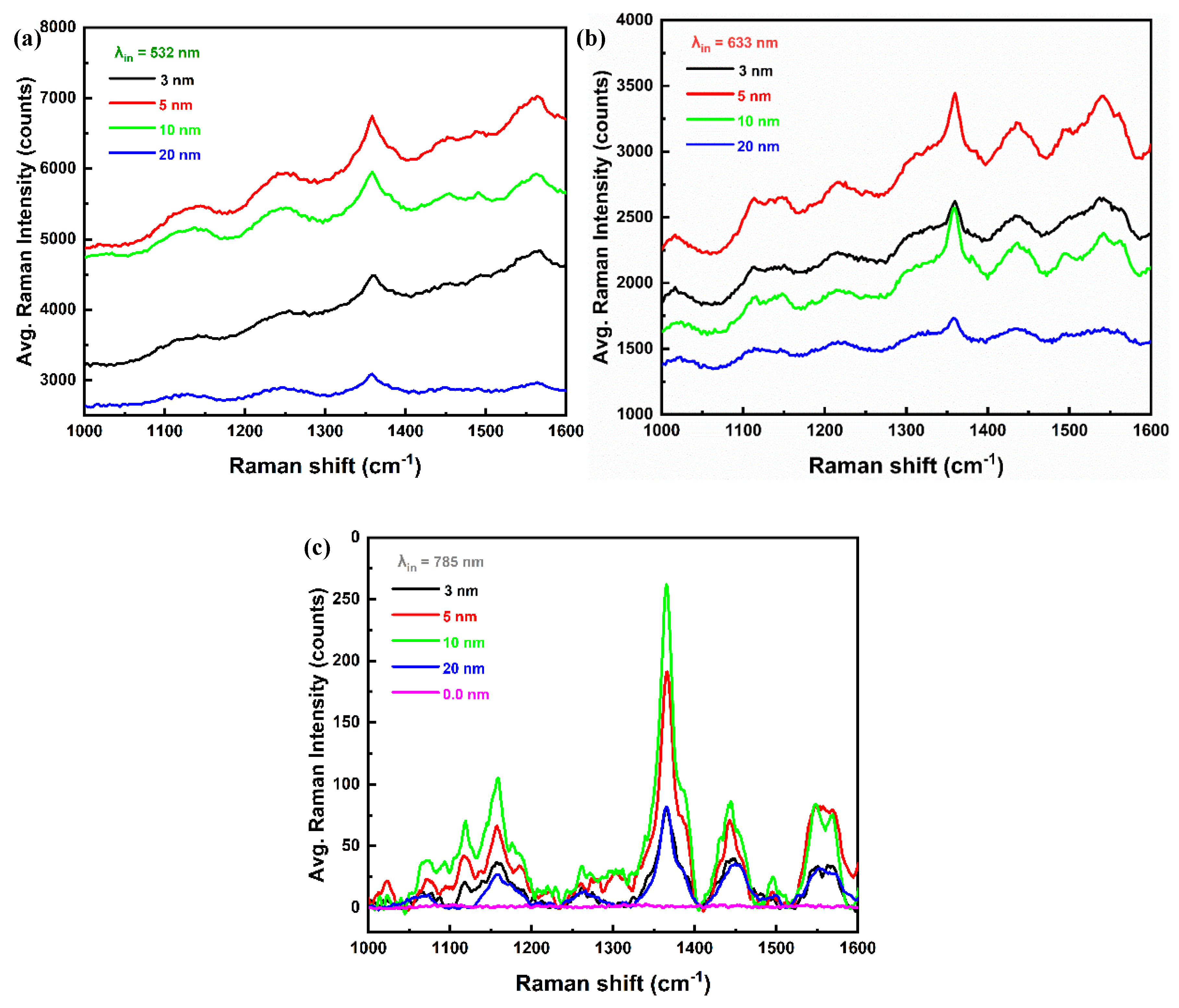
Figure 5.
a) The schematic representation of fundamental surface Plasmon (SP) mechanism of SERS. The AFM topography with top-view optical-image in different thickness of Au thin-films: (b) 3 nm, (c) 5 nm, (d) 10 nm and (e) 20 nm. (f) The diagram of Fermi level of gold and molecular orbitals of S-DNTT-10 molecule.
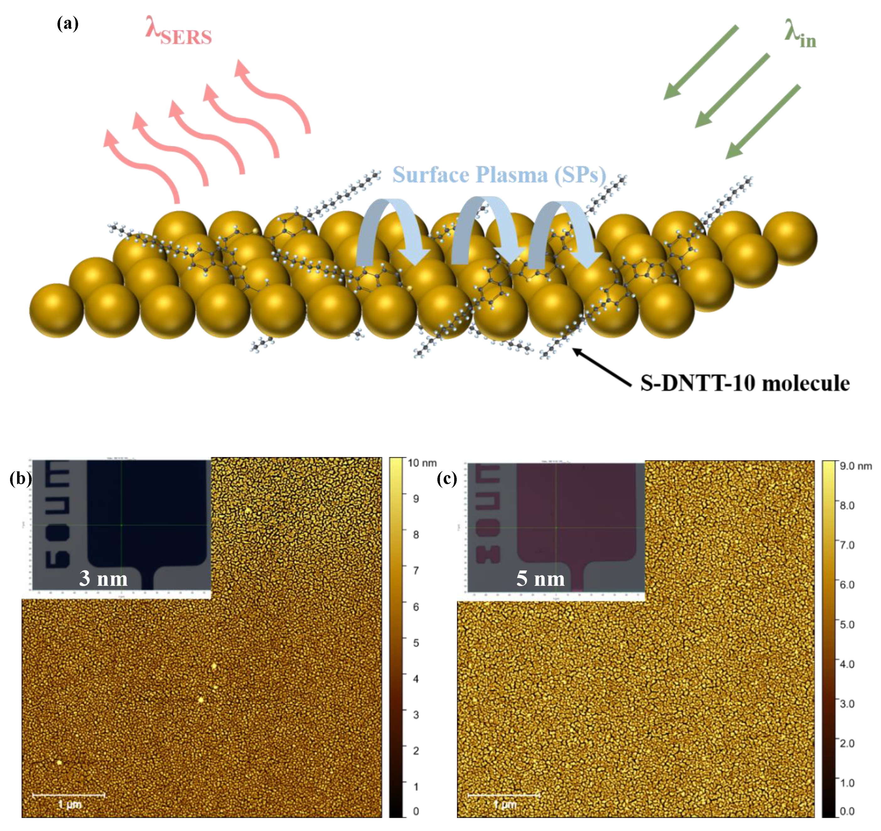
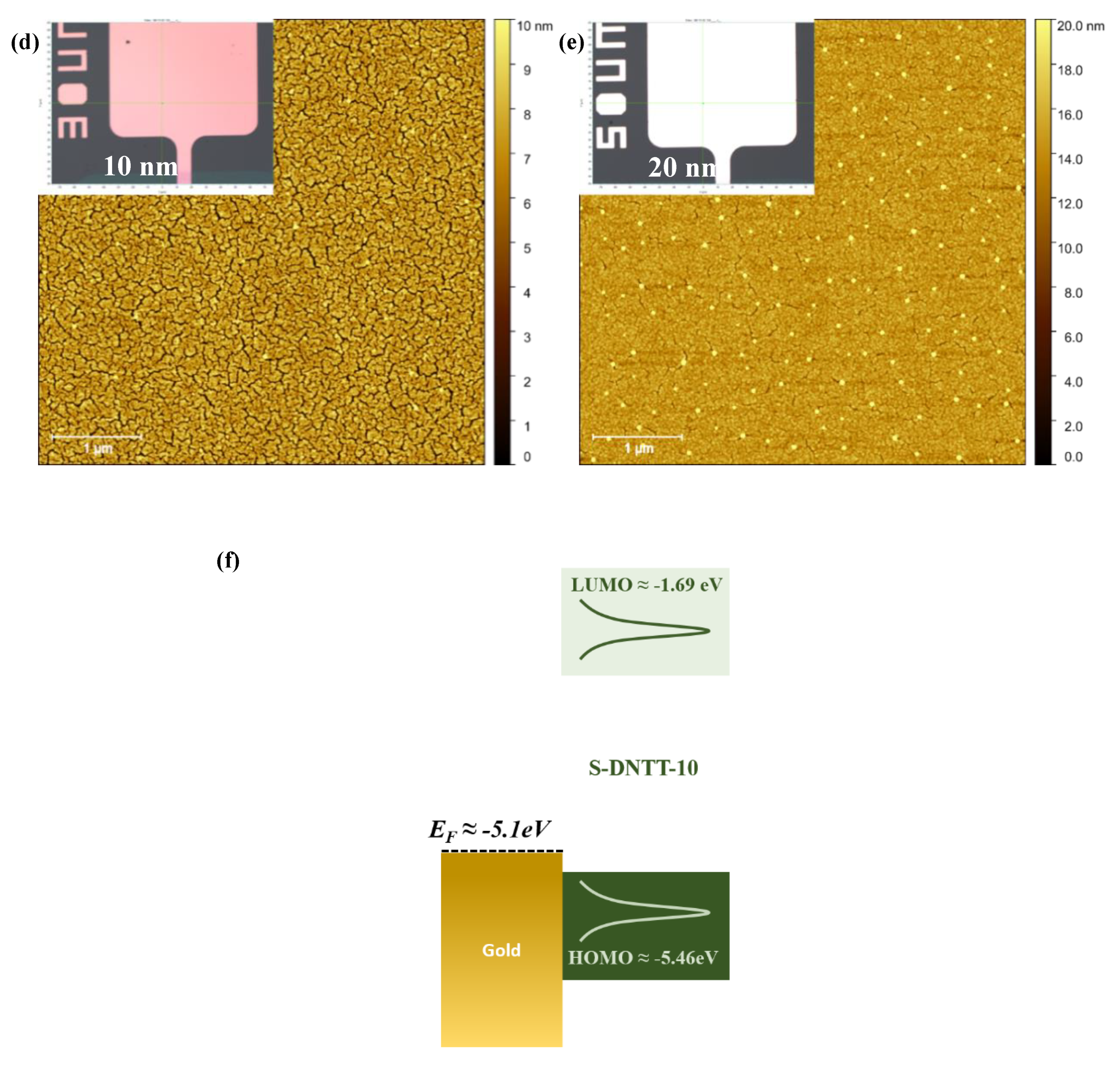
Figure 6.
a) The comparison of S-DNTT-10-SERS spectrum under 785 nm and S-DNTT-10-conventional Raman spectrum under 532 nm. (b) The comparison of simulated Raman spectrum of one single S-DNTT-10 molecule and hybridized S-DNTT-10 molecule. (c) The hypothetical S-DNTT-10 hybridized with marked hydrogen molecule.
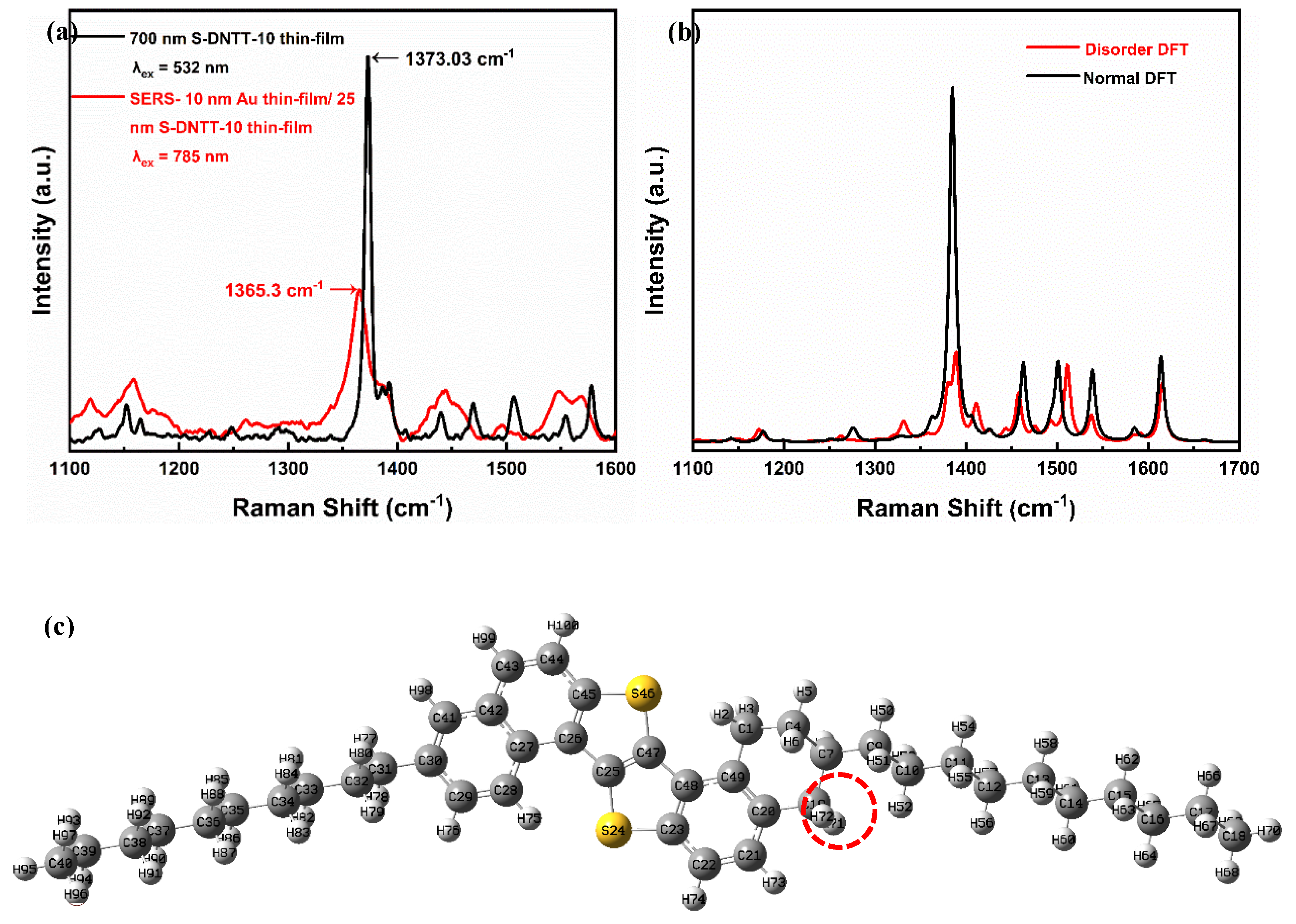
Figure 7.
The schematic representation of Au atom potentially diffusing into S-DNTT-10 molecules.
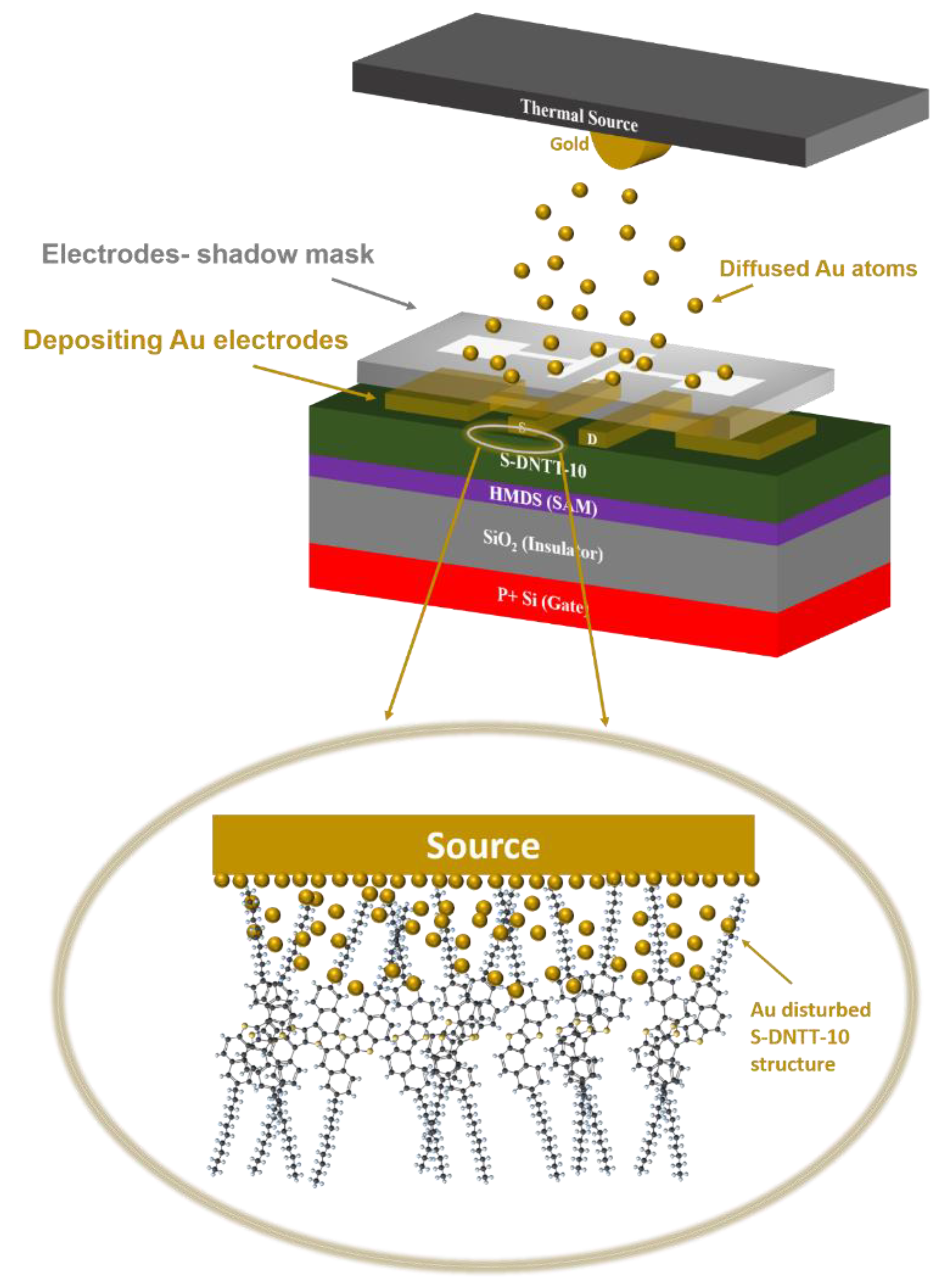

Table 1.
The details of DFT simulated vibrational modes.
| Mode | Raman shift/cm-1 | Vibrational modes descriptions |
|---|---|---|
| 1 | 1141.79 | C-H bond bending at alkyl chains |
| 2 | 1177.11 | C-H bond bending located at the aromatic rings and coupled with few slight deformations of thiophene rings |
| 3 | 1251.53 | C-H bond bending at alkyl chains; C-H bond bending coupled with slight breathing stretching aromatic rings and thiophene rings deformed |
| 4 | 1274.84 | C-H bond bending at alkyl chains; some serious C-H bond bending located at C(38), C(33), C(93), C(86), C(81) and C(45), and coupled with few slight deformation of aromatic and thiophene rings |
| 5 | 1328.95 | C-H bond anti-symmetry bending at alkyl chains coupled with C-C bond movement at aromatic and thiophene rings |
| 6 | 1362.20 | C-H bond bending at alkyl chains; deformation of thiophene rings and linked aromatic rings; seriously C-H bond bending located at C(36), C(95), C(84) and C(47); C-C bond stretched at aromatic and thiophene rings |
| 7 | 1384.79 | C-H bond slightly bending at alkyl chains; strongly C-H bond bending located at C(38), C(33), C(86) and C(81) coupled with deformation of aromatic and thiophene |
| 8 | 1406.24 | C-H bond slightly bending at alkyl chains; strongly C-H bond bending located at C(36), C(93), C(84) and C(85) and C(42)=C(90) double-bond stretching coupled with deformation of aromatic and thiophene |
| 9 | 1426.09 | slight C-H bond bending at the end of alkyl chains; strong C-H bond bending at C(36), C(33), C(95), C(86), C(81) and C(47) coupled with deformation of aromatic and thiophene rings. |
| 10 | 1462.96 | C(42)-C(43) and C(90)-C(91) strongly stretching coupled with deformation of aromatic and thiophene rings |
| 11 | 1500.85 | C-H slightly bending at the end of alkyl chains; deformation of aromatic and thiophene rings |
| 12 | 1539.00 | strongly C(42) = C(90) double-bond stretching coupled with deformation of aromatic and thiophene rings |
Disclaimer/Publisher’s Note: The statements, opinions and data contained in all publications are solely those of the individual author(s) and contributor(s) and not of MDPI and/or the editor(s). MDPI and/or the editor(s) disclaim responsibility for any injury to people or property resulting from any ideas, methods, instructions or products referred to in the content. |
© 2025 by the authors. Licensee MDPI, Basel, Switzerland. This article is an open access article distributed under the terms and conditions of the Creative Commons Attribution (CC BY) license (http://creativecommons.org/licenses/by/4.0/).
Copyright: This open access article is published under a Creative Commons CC BY 4.0 license, which permit the free download, distribution, and reuse, provided that the author and preprint are cited in any reuse.


