
Submitted:
27 September 2023
Posted:
28 September 2023
You are already at the latest version
Abstract
Metallic masters can be used as a metallic mold to replicate polymeric pieces with high resolution. Metallic masters with high resolution were created by photolithography technique and nickel electrodeposition technique. AZ 9260 photoresists and SPR 220-7.0 photoresists were used to coat metallic substrates and to compare results. Steel substrate and nickel substrate were used as the metallic substrate to compare results. Two different nickel electrodeposition protocols were used to compare results. In the conclusion section, was determined the best photoresist, metallic substrate, and nickel electrodeposition protocol to fabricate metallic masters.
Keywords:
electrodeposition
; master
; microfabrication
; nickel
; photoresist
INTRODUCTION
E2dish [1] and PDMS cap [2] are biomedical devices that use electrophysiology to record neural electrical activity of the neurons. It is necessary a mold to build the polymeric devices.
Injection molding, hot embossing, and elastomer casting are some of the popular manufacturing processes used to replicate polymeric pieces with high resolution [3]. All these manufacturing processes start with a masterpiece. The masterpiece is a mold with a negative image of the final form that it is looking for. Masterpiece creation is an essential and crucial part of the replication process. Any imperfection from the masterpiece would be replicated over all the polymeric pieces.
Masterpiece usually is a glass disk with a SU-8 photoresin strip. The polymeric material is casted over the masterpiece to obtain a polymeric piece with a positive image. After several casting repetitions, the SU-8 photresin strip deteriorates.
Injection molding and hot embossing techniques require a metallic master to replicate polymeric pieces with high resolution (structures at micrometer scales). Elastomer casting technique can work with both masterpieces, the metallic or the glass disk.
This paper focuses on the microfabrication of metallic masters with metallic lines by nickel electrodeposition technique. The nickel electrodeposition technique is the most suitable manufacturing technique to obtain a metallic master [4,5].
The electrolytic solution is the key to the nickel electrodeposition technique. The electrolyte composition of the nickel electrodeposition solution is also known as Nickel Sulfamate Solution [6]. The elements and concentrations of an electrolytic solution varied according to the needs of the research group. For example, Pai et al., and Kukharenka & Kraft used electrodeposition over a master with photoresist SPR to get a resolution of 3.6 μm [7,8] meanwhile, Lee, Hirai, and Ueno used electrodeposition over various photoresists to get less than 10 µm [9,10,11].
However, certain compounds within the electrolytic solution can improve the electrodeposition quality [12,13]. Liebelight SF-1 and Liebelight SF-2 function as wetting agents for surface irregularities on the finish of the electrodeposited material [14]. Saccharin reduces stress levels at the master [15]. Sodium dodecyl sulfate (SDS) improves the high-resolution detail, avoids stress level, and avoids deformation at the electrodeposited material [6].
The goal of this investigation is to improve the fabrication process of metallic master to be used as a mold (negative image) to replicate a high number of polymeric pieces (positive image). The metallic master should be a metallic disk with flat surface, and a metallic line of 5 μm high, 20 μm wide, and 1 mm long. The microchannel should allow to the neurites of the neuron to grow across it interior.
MATERIALS AND METHODS
Three combinations of photoresist and metallic substrate were evaluated to create metallic masters: 1) AZ 9260 photoresist over steel substrate, 2) SPR 220-7.0 photoresist over steel substrate, and 3) SPR 220-7.0 photoresist over nickel substrate.
The microfabrication process to create a metallic master consisted of two steps. The first step of master microfabrication consisted of coating a thin film of photoresist over a metallic substrate. Two optional protocols were evaluated to determine the best photoresist option to be applied. The optional protocols were denominated as “Protocol with AZ 9260 photoresist” and “Protocol with SPR 220-7.0 photoresist”. After “Protocol with AZ 9260 photoresist” or “Protocol with SPR 220-7.0 photoresist” was applied, the metallic substrate was put through to spinning, heating, and photolithography techniques. The photolithography technique created trenches of 10 mm long, 20 µm wide, and 5 µm thick.
The second step of master microfabrication consisted to create thin metallic lines adhered to the metallic substrate. Two kinds of metallic substrates (steel and nickel) were evaluated to determine the best quality. Both, steel substrate and nickel substrate had the surface quality of mirror polished with waviness height less than 0.1 μm and roughness less than 0.002 μm.
The second step of master microfabrication used the nickel electrodeposition technique to deposit nickel ions in the photoresist trench from the metallic substrate. Once the nickel electrodeposition process was finished, the photoresist was removed by a chemical process. The final form of the metallic master was a metallic substrate (flat surface) with metallic lines (10 mm long, 20 µm wide, and 5 µm high).
First step of master microfabrication (photoresist deposition)
Protocol with AZ 9260 photoresist
AZ 9260 is a positive photoresist designed for film thickness from 2 µm to 24 µm resolution [16].
Photolithography with AZ 9260 photoresist consisted: AZ 9260 Photoresist was deposited on a metallic substrate. The metallic substrate was collocated over a spinner. The spinner was run with the parameters of Table 1, to get 5 μm thickness of photoresist. Then, the metallic substrate was removed from the spinner and deposited on the hot plate for 2.5 min at 95 °C to remove humidity.
The metallic substrate was placed in the photolithography machine. A mask with a pattern of straight lines was collocated over the metallic substrate. The photolithography machine operated for one cycle only, configurated for soft-contact, and an exposure time of 20 seconds. After the photolithography exposition, the metallic substrate was ringed with AZ 726MIF developer for 3 to 4 minutes, to remove the photoresist exposed parts.
Protocol with SPR 220-7.0 photoresist
SPR 220-7.0 is a positive photoresist for general uses and designed for film thickness from 1 to 30 µm. The SPR photoresist has excellent adhesion and coating characteristics, which makes it very useful for MEMS and electrodeposition applications [7].
Photolithography with SPR 220-7.0 photoresist consisted: The metallic substrate was pre-heated for 30 minutes at 180 °C. Hexamethyldisilazane (HMDS) was coated over the metallic substrate as an adhesion promoter between the photoresist and the metallic substrate. The metallic substrate was placed on the spinner. The spinner was run with the parameters of Table 2 to remove the HMDS excess. SPR 220-7.0 photoresist was deposited on the metallic substrate. The spinner was run with the parameters of Table 2 again to get 5 μm thickness of photoresist. The metallic substrate was collocated in an oven to be heated for 15 min at 150 °C to remove humidity.
The metallic substrate was placed in the photolithography machine. A mask with a pattern of straight lines was collocated over the metallic substrate into the photolithography machine. The photolithography machine operated for only one cycle, configurated for soft-contact, and an exposure time of 90 seconds. The metallic substrate was collocated inside a petri dish to rest for 45 minutes. Then, this substrate was immersed in two different containers with an MF-24A developer for one minute each to remove the parts of the photoresist exposed.
Second step of master microfabrication (nickel electrodeposition)
The nickel electrodeposition technique was used to create metallic lines over the metallic substrate. The nickel electrodeposition technique consisted of two electrodes (nickel plate and metallic substrate coated with photoresist) introduced in a nickel-rich electrolytic solution to create a closed circuit. Electrical current was applied on the closed-circuit; the anode ions (nickel plate) were deposited on the exposed area of the cathode's conductive surface (photoresist trenches) to create nickel lines at the metallic substrate.
Protocol A.
Steel substrate was put through a pre-activation stage after the first step of master microfabrication. The pre-activation stage consisted of the steel substrate being immersed in a chemical solution at room temperature for one minute. The chemical solution consisted of 50% hydrochloric acid (HCl) and 50% distilled water (H2O).
Steel substrate was put through an activation stage after the pre-activation stage. The activation stage consisted that the steel substrate was immersed in a different chemical solution called Woods bath. The chemical composition of the Woods bath was 25% Nickel Chloride (), 25% Hydrochloric Acid (HCl), and 50% Distilled Water (). The activation stage was at room temperature and with a circulating current of 50 for 3 minutes. The purpose of the Woods bath was to guarantee high-quality and stronger adherence of the nickel line to the steel substrate.
Steel substrate was immersed into another different electrolytic solution called Watts bath (or nickel sulfamate). Table 3 shows the chemical composition of the Watts bath to prepare 500 ml of an aqueous solution for the electrodeposition process with nickel. The Watts bath was at 55 °C and pH near to 4 units.
The literature recommended that the current density for a high deposition rate has to be below 20 7,10,15. A current of 10 was applied, at a temperature of 55 °C, for 3 hours. A current of 10 was equivalent to deposit 2 μm nickel layer every hour. Nickel ions were deposited at the trenches of the photoresist film over the steel substrate.
Protocol B
Nickel substrate was put through an activation stage after the first step of master microfabrication. In the activation stage, the nickel substrate was immersed in a chemical solution called Woods bath. The chemical composition of Woods bath was 25% Nickel Chloride (), 25% Hydrochloric Acid (HCl), and 50% Distilled Water (). The activation stage was at room temperature and a circulating current of 12 500 for 2 minutes. The purpose of the Woods bath was to guarantee high-quality and stronger adherence of the nickel line to the nickel substrate.
Nickel substrate was immersed into a Watts bath solution. Table 3 shows the chemical composition of the Watts bath to prepare 500 ml of an aqueous solution for the electrodeposition process with nickel. The Watts bath solution was at 55 °C and pH of 2.92. A current of 12 500 was applied. To evaluated the appropriate immersion time, some nickel substrates were immersed for 8 minutes, other nickel substrates were immersed for 15 minutes.
RESULTS AND DISCUSSION
The result of the first step of master microfabrication was a metallic substrate (steel or nickel) coated with a photoresist film (AZ 9260 or SPR 220-7.0). The photoresist film formed trenches. The trenches were lineal areas without photoresist where the metallic substrate was exposed.
The results showed the morphology of the trenches formed by different combinations of metallic substrates and photoresists.
1.- Steel and nickel substrate coated with AZ 9260 photoresist formed trenches with irregularities. Figure 1 shows the irregularities of a trench.
2.- Steel and nickel substrate coated with SPR 220-7.0 photoresist formed trenches with a standard deviation of 0.58 µm at the edges. Figure 2 shows the morphology of a trench.
3.- Nickel substrate coated with SPR 220-7.0 photoresist formed trenches with a similar appearance in Fig. 2.
The results of the second step of master microfabrication were a metallic substrate with nickel lines without photoresist.
Results of AZ 9260 photoresist and SPR 220-7.0 photoresist
AZ 9260 photoresist slightly comes off when the metallic substrate was immersed in the nickel sulfamate solution. SPR 220-7.0 photoresist also slightly comes off from the metallic substrate when it was immersed in the nickel sulfamate solution. The evaluation showed that SPR 220-7.0 photoresist detached in a lower proportion than AZ 9260 photoresist.
Results of Protocol A and Protocol B.
In Protocol A, Nickel lines electrodeposited to steel substrate can be easily detached by scratching with a plastic tip. And Protocol B had the same results from nickel substrates immersed for 8 minutes as nickel substrates immersed for 15 minutes.
Nickel lines electrodeposited with Protocol B were more difficult to detach than nickel lines electrodeposited with Protocol A. Nickel lines electrodeposited with Protocol B had low morphological quality as shown in Figure 3. Figure 3 also shows a complete nickel line over the metallic substrate, but it also shows the amplification of the nickel line and its irregularities.
Figure 4 shows scanning electron microscope images of a nickel substrate with nickel lines. Figure 4 (A) shows a 60° incline view of a nickel substrate with some irregularities from the nickel line. Figure 4 (B) shows that some part of the nickel was electrodeposited outside the line area because there was some filtration of the chemical solution under the photoresist film. Figure 4 (C) shows the top view of the nickel substrate with boulders at the edges of the nickel line.
The nickel line in Fig. 4 (C) was measured by Veeco Profilometer measured. The nickel line had a maximum width of 40 µm and a minimum width of 30 µm (Fig. 5). Figure 5 shows two peaks at the nickel line. The two peaks represented a high concentration of nickel ions.
The main goal of this work was to create a metallic substrate with metallic lines; a metallic master. A metallic master can be used as a mold in the injection molding technique to fabricate several polymeric pieces. The metallic substrate must have strong and homogeneous metallic lines to guarantee great quality in the replication process of polymeric pieces. The metallic master must be perfect.
At the beginning of the fabrication process, the metallic substrate was coated by a photoresist film. Some trenches were created at the photoresist film over the metallic substrate. The trenches were the lineal areas where the nickel ions will be adhered by electrodeposition technique.
Some imperfections were detected on the metallic master as a consequence of the poor adherence of the photoresist to the metallic substrate. For example, when the metallics substrates were immersed into the nickel sulfamate solution, the SPR 220-7.0 photoresist and AZ 9260 photoresist detached from the metallic substrate and it compromised the areas of the lines where the nickel lines were electrodeposited.
Results indicated that SPR 220-7.0 photoresist had better adhesion to the metallic substrate and chemical resistance, but also better trenches (Fig. 2) than AZ 9260 photoresist. Because AZ 9260 photoresist created irregular trenches (Fig. 1) irregular nickel lines were created. Therefore, irregular nickel lines from a metallic substrate equal an irregular metallic master. And an irregular metallic master reproduces low-quality polymeric pieces by any techniques like hot embossing or injection molding. So, AZ 9260 photoresist should not be recommended to use for microfabrication.
Protocol A created nickel lines with homogenous morphology, but poor adhesion to the metallic substrate. Protocol B created nickel lines with heterogenous morphology, but strong adhesion to the metallic substrate. Therefore, the recommendation for future work is to use Protocol B steps with the current density of Protocol A (from 10 ) during the Watts bath solution. The change of the current density should improve the nickel lines to be homogenous morphology and strong adherence to the metallic substrate.
The high concentration of nickel ions in the electrodeposition process created some boulders at the edges of the nickel line as shown in Fig. 4 (C). Figure 5 shows that the profilometer measured the nickel boulders at the top of some nickel lines. These nickel boulders should be a consequence of applying high current density (12 500 ) during the nickel electrodeposition process.
A suggestion, as an alternative to all the processes of AZ 9260 or SPR220-7.0 photoresist, and electrodeposition technique is to fabricate lines with SU-8 photoresist by the photolithography technique. SU-8 photoresists can fabricate lines with homogenous morphology and strong adherence to the metallic substrate. But, the masters with lines fabricated by SU-8 photoresist will not be very effective as a mold to replicate a high number of polymeric pieces.
CONCLUSIONS
At the first step of master microfabrication, SPR 220-7.0 photoresist had better adhesion to the metallic substrate than AZ 9260 photoresist because SPR 220-7.0 photoresist created better nickel lines than AZ 9260 photoresist.
At the second step of master microfabrication, Protocol A created nickel lines with better morphology than Protocol B. However, Protocol B created nickel lines with stronger adhesion than Protocol A; nickel lines adhered better to a nickel substrate than a steel substrate.
In conclusion, this research establishes the best protocol to microfabricate a metallic master as mold to cast polymeric pieces to confine neurons and to record neural electrical activity as contribution to biomedical engineering. The best protocol consists of: 1) A nickel substrate coated with SPR 220-7.0 by photolithography process. 2) The nickel substrate is immersed into an activation stage of 25% Nickel Chloride (), 25% Hydrochloric Acid (HCl), and 50% Distilled Water () at room temperature and a density current of 12 500 for 2 minutes. 3) Then, the nickel substrate is immersed into a Watts bath solution (Table 3 shows the chemical composition) at 55 °C, pH of 2.92 and a density current of 10 for 8 minutes.
Ethical statement
Any live subjects be required.
Acknowledgments
Special thanks for their participation in the translation of this article: Espinosa-Alvizo, C., I.; Sierra-Cuellar, G.; Anda-Moncada, M., L.; Zamora-Leyva A., R.
Conflicts of Interest
The author does not report any conflict of interest.
References
- Morales, R.; Riss, M.; Wang, L.; Gavín, R.; Del Río, J.A.; Alcubilla, R.; Claverol-Tinturé, E. Integrating multi-unit electrophysiology and plastic culture dishes for network neuroscience. Lab a Chip 2008, 8, 1896–1905. [Google Scholar] [CrossRef]
- Habibey, R.; Latifi, S.; Mousavi, H.; Pesce, M.; Arab-Tehrany, E.; Blau, A. A multielectrode array microchannel platform reveals both transient and slow changes in axonal conduction velocity. Sci. Rep. 2017, 7, 1–14. [Google Scholar] [CrossRef] [PubMed]
- Becker, H.; Gärtner, C. Polymer microfabrication technologies for microfluidic systems. Anal. Bioanal. Chem. 2007, 390, 89–111. [Google Scholar] [CrossRef] [PubMed]
- Mekaru, H.; Yamada, T.; Yan, S.; Hattori, T. Microfabrication by hot embossing and injection molding at LASTI. Microsyst. Technol. 2004, 10, 682–688. [Google Scholar] [CrossRef]
- Piotter, V.; Hanemann, T.; Ruprecht, R.; Haußelt, J. Injection molding and related techniques for fabrication of microstructures. Microsyst. Technol. 1997, 3, 129–133. [Google Scholar] [CrossRef]
- Kelly JJ, Yang NYC. ELECTRODEPOSITION OF NI FROM A Part I. Effect of a Stress Relief on Annealing Behavior and Film Metallurgy. 2001. TOPICAL (SAND--2001-8609). United States.
- Kukharenka, E.; Kraft, M. Realization of electroplating molds with thick positive SPR 220-7 photoresist. J. Mater. Sci. Mater. Electron. 2003, 14, 319–322. [Google Scholar] [CrossRef]
- Pai, RS. Nickel Electroplating using Shipley Megaposit SPR 220 Positive Resist as a Mold. Time [Internet]. 2001. p. 1–7. Available from: https://nanopdf.com/download/nickel-electroplating_pdf#.
- Hirai, Y.; Harada, S.; Isaka, S.; Kobayashi, M.; Tanaka, Y. Nano-imprint lithography using replicated mold by Ni electroforming. Japanese J Appl Physics, Part 1 Regul Pap Short Notes Rev Pap 2002, 41, 4186–4189. [Google Scholar] [CrossRef]
- Lee, C.H.; Jiang, K. Fabrication of thick electroforming micro mould using a KMPR negative tone photoresist. J. Micromechanics Microengineering 2008, 18. [Google Scholar] [CrossRef]
- Ueno, H.; Hosaka, M.; Zhang, Y.; Tabata, O.; Konishi, S.; Sugiyama, S. Study on fabrication of high aspect ratio microparts using the LIGA process. MHS 1997 - Proc 1997 Int Symp Micromechatronics Hum Sci. 1997, 49–54. [CrossRef]
- Monzón Verona M, Hernández Castellano P, Marrero Alemán, Ma D, Benítez Vega A. 8° Congreso Iberoamericano de Ingeniería Mecánica. In: Applications of electroforming for rapid tool manufacturing [Internet]. 2007. Available from: https://congreso.pucp.edu.pe/cibim8/pdf/25/25-07.pdf.
- Zhu, X.; Liu, G.; Xiong, Y.; Guo, Y.; Tian, Y. Fabrication of PMMA Microchip of Capillary Electrophoresis by Optimized UV-LIGA Process. J Phys Conf Ser 2006, 34, 875–879. [Google Scholar] [CrossRef]
- Lim, J.H.; Park, E.C.; Lee, S.Y.; Yoon, J.-W.; Ha, S.-S.; Joo, J.; Lee, H.-J.; Jung, S.-B.; Song, K. Fabrication of Ni Metal Mask by Electroforming Process Using Wetting Agents. J. Electron. Mater. 2007, 36, 1510–1515. [Google Scholar] [CrossRef]
- Subramanian, A.; Srinivasan, K.; John, S.; Vasudevan, T. Recovery of activated nickel from residues for electroforming applications. J. Appl. Electrochem. 2001, 31, 35–40. [Google Scholar] [CrossRef]
- Chen, S.C.; Cheng, C.H.; Lin, Y.C. Fabrication of components for a valve-less micropump or microejector by multilevel electroforming technology. Microsyst. Technol. 2007, 13, 455–463. [Google Scholar] [CrossRef]
Figure 1.
Trench with AZ photoresist on a steel substrate.
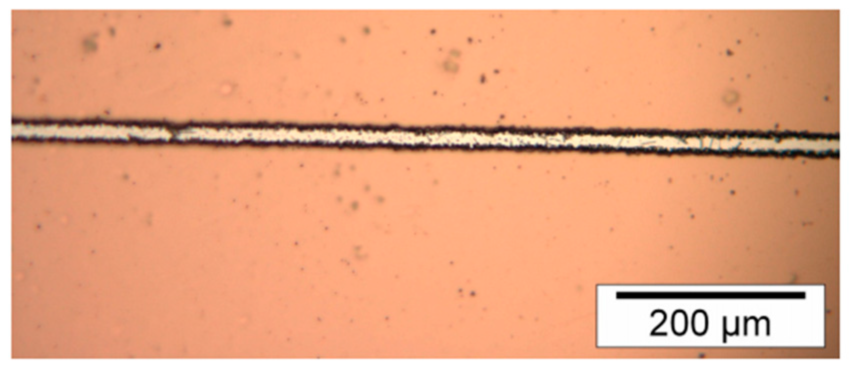
Figure 2.
Trench of the SPR photoresist on a steel substrate.
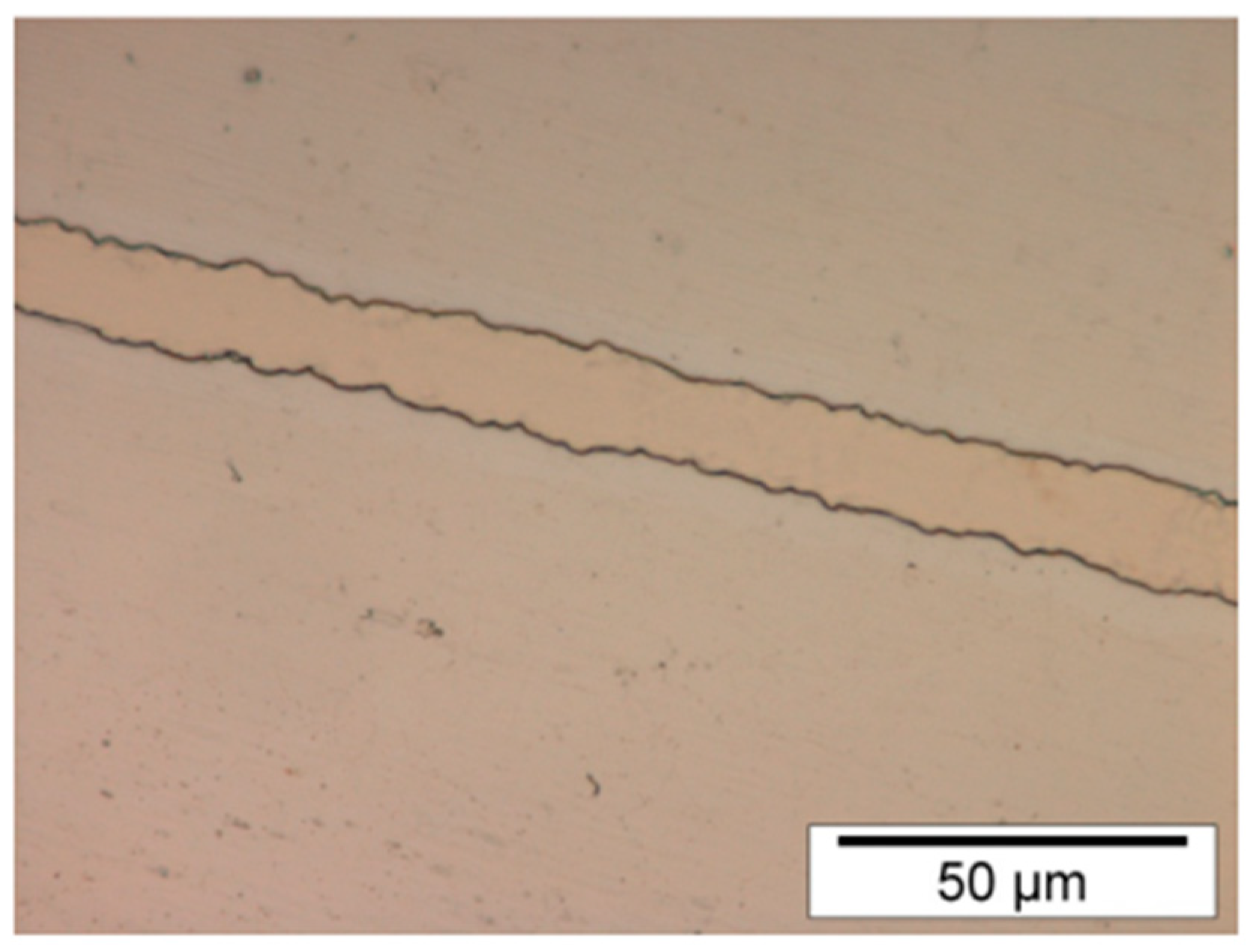
Figure 3.
Electrodeposited nickel line on a nickel substrate.
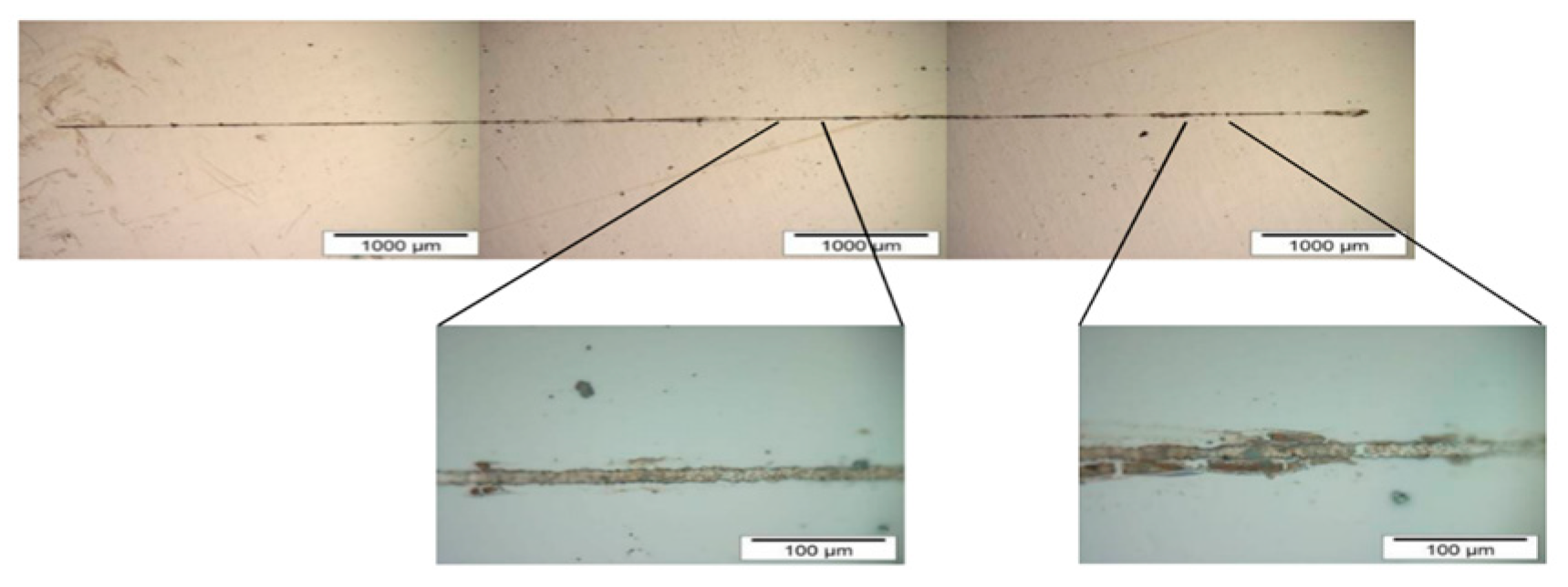
Figure 4.
Scanning electron microscope images of the electrodeposition of a nickel line on nickel master.
Figure 4.
Scanning electron microscope images of the electrodeposition of a nickel line on nickel master.
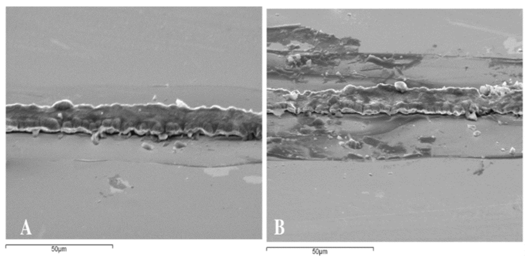
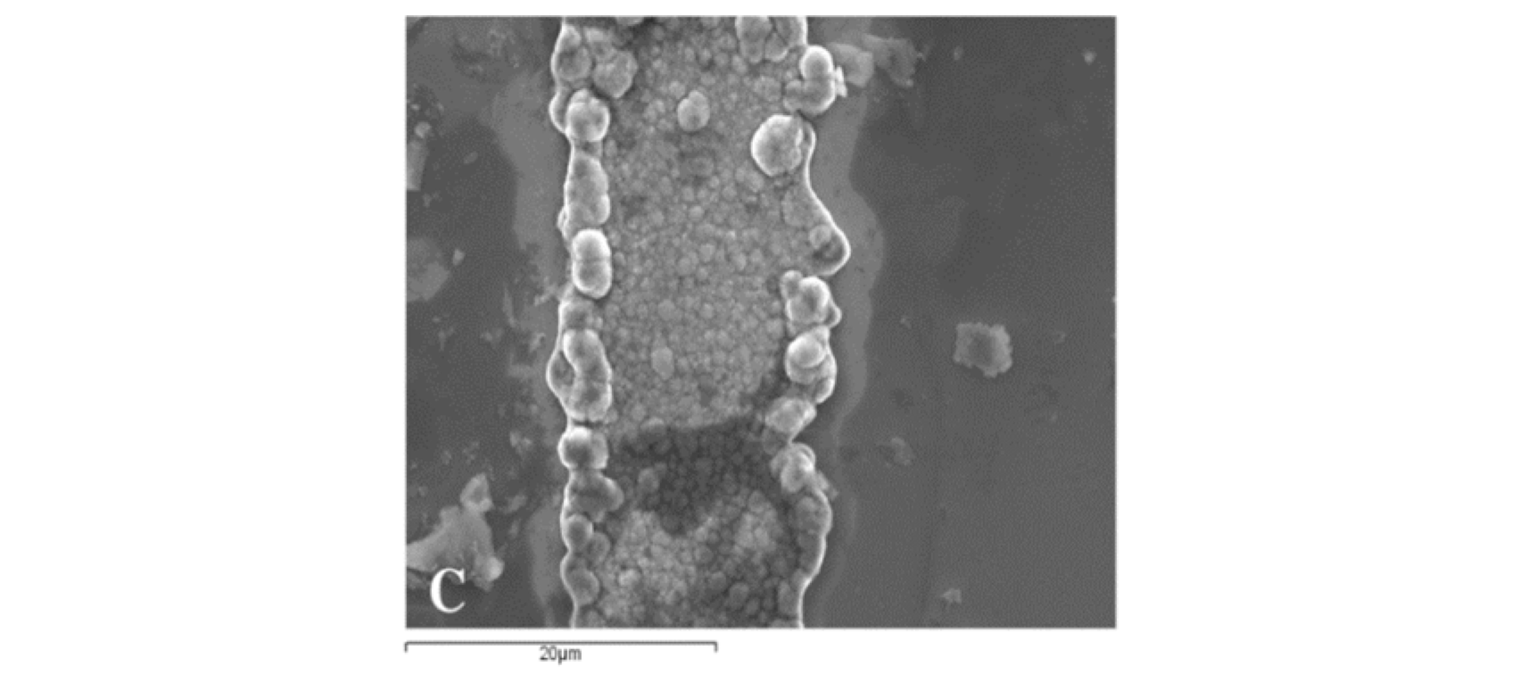
Figure 5.
Measurement of the cross-section of the nickel line with a profilometer.
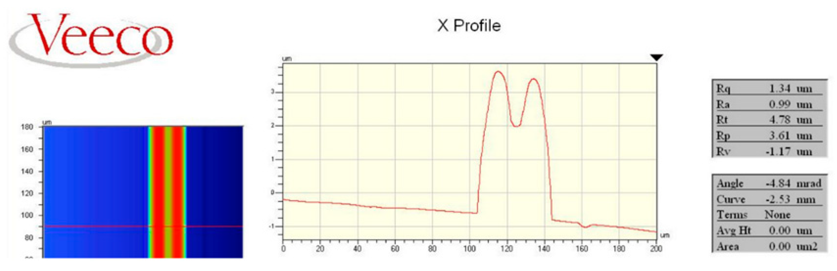

Table 1.
Spinner configuration for AZ 9260 photoresist.
| Time | Speed |
|---|---|
| 10 s | 500 RPM |
| 40 s | 4000 RPM |
Table 2.
Spinner configuration for SPR 220-7.0 photoresist.
| Time | Speed |
|---|---|
| 10 s | 500 RPM |
| 40 s | 3000 RPM |
Table 3.
500 ml of Watts bath (Nickel Sulfamate Solution).
| Compound | Formula | Quantity |
|---|---|---|
| Nickel sulfamate | 298.5 gr | |
| Boric acid | 22.5 gr | |
| Saccharin | 1.0 gr | |
| Sodium dodecyl sulfate (SDS) | 0.1 gr | |
| Distilled water | 500.0 ml |
Disclaimer/Publisher’s Note: The statements, opinions and data contained in all publications are solely those of the individual author(s) and contributor(s) and not of MDPI and/or the editor(s). MDPI and/or the editor(s) disclaim responsibility for any injury to people or property resulting from any ideas, methods, instructions or products referred to in the content. |
© 2023 by the authors. Licensee MDPI, Basel, Switzerland. This article is an open access article distributed under the terms and conditions of the Creative Commons Attribution (CC BY) license (http://creativecommons.org/licenses/by/4.0/).
Copyright: This open access article is published under a Creative Commons CC BY 4.0 license, which permit the free download, distribution, and reuse, provided that the author and preprint are cited in any reuse.


