
Submitted:
20 January 2026
Posted:
22 January 2026
You are already at the latest version
Abstract
This paper presents the design and validation of an enhanced clock architecture for White Rabbit Switches, addressing the growing need for ultra-precise synchronization in distributed systems. The White Rabbit protocol enables sub-nanosecond timing alignment and deterministic data transmission over optical fiber networks, making it a cornerstone for applications in high-energy physics, telecommunications, and industrial automation. Achieving this level of precision depends critically on the stability and integrity of the clock distribution system. To meet these requirements, the proposed architecture introduces a redundant oscillator subsystem that integrates two independent clock paths: one based on high-stability crystal oscillators and another on voltage-controlled oscillators. This dual-path design provides automatic failover capability, ensuring continuous operation under fault conditions. By directly generating the 125 MHz and 124.992 MHz signals required by the White Rabbit protocol, the system eliminates intermediate frequency synthesis stages, significantly reducing phase noise and jitter. The design process incorporates advanced signal and power integrity simulations to optimize Printed Circuit Board layout, impedance control, and power distribution network performance. These simulations confirm that the proposed architecture achieves low-jitter operation while maintaining compatibility with existing White Rabbit infrastructure. Detailed jitter analysis demonstrates substantial improvements in synchronization reliability, paving the way for robust deployment in large-scale scientific and industrial networks.
Keywords:
Subnanosecond synchronization
; White Rabbit
; IEEE Std 1588-2019
; virtual prototyping
1. Introduction
Modern technological systems increasingly demand ultra-precise synchronization to guarantee optimal performance across diverse domains. In telecommunications, for instance, phase alignment among Radio Access Network (RAN) nodes is essential for 5G New Radio and emerging wireless technologies to maintain low latency and high reliability [1,2,3]. Recent studies confirm that tighter synchronization directly enhances spectral efficiency in massive Multiple-Input Multiple-Output (MIMO) deployments [4]. Similarly, large-scale data centers depend on accurate time synchronization to ensure data consistency, optimize task scheduling, and enable seamless resource sharing among distributed systems [5]. Emerging distributed ledger technologies, such as blockchain, further amplify these requirements, as synchronization errors can lead to consensus failures and operational disruptions [6].
Scientific applications impose even stricter timing constraints. High-energy physics experiments, for example, require sub-nanosecond precision to reconstruct particle trajectories accurately. Neutrino telescopes such as ANTARES [7], KM3NeT [8], IceCube [9], Amanda [10], and Baikal [11] exemplify systems where nanosecond-level synchronization is indispensable. Comparable demands arise in astrophysical observatories like the Pierre Auger Observatory [12], the Square Kilometer Array (SKA) [13], Einstein Telescope [14] and the Cherenkov Telescope Array (CTA) [15], where precise timing ensures accurate event correlation and signal processing. For SKA, recent analyses indicate that timing errors must remain below 16 ps to achieve coherent beamforming [16].
To address these challenges, advanced synchronization solutions have been developed. Among them, the White Rabbit (WR) protocol has emerged as a leading technology, combining sub-nanosecond synchronization accuracy with deterministic Ethernet-based data transmission over optical fiber. Field deployments at CERN, the European Organization for Nuclear Research, have demonstrated long-term stability below 50 ps [17]. However, implementing WR requires specialized hardware, including an FPGA-based White Rabbit PTP Core (WRPC) [18], compatible with multiple FPGA families (e.g., Virtex-6, Artix-7, Kintex-7, Ultrascale, and Arria series) [19]. Furthermore, WR relies on two high-precision clock signals (125 MHz and 124.992 MHz) to enable phase measurements via the Digital Dual Mixer Time Difference (DDMTD) method. State-of-the-art implementations employ oven-controlled oscillators (e.g., MT-085 from Microchip [20]) to achieve sub-ppb frequency stability.
This work introduces hardware enhancements to the White Rabbit Switch (WRS) architecture, aiming to improve reliability and maintain sub-nanosecond synchronization precision. The proposed design adopts a multi-layered approach to timing integrity, starting with a low-phase-noise oscillator system based on paired low-jitter crystal oscillators (125 MHz and 124.992 MHz) for accurate DDMTD-based phase measurements. Redundancy is achieved through a dual-path clock architecture featuring primary and secondary oscillator subsystems with automatic failover capability. The PCB design incorporates high-speed digital techniques [21], including controlled-impedance routing (100 differential) for critical clock networks and strategic power-plane segmentation to isolate noise-sensitive domains. These improvements collectively reduce timing jitter while preserving compatibility with existing WR infrastructure.
The remainder of this paper is organized as follows: Section 2 reviews the WR protocol in detail; Section 3 describes the main hardware components of the WRS and outlines the proposed design improvements; Section 4 presents pre-layout signal and power integrity analyses and virtual prototyping results; and Section 5 summarizes the findings and discusses future research directions.
2. White Rabbit Protocol
WR is an open-source technology developed through an international collaboration [22] and maintained within the Open Hardware Repository under the leadership of CERN. Conceived to address the stringent timing requirements of large-scale scientific infrastructures, WR has become a reference solution for ultra-precise synchronization in distributed systems. It combines high-speed data transmission with sub-nanosecond time alignment over Ethernet [23,24], achieving deterministic communication by integrating the Precision Time Protocol (PTP) [25,26] with Synchronous Ethernet (SyncE) [27]. This hybrid approach ensures both accurate timing and reliable data delivery across heterogeneous networks.
Originally designed to synchronize clocks in packet-based networks, WR has evolved into a key component of the IEEE 1588 High Accuracy (HA) profile [28], guaranteeing synchronization better than one nanosecond [29]. Its primary objective is to enable nanosecond-level clock alignment across wide-area networks, supporting applications that demand extreme timing precision. These include high-energy physics experiments [30,31,32], large-scale astronomical observatories, power distribution grids [33], industrial automation systems, and advanced measurement platforms such as short-circuit fault location [34]. The adoption of WR in these domains underscores its versatility and robustness in environments where timing errors can compromise data integrity or operational safety.
WR operates on an end-to-end synchronization principle. A master node periodically transmits timestamps, which slave nodes use to discipline their local oscillators. The network architecture follows a hierarchical master–slave topology that is both scalable and fault-tolerant. At the top level, a grandmaster clock disciplined by a GPS receiver [35,36] provides the global time reference to all subordinate devices. Synchronization accuracy is achieved by precisely measuring propagation delays between master and slave nodes and compensating for them in real time. The cornerstone of this mechanism is the Digital Dual Mixer Time Difference (DDMTD) phase detector [37], which enables extremely fine resolution in phase measurements. DDMTD operates by comparing two nearly identical but slightly offset clock signals—typically 125 MHz and 124.992 MHz—whose quality directly impacts synchronization performance. Consequently, oscillator design becomes critical, as phase noise and jitter can severely degrade timing precision.
The synchronization process involves multiple compensation steps. First, the round-trip propagation time between master and slave is measured using PTP exchanges, which record four timestamps per message exchange. This raw measurement is then corrected for fixed delays introduced by transmitter and receiver circuits in both devices. An additional complexity arises from optical fiber asymmetry: uplink and downlink channels use different wavelengths, causing light to propagate at slightly different speeds in each direction. This asymmetry introduces unequal delays that must be corrected to maintain nanosecond-level precision. The correction factor is determined experimentally by measuring bidirectional transmission times or, equivalently, by calculating the ratio of refractive indices for the two wavelengths. Laboratory calibration ensures that these asymmetry values are accurately characterized, enabling WR to achieve its stringent timing requirements even in large-scale, heterogeneous network deployments.
In WR, the synchronization process relies on time measurements performed using the Precision Time Protocol (PTP). Each PTP exchange records the emission and reception times of a synchronization message both at the master and at the slave. From these four timestamps, the round-trip propagation time between the two devices can be calculated. This value represents the total delay of the signal traveling from the master to the slave and back again.
However, the raw round-trip measurement alone is not sufficient to determine the one-way delay from master to slave with sub-nanosecond accuracy. Several additional factors must be taken into account. First, there are fixed hardware delays introduced by the transmission and reception circuits at both the master and the slave. These include the delays of the transmitter in the master, the transmitter in the slave, and the corresponding receiver circuits in both devices. Second, the optical fiber itself introduces an asymmetry because the uplink and downlink operate at slightly different wavelengths. Since light propagates at different speeds depending on the wavelength, the propagation time in one direction differs slightly from that in the other. This asymmetry, quantified as a correction factor, is carefully measured in the laboratory.
To compute the effective one-way delay from the master to the slave, the measured round-trip time is first corrected by subtracting the hardware delays. Then, an adjustment is applied to account for the asymmetry of the fiber. Finally, the remaining fixed delays in the transmitter of the master and the receiver of the slave are added back to the calculation. This procedure ensures that the resulting delay estimation reflects the actual time it takes for a signal to travel from the master clock to the slave clock.
By accurately compensating for hardware delays and fiber asymmetry, the slave can adjust its local oscillator so that it is aligned with the master. This process achieves synchronization with an accuracy better than one nanosecond, which is the fundamental performance target of WR.
3. Improvements Proposed for Switching Core Board
The enhancements introduced in the Switching Core Board (SCB) are not intended to add basic functionality but to significantly improve the clock generation and distribution system, which is critical for achieving sub-nanosecond synchronization in WR networks. The primary objectives of this redesign are to minimize phase noise, reduce unwanted temporal variations in clock signal edges—commonly referred to as jitter—and increase system robustness through redundancy. These improvements ensure that the SCB can maintain precise timing even under adverse conditions, such as component failures or power fluctuations.
3.1. Design Philosophy and Objectives
In high-speed timing networks, the clock architecture is a cornerstone of synchronization accuracy. Traditional SCB implementations rely on a single oscillator subsystem, which introduces a single point of failure and limits fault tolerance. Furthermore, the quality of the oscillator directly impacts the performance of the DDMTD phase detector, which requires two highly stable and slightly offset frequencies (125 MHz and 124.992 MHz). Any degradation in these signals—due to jitter, power supply noise, or thermal drift—can propagate through the network and compromise synchronization. To address these challenges, the SCB has been redesigned to incorporate:
- A dual-clock architecture with independent primary and secondary subsystems.
- Dedicated power regulation and isolation for each subsystem to minimize noise coupling.
- Advanced filtering techniques to suppress high-frequency interference.
3.2. Redundant Clock Architecture
The new design implements two nearly identical clock subsystems: a primary and a secondary path. Each subsystem is capable of generating the required WR frequencies and can operate independently, ensuring uninterrupted functionality in case of component failure. This redundancy is achieved through:
- Primary Clock Path: Based on high-stability crystal oscillators (CVPD-992), optimized for low phase noise and minimal jitter. These oscillators directly generate the 125 MHz and 124.992 MHz signals required for DDMTD measurements, eliminating intermediate frequency synthesis stages.
- Secondary Clock Path: Incorporates a voltage-controlled crystal oscillator (VCXO) combined with a clock synthesizer, providing dynamic frequency adjustment and compatibility with legacy designs.
Both paths are monitored by dedicated circuitry capable of detecting anomalies and triggering an automatic failover mechanism, thereby enhancing system reliability.
3.2.1. Primary Clock System
The most critical component in the primary subsystem is the crystal oscillator (XO), specifically the CVPD-992 model, which offers exceptional frequency stability. Two oscillators are used to generate the slightly offset frequencies (125 MHz and 124.992 MHz) required for DDMTD operation. This frequency offset enables the creation of a beat frequency, which is exploited by the DDMTD algorithm to perform phase measurements with picosecond resolution. By observing phase drift over time, the system can accurately calculate accumulated jitter, signal stability, and overall synchronization performance.
3.2.2. Secondary Clock System
The secondary subsystem retains the original SCB design, which uses a 25 MHz voltage-controlled crystal oscillator (VCXO) feeding a clock synthesizer to generate the two required frequencies. This path provides flexibility and dynamic adjustment capabilities, ensuring compatibility with existing WR implementations while serving as a backup in case of primary subsystem failure.
3.3. Power Integrity and Isolation
Clock performance is highly sensitive to power supply fluctuations. To ensure clean and stable voltage rails, the SCB integrates a complete set of linear regulators dedicated to each clock subsystem. Even when components require the same nominal voltage, separate regulators are employed to electrically isolate functional blocks and minimize noise coupling. This approach not only reduces jitter induced by power ripple but also protects sensitive components from voltage transients. The selected regulator for this task is the MCP1802T, which provides a stable 3.0 V output from a 3.3 V input with excellent line and load regulation. Additional regulators with 3.3 V outputs have been included to supply auxiliary circuits.
3.4. Noise Mitigation Strategies
To further suppress high-frequency noise, the design incorporates ferrite beads and decoupling capacitors arranged in optimized LC filter topologies. Ferrite beads are placed in series with power lines feeding critical components, while capacitors are positioned close to device pins to stabilize voltage and reduce transient effects. These measures significantly improve power integrity and contribute to the overall reduction of jitter in clock signals.
3.5. Expected Advantages
The redesigned SCB architecture offers multiple advantages:
- Improved Timing Accuracy: Direct generation of WR frequencies reduces phase noise and enhances DDMTD measurement precision.
- Enhanced Reliability: Redundant clock paths and automatic failover mechanisms eliminate single points of failure.
- Superior Power Integrity: Isolated regulators and advanced filtering minimize noise-induced jitter.
- Scalability and Compatibility: The design maintains full compatibility with existing WR infrastructure while providing a foundation for future upgrades.
In summary, these improvements represent a comprehensive approach to optimizing clock performance in the SCB, ensuring that the WRS meets the stringent requirements of next-generation timing networks. The stack-up of the PCB is shown in Figure 1 while the 3-D virtual view of the modified SCB is shown in Figure 2 and Figure 3.
4. Power and Signal Integrity Analysis
Initial development efforts concentrated on integrating WR functionality into the Pixie-Net XL system [38] via a dedicated daughter board. Although this design successfully incorporated two VCOs, it suffered from considerable jitter—approximately 300 ps—that persisted despite multiple iterations of clock circuitry redesign. These limitations highlighted the inefficiency of purely physical prototyping and motivated the adoption of virtual prototyping methodologies [39,40,41,42]. Virtual prototyping provides substantial benefits for complex mixed-signal systems by enabling early identification of signal integrity issues, power delivery network (PDN) bottlenecks, and electrical performance constraints before fabrication [43,44,45]. In our case, this approach proved particularly advantageous for the oscillator subsystem, where simulation-driven optimization of critical layout parameters—such as trace width, via architecture, and impedance matching—was performed prior to board manufacturing. Post-layout verification included comprehensive PDN impedance analysis and clock signal attenuation profiling, ensuring robust timing performance under realistic operating conditions. By transitioning to simulation-based validation, we not only shortened development cycles by reducing reliance on costly physical prototypes, but also gained deeper insight into high-speed signal behavior that would be impractical to measure empirically during early design phases. This paradigm shift ultimately established a more predictable and scalable design workflow for future iterations.
4.1. Prelayout Signal Integrity Simulations
The oscillator subsystem represents the most critical element for ensuring signal integrity across the board, as its clock signals govern synchronization and timing accuracy. These signals are transmitted using LVDS (Low-Voltage Differential Signaling), a standard chosen for its robustness against common-mode noise and superior performance in high-speed environments. To guarantee proper impedance matching and minimize reflections, the track geometry was carefully designed: differential pairs were tuned to achieve a characteristic impedance of , while single-ended traces were maintained at . These geometries were validated through electromagnetic simulations using PathWave Advanced Design System (ADS) 2020 by Keysight [46,47]. For differential lines, a separation of 0.2 mm was implemented on external layers, and simulations were conducted to determine the optimal trace width for both differential and single-ended configurations. Results indicated that a width of 0.1 mm provides the best impedance control (see Figure 4). Special attention was given to inter-layer connections, as vias can introduce discontinuities that degrade signal integrity [48]. A via consists of a drilled hole plated with copper, connecting multiple layers. On layers where the via interfaces with traces, copper pads surround the hole, while non-connected layers feature copper-free regions called antipads. This structure inherently introduces parasitic capacitance and inductance, which can distort high-speed signals by altering impedance and increasing insertion loss. To mitigate these effects, via geometry and antipad dimensions were optimized during the layout stage, and their impact was quantified through 3D electromagnetic simulations. These analyses ensured that the oscillator signals—arguably the most sensitive in the system—maintain integrity across all transitions, thereby preserving synchronization accuracy under real operating conditions.
To counteract the adverse effects introduced by vias, specific design strategies were implemented. Parasitic capacitance was minimized by enlarging the antipad diameter, thereby reducing the coupling between the via barrel and adjacent copper planes. In parallel, parasitic inductance—primarily associated with the return current path—was mitigated by incorporating dedicated return vias tied to the ground planes. These measures ensure a low-inductance path for high-frequency currents, reducing impedance discontinuities and improving overall signal integrity. Combined with careful via placement and stack-up optimization, these techniques significantly enhance the robustness of high-speed differential clock distribution across multiple layers.
A dedicated simulation was carried out to model the behavior of differential vias within the PCB stack-up, as illustrated in Figure 5. The study focused on evaluating the impact of antipad diameter on impedance continuity for high-speed differential clock signals. To this end, the antipad size was swept across a range from 0.7 mm to 1.5 mm, and the resulting impedance profiles were analyzed using a 3D electromagnetic solver. The results indicate that the smallest impedance discontinuity occurs at an antipad diameter of 0.7 mm, which provides the most effective balance between minimizing parasitic capacitance and maintaining structural integrity. This optimization is critical for preserving signal integrity across inter-layer transitions, particularly in designs where synchronization accuracy depends on low-jitter clock distribution.
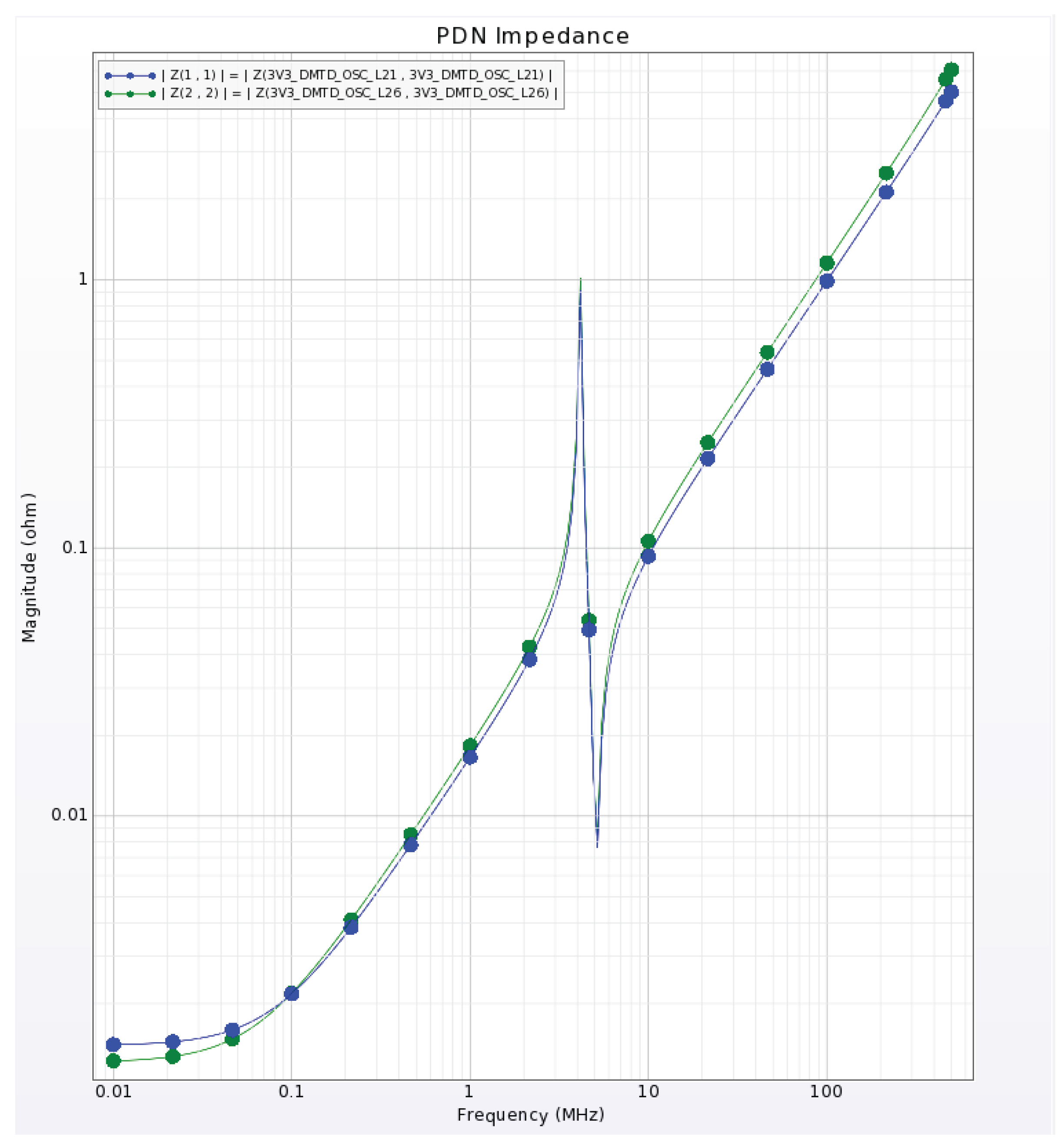
Figure 6.
Frequency-domain impedance profile of the DDMTD power distribution network (PDN) obtained through ADS simulation. Decoupling capacitor values and placements were optimized to maintain impedance below the target specification across the operating bandwidth, thereby minimizing simultaneous switching noise (SSN) and enhancing clock stability. The plot highlights resonance and anti-resonance points introduced by the distributed capacitor network, confirming compliance with high-speed mixed-signal design requirements.
4.2. Postlayout Power and Signal Integrity Simulations
Maintaining a consistently low power distribution network (PDN) impedance across the relevant frequency spectrum is a fundamental requirement for minimizing simultaneous switching noise (SSN) in high-speed digital and mixed-signal systems. This requirement becomes particularly critical when the PDN supplies precision clock generation circuits or oscillator networks, where any noise coupling through the PDN directly modulates the supply voltage. Such modulation manifests as additional phase noise and ultimately as jitter in the clock output signals. Even small perturbations on the supply rail can lead to measurable degradation in timing performance, especially when the jitter budget is stringent. When a transient current is drawn from the PDN during a switching event, it flows through the finite impedance of the network, producing a voltage fluctuation on the supply rail. Qualitatively, the peak-to-peak voltage excursion of SSN is proportional to both the magnitude of the transient current and the effective PDN impedance at the relevant frequency. Consequently, lowering PDN impedance is directly correlated with reducing SSN and improving overall power integrity. This relationship underpins the widespread use of target impedance specifications in high-performance designs. In this work, PDN impedance was extensively analyzed and optimized using Keysight ADS. A systematic approach was adopted to tune decoupling capacitor values, placement, and resonant frequency distribution, ensuring that the impedance profile remains below the target impedance across the bandwidth of interest. For this design, a target impedance of approximately at was established, corresponding to the maximum allowable voltage ripple that satisfies the oscillator’s supply tolerance. The effective bandwidth over which the PDN must remain below this target is determined by the frequency content of the transient current step response, which is related to the signal rise time. For a representative rise time of , the corresponding bandwidth extends to roughly , requiring low impedance up to and slightly beyond this range. The oscillator supply rails operate between and , imposing a tolerance of less than . Under the optimized PDN configuration, the maximum simulated voltage ripple was approximately , corresponding to about of the nominal supply voltage. This is well within allowable limits for stable oscillator operation and ensures that supply-induced jitter contributions remain negligible compared to other noise sources. Figure 7 and Figure 8 present the ADS simulation results, illustrating the impedance profile and voltage stability for the 3.3 V rail and the PDN of the linear regulator powering the clock circuitry. These simulations confirm compliance with design specifications and validate that voltage drops remain within acceptable limits under expected load conditions, thereby guaranteeing robust timing performance.
For additional validation, a conservative current ripple assumption of was considered to evaluate worst-case PDN performance. Under extreme conditions—where the supply voltage is at its minimum allowable value () and the maximum ripple is constrained to —the resulting equivalent impedance is approximately . This figure confirms that the optimized PDN design provides sufficient margin relative to the established target impedance of , ensuring robust power integrity even under unfavorable operating scenarios. The complete impedance profile, including resonances and anti-resonances introduced by the distributed capacitor network, was extracted through frequency-domain simulation and is presented in Figure 6. The results demonstrate that the impedance remains consistently below the target line across the entire frequency range of interest, with well-controlled resonance peaks and effective damping at critical frequencies. Overall, these findings highlight the importance of a systematic PDN design strategy—encompassing accurate capacitor selection, optimal physical placement to minimize loop inductance, and proper distribution of capacitance across multiple frequency decades. Such an approach effectively mitigates SSN and prevents clock jitter degradation, which is particularly crucial in mixed-signal systems where aggressive digital switching transients coexist with highly sensitive analog and timing circuits. By ensuring a stable supply environment, the PDN design directly contributes to maintaining low phase noise and preserving synchronization accuracy throughout the system.
The most signal-integrity-sensitive interconnects on the PCB are those associated with the oscillator subsystem, as they directly influence synchronization accuracy and jitter performance. Signal quality can be degraded by multiple factors, including connector discontinuities, dielectric substrate properties, parasitic elements in capacitors and packaged devices, and the physical layout and geometry of traces.
To quantify these effects, a widely adopted methodology involves the use of scattering parameters (S-parameters) [49]. This frequency-domain approach models interconnects as multi-port networks, capturing the interaction between incident and reflected voltage waves. For a two-port representation, the S-parameter is defined as the ratio of the voltage wave exiting at port m to the voltage wave incident at port n, i.e.,
In this context, characterizes reflection at port 1 due to an incident wave at the same port, while represents transmission from port 1 to port 2. The reflection coefficient can be expressed in decibels in terms of the load impedance and the characteristic impedance as:
The transmission parameter corresponds to insertion loss, which measures signal attenuation between input and output ports. Impedance mismatches increase insertion loss, and the longer the mismatched section, the greater the attenuation. Under well-matched conditions, dielectric loss dominates, while secondary effects such as coupling to adjacent traces, conductor resistance, and radiation are typically negligible. Energy conservation then implies:
which can be rewritten as:
This formalism extends naturally to differential signaling, where ports are treated as differential pairs. In such cases, mode conversion between differential and common modes occurs, leading to a mixed-mode S-parameter matrix. Here, SDD parameters describe transmission between differential-mode ports, SCC between common-mode ports, and SDC/SCD quantify conversions between differential and common modes. These mixed-mode parameters are essential for evaluating crosstalk and mode conversion in high-speed differential clock lines, ensuring that differential integrity is preserved throughout the PCB interconnect structure.
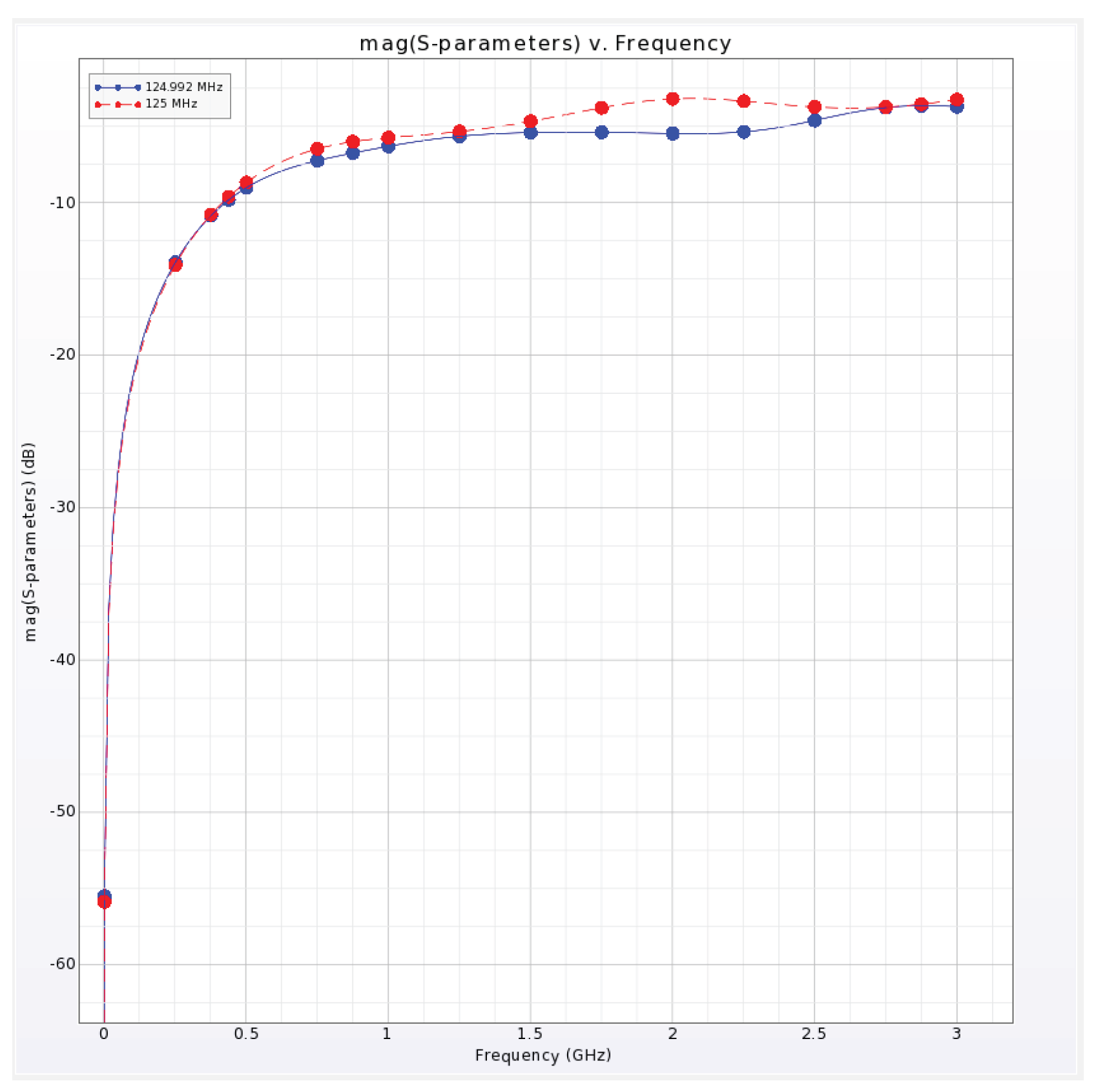
Using the design parameters described above, both return and insertion losses for the differential clock lines were simulated, with rise and fall times set to to represent realistic high-speed switching conditions. Figure 10 presents the insertion loss results for the differential clock distribution lines. Minimizing insertion loss is of primary importance, as excessive attenuation would directly increase timing jitter and compromise the ability of the system to maintain precise sub-nanosecond synchronization.
Figure 9.
Return loss simulation results, expressed as SDD11 parameters, for the 125 MHz and 124.992 MHz differential clock signals. The observed differences are primarily attributed to variations in PCB routing geometry and via transitions. Maintaining low return loss is essential to minimize signal reflections and ensure impedance matching, thereby preserving signal integrity and timing accuracy in high-speed clock distribution networks.
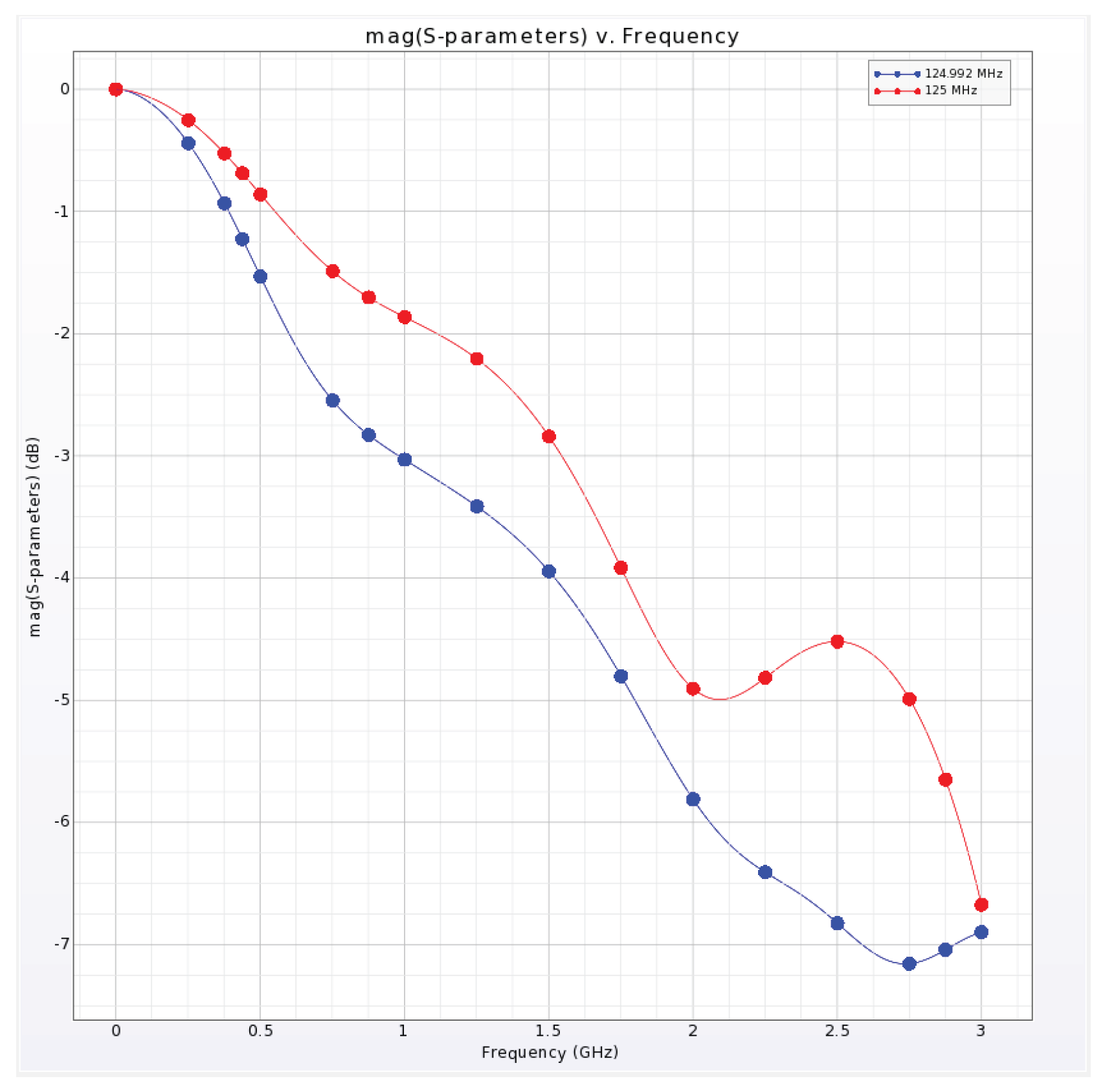
Figure 10.
Simulation results of insertion loss, expressed as SDD21 parameters, for the 125 MHz and 124.992 MHz differential clock lines. The observed variations between the two traces are primarily attributed to differences in PCB routing geometry and via transitions. Maintaining low insertion loss is critical to minimize signal attenuation and preserve timing accuracy in high-speed clock distribution networks.
Another critical factor that can degrade signal integrity is unwanted coupling between adjacent traces, primarily arising from parasitic capacitances and mutual inductances. This coupling generates induced voltages and noise on neighboring conductors, commonly referred to as victim lines. Depending on the observation point along the victim line, two main categories of crosstalk can be distinguished: Near-End Crosstalk (NEXT), appearing at the same end as the aggressor excitation, and Far-End Crosstalk (FEXT), appearing at the opposite end [50]. To assess these effects, simulations were performed between two representative differential pairs routed in close proximity and used for clock distribution. Since all clock pairs are designed with uniform spacing and geometry, the behavior of a single representative pair accurately reflects the overall design performance.
The simulation results of crosstalk are summarized in Figure 11 and Figure 12, showing both differential-to-differential mode coupling (SDD) and differential-to-common mode coupling (SCD). The induced noise levels remain close to , which is sufficiently low to ensure that clock integrity is preserved and that additional jitter contributions from coupling are negligible.
In addition, the characteristic impedance of the differential clock pairs was verified through simulation. The interconnects were designed with a target differential impedance of . For validation, the longest differential pairs were selected, as they represent the worst-case scenario for impedance control. The results, shown in Figure 13, confirm that impedance variations do not exceed , well within standard design tolerances for high-speed differential signaling. The localized peaks observed in the impedance profile are attributed to capacitive discontinuities introduced by vias at the line terminations. Importantly, these results are consistent with the pre-layout analysis presented in Figure 6, thereby validating both the design methodology and the simulation setup.
Finally, to directly evaluate the impact of the transmission line characteristics on timing precision, an eye-diagram analysis was performed. The eye diagrams of the differential clock lines, presented in Figure 14, exhibit a wide and clean eye opening, free from significant jitter or distortion. This confirms that the implemented routing strategy and impedance control are sufficient to preserve timing accuracy, thus ensuring the clock distribution network meets the stringent synchronization requirements of the system.
5. Conclusions and Future Work
The WR protocol requires specialized and highly precise hardware components to achieve its stringent synchronization performance. In this work, we have presented the design and development of an enhanced oscillator subsystem for the WRS, incorporating an additional redundant oscillator to improve system robustness and fault tolerance. Alongside the hardware design, a comprehensive signal integrity analysis was performed to evaluate the upgraded oscillator system under realistic operating conditions.
The results indicate that the phase noise levels of the oscillators are expected to remain well within acceptable thresholds, ensuring synchronization accuracy on the order of sub-nanoseconds. Furthermore, the analysis confirms that insertion loss, impedance variations, and crosstalk effects are sufficiently controlled to prevent any significant degradation in timing performance. These findings provide strong evidence that the proposed design meets the demanding requirements of WR applications.
Future work will focus on fabricating the revised board and conducting extensive experimental validation of both oscillator systems under practical conditions. This includes phase noise measurements, jitter characterization, and long-term stability tests within an improved version of the WRS. The outcomes of this effort will establish a highly reliable and precise timing solution, laying a solid foundation for next-generation distributed systems that demand deterministic synchronization at the sub-nanosecond level.
Acknowledgments
The authors acknowledge the support from MCIN for PID2021-124591NB-C41, -C42, -C43, PDI2024-156285NB-C41, -C42, -C43 and PDC2023-145913-I00 funded by MCIN/AEI/10.13039/501100011033 and by “ERDF A way of making Europe”, for ASFAE/2022/014 and ASFAE/2022/023 with funding from the EU NextGenerationEU (PRTR-C17.I01) and Generalitat Valenciana, for Grant AST22_6.2 with funding from Consejería de Universidad, Investigación e Innovación and Gobierno de España and European Union - NextGenerationEU, for CNS2023-144099, Generalitat Valenciana for CIDEGENT/2020/049, CIDEGENT/2021/23, CIDEIG/2023/20, ESGENT2024/24, CIPROM/2023/51, GRISOLIAP/2021/192 and INNVA1/2024/110 (IVACE+i), Spain;
References
- IEEE Std 1588-2019 (Revision ofIEEE Std 1588-2008); Synchronization Distribution in 5G Transport Networks. 2022.
- Venmani, D.; Lagadec, Y.; Lemoult, O.; Deletre, F. Phase and Time Synchronization for 5G C-RAN: Requirements, Design Challenges and Recent Advances in Standardization. EAI Endorsed Transactions on Industrial Networks and Intelligent Systems 2018, 5, 155238. [Google Scholar] [CrossRef]
- Li, H.; Han, L.; Duan, R.; Garner, G.M. Analysis of the Synchronization Requirements of 5g and Corresponding Solutions. IEEE Communications Standards Magazine 2017, 1, 52–58. [Google Scholar] [CrossRef]
- Rokui, R.; et al. Synchronization Requirements in 5G Massive MIMO Systems. IEEE Transactions on Wireless Communications 2019, 18, 3215–3228. [Google Scholar]
- Geng, Y.; Liu, S.; Yin, Z.; Naik, A.; Prabhakar, B.; Rosenblum, M.; Vahdat, A. Exploiting a Natural Network Effect for Scalable, Fine-grained Clock Synchronization. In Proceedings of the Symposium on Networked Systems Design and Implementation, 2018. [Google Scholar]
- Stathakopoulou, C.; et al. Sync HotStuff: Blockchain Synchronization via Pipelined BFT. ACM SIGOPS Operating Systems Review 2022, 56, 31–37. [Google Scholar]
- Ageron, M.; et al. ANTARES: the first undersea neutrino telescope. Nucl. Instrum. Meth. A 2011, arXiv:astro656, 11–38. [Google Scholar] [CrossRef]
- Adrian-Martinez, S.; et al. Letter of intent for KM3NeT 2.0. J. Phys. G 2016, arXiv:astro43, 084001. [Google Scholar] [CrossRef]
- Aartsen, M.G.; et al. The IceCube Neutrino Observatory: Instrumentation and Online Systems. JINST 2017, arXiv:astro12, P03012. [Google Scholar] [CrossRef]
- Andres, E.; et al. The AMANDA neutrino telescope: Principle of operation and first results. Astropart. Phys. 2000, 13, 1–20, [astro-ph/9906203. [Google Scholar] [CrossRef]
- Malyshkin, Y. Baikal-GVD neutrino telescope: Design reference 2022. Nucl. Instrum. Meth. A 2023, 1050, 168117. [Google Scholar] [CrossRef]
- Perlin, M. Particle Physics with the Pierre Auger Observatory. SciPost Phys. Proc. 2022, arXiv:astro8, 130. [Google Scholar] [CrossRef]
- Terzian, Y.; Lazio, J. The Square Kilometre Array. Proc. SPIE Int. Soc. Opt. Eng. 2006, 6267, 62672D. [Google Scholar] [CrossRef]
- as listed in the paper, A. Title of the paper from the PDF. EPJ Web of Conferences 2025, 302, 12011.
- Ferrini, F.; Wild, W. The Cherenkov Telescope Array Observatory Comes of Age. ESO Messenger 2020, 180, 3–8. [Google Scholar] [CrossRef]
- Deller, A.; et al. SKA Observatory Technical Report SKA-TRN-113; Timing and Synchronization Requirements for the SKA Phase 2. 2023.
- Alvarez, P.; et al. White Rabbit Deployment in CERN’s LHC Timing System. IEEE Transactions on Nuclear Science 2023, 70, 712–719. [Google Scholar]
- Lipinski, M.; Wlostowski, T.; Serrano, J.; Alvarez, P. White rabbit: a PTP application for robust sub-nanosecond synchronization 2011, 10, 25–30. [CrossRef]
- White Rabbit PTP Core. 28 02 2023. Available online: https://ohwr.org/projects/wr-cores/wiki/wrpc-core.
- Technology, M. MT-085: Ultra-Stable Oven-Controlled Oscillator, 2023. DS60001542B.
- Zhang, L.; et al. High-Speed PCB Design Techniques for Sub-Nanosecond Systems. IEEE Transactions on Electromagnetic Compatibility 2021, 63, 1234–1242. [Google Scholar]
- White Rabbit Collaboration. 28 02 2023. Available online: https://www.white-rabbit.tech/.
- Serrano, J.; et al. White Rabbit Project. Proceedings of ICALEPCS2009, Kobe, Japan, 2009; pp. 93–95. [Google Scholar]
- Lipinski, M.; Wlostowski, T.; Serrano, J.; Alvarez, P. White rabbit: a PTP application for robust sub-nanosecond synchronization. 2011 IEEE International Symposium on Precision Clock Synchronization for Measurement, Control and Communication; 2011; pp. 25–30. [Google Scholar]
- IEEE Std 1588-2008 (Revision of IEEE Std 1588-2002)2008; IEEE Standard for a Precision Clock Synchronization Protocol for Networked Measurement and Control Systems. pp. 1–269. [CrossRef]
- Lan, Y.K.; Chen, Y.S.; Hou, T.C.; Wu, B.L.; Chu, Y.S. Development Board Implementation and Chip Design of IEEE 1588 Clock Synchronization System Applied to Computer Networking. Electronics 2023, 12. [Google Scholar] [CrossRef]
- Timing characteristics of synchronous ethernet equipment slave clock. 2007.
- IEEE Standard for a Precision Clock Synchronization Protocol for Networked Measurement and Control Systems. IEEE Std 1588-2019 (Revision ofIEEE Std 1588-2008) 2020, 1–499. [CrossRef]
- Li, F.; Liu, W.; Qi, Y.; Li, Q.; Liu, G. An Enhanced Method for Nanosecond Time Synchronization in IEEE 1588 Precision Time Protocol. Processes 2023, 11. [Google Scholar] [CrossRef]
- Bielewicz, M.; Bancer, A.; Dziedzic, A.; Grzyb, J.; Jaworska, E.; Kasprowicz, G.; Kiecana, M.; Kolasinski, P.; Kuc, M.; Kuklewski, M.; et al. Practical Implementation of an Analogue and Digital Electronics System for a Modular Cosmic Ray Detector. Electronics 2023, 12. [Google Scholar] [CrossRef]
- Aiello, S.; et al. KM3NeT front-end and readout electronics system: hardware, firmware and software. J. Astron. Telesc. Instrum. Syst. 2019, arXiv:astro5, 046001. [Google Scholar] [CrossRef]
- Vella Wallbank, J.; Amodeo, M.; Beaumont, A.; Buzio, M.; Di Capua, V.; Grech, C.; Sammut, N.; Giloteaux, D. Development of a Real-Time Magnetic Field Measurement System for Synchrotron Control. Electronics 2021, 10. [Google Scholar] [CrossRef]
- Jones, T.; Arnold, D.; Tuffner, F.; Cummings, R.; Lee, K. Recent Advances in Precision Clock Synchronization Protocols for Power Grid Control Systems. Energies 2021, 14. [Google Scholar] [CrossRef]
- Nabwani, M.; Suleymanov, M.; Pinhasi, Y.; Yahalom, A. Real-Time Fault Location Using the Retardation Method. Electronics 2022, 11. [Google Scholar] [CrossRef]
- Rifandi, R.; Assagaf, S.; Ningtyas, Y.D.W.K. An Insight About GPS; 2013. [Google Scholar] [CrossRef]
- Lee, J. Global positioning/GPS; 2009; pp. 548–555. [Google Scholar] [CrossRef]
- Moreira, P.; Alvarez, P.; Serrano, J.; Darwezeh, I.; Wlostowski, T. Digital dual mixer time difference for sub-nanosecond time synchronization in Ethernet. In Proceedings of the 2010 IEEE International Frequency Control Symposium, 2010; pp. 449–453. [Google Scholar] [CrossRef]
- Hennig, W.; Hoover, S. White Rabbit Time Synchronization for Radiation Detector Readout Electronics. IEEE Transactions on Nuclear Science 2020, 68, 2059–2065. [Google Scholar] [CrossRef]
- Rogers, B.M. Virtual prototyping and concurrent engineering in PCB manufacturing. IEEE Transactions on Electronics Packaging Manufacturing 1997, 20, 300–308. [Google Scholar]
- Zainudeen, P.B.; Althari, A.; Iqbal, M.T. A survey on virtual prototyping tools for PCB design. In Proceedings of the 2018 International Conference on Innovative Trends in Computer Engineering (ITCE), Aswan 2018; pp. 93–98. [Google Scholar]
- Muir, D.; Panicker, R. The use of virtual prototyping in PCB design. In Proceedings of the 2015 IEEE MTT-S International Microwave Workshop Series on Advanced Materials and Processes for RF and THz Applications (IMWS-AMP), Suzhou, 2015; pp. 1–3. [Google Scholar] [CrossRef]
- Chen, J.Y.; Liu, K.S.; Huang, C.M. Virtual prototyping for signal integrity analysis of high-speed PCBs. IEEE Transactions on Electromagnetic Compatibility 2006, 48, 711–720. [Google Scholar]
- Silaghi, A.M.; Pescari, C.; Bleoju, C.; De Sabata, A. Solving Automotive Signal Integrity Issues by EMC Simulation. In Proceedings of the 2021 IEEE 27th International Symposium for Design and Technology in Electronic Packaging (SIITME), 2021; pp. 33–36. [Google Scholar] [CrossRef]
- Silaghi, A.M.; Mueller, F.; De Sabata, A.; Buta, A.P.; Nicolae, P.M. Analysis of Shielding Effectiveness of an Automotive Display through Simulation and Testing. In Proceedings of the 2020 International Symposium on Electromagnetic Compatibility-EMC EUROPE. IEEE, 2020; pp. 1–4. [Google Scholar]
- Silaghi, A.M.; De Sabata, A. EMC Simulation of an Automotive Ethernet Interface. In Proceedings of the 2020 International Symposium on Electronics and Telecommunications (ISETC), 2020; IEEE; pp. 1–4. [Google Scholar]
- Behagi, A. RF and Microwave Circuit Design: A Design Approach Using (ADS); Advanced design system. Techno Search 2015. [Google Scholar]
- Behagi, A. 100 RF and Microwave Circuit Design: With Keysight (ADS) Solutions; Techno Search, 2018. [Google Scholar]
- Johnson, H.; Graham, M. High-speed Digital Design: A Handbook of Black Magic; Prentice Hall Modern Semiconductor Design, Prentice Hall, 1993. [Google Scholar]
- Bogatin, E. Signal and Power Integrity–simplified; Prentice Hall PTR Signal Integrity Library, Prentice Hall, 2010. [Google Scholar]
- Mudavath, R.; Naik, B.R. Estimation of Far End Crosstalk and Near End Crosstalk Noise with Mutually Coupled RLC Interconnect Models. In Proceedings of the 2018 International Conference on Communication and Signal Processing (ICCSP), 2018; pp. 182–185. [Google Scholar] [CrossRef]
Figure 1.
Cross-sectional stack-up of the SCB, illustrating the twelve copper and dielectric layers used in its construction. The design employs FR-4 as the primary dielectric material, ensuring mechanical stability and electrical insulation between layers. This view provides insight into the board’s multilayer architecture, which supports high-density routing and signal integrity for complex electronic systems.
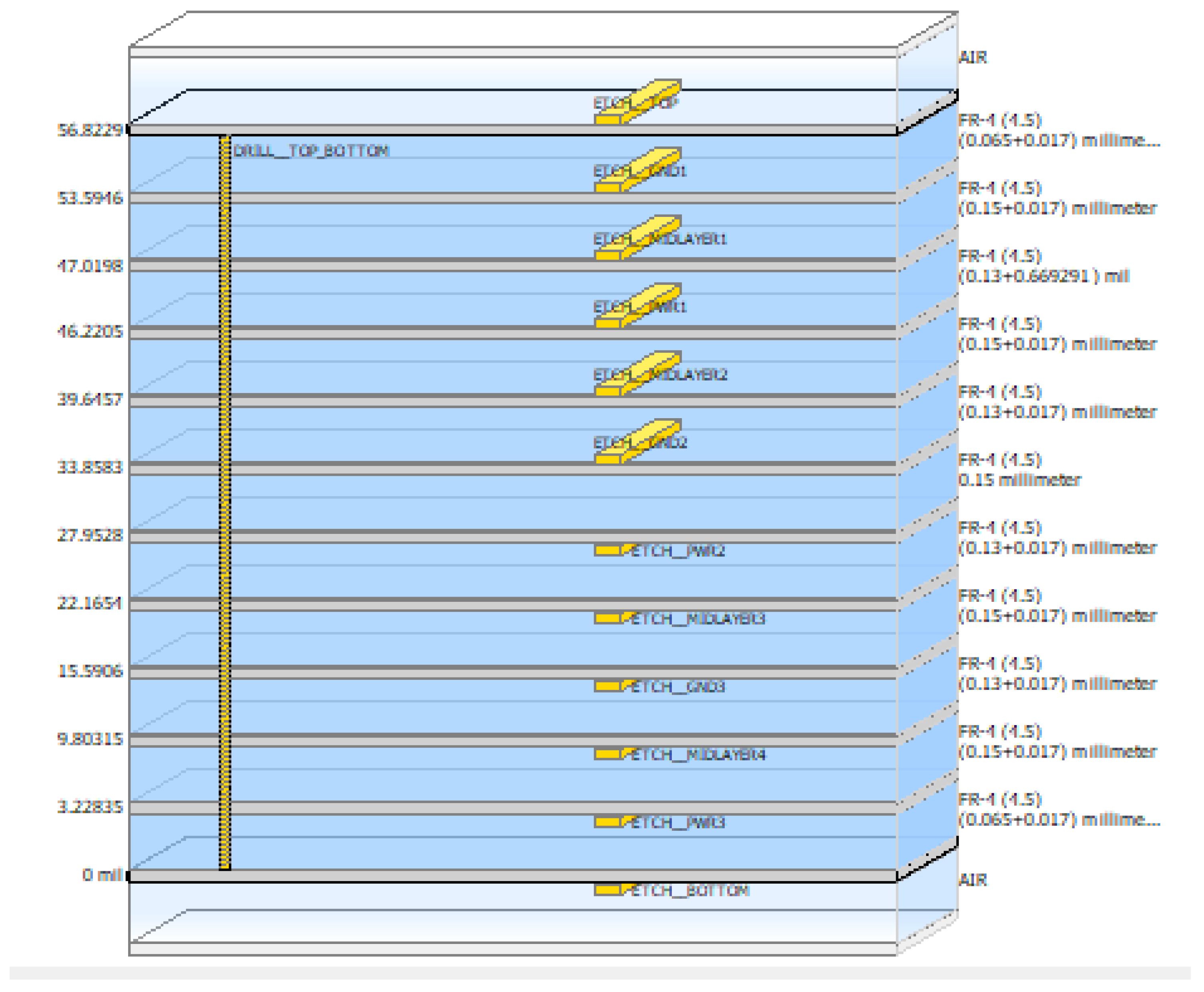
Figure 2.
Three-dimensional perspective of the top layer of the SCB, showing the placement of components, connectors, and routing as designed in Altium Designer. This view highlights the mechanical arrangement and spatial distribution of elements, providing a clear visualization of the board’s layout for assembly and inspection purposes.
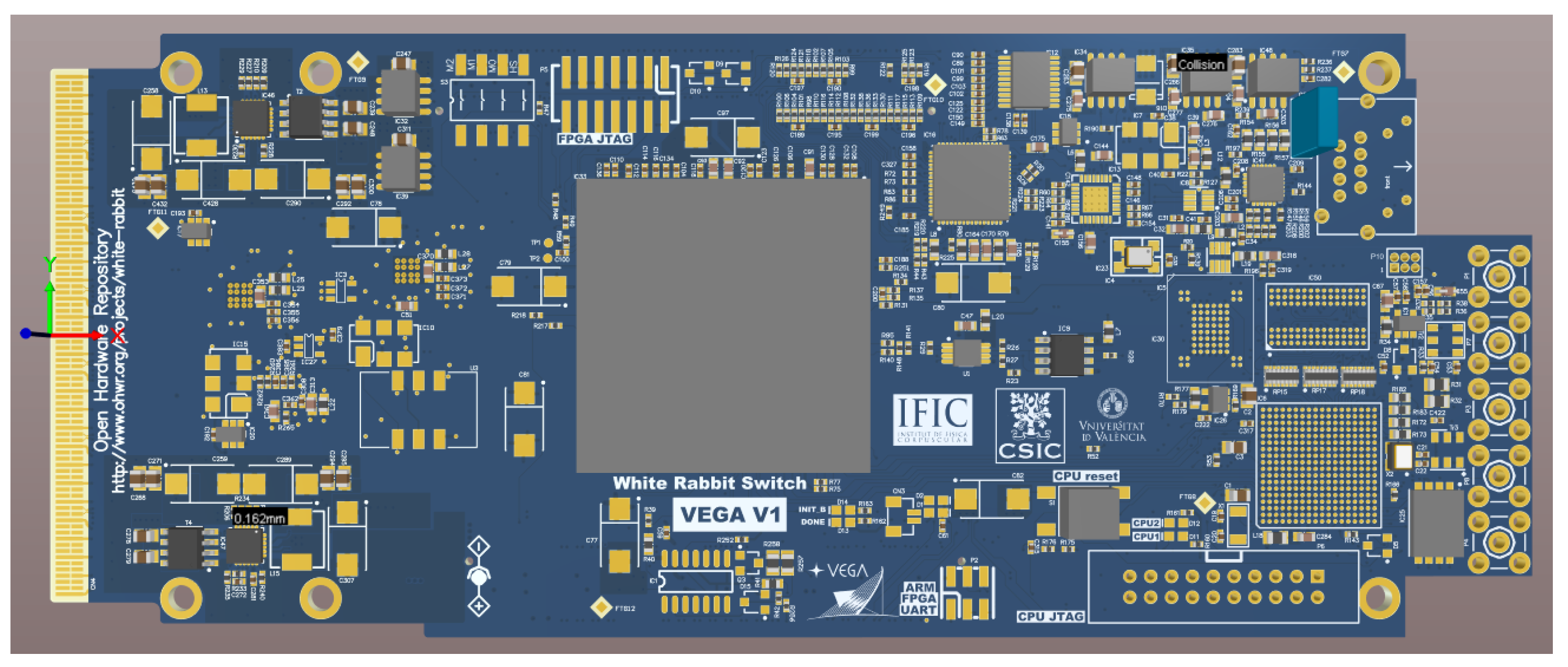
Figure 3.
3D View of the bottom of the SCB, taken from Altium Designer software
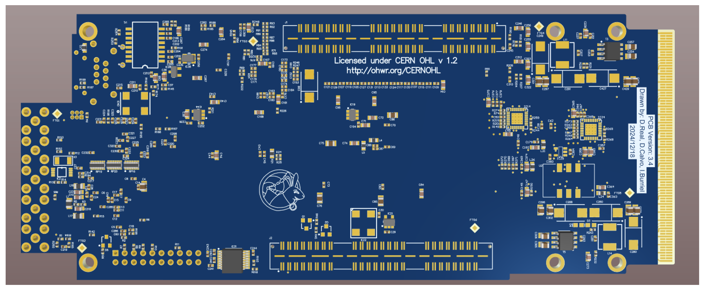
Figure 4.
Simulation of the trace geometry to achieve a 100 Ω differential impedance. For internal traces, a fixed separation of 0.265 mm was used while sweeping the width from 0.05 mm to 0.15 mm. For external traces, a width of 0.1 mm was selected. All simulations were conducted using ADS.
Figure 4.
Simulation of the trace geometry to achieve a 100 Ω differential impedance. For internal traces, a fixed separation of 0.265 mm was used while sweeping the width from 0.05 mm to 0.15 mm. For external traces, a width of 0.1 mm was selected. All simulations were conducted using ADS.
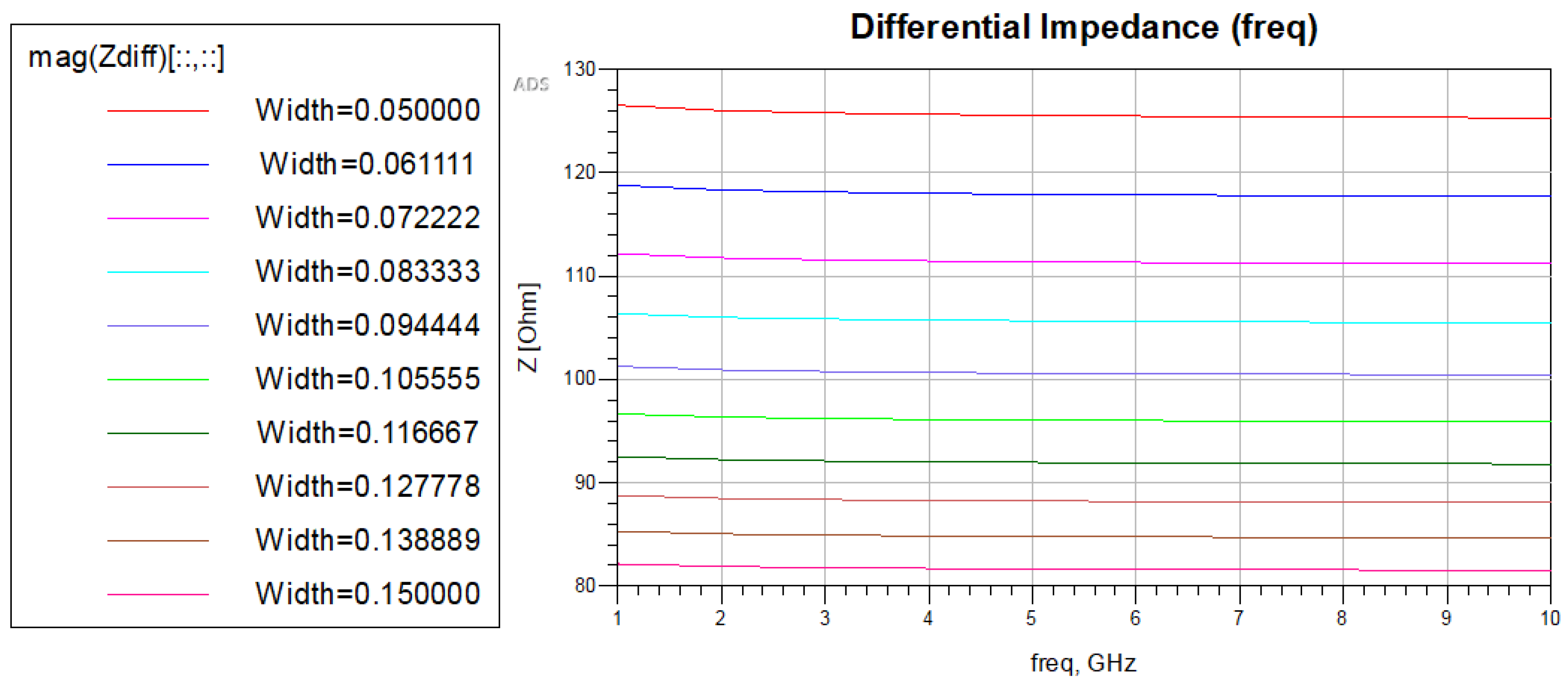
Figure 5.
Left: 3D model illustrating the via structure and surrounding antipad configuration within the PCB stack-up. Right: Electromagnetic simulation results validating the antipad geometry for maintaining a 100 Ω differential impedance across high-speed LVDS clock lines. The analysis accounts for parasitic effects introduced by via barrels and copper clearances, ensuring impedance continuity through inter-layer transitions.
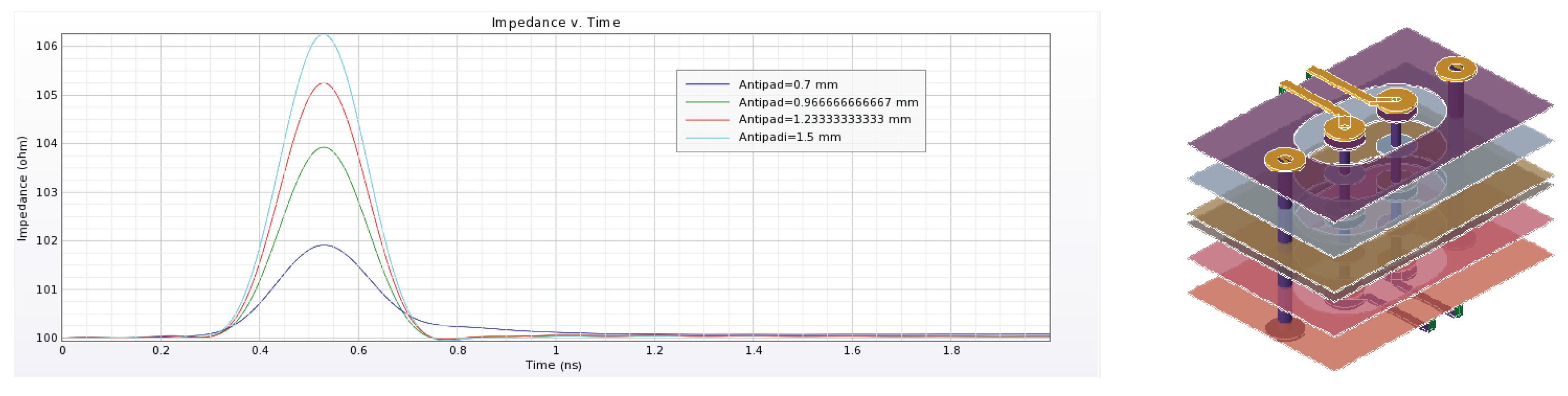
Figure 7.
ADS simulation of voltage stability along the 3.3 V main power rail. The results show a minimal variation, with the voltage ranging from 3.299 V to 3.300 V, indicating an almost negligible drop and confirming excellent stability in the primary power distribution network. This performance ensures reliable operation of the clock generation circuitry and validates the effectiveness of the PDN design under dynamic load conditions.
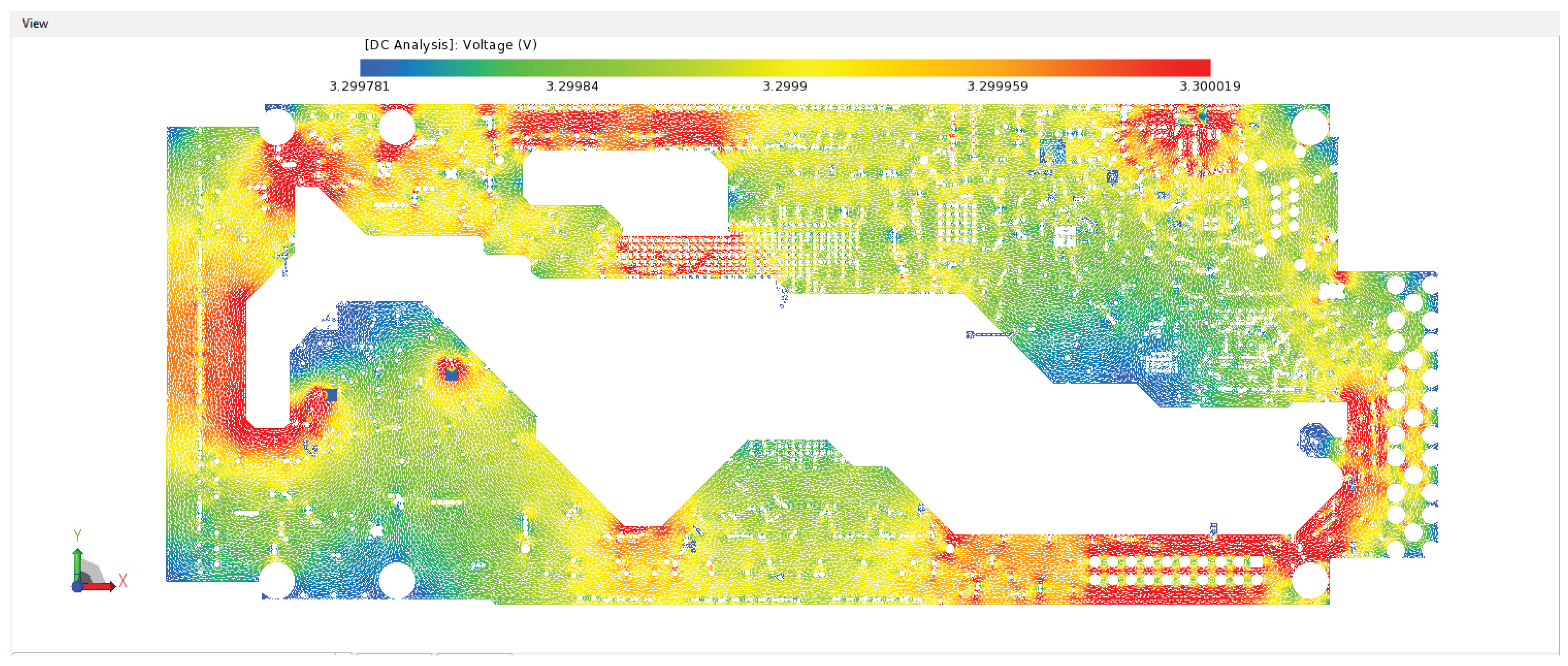
Figure 8.
ADS simulation of the voltage stability in the 3.3 V linear regulator supplying the clock generation circuitry. The output voltage varies between 3.268 V and 3.297 V under dynamic load conditions, indicating a slightly larger drop compared to the main rail but remaining well within acceptable limits for reliable oscillator operation. This analysis validates the regulator’s performance and suitability for maintaining power integrity in the clock distribution network.
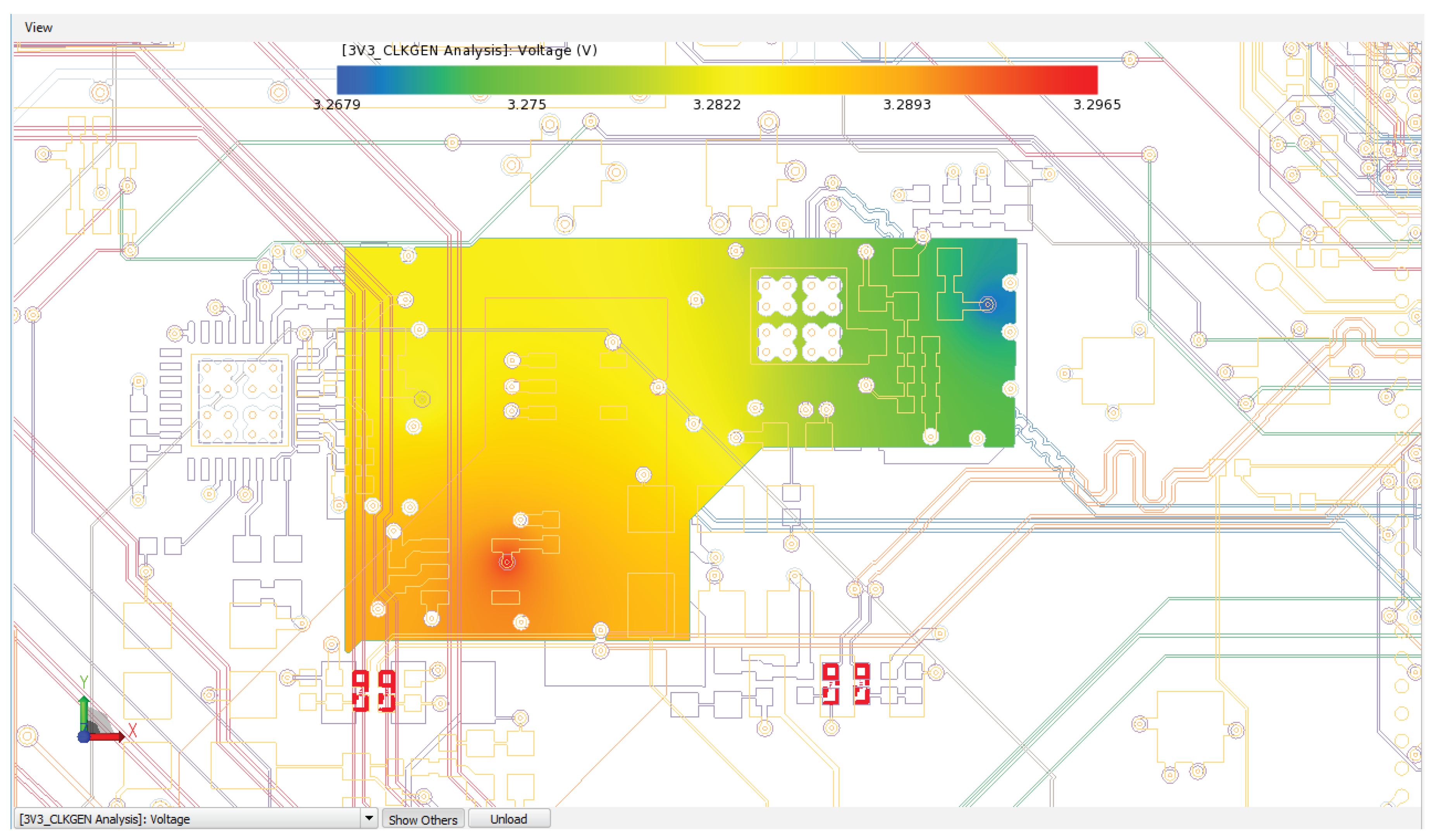
Figure 11.
Simulation of FEXT crosstalk noise—both differential and common mode—between two neighboring differential signal pairs.
Figure 11.
Simulation of FEXT crosstalk noise—both differential and common mode—between two neighboring differential signal pairs.
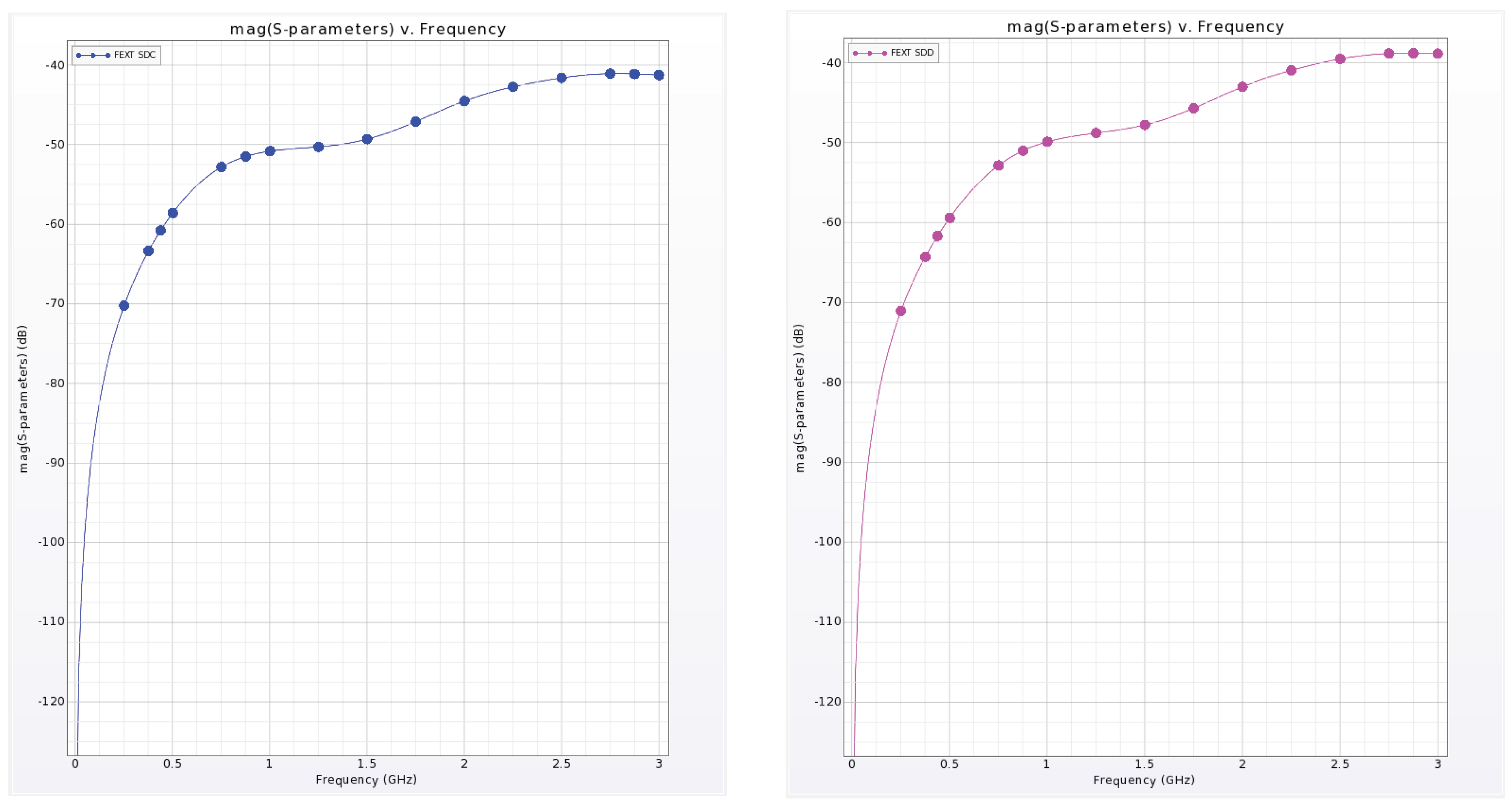
Figure 12.
Near-End Crosstalk (NEXT) analysis between two adjacent differential signal pairs, evaluated in both differential and common modes. The results quantify electromagnetic coupling effects at the point of signal injection, highlighting their impact on signal integrity, timing accuracy, and noise margins in high-speed PCB designs.
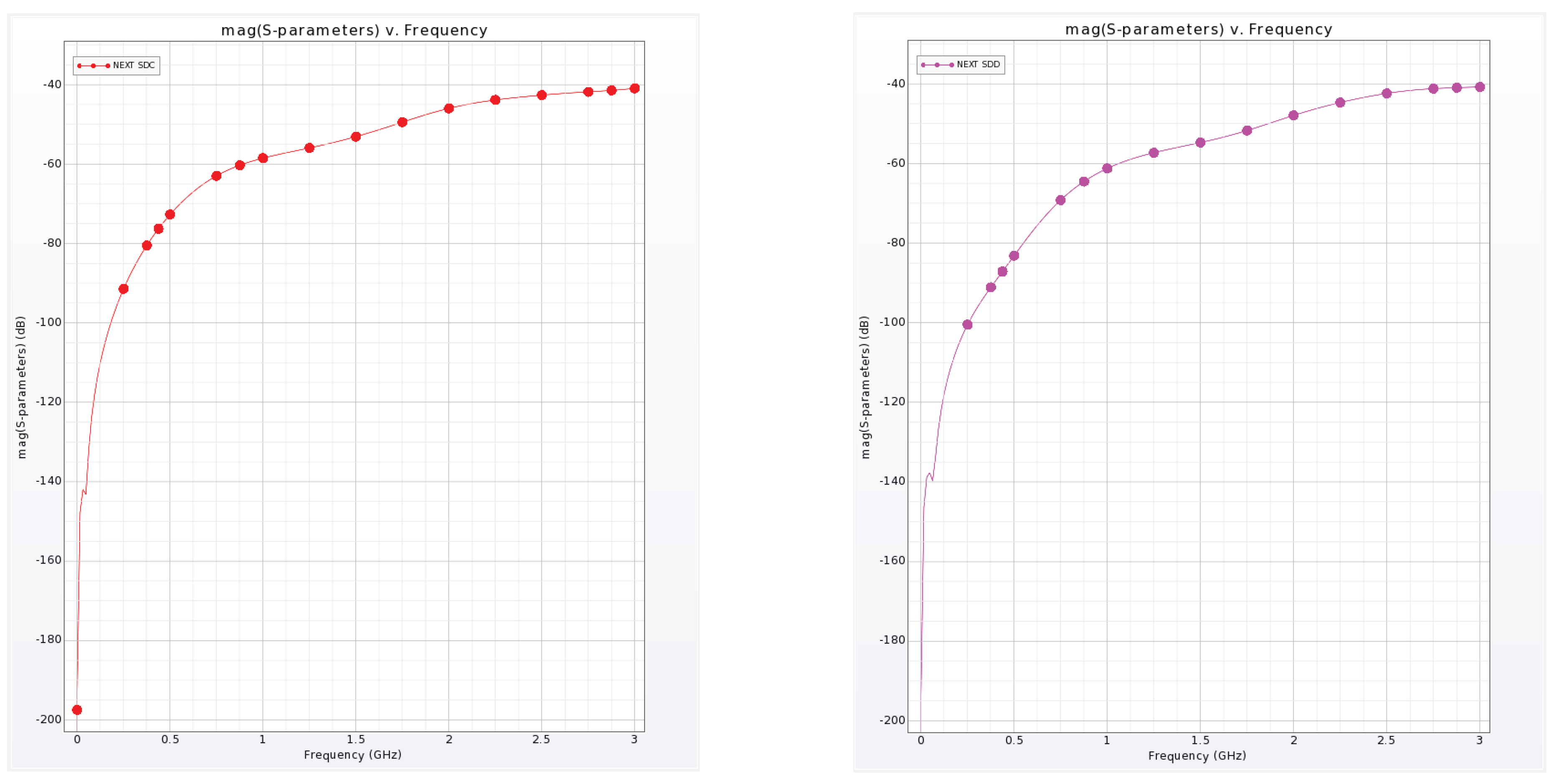
Figure 13.
Simulation of the characteristic impedances of the longest differential pairs carrying clock signals. The significant negative dips in the graph are due to capacitive effects introduced by the connector termination points at the ends of the lines.
Figure 13.
Simulation of the characteristic impedances of the longest differential pairs carrying clock signals. The significant negative dips in the graph are due to capacitive effects introduced by the connector termination points at the ends of the lines.
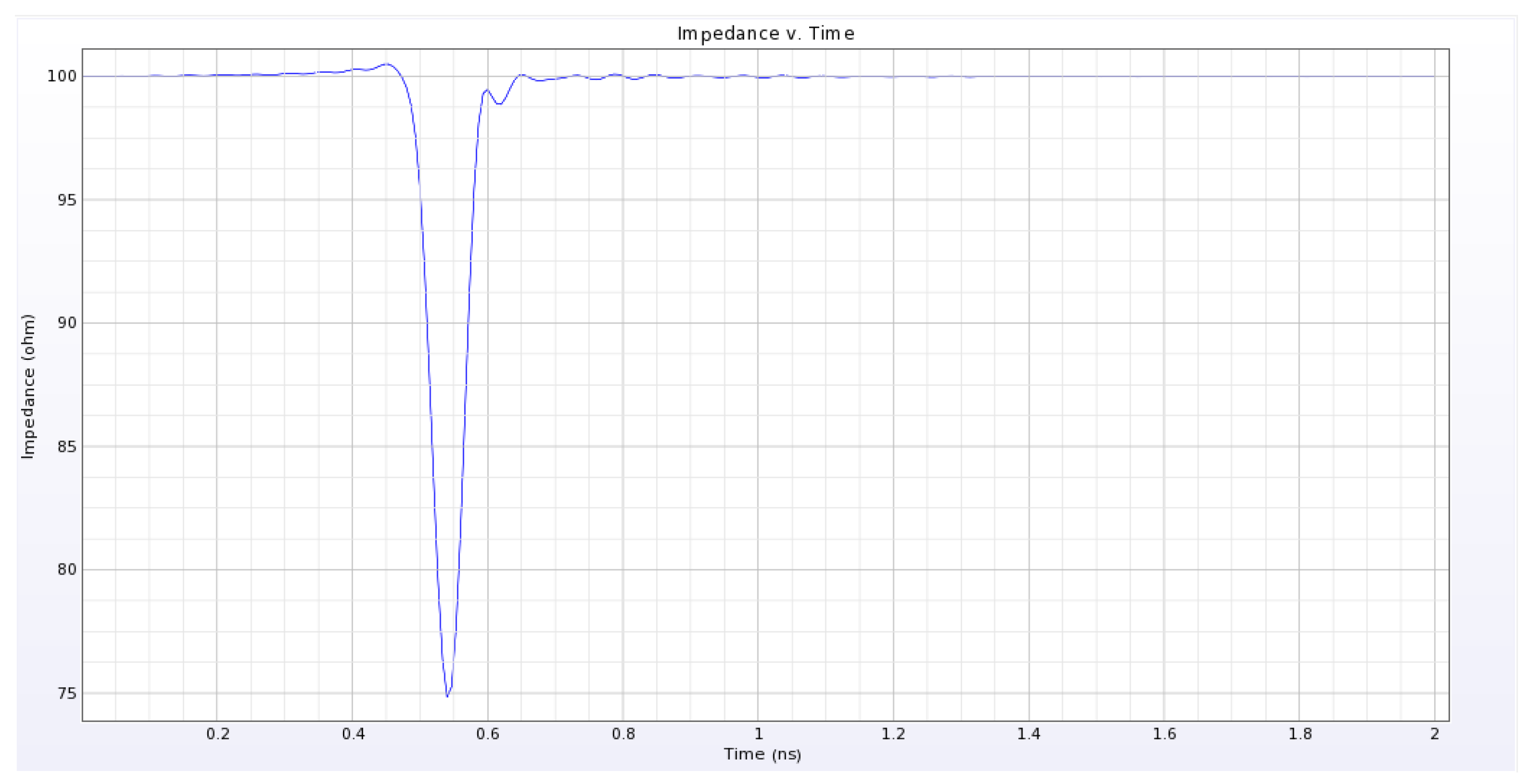
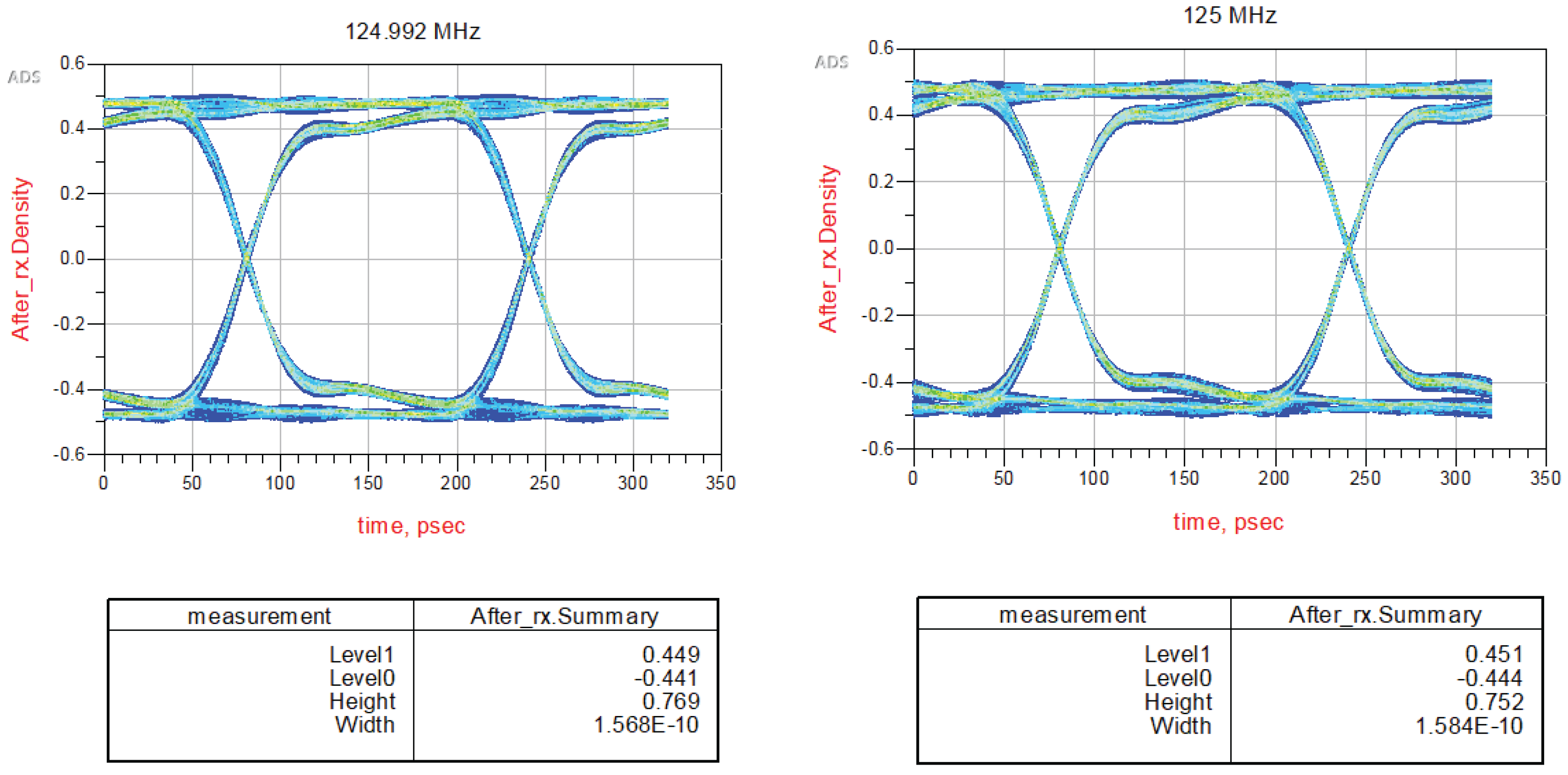
Figure 14.
Eye diagram results for the 125 MHz and 124.992 MHz differential clock lines. Both diagrams exhibit eye openings exceeding 80% of the unit interval (UI), indicating excellent signal integrity and minimal jitter. The wide eye aperture confirms that the implemented routing strategy and impedance control effectively preserve timing accuracy, ensuring compliance with the stringent synchronization requirements of the WR protocol.
Disclaimer/Publisher’s Note: The statements, opinions and data contained in all publications are solely those of the individual author(s) and contributor(s) and not of MDPI and/or the editor(s). MDPI and/or the editor(s) disclaim responsibility for any injury to people or property resulting from any ideas, methods, instructions or products referred to in the content. |
© 2026 by the authors. Licensee MDPI, Basel, Switzerland. This article is an open access article distributed under the terms and conditions of the Creative Commons Attribution (CC BY) license (http://creativecommons.org/licenses/by/4.0/).
Copyright: This open access article is published under a Creative Commons CC BY 4.0 license, which permit the free download, distribution, and reuse, provided that the author and preprint are cited in any reuse.


