
Submitted:
10 December 2025
Posted:
11 December 2025
You are already at the latest version
Abstract
Deep Reactive Ion Etching (DRIE), as a key process in silicon micromachining, remains constrained in high-precision applications by sidewall angle deviation and aspect ratio limitations. This study systematically investigates the mapping relationship between process parameters and etching morphology, focusing on: The influence mechanism of C₄F₈ passivation time and bottom RF power on sidewall perpendicularity The effect patterns of etch cycle count, single-step time, and bottom RF power on aspect ratio and top-bottom line width (CD) difference Findings reveal: Dynamic adjustment of bottom RF power significantly influences sidewall angle. Incremental adjustment tends to cause sharp angles (decreased angular precision), while decremental adjustment tends to form obtuse angles. Simply increasing cycle count leads to a bottleneck in etch depth growth. Combining incremental bottom RF power adjustment can overcome depth limitations but induces axial variation in aperture dimensions. Optimizing the pas-sivation-etch time ratio effectively controls etch morphology characteristics. This study achieved an etch depth of 112.2 μm for a 5 μm wide trench with an overall ap-erture size difference of 0.279 μm, providing a theoretical basis and practical guidance for parameter optimization in DRIE processes for high-precision silicon structure fab-rication.
Keywords:
sidewall
; single-step time
; RF power
; top-bottom line width
; passivation-etch time ratio
1. Introduction
As a core technology comprising etching and passivation cycles, the Bosch process holds a pivotal position in the fabrication of high aspect ratio silicon microstructures [1,2,3]. However, this process faces dual challenges in practice: On one hand, achieving anisotropic etching with vertical sidewall angles while maintaining consistent trench opening dimensions remains an industry-wide challenge [4,5]; On the other hand, micro-scale pattern etching is constrained by etch depth (or aspect ratio)—as the number of etch cycles increases, reactive ions and gases struggle to diffuse into confined effectively etch regions, directly limiting process performance improvements [6].
The root cause of these issues lies in the complexity of the process system: within each etching/passivation cycle, multiple parameters—including chamber pressure, etching/passivation gas flow rates, the etching-to-passivation time ratio, substrate temperature, center RF power, and bottom RF power—must be precisely controlled to establish a balanced process system [7,8,9,10]. Only through such precise control can effective regulation of etch dimensions and aspect ratio be achieved, while simultaneously ensuring consistency in silicon trench aperture size and verticality of sidewalls [11,12].
To overcome these limitations, research has focused on optimizing DRIE process parameters for micro-scale patterns, aiming to improve etch profiles and enhance etch depth [13,14,15]. For example, research has achieved TSV hole etching with a diameter of 50 μm and a depth of 300 μm. [16]. Exploration of Bosch processes with aspect ratios ranging from 3:1 to 7.5:1 revealed that controlling anisotropy and roughness becomes exceptionally challenging when the aspect ratio exceeds 15 [17]. In studies of 15μm diameter hole arrays, aspect ratios as high as 26 have been achieved [18]. However, investigations into smaller dimensions reveal that the aspect ratio of the optimized 4 μm diameter holes can reach 12.5 [19,20], their cross-sectional area decreases with increasing aspect ratio, resulting in a bottom dimension less than half that of the top.
It is evident that for deep etching of microstructures related to Bosch processes, particularly in scenarios involving small apertures, a comprehensive understanding of the deep silicon etching mechanism under conditions of vertical sidewall angle and trench aperture size consistency holds critical practical significance.
Given this, this study proposes an optimized method for small-aperture etching, focusing on improving aspect ratio and uniformity of trench aperture size. Through systematic investigation of the effects of Bosch process cycles and bottom radiofrequency power on etch depth, anisotropy, sidewall angle, and aperture size uniformity, an experimental analysis-based silicon etching equilibrium model is established. This provides a universal technical solution for deep etching in the fabrication of silicon microstructures.
2. Materials and Methods
Spin-coat 4620 photoresist onto a 4-inch silicon wafer oriented along the <100> crystal direction, achieving a film thickness of 6 μm. Form the etching pattern via UV exposure, with feature dimensions of 5–25 × 5000 μm as shown in Figure 1a. Subsequently, etch the sample using a three-step Bosch process. First, the base recipe specified in Table 1 was employed, with parameters including etch cycle count, bottom RF power, C4F8 introduction time and flow rate, and SF6 introduction time. Standard process results are shown in Figure 1b. Using these parameters for etching, the etch depth-to-width ratio was enhanced by varying the etch cycle count, C4F8 introduction time, C4F8 gas flow rate, SF6 introduction time, and bottom RF power to observe the results [21].
3. Results
The optimized Bosch process comprises three steps: first, passivation with C₄F₈ [22,23,24,25]; second, opening the passivation layer via high-energy bombardment with SF₆; third, etching through chemical reaction between SF₆ and Si. During the first deposition step, fluorocarbon compounds form on the bottom and sidewalls to provide protection. In the second step, high RF power at the bottom creates strong ion traction, physically bombarding the passivation layer to open it for chemical etching in the third step. Chemical etching can be categorized into two types: spontaneous isotropic etching of F* groups and ion-enhanced F* group etching. The four process parameters studied in this paper are divided into two parts: the number of etching cycles, the introduction time and flow rate of C4F8, and the introduction time of SF6, which influence the final etching morphology through chemical reactions. Meanwhile, the bottom RF power primarily affects the etching morphology through physical bombardment. The etching parameters are shown in Table 2.
Directly correlated with etch depth is the number of etch cycles. As the number of etch cycles increases, the etch depth correspondingly increases. Therefore, three sets of experiments were conducted with the number of etch cycles as the variable.
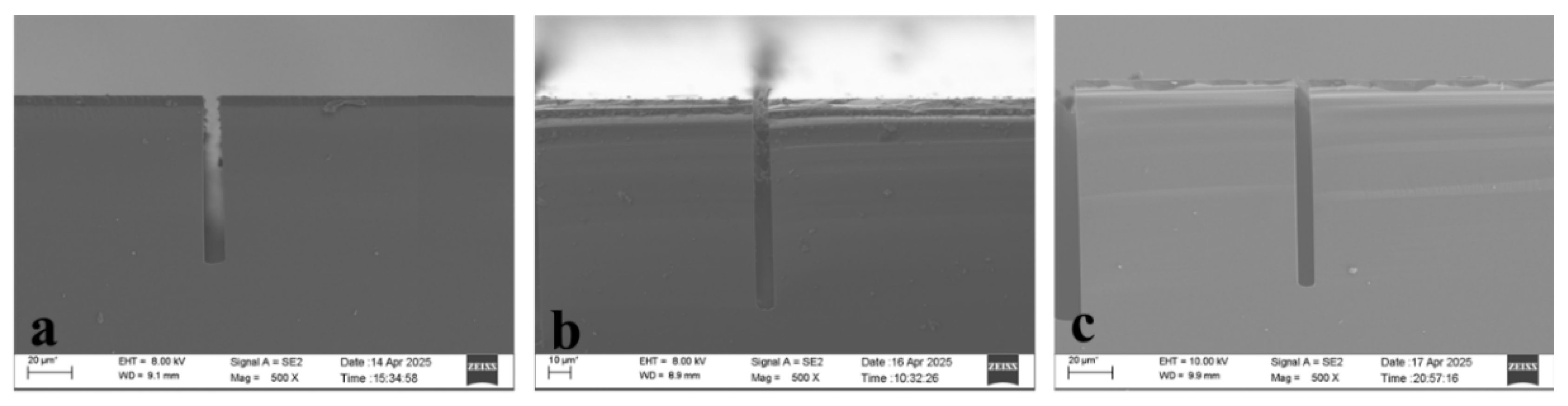
After 100 etching cycles, the etching depth of a 5μm-wide trench reached 77.49μm. When the number of etching cycles was increased to 150, the etching depth reached 96.24 μm. Further increasing the cycles to 180 yielded an etching depth of 95.57 μm, which was close to the depth achieved at 150 cycles. This demonstrates that simply increasing the number of etching cycles does not lead to further increases in etching depth. This is because the small aperture area gas replacement becomes insufficiently rapid. Once etching reaches a certain depth, gas cannot continue to propagate downward, causing the etch depth to plateau at a threshold when cycles are increased further.
Figure 2.
(a, b, c) show SEM images after 100, 150, and 180 etching cycles, respectively.
To enable gas penetration to deeper etching regions, we devised two approaches: one involves increasing the bottom RF power to enhance the bottom's attraction to ions, allowing them to reach the etching bottom and continue downward etching; the other extends the etching gas introduction time to increase ion concentration, thereby promoting downward etching. Consequently, the following experiments were conducted.
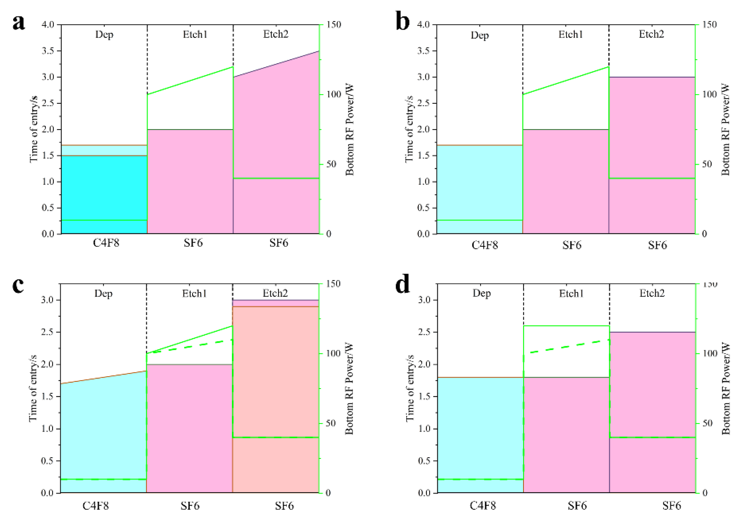
Figure 3.
Etching parameter diagram. (a) Blue bars represent C4F8 introduction time (lighter blue indicates the second experimental group, identical to the first group except for this variable); pink bars denote SF6 introduction time for steps two and three; green dashed line shows bottom RF power level. (b) Blue bars represent C4F8 introduction time; pink bars represent SF6 introduction time in the second and third steps; green dashed line indicates bottom RF power level; (c) Blue bars represent C4F8 introduction time; pink bars represent SF6 introduction time in the second and third steps (orange indicates variables for the second experimental group); green dashed line indicates bottom RF power level (dashed line indicates variables for the second experimental group); (d) Blue bars represent C4F8 introduction time, pink bars indicate SF6 introduction time for the second and third steps, and the green dashed line shows bottom RF power level (dashed line denotes the second set of experimental variables);.
As etch depth increased, both etch gas flow time and bottom RF power were ramped up. When the chemical etch time was adjusted from a constant 3 seconds to 3.5 seconds as the number of etch cycles increased, and the bottom RF power was increased from 100W to 120W over the same number of cycles, the etch depth reached 114.3 μm.
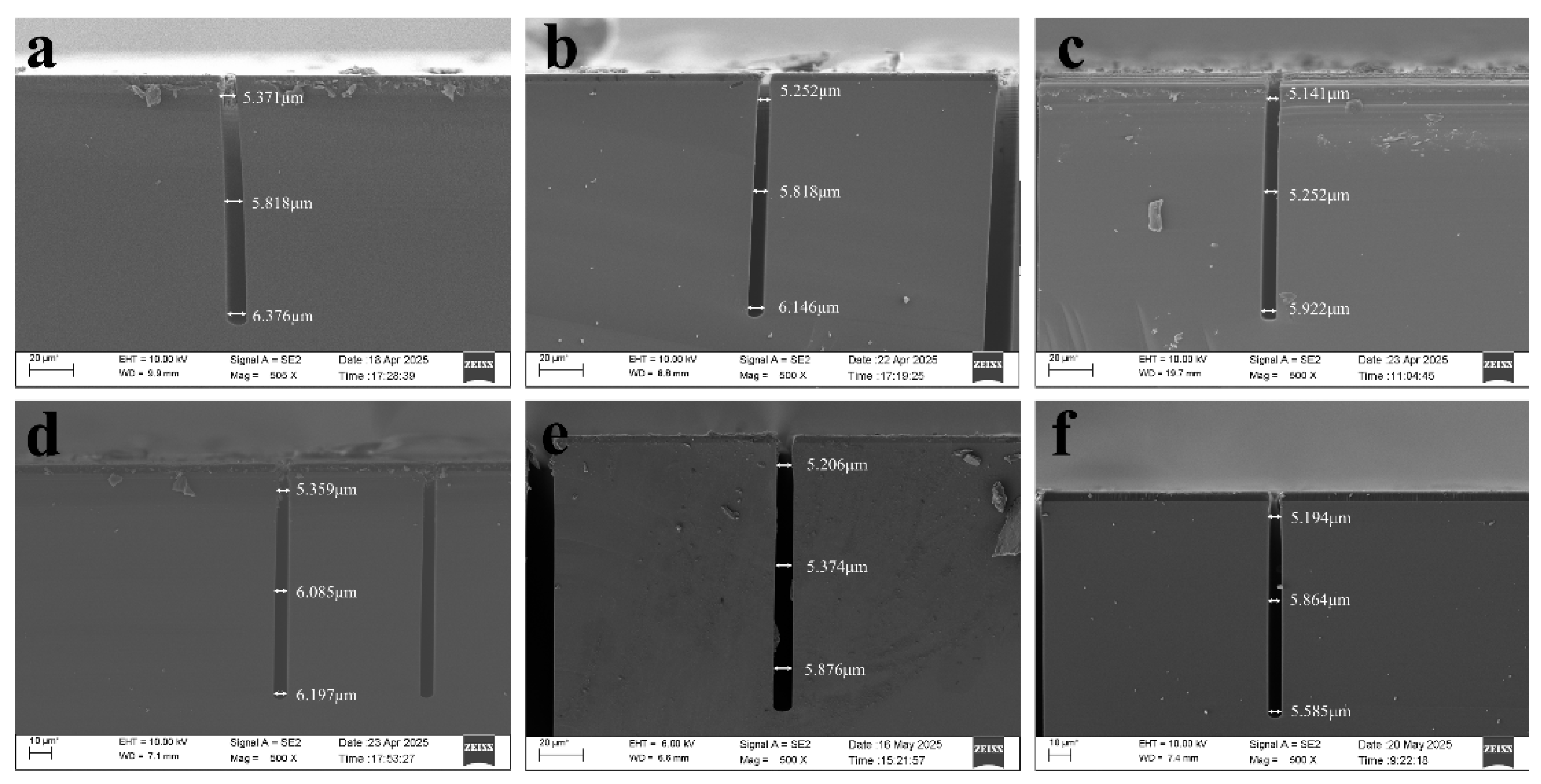
The bottom RF power increases with etch depth, meaning that as etching progresses downward, the bottom exhibits greater ion attraction. When ions reach the bottom, sputtering occurs, compromising sidewall protection. During the third etching step, lateral etching occurs, leading to increased lateral etching as etching progresses—that is, the opening size increases with depth. Specifically, the opening dimensions at the top, middle, and bottom of the pattern exhibit variations, with a maximum difference of 1.005 μm (between top and bottom). To mitigate this dimensional variation, analysis indicated insufficient sidewall passivation as a potential cause. Consequently, the passivation gas exposure time was appropriately extended from 1.5 seconds to 1.7 seconds, reducing the maximum opening size difference to 0.894 μm.
Increasing the passivation gas exposure time yields a slight improvement in the opening size variation. To enhance sidewall passivation, one can either extend the passivation gas exposure time or increase the passivation gas flow rate. Both approaches enhance sidewall passivation to reduce opening size variation. Alternatively, decreasing etch time lowers etch ion concentration, thereby reducing consumption of sidewall passivation and improving opening size variation. To further minimize opening size variation, the edge passivation gas flow rate was increased from 0 sccm to 50 sccm. The etch time was reduced back to the original 3 seconds, resulting in a reduced opening size difference of 0.781 μm.
The improvements to the above formulation had little effect on dimensional variation. Further analysis revealed that since bottom RF power increases with etch depth, extending passivation time also increases with etch depth. An alternative approach involved further reducing etch gas time while diminishing the increase in bottom RF power with etch depth. This reduced ion traction, decreased sputtering energy upon bottom impact, and consequently minimized consumption of sidewall passivation. Based on this, two sets of experiments were conducted. One set extended the passivation gas introduction time from 1.7s to 1.9s as the number of etching cycles increased, reducing the aperture size difference to 0.838μm. The other group further reduced the etching gas time to 2.9 seconds and decreased the bottom RF power from 100-120 to 100-110, narrowing the aperture size difference to 0.67 μm.
Following the aforementioned formulation adjustments, the variation in aperture size difference remained insignificant. Therefore, the formulation underwent comprehensive modification: the passivation time was uniformly set to 1.8 seconds regardless of etch depth. Similarly, the second-step passivation time was fixed at 1.8 seconds irrespective of etch depth. This reduction in duration decreased ion concentration, lowered bombardment intensity, and minimized consumption of sidewall passivation. The third step's chemical etching time was adjusted to 2.5 seconds, lowering the ion concentration and reducing chemical etching. The bottom RF power was set to 100-110, with edge passivation gas flow at 50 sccm. The etching results showed an aperture size difference of 0.67 μm, exhibiting faster etching in the middle with smaller apertures at the top and bottom (bowing effect).
Figure 4.
SEM images of etching results. (a) and (b) show SEM results from the first experimental group; (c) shows SEM results from the second experimental group; (d) and (e) show SEM results from the third experimental group; (f) shows SEM results from the fourth experimental group.
Figure 4.
SEM images of etching results. (a) and (b) show SEM results from the first experimental group; (c) shows SEM results from the second experimental group; (d) and (e) show SEM results from the third experimental group; (f) shows SEM results from the fourth experimental group.
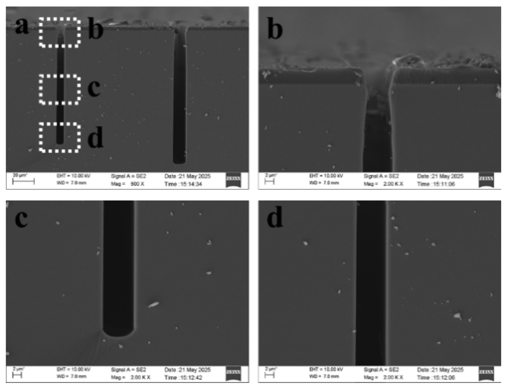
Sputtering on the sidewalls. This facilitates simple and convenient operation across various etch depths by eliminating variables that change with etch cycle count. Therefore, based on the aforementioned recipe, the bottom RF power was adjusted to 120W. The resulting etch aperture size variation was 0.279μm. The overall recipe contains no variables that change with each cycle count, and the aperture size variation also reached 0.279 μm.
Figure 5.
SEM images of etching results. (a) Overall etching morphology; (b) Top enlarged morphology; (c) Middle enlarged morphology; (d) Bottom enlarged morphology.
Figure 5.
SEM images of etching results. (a) Overall etching morphology; (b) Top enlarged morphology; (c) Middle enlarged morphology; (d) Bottom enlarged morphology.
Finally, a three-step Bosch process was employed to etch 4-inch silicon wafers using optimized parameters. The uniformity of bottom corner height differences and etch depth uniformity were measured at five points: top, center, bottom, left, and right. The measurement locations are shown in Figure 6. The measured etch depth and aperture size difference data for the five points are presented in Table 3. The etch depth uniformity was 3.09%. The uniformity formula is as follows:
4. Discussion
This study investigates the plasma etching process for 5μm-wide trench structures, with the core objective of enhancing the etch depth-to-width ratio while reducing the overall opening size variation (i.e., dimensional deviation between the top, middle, and bottom openings of the trench). It systematically summarizes the process optimization strategies to achieve this goal. The results demonstrate that precise control of key Bosch process parameters—including single-step deposition time, single-step etching time, and bottom RF power—significantly improves trench D/A ratio and effectively reduces overall opening size variation, successfully achieving the predetermined research objectives. The core mechanism of this process control strategy is as follows: Optimizing bottom RF power enhances the ion capture capability at the trench bottom. This alleviates the shortage of etchant supply at the bottom caused by gas replacement lag, addressing the critical bottleneck of “insufficient bottom etching drive” during DBR enhancement. Simultaneously, it reduces directional deviation during ion sputtering, minimizing non-uniform etching caused by ion reflection. Simultaneously, rational matching of single-step deposition time enables stable protective layer formation on trench sidewalls, preventing excessive sidewall etching. The synergistic effect of bottom RF power and single-step deposition time further suppresses expansion of aperture size deviation, ultimately achieving precise control over trench morphology.
The optimization scheme proposed in this study provides a critical theoretical foundation and directly implementable technical solution for developing plasma etching processes for “high-precision trench structures” in microelectromechanical system (MEMS) device manufacturing. It holds clear practical value and promising application prospects for advancing the manufacturing precision of core MEMS device structures, such as microfluidic channels and sensor electrode trenches.
Author Contributions
contributed to investigation, visualization, data curation, and writing—original draft: Dandan Wang. Conceptualization, Writing-review & editing, Supervision: Cheng Lei. Contributed to writing and editing: Pengfei Ji. Resources, Investigation: Zhiqiang Li. Investigation, Validation: Renzhi Yuan. Contributed to supervision and funding acquisition: Ting Liang, Contributed to supervision: Jiangang Yu, Contributed to supervision: Zong Yao, Contributed to supervision: Jialong Li.
Funding
This work is supported by the National Key Research and Development Program of China (No.2023YFB3209100).
Data Availability Statement
The original contributions presented in this study are included in the article. Further inquiries can be directed to the corresponding author.
Conflicts of Interest
The authors declare no conflicts of interest.
References
- Park J S, Kang D-H, Kwak S M, et al. Low-temperature smoothing method of scalloped DRIE trench by post-dry etching process based on SF6 plasma[J]. Micro and Nano Systems Letters, 2020, 8(1): 1–8.
- Cho D, Hong S, Lee M, et al. A review of silicon microfabricated ion traps for quantum information processing[J]. Micro and Nano Systems Letters, 2015, 3(1): 1-12. [CrossRef]
- Zhu F, Zhang X, Zhang H. Formation mechanism of multi-functional black silicon based on optimized deep reactive ion etching technique with SF6/C4F8[J]. Science China Technological Sciences,2015,58(2):381-389. [CrossRef]
- Kim T, Lee J. Optimization of deep reactive ion etching for microscale silicon hole arrays with high aspect ratio[J]. Micro and Nano Systems Letters, 2022, 10(1). [CrossRef]
- Wu B, Yi R, Ding X, et al. Surface evolution mechanism for atomic-scale smoothing of Si via atmospheric pressure plasma etching[J]. Journal of Manufacturing Processes,2024,132353-132362. [CrossRef]
- Chen H, Zhu C, Lin G, et al. Deep silicon etching technology and applications: a review[J]. Journal of Micromechanics and Microengineering, 2025, 35(8):083001. [CrossRef]
- Gao F, Sami Y, Markku K, et al. Smooth silicon sidewall etching for waveguide structures using a modified Bosch process[J]. Journal of Micro/Nanolithography, MEMS, and MOEMS, 2014, 13(1): 013010.
- Sygaya T, Yoon D. H, Yamazaki H et al. Simple and Rapid Fabrication Process of Porous Silicon Surface Using Inductively Coupled Plasma Reactive Ion Etching[J]. Journal of Microelectromechanical Systems, 2020, 29(1): 62-6.
- Golishnikov A A, Dyuzhev A N, Paramonov V V, et al. Research and Development of a Deep Anisotropic Silicon Plasma Etching Process with Reduced Sidewall Roughness of the Structures[J]. RussianMicroelectronics,2025,53(7):676-681. [CrossRef]
- Li Y, Yu L, Zhang Y, et al. Sub-200-nm-diameter cylindrical silicon nanopillars with high aspect ratio (40:1) fabricated by SF6/C4F8-modulated ICP-RIE[J]. Materials Science in Semiconductor Processing,2025,198109817. [CrossRef]
- Lakrathok A, Supadech J, Leepattarapongpan C, et al. Design of the comb-drive structure to reduce asymmetry lateral plasma etching on the cavity SOI substrate for MEMS fabrication[J]. Journal of Physics: Conference Series,2025,2934(1):012027-012027.
- Leyi Z, Zhihong G, Yongzhi F, et al. Research on the difference in etching rates of SiO2 at the top and bottom of a high-aspect-ratio trench in C4F8/Ar/O2 plasma etching[J]. Journal of Vacuum Science& Technology A, 2025, 43(3): 033003.
- Shi Z, Jefimovs K, Romano L, et al. Towards the Fabrication of High-Aspect-Ratio Silicon Gratings by Deep Reactive Ion Etching[J]. Micromachines, 2020, 11(9): 864. [CrossRef]
- Tang Y, Saandoughsa A, OWEN K J, et al. Ultra Deep Reactive Ion Etching of High Aspect-Ratio and Thick Silicon Using a Ramped-Parameter Process[J]. Journal of Microelectromechanical Systems, 2018, 27(4): 686-697.
- Haoming G, Shengbin C, Lei L, et al. A review on the mainstream through-silicon via etching methods[J]. Materials Science in Semiconductor Processing,2022,137.
- Barrantes A A J, Mastrangeli M, Thoen J D, et al.Superconducting High-Aspect Ratio Through-Silicon Vias with DC-Sputtered Al for Quantum 3D integration[J]. IEEE Electron Device Letters,2020, (99):1. [CrossRef]
- Gao Z, Ma Z, Gao L, et al. Etching mechanism of high-aspect-ratio array structure[J]. Microelectronic Engineering,2023,279.
- J.A. A, M. M, D.J. T, et al. Fabrication of Al-Based Superconducting High-Aspect Ratio TSVS for Quantum 3D Integration[J].Proceedings of the IEEE International Conference on Micro Electro Mechanical Systems (MEMS), 2020:932-935.
- Ni Z-H, Xia Y, Hu C F, et al. Metallization filling and electrical performance of high-aspect-ratio through silicon via with electroless deposited Co liner[J]. ECS Journal of Solid State Science and Technology, 2025, 14(5): 054003. [CrossRef]
- Zhang D, Smith D, Kumarapuram G, et al. Process development and optimization for 3 μm high aspect ratio via-middle through-silicon vias at wafer level[J]. IEEE Transactions on Semiconductor Manufacturing, 2015, 28(4): 454–460. [CrossRef]
- Aixi P, Medhat, Zheng, et al. Fabrication of ultrahigh aspect ratio Si nanopillar and nanocone arrays[J]. Journal of Vacuum Science& Technology B, 2023, 41(2): 023001.
- Nonaka T, Takahashi K, Uchida A, et al. Morphology of films deposited on the sidewall during the Bosch process using C4F8 plasmas[J]. Journal of Micromechanics and Microengineering,2024,34(8):085014.
- Tomoyuki Nonaka, Kazuo Takahashi, Akimi Uchida, et al. Effects of C4F8 plasma polymerization film on etching profiles in the Bosch process[J]. Journal of Vacuum Science& Technology A, 2023, 41(6): 063004. [CrossRef]
- BatesL R, Thamban SL P, GoecknerJ M, et al. Silicon etch using SF6/C4F8/Ar gas mixtures[J]. Journal of Vacuum Science & Technology A: Vacuum, Surfaces, and Films,2014,32(4):041302.
- Jack Nos, Sylvain Iséni, Martin Kogelschatz, et al. Cryogenic cyclical etching of Si using CF4 plasma passivation steps: The role of CF radicals[J]. Applied Physics Letters, 2025, 126(3): 031602. [CrossRef]
Figure 1.
(a) Mask pattern: 5-25 × 5000 μm, with 100 μm spacing between patterns and 200 μm array pitch. (b) Scanning electron microscope image of the standard process.
Figure 1.
(a) Mask pattern: 5-25 × 5000 μm, with 100 μm spacing between patterns and 200 μm array pitch. (b) Scanning electron microscope image of the standard process.
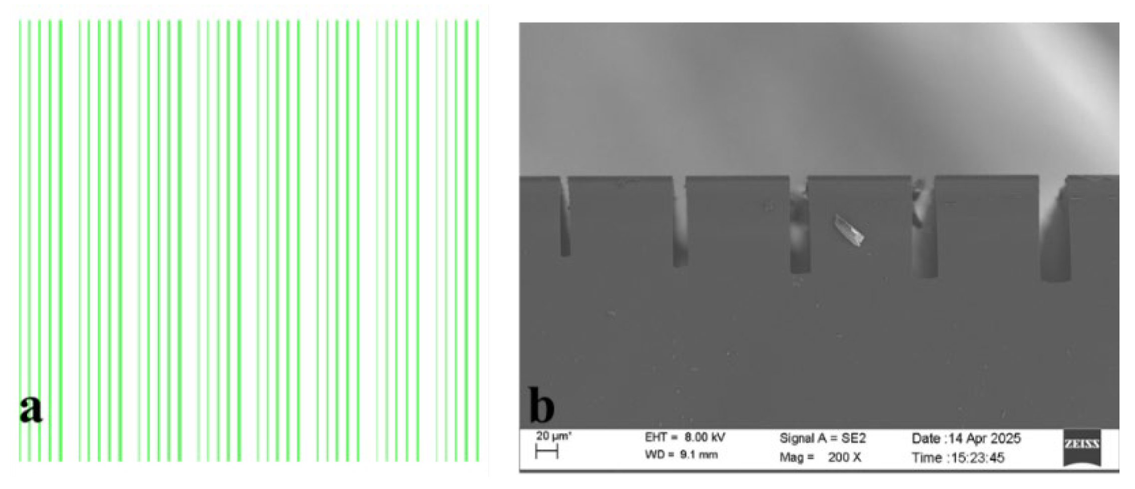
Figure 6.
4-inch wafer test position.
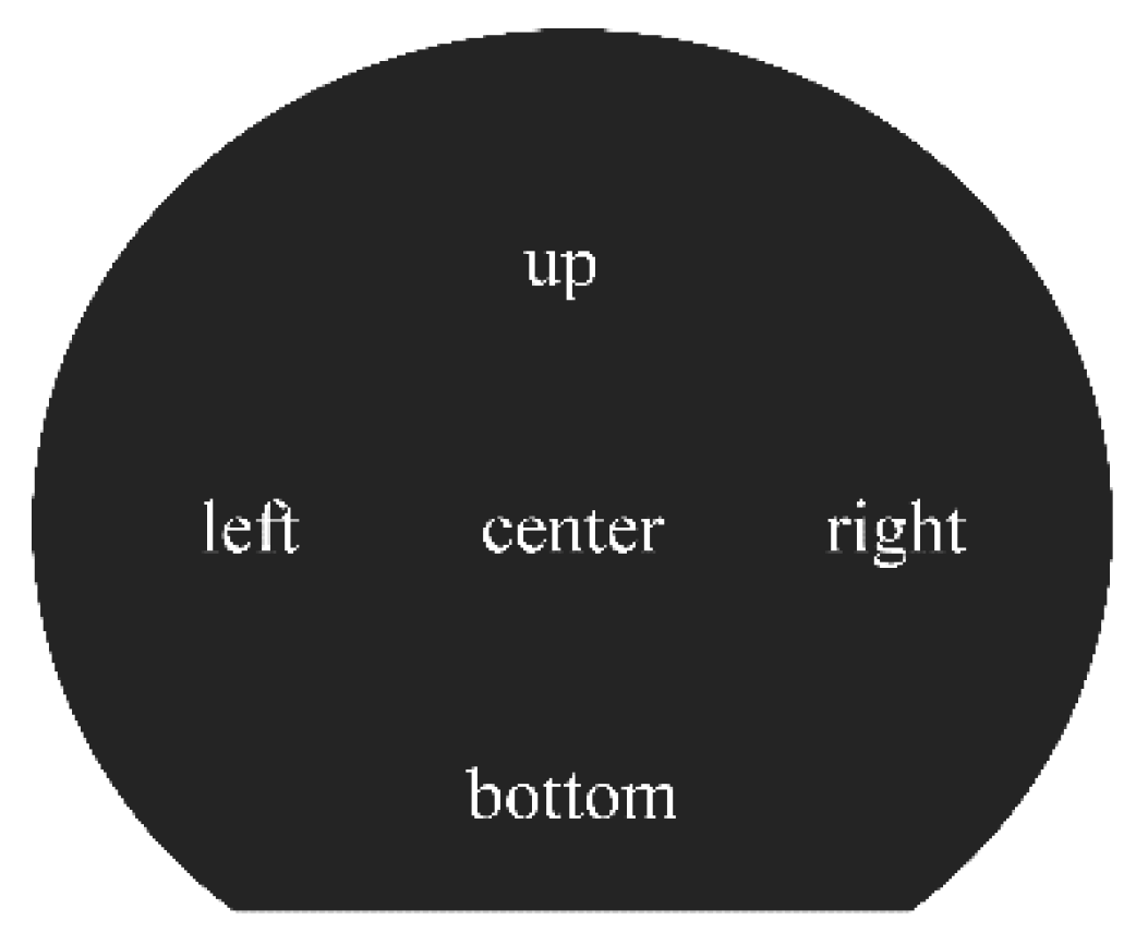

Table 1.
Basic Formulation.
| Parameters | Cycles | Time/s | center C4F8/sccm | edge C4F8/sccm | center SF6/sccm | edge SF6/sccm | LFPower/W |
|---|---|---|---|---|---|---|---|
| Dep | 100 | 1.5 | 180 | 0 | 0 | 0 | 10 |
| Etch1 | 100 | 2 | 0 | 0 | 300 | 300 | 100 |
| Etch2 | 100 | 3 | 0 | 0 | 300 | 300 | 40 |
Table 2.
Etching Parameter Experiments.
| Parameters | Cycles | Time(sec) | center C4F8/sccm | edge C4F8/sccm | LFPower | |
|---|---|---|---|---|---|---|
| A | Dep | 100→150→180 | 1.5 | 180 | 0 | 10 |
| Etch1 | 2 | 0 | 0 | 100 | ||
| Etch2 | 3 | 0 | 0 | 40 | ||
| B | Dep | 180 | 1.5/1.5→1.7 | 180 | 0 | 10 |
| Etch1 | 2 | 0 | 0 | 100-120/100-110 | ||
| Etch2 | 3-3.5/3-3.2 | 0 | 0 | 40 | ||
| C | Dep | 180 | 1.7/1.7-1.9 | 180 | 50 | 10 |
| Etch1 | 2 | 0 | 0 | 100-110→100-120 | ||
| Etch2 | 2.9→3 | 0 | 0 | 40 | ||
| D | Dep | 200 | 1.8 | 180 | 50 | 10 |
| Etch1 | 1.8 | 0 | 0 | 100-100→120 | ||
| Etch2 | 2.5 | 0 | 0 | 40 |
Table 3.
Etching Results Data.
| Position | Etch Depth/μm | Opening Size Difference/μm |
|---|---|---|
| center | 106.662 | 0.279 |
| up | 106.1 | 0.279 |
| bottom | 108.3 | 0.335 |
| left | 109.427 | 0.340 |
| right | 108.3 | 0.340 |
Disclaimer/Publisher’s Note: The statements, opinions and data contained in all publications are solely those of the individual author(s) and contributor(s) and not of MDPI and/or the editor(s). MDPI and/or the editor(s) disclaim responsibility for any injury to people or property resulting from any ideas, methods, instructions or products referred to in the content. |
© 2025 by the authors. Licensee MDPI, Basel, Switzerland. This article is an open access article distributed under the terms and conditions of the Creative Commons Attribution (CC BY) license (http://creativecommons.org/licenses/by/4.0/).
Copyright: This open access article is published under a Creative Commons CC BY 4.0 license, which permit the free download, distribution, and reuse, provided that the author and preprint are cited in any reuse.


