1. Introduction
Lead telluride (PbTe), a semiconductor with a narrow band gap (0.22 eV and 0.32 eV at 60 K and 300 K, respectively [
1]), exhibits high photosensitivity in the mid-infrared spectral region. The type of conductivity and carrier concentration in PbTe are determined by deviation from stoichiometry and can be adjusted by growth conditions or post-growth treatment enabling the fabrication of p-n diodes. Due to the narrow band gap, p-n diodes made of PbTe must be cooled to cryogenic temperatures to maintain their rectifying properties and infrared sensitivity, what limits applications of this material [
2,
3]. Cadmium telluride (CdTe), an II-VI semiconductor with a wide energy gap, is known for its excellent optical properties in the visible spectral range, making the material useful for light detectors and highly efficient solar cells [
4,
5,
6,
7]. These excellent optical properties include a very high absorption coefficient of 106 cm-1 and an direct energy gap well matched to the maximum of the solar spectrum of 1.49 eV at room temperature. Since CdTe can be doped to both n-type or p-type, it is relatively easy to make p-n diodes based on CdTe. In order to increase the hole concentration, p-type CdTe is often replaced with acceptor doped Zn-containing layers such as p-type CdZnTe or ZnTe. In recent years, properties of p-n diodes made of CdTe and related materials such as CdTe, CdMgTe, CdMnTe, CdZnTe and ZnTe have been studied by various experimental methods [
8,
9,
10,
11].
Structures made from a combination of CdTe and PbTe are easy to grow by epitaxial methods, such as molecular beam epitaxy (MBE), because the both constituents are cubic semiconductors with very close lattice parameters i.e., 0.6462 nm for PbTe and 0.648 nm for CdTe [
12] and thus the lattice mismatch is very low, of about 0.3%. However, PbTe crystallizes in a rock salt structure while CdTe in a zinc blende structure. Difference in the crystal structures of both semiconductors has important consequences: (1) PbTe and CdTe are nearly immiscible, forming areas of pure PbTe and CdTe with well-defined interfaces, and (2) there are a large number of dangling bonds at the PbTe/CdTe interfaces that can capture free carriers from adjacent PbTe regions. The immiscibility effect was used to produce PbTe quantum dots of ideal shape in a CdTe matrix exhibiting strong infrared photo- and electroluminescence [
13,
14,
15,
16]. The reverse case, i.e., CdTe quantum dots embedded in a PbTe matrix, was studied using transport measurements to investigate the effect of the antidots on the thermoelectricity of PbTe films [
17,
18]. Photoresistors made of PbTe/CdTe multilayers exhibit strong photosensitivity to infrared radiation up to the room temperature and can be used as high temperature infrared detectors [
19,
20,
21,
22].
The aim of this study is to extend the previous investigation of p-ZnTe/n-CdTe diodes with PbTe nano-inclusions incorporated within their charge depletion region [
23]. The novelty of this work lies in the use of PbTe nano-inclusions in the form of zero-dimensional quantum dots (QDs), in contrast to our previous study, which focused on the influence of two-dimensional PbTe layers or multilayers on the performance and characteristics of wide-bandgap p-ZnTe/n-CdTe diodes. Our results demonstrate that the incorporation of PbTe QDs significantly broadens the optical sensitivity of wide-bandgap diodes, extending it into the mid-infrared region. Importantly, this enhanced infrared sensitivity persists at room temperature, highlighting the potential of these devices for applications in two-color high-temperature detectors and solar cells.
2. Materials and Methods
The overall design of the studied diodes and their fabrication procedure are very similar to those reported in our previous publication [
23]. As before, the p-ZnTe/n-CdTe diodes containing PbTe quantum dots (QDs) were grown by molecular beam epitaxy (MBE) on semi-insulating GaAs (100) substrates using elemental effusion cells containing ultra-pure (7N) Cd, Zn, Pb, and Te. In the first stage, a p-type ZnTe buffer layer was deposited. The ZnTe layer, with a thickness of 2.8 µm, was doped with nitrogen acceptors supplied by a radio-frequency nitrogen plasma source. In the second stage, the depleted charge region of the diode was formed by the growth of an undoped PbTe/CdTe multilayer structure. This structure consisted of 20 repetitions of 13 nm thick PbTe layers separated by 21 nm thick CdTe barriers. To transform the thin PbTe layers into rows of quantum dots, the structure was annealed for 10 minutes at the growth temperature of 350 °C, as described in Refs. [
13,
14,
15,
16]. In the final step of the MBE process, the structure was covered with a 0.37 µm thick n-type CdTe layer. To achieve n-type conductivity, this layer was doped with iodine donors supplied from a solid ZnI
2 source. The estimated carrier concentrations in the n-type and p-type layers were 1–3 × 10
19 cm
−3. To expose the internal p-type ZnTe layer for electrical contact, a mesa structure was etched using a methanol–bromine solution. Electrical contacts were then formed on both sides of the diodes by indium soldering.
Cross-sectional imaging of the diodes structure and electron beam-induced current (EBIC) measurements of the p-ZnTe/n-CdTe diodes with PbTe QDs were carried out in a scanning electron microscope (SEM) ZEISS EVO HD15 SEM using a Digital Image Scanning System 5 EBIC system in the microscope chamber. An accelerating voltage of 20 kV and a 500 pA beam current were used. The EBIC signals were measured at temperatures range from 80 K to 300K. SEM imaging was used to visualize the overall structure of the p-ZnTe/n-CdTe diodes with PbTe quantum dots and to determine the actual thickness of individual layers. For that the structures were cleaved along the growth direction, i.e., the [100] axis, and scans were taken in the (011) planes, which are the easy-cleavage planes of zinc-blende II–VI crystals.
3. Results and Discussion
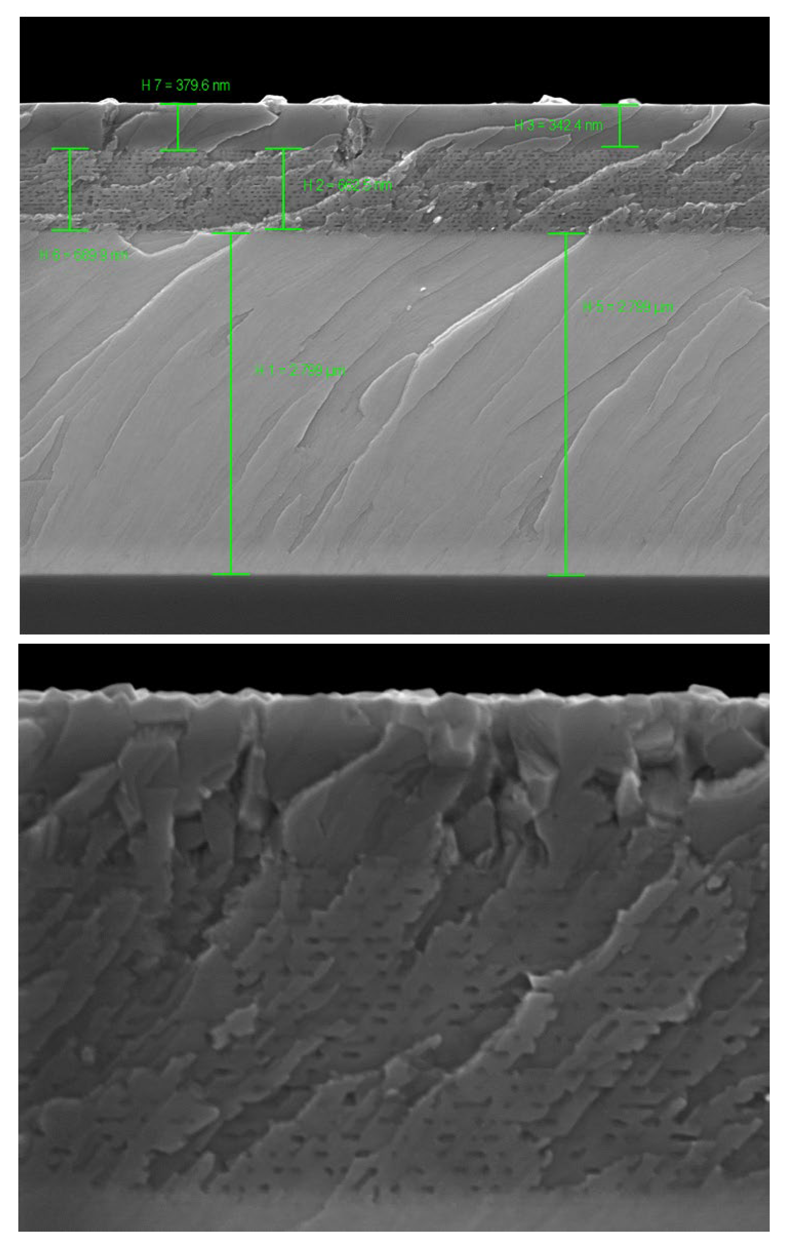
The upper panel of
Figure 1 depicts a cross-sectional SEM image of the diode, highlighting its layered structure. Horizontal stripes of varying contrast clearly delineate the GaAs substrate, the p-type ZnTe layer, the PbTe/CdTe multilayer region, and the n-type CdTe cap. The layer thicknesses determined from the SEM image—2.8, 0.68, and 0.37 µm, respectively—are in good agreement with the values expected from the MBE growth parameters. The lower panel of
Figure 1 shows the PbTe/CdTe multilayer region at higher magnification. Rows of PbTe QDs separated by CdTe barriers are distinctly visible. The average dimensions of the QDs are approximately 16-18 nm in height and 25-35 nm in length, with adjacent QDs rows spaced by about 21 nm.
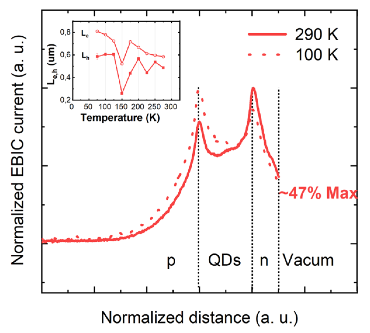
The electron beam current induced (EBIC) scan across the structure is shown in
Figure 2. The maximum of the EBIC signal occurs at the point where the embedded electric field is strongest, indicating the location of the p–n junction. In the case our diodes a double peak appears what indicates that the layer containing PbTe QDs is quasi-insulating and thus it forms two p-n junctions with both the p-type and n-type layers of the structure. The inset of
Figure 2 shows the minority carrier diffusion lengths (Le,h) for electrons and holes extracted from EBIC scans according to the following relation: IEBIC=I0 exp(-x/ Le,h), where IEBIC is the EBIC signal, I0 is a constant, x describes the position of the generating electron beam [
24,
25]. The diffusion lengths obtained from the EBIC scans are relatively short (Le=0.7–0.8 μm, Lh=0.5–0.6 μm) and show only a weak dependence on temperature. Short diffusion lengths were also observed in our previous study [
23]. To enhance the collection of photoexcited carriers at the metallic contacts—and thus improve the light sensitivity of the diodes—the n-type cap layer was made significantly thinner (0.38 µm) compared to the previous study (0.92 µm). As a result of the thinner cap, the electron beam–induced current at the metallic contact reaches 47% of its maximum value, compared to only a few percent for the thicker cap.
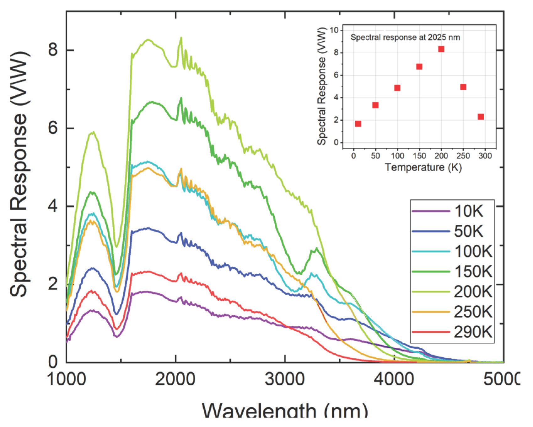
The typical photosensitivity spectra of the p-ZnTe/n-CdTe diode with integrated PbTe QDs, measured in the infrared (IR) spectral region at temperatures from 10 to 290 K, are shown in
Figure 3. The measurements were performed using an infrared spectrometer consisting of an M150 monochromator (Solar Laser System), a Nernst lamp as the infrared light source, and a Thorlabs mechanical chopper operating at a modulation frequency of 730 Hz. The output signal was detected using a Zurich Instruments MFLI 500 kHz / 5 MHz
Lock-in Amplifier. During optical measurements illumination was applied through the n-type CdTe cap layer. The diodes exhibit a pronounced photo-response to infrared radiation, persisting up to room temperature. As shown in the inset to
Figure 3, the photosensitivity increases significantly with decreasing temperature, reaching a maximum at T = 200 K. A further decrease in temperature results in a reduction of the signal intensity. The maximum sensitivity, observed at a wavelength of 2.0 µm and 200 K, attains a value of 8 V/W.
Notably, the sensitivity of the diodes incorporating QDs increased by nearly an order of magnitude compared to closely related devices containing single- or multi-layer PbTe nano-inclusions, as reported in our previous work [
23]. This enhancement is likely associated with two main factors. First, in QD-based diodes, a substantial fraction of the electrons traversing the p–n junction can bypass the PbTe nano-inclusions and transition from the p-type to the n-type region through the intrinsic CdTe layer. This transport pathway is unavailable in structures where PbTe nano-inclusions form single or multiple layers oriented perpendicular to the electron flow. In those configurations, electrons become trapped in the potential wells of the PbTe layers, and their subsequent transport requires tunneling across the PbTe–CdTe interfaces. Second, as mentioned above, the increased photosensitivity can be attributed to the thinner n-type cap layer. Owing to this reduced thickness, a greater proportion of photoexcited electrons can successfully reach the surface contact of the diode (see
Figure 2).
The temperature affects not only the intensity of the photo-response, but also the shape of the spectrum, especially in the long wavelength region. While at 290 K the signal fades at about 3.8 μm, at 10 K the IR response of the signal is observed up to about 4.5 μm. The cut-off energies increase linearly with increasing temperature indicating that the sensitivity of broadband p-ZnTe/n-CdTe diodes in the mid-infrared spectral region is due to the presence of PbTe QDots. The observed blue shift of the measured cut-off energies, relative to the PbTe energy gap is most likely due to a quantum confinement effect.
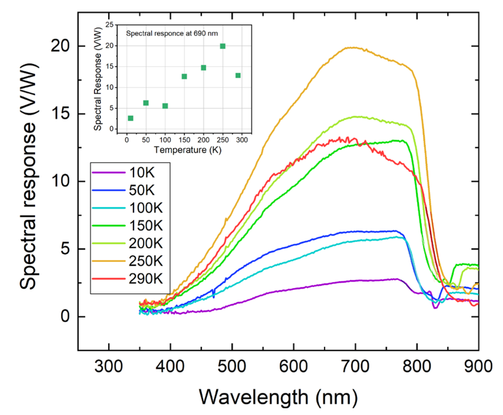
The diodes also exhibit sensitivity to radiation in the visible spectral region, as shown in
Figure 4. In this region, the photoresponsivity signal is stronger than in IR, reaching 20 V/W at a wavelength of approximately 0.7 µm and at a slightly higher temperature of 250 K.
Considering the lock-in amplifier load resistance of 1 MΩ, the zero-bias resistance of the diode of approximately 10 kΩ, and the diode active area of 1.16 mm2, the estimated detectivities of the device are relatively low both in the infrared and visible spectral ranges, amounting to 7 × 107 cm·Hz1/2/W and to 2 × 108 cm·Hz1/2/W, respectively. Although the detectivity values are lower than those of optimized infrared and visible light detectors, the p-ZnTe/n-CdTe diodes with integrated PbTe QDs demonstrate a broad spectral response—from the visible to the mid-infrared region—while maintaining operation at room temperature. These characteristics make the devices a promising candidate for broadband sensing and multispectral photodetection applications.
4. Summary
The presented studies show that the introduction of narrow-band PbTe QDs into the depletion region of wide bandgap II-VI semiconductors (p-ZnTe/n-CdTe) diodes makes them sensitive to infrared radiation without destroying their overall performance. The diodes remain photosensitive up to the room temperature. The minority carrier diffusion lengths estimated from EBIC measurements are relatively short, what suggests that better responsivity can be obtained by decreasing the distance between the depletion layer and the electrical contacts. The results prove that this kind of devices may be attractive candidates for high temperature infrared detectors and dual-color solar cells.
Author Contributions
Conceptualization, G.K.; methodology, M.Sz. and J.M.G.; validation, G.K.; investigation, J.M.G.; writing—original draft preparation, G.K.; writing—review and editing, G.K. and M.Sz and J.M.G. All authors have read and agreed to the published version of the manuscript.
Funding
This research was funded by National Science Center (Poland), grant number 2012/41/B/ST3/03651.
Conflicts of Interest
The authors declare no conflicts of interest
References
- Bilc, D. I.; Mahanti, S. D.; Kanatzidis, M. G. Electronic transport properties of PbTe and AgPbmSbTe2+m
systems. Phys. Rev. B 2006, 74, 125202.
- Rogalski, A. Infrared and Terahertz Detectors; CRC Press: Boca Raton, FL, USA, 2019.
- Rogalski, A. Infrared Detectors, 2nd ed.; CRC Press: Boca Raton, FL, USA, 2001.
- Britt, J.; Ferekides, C. Thin-film CdS/CdTe solar cell with 15.8% efficiency. Appl. Phys. Lett. 1993, 62, 2851–2853.
- Shkir, M.; Khan, M. T.; Ashraf, I. M.; Almohammedi, A.; Dieguez, E.; AlFaify, S. High-performance visible-light photodetectors based on inorganic CZT and InCZT single crystals. Sci. Rep. 2019, 9, 12436.
- Wu, X. High-efficiency polycrystalline CdTe thin-film solar cells. Sol. Energy 2004, 77, 803–814.
- Valmik, B. G.; Deshpande, M. P.; Bhatt, S. V.; Sathe, V.; Bhoi, H. R.; Rajput, P.; Chaki, S. H. Investigation and fabrication of cadmium telluride (CdTe) single crystal as a photodetector. Physica B 2021, 614, 413027.
- Wichrowska, K.; Wosiński, T.; Domagała, J. Z.; Kret, S.; Chusnutdinow, S.; Karczewski, G. Structural defects in MBE-grown CdTe-based heterojunctions designed for photovoltaic applications. Semicond. Sci. Technol. 2021, 36, 045022.
- Yahia, I. S.; AlFaify, S.; Abutalib, M. M.; Chusnutdinow, S.; Wojtowicz, T.; Karczewski, G.; Yakuphanoglu, F.; Al-Bassam, A.; El-Naggar, A. M.; El-Bashir, S. M. n-(CdMgTe/CdTe)/(p-(CdTe/ZnCdTe/ZnTe)/p-GaAs) heterostructure diode for photosensor applications. Appl. Phys. A 2016, 122, 491.
- Yahia, I. S.; Yakuphanoglu, F.; Chusnutdinow, S.; Wojtowicz, T.; Karczewski, G. Photovoltaic characterization of n-CdTe/p-CdMnTe/GaAs diluted magnetic diode. Curr. Appl. Phys. 2013, 13, 537–542.
- Yahia, I. S.; Sakr, G. B.; Wojtowicz, T.; Karczewski, G. p-ZnTe/n-CdMnTe/n-GaAs diluted magnetic diode for photovoltaic applications. Semicond. Sci. Technol. 2010, 25, 095001.
- Karczewski, G.; Szot, M.; Kret, S.; Kowalczyk, L.; Chusnutdinow, S.; Wojtowicz, T.; Schreyeck, S.; Brunner, K.; Schumacher, C.; Molenkamp, L. W. Nanoscale morphology of multilayer PbTe/CdTe heterostructures and its effect on photoluminescence properties. Nanotechnology 2015, 26, 135601.
- Heiss, W.; Groiss, H.; Kaufmann, E.; Hesser, G.; Böberl, M.; Springholz, G.; Schäffler, F.; Koike, K.; Harada, H.; Yano, M. Centrosymmetric PbTe/CdTe quantum dots coherently embedded by epitaxial precipitation. Appl. Phys. Lett. 2006, 88, 192109.
- Koike, K.; Harada, H.; Itakura, T.; Yano, M.; Heiss, W.; Groiss, H.; Kaufmann, E.; Hesser, G.; Schäffler, F. Photoluminescence characterization of PbTe/CdTe quantum dots grown by lattice-type mismatched epitaxy. J. Cryst. Growth 2007, 301, 722–728.
- Schwarzl, T.; Kaufmann, E.; Springholz, G.; Koike, K.; Hotei, T.; Yano, M.; Heiss, W. Temperature-dependent midinfrared photoluminescence of epitaxial PbTe/CdTe quantum dots and calculation of the corresponding transition energy. Phys. Rev. B 2008, 78, 165320.
- Hochreiner, A.; Schwarzl, T.; Eibelhuber, M.; Heiss, W.; Springholz, G.; Kolkovsky, V.; Karczewski, G.; Wojtowicz, T. Midinfrared electroluminescence from PbTe/CdTe quantum dot light-emitting diodes. Appl. Phys. Lett. 2011, 98, 021106.
- Szot, M.; Dybko, K.; Dziawa, P.; Kowalczyk, L.; Smajek, E.; Domukhovski, V.; Taliashvili, B.; Dłużewski, P.; Reszka, A.; Kowalski, B. J.; Wiater, M.; Wojtowicz, T.; Story, T. Epitaxial Zinc-Blende CdTe Antidots in Rock-Salt PbTe Semiconductor Thermoelectric Matrix. Cryst. Growth Des. 2011, 11, 4794–4802.
- Szot, M.; Dybko, K.; Dziawa, P.; Kowalczyk, L.; Domukhovski, V.; Taliashvili, B.; Reszka, A.; Kowalski, B.; Dłużewski, P.; Wiater, M.; Wojtowicz, T.; Story, T. Electric and thermoelectric properties of CdTe/PbTe epitaxial nanocomposite. Func. Mater. Lett. 2014, 7, 1440007.
- Chusnutdinow, S.; Schreyeck, S.; Kret, S.; Kazakov, A.; Karczewski, G. Room temperature infrared detectors made of PbTe/CdTe multilayer composite. Appl. Phys. Lett. 2020, 117, 072102.
- Chusnutdinow, S.; Kazakov, A.; Jakieła, R.; Szot, M.; Schreyeck, S.; Brunner, K.; Karczewski, G. Effect of manganese alloying on infrared detectors made of Pb1-xMnxTe/CdTe multilayer composite. Materials 2023, 16, 4211.
- Zhu, J. Q.; Xu, H. L.; Ma, S. S.; Wang, Z. L.; Li, K.; Ali, N. S. R.; Zhong, J.; Zhou, Q. H.; Lai, W. E.; Wu, H. Z. Ultrahigh-speed mid-infrared photodetectors with 2-D electron gas in a CdTe/PbTe heterojunction. IEEE Trans. Electron Devices 2020, 67, 2432–2438.
- Zhu, J. Q.; Xu, H. L.; Wang, Z. L.; Chen, Y. S.; Ma, S. S.; Ali, N.; Zhu, H. M.; Rahimi-Iman, A.; Wu, H. Z. Lateral photovoltaic mid-infrared detector with a two-dimensional electron gas at the heterojunction interface. Optica 2020, 7, 1394–1401.
- Głuch, J. M.; Szot, M.; Chusnutdinow, S.; Karczewski, G. Wide gap II–VI diodes with PbTe nano-inclusions for infrared detection and photovoltaics. Appl. Phys. Lett. 2025, 126, 121101.
- Przeździecka, E.; Stachowicz, M.; Chusnutdinow, S.; Jakieła, R.; Kozanecki, A. Electron beam induced current profiling of the p-ZnO:N/n-GaN heterojunction. Appl. Phys. Lett. 2015, 106, 062106.
- Bandić, Z. Z.; Bridger, P. M.; Piquette, E. C.; McGill, T. C. Minority carrier diffusion length and lifetime in GaN. Appl. Phys. Lett. 1998, 72, 3166–3168.
|
Disclaimer/Publisher’s Note: The statements, opinions and data contained in all publications are solely those of the individual author(s) and contributor(s) and not of MDPI and/or the editor(s). MDPI and/or the editor(s) disclaim responsibility for any injury to people or property resulting from any ideas, methods, instructions or products referred to in the content. |
© 2025 by the authors. Licensee MDPI, Basel, Switzerland. This article is an open access article distributed under the terms and conditions of the Creative Commons Attribution (CC BY) license (http://creativecommons.org/licenses/by/4.0/).