
Submitted:
12 June 2024
Posted:
12 June 2024
You are already at the latest version
Abstract
Materials engineering based on metal oxides for manipulating the solar spectrum and producing solar energy have been under intense investigation over the last years. In this work, we present NiO thin films double-doped with niobium (Nb) and nitrogen (N) as cation and anion dopants (NiO:(Nb,N)) to be used as p-type layers in all oxide transparent solar cells. The films were grown by sputtering a composite Ni-Nb target on room-temperature substrates in plasma containing 50% Ar, 25% O2 and 25% N2 gases. The existence of Nb and N dopants in the NiO structure was confirmed by the Energy Dispersive X-Ray and X-Ray Photoelectron Spectroscopy techniques. The nominally undoped NiO film, which was deposited by sputtering a Ni target and used as the reference film, was oxygen-rich, single-phase cubic NiO, having a visible transmittance of less than 20%. Upon double doping with Nb and N the visible transmittance of NiO:(Nb,N) film increased to 60%, which was further improved after thermal treatment to around 85%. The respective values of the direct band gap in the undoped and double-doped films were 3.28 eV and 3.73 eV just after deposition and 3.67 eV and 3.76 eV after thermal treatment. The changes in the properties of the films such as structural disorder, direct and indirect energy band gaps, Urbach tail states and resistivity were correlated with the incorporation of Nb and N in their structure. The thermally treated NiO:(Nb,N) film was used to form a diode with a spin-coated two-layer, mesoporous on top of a compact, TiO2 film. The NiO:(Nb,N)/TiO2 heterojunction exhibited visible transparency of around 80%, showed rectifying characteristics and the diode’s parameters were deduced using the I-V method. The diode revealed photovoltaic behavior upon illumination with UV light exhibiting a short circuit current density of 0.2 mA/cm2 and open-circuit voltage of 500 mV. Improvements of the output characteristics of the NiO:(Nb,N)/TiO2 UV-photovoltaic by proper engineering of the individual layers and device processing procedures are addressed. Transparent NiO:(Nb,N) films can be potential candidates in all-oxide ultraviolet photovoltaics for tandem solar cells, smart windows and other optoelectronic devices.
Keywords:
NiO
; NiO co-doping
; NiO:(Nb
; N)
; TiO2
; ultraviolet photovoltaic
; NiO/TiO2 heterojunction
; Urbach tail
; sputtering
; mesoporous TiO2
; optical properties
1. Introduction
It has been realized that we are experiencing a climatic change. A complete decarbonization of the energy system towards a net-zero future has to be accelerated by employing a clean, renewable energy system for all energy end-use sectors: power, heating/cooling and transport, securing at the same time energy supplies. Thus, fundamental changes to the way energy is supplied, used, stored, transmitted, bought and sold, are necessary to satisfy energy, environmental and health issues. In addition, it is worth considering that the built environment accounts for more than 45% of the primary energy used in Europe and is responsible for 36% of greenhouse gases [1,2]. This huge amount of energy consumption is mainly due to heating, cooling and lighting in residential and commercial buildings, where humans spend almost 90% of their time. Future zero-energy buildings require user-controlled smart windows which can control glare, manage thermal/visual comfort and at the same time be capable of powering wearable and mobile health in-door sensing systems including circuits for the Internet of Things (IoT) [3]. Such energy producing smart windows require the use of transparent solar cells utilizing the ultraviolet (UV) part of the solar spectrum. UV solar radiation accounts for around 7% of the solar spectrum while the theoretical efficiency of transparent photovoltaics (PV) has been estimated to be 21% [4]. Wide band gap oxide-based semiconductors, with high visible transmittance, can be used for forming the required p-n junction and thus fabricating transparent PVs absorbing the ultraviolet radiation.
Nickel oxide (NiO) is the most commonly used p-type oxide and, provided it can be sufficiently transparent, it has been used with transparent n-type oxides like In2O3:Sn (ITO), ZnO and TiO2 to form a p/n junction and realize solar-blind devices absorbing the ultraviolet solar radiation. All-oxide NiO-based ultraviolet photovoltaics (UV-PVs) have been reported for NiO/TiO2 [5,6,7,8,9] and NiO/ZnO [10,11,12,13,14]. As in the case of conventional PVs, the main factors determining the conversion efficiency are: (i) the efficient absorption of photons at the front illuminated surface and generation of carriers, (ii) the efficient separation and transfer of these photogenerated carriers across the device with the aid of the built-in electrostatic field at the interface and (iii) the collection of the photogenerated carriers at the respective electrodes. Three techniques are generally followed to achieve PV with lesser loss mechanisms and higher output characteristics. Firstly, the layers consisting of the PV device are generally deposited/formed on intentionally heated substrates or on unheated substrates followed by post-deposition heat treatments (≥ 300 oC) so as to create layers with less structural defects, stress and distortion, minimizing thus recombination centers/states for the photogenerated carriers. Secondly, suitable dopants are introduced which, as mentioned above, can reduce structural defects/vacancies, affect the electronic structure, defect levels and the properties of the layers. Thirdly, the insertion of an interlayer at the interface to spatially enhance the built-in electrostatic field and subsequently improve photocurrent and photovoltage [11,15]. For the case of NiO/TiO2 UV-PVs, improvements in the performance of the devices have been achieved by following some of the above mentioned techniques. For example, heat treatments up to 600oC have been employed [9,11], dopants like N in TiO2 [6] or Nb in NiO [7] have been used or suitable interlayers have been inserted at the NiO-TiO2 interface like SnS or MgO [16,17] so to enhance the output characteristics of the UV-PVs.
In a previous investigation we have shown that nitrogen doping in NiO can improve its transparency by minimizing structural disorder, energy band gap widening [18] and reduction of mid-band-gap states [19]. In addition, it was revealed that p-type Nb-doped NiO can exhibit photovoltaic behaviour when forming a p/n junction with mesoporous TiO2 [7]. In this work, we proceeded in a combinatorial and selective double doping of NiO in an attempt to enhance further the photovoltaic output characteristics of the transparent NiO/TiO2 heterostructure. The rf-sputtered NiO layer was co-doped with the optimum amounts of anion (nitrogen -N) and cation (niobium -Nb) dopants. The fabricated heterojunction formed with mesoporous TiO2 showed excellent NiO:(Nb,N)/TiO2 UV-PV behaviour with enhanced characteristics compared to the device where the NiO layer was single-doped (NiO:Nb/TiO2) [7]. Material improvements and modifications of the fabrication procedure of the NiO:(Nb,N)/TiO2 heterojunction for potential smart windows, transparent electronic and photonic applications are also addressed.
2. Materials and Methods
2.1. Thin Films Deposition and Device Fabrication
The TiO2 films were fabricated by the spin-coating technique on Sn2O3:F (FTO)-coated glass substrates. The thickness of the glass substrate was 2 mm. Initially, a 40 nm thick compact TiO2 (c-TiO2) layer was formed, which was subsequently thermally treated at 500°C for 15min in ambient air. On top of the c-TiO2 layer a 200 nm thick mesoporous TiO2 (m-TiO2) layer was formed by spin-coating followed by the same heat treatment as the c-TiO2 layer. The spin-coating conditions of the TiO2 films have been tabulated in Table 1A and more details can be found in Ref. [19]. The formed m-TiO2/c-TiO2 layers and the m-TiO2/c-TiO2/FTO/glass substrate will be called hereafter TiO2 layer/film and TiO2/FTO/glass substrate, respectively. It should be mentioned that similar fabrication procedure is employed when the TiO2 is to be used as an electron transfer layer in perovskite solar cells [20]. The TiO2/FTO/glass substrates were used for depositing the NiO layers to form the heterostructures.
The undoped and cation-doped NiO films were fabricated by RF sputtering metallic targets: a Ni target (6 in. diameter, purity 99.99%) for the fabrication of the reference undoped NiO films and a Ni-Nb composite target, which consisted of the Ni target with 14 Nb pellets (dia. 1.5cm x 3mm thick, 99.95% purity) placed on its surface, for doping the NiO film with niobium. The co-doping of films with the anion dopant was achieved by introducing nitrogen gas in the Ar-O2 plasma during deposition. The ratios of gases in plasma and the number of Nb pellets used have been shown in previous investigations that could give p-type undoped NiO [21] and single-doped NiO:Nb and NiO:N films with the optimum properties concerning transparency and p-type conduction [7,18]. Details of the deposition conditions of the undoped NiO and double-doped NiO:(Nb,N) have been tabulated in Table 1B. All sputtered films were deposited on unheated substrates, which were mounted 10 cm vertically above the target and their thickness was measured by a Veeco Dektak 150 profilometer. The nickel oxide films were post-deposition thermally treated in a glass tube furnace in flowing nitrogen for 15 minutes at 300 oC, named thereafter as TT1.
The NiO:(Nb,N)/TiO2 heterostructures were fabricated by placing the TiO2/FTO/glass substrates in the sputtering chamber for the deposition of the NiO:(Nb,N) thin films using the sputtering conditions described in Table 1B. As ohmic contacts, sputtered Au metal was used for both NiO:(Nb,N) and FTO layers, employing a shadow mask which defined the junction area (7.8x10⁻³ cm2). A schematic representation of the fabricated NiO:(Nb,N)/TiO2 heterodiodes can be seen in Figure 1. The diodes were characterized just after fabrication and after thermal treatment TT1 (300 oC, N2, 15 min).
2.2. Characterization Methods of Thin Films and Devices
The grazing incidence X-ray diffraction (GIXRD) method was used for studying the crystallinity (crystallographic phases, crystallite size and lattice strain) of the films. The measurements were performed using a Rigaku D-max 2000 system, with Cu Kα1 radiation (λ=1.5406Å) at grazing incidence (1.6o) at a 2θ rate of 0.02°/sec over the range of 30-90°. The average crystallite size and lattice strain were estimated from the Scherrer formula D = kλ/βhklcosθ and the formula: εL = βhklcotθ/4, respectively, where k is the shape factor 0.94, λ is the wavelength of incident radiation 1.5406 Å, hkl represents the Miller indices of the diffraction plane, βhkl is the full width at half maximum of the diffraction peak and θ is the Bragg angle of the peak [22].
The surface morphology of the films was examined by Field-Emission Scanning Electron Microscopy (FE-SEM) employing the Jeol JSM-7000F electron microscope, which was equipped with an Energy-Dispersive X-ray (EDX) spectroscopy system (Oxford Instrument-INCA) for elemental analysis of the films. The Atomic Force Microscopy (AFM) was used to examine the roughness of the films by employing the Digital Instrument-Multimode system working in the tapping mode.
The confirmation of the co-existence of the dopants Nb and N in the Ni-O structure was achieved by the X-Ray Photoelectron Spectroscopy (XPS) technique. The XPS measurements were performed on as-prepared undoped and double-doped NiO films. The XPS spectra were recorded on a Specs Lab photoelectron spectrometer using an Al Kα X-ray source at 13 kV and a power of 200 W. Wide scan survey spectra were collected from 0 to 1200 eV (binding energy) as well as high-resolution spectra of Nb 3d and N 1s core levels. All spectra were calibrated such that the adventitious carbon C 1s main peak is at 284.8 eV. Before the XPS measurements, the samples were ex-situ heated at 100 oC for 5 min and their surface was in-situ etched for 10 min by 0.75 keV Ar+ with current density 5 mA/cm2 in order to remove any adsorbed contaminants which could originate from transferring the sample through ambient conditions.
The optical properties of the films were examined by recording the normal incidence transmittance in the UV-Vis-NIR spectrum by employing a Perkin Elmer Lambda 950 system. The optical band gap of the films and the Urbach tails width were extracted through the relationship T~exp(-αd), applying the Tauc plot, [(αhv)n-vs-hv] and the relation: α = Cexp(E/EU), respectively [23,24]. In the above equations: T is the transmittance, which was corrected for the transmittance of the substrate, d is the thickness, α is the absorption coefficient, h is the Planck constant, v is the frequency and n = 2 or 1/2 for direct or indirect band gap, E is the photon energy, C is a constant and EU is the Urbach energy. The resistivity of the films was determined by employing the conventional four-probe Van der Pauw technique on films deposited on a glass substrate having cross patterns and Au ohmic contacts (150 nm thick) deposited by electron gun evaporation. The current–voltage (I–V) characteristics of the heterodiodes were recorded using the Agilent 4200-SCS unit from which the diodes’ parameters were extracted following thermionic emission theory from the I-V curve [18,25]. The photo I-V characterization was performed by illuminating the diodes from the back side (glass substrate) with a continuous-wave 325 nm laser having an intensity of 0.71 W/cm2. The I-V curves under illumination were recorded by employing the Keithley 2401 SMU instrument.
3. Results and Discussion
3.1. Thin Films Properties
3.1.1. Properties of TiO2 Layer
The TiO2 layer was used as the n-type layer for the p/n heterojunction investigated in this work. It should be reminded that the TiO2 layer consisted of a compact c-TiO2, formed on the FTO/glass substrate, on top of which the mesoporous m-TiO2 was formed and the heterojunction was illuminated to reveal its photovoltaic behaviour. The SEM cross-section of the TiO2/FTO/glass layers is shown in Figure 2a. The FTO and the m-TiO2 layers, which were around 600 nm and 200 nm thick, respectively, can be easily seen, whereas the 40 nm thick c-TiO2 layer, in between the FTO and m-TiO2 layers, can be hardly discerned in Figure 2a. The RMS roughness of the m-TiO2 surface, as determined from AFM measurements, was 20 nm, which is a typical value for spin-coated mesoporous TiO2 films [26], whereas XRD results, not shown here but reported elsewhere, revealed that it consisted of a mixture of anatase and rutile phases [19]. The optical properties of the m-TiO2/c-TiO2 layers were determined by treating them as one effective single TiO2 layer deposited on the FTO/glass substrate. The UV-Vis-NIR transmittance of the TiO2/FTO/glass configuration has been plotted in Figure 2b along with the transmittance of the FTO/glass substrate. The abrupt increase of transmittance (decrease of absorption) for photons with energy less than 4 eV (more than 310 nm) can be observed and the transmittance reaches its maximum value of around 72% for photons with energy of 3.2 eV (387 nm). The absorption coefficient of the effective TiO2 layer was calculated from the transmittance data, which were then normalized to the transmittance data of the FTO/glass substrate. Through the Tauc plots seen in Figure 2b the direct and the indirect band gap of the effective TiO2 layer were determined to be 3.72 eV and 3.28 eV, respectively. The co-existence of direct and indirect band gaps for polycrystalline bi-layers has been previously reported [27,28]. It is worth mentioning that the band gap of TiO2 layer has been reported in the literature to be phonon-assisted indirect band gap between 2.7 and 3.4 eV depending on the crystalline structure and oxygen vacancies [26,29,30,31]. The Urbach energy (EU), which is an indicator of the disorder and defects in the structure introducing localized states at the edge of the conduction band (tail states width), was extracted from the absorption coefficient and was found to be 211 meV [29,31]. These optical properties of the effective TiO2 layer are of importance since they will be correlated with the optical properties of the NiO films, in order to understand the behaviour of the fabricated p/n heterojuction of this work, as will be presented and discussed in the next sections. The TiO2 layer was too resistive for Hall measurements to be performed.
3.1.2. Properties of NiO and NiO:(Nb,N) Thin Films
The undoped NiO, which was used as the reference X0 film, was deposited following the conditions shown in Table 1. Under these deposition conditions, the NiO films were deposited with a rate of 1.52 nm/min, they were O-rich (at.% O/Ni~1.72) and exhibited p-type behaviour [19,21]. In order to introduce in the Ni-O structure simultaneously the optimum amounts of Nb and N as cation and anion dopants, respectively [7,18], Nb pellets were placed on the Ni target surface and N2 gas replaced half of the O2 gas used for depositing the undoped NiO film while keeping the %Ar in plasma constant (see Table 1B). The resulting film was deposited at a rate of 1.28 nm/min. The reduced deposition rate when compared to the deposition rate of the undoped NiO was due to three factors: (i) the Nb pellets were placed on top of the Ni target thus reducing the exposed Ni target surface to the sputtering plasma, (ii) Nb has a lower sputtering yield than that of Ni and (iii) the nitrogen atoms are lighter than the oxygen atoms. Even though the existence of cation dopants (Nb) in the Ni-O structure could be revealed through EDX measurements, the light N element could not be accurately detected by EDX and values of at.% around or less than 1% were at the limit of detection above the noise signal. For these reasons, the existence of Nb and N dopants in the Ni-O structure was also confirmed by XPS experiments. Figure 3a shows the wide-scan XPS spectra of the undoped NiO –X0 film and the double-doped NiO:(Nb,N) –XNN film, in which the characteristic peaks of Ni, O, N and Nb can be seen, strongly suggesting the presence of both Nb and N in Ni-O structure. Furthermore, even though the mild Ar-ion sputtering of the surface, which was performed in situ before the XPS experiment, is known to cause preferential sputtering of species like oxygen and nitrogen [32,33], the nitrogen signal in the XPS spectra can be clearly observed in the double-doped XNN film after monitoring and plotting in Figure 3b the high resolution spectra of the N 1s core level. The incorporation of Nb into the Ni-O structure was confirmed by monitoring the high resolution spectra of the Nb 3d core level, which is seen in Figure 3c. The features at 209.1 eV of Nb 3d3/2 peak and 206.6 eV of Nb 3d5/2 peak, seen in Figure 3c, indicated that Nb exists in Ni-O structure is fully oxidized into its maximum valence of +5 (Nb5+) [7,34,35].
The effect of the double doping (Nb,N) in the Ni-O structure was examined by XRD measurements. The XRD graphs of both undoped NiO –X0 film and double-doped NiO:(Nb,N) -XNN film, deposited on glass substrates, just after fabrication and after thermal treatment TT1 are shown in Figure 4. The asterisks in Figure 4 denote diffraction peaks originating from the films’ Au metallization pads which have been applied for performing the electrical characterization of the films (Joint Committee of Powder Diffraction Standards (JCPDS) card no 040-0784). The undoped NiO film just after deposition (Figure 4a) yielded one main diffraction peak at around 42.5o and two more peaks with smaller intensity at around 36.5o and 62.2o. All diffraction peaks were identified as those arising from (200), (111) and (220) crystallographic planes, respectively, of the cubic NiO phase (JCPDS card No: 04-0835). After the thermal treatment (TT1) of NiO, the diffraction peaks (Figure 4a) became sharper, with higher intensity indicating improvement of crystallinity, while shifting to higher angles indicating a change in strain.
The crystallographic parameters which were extracted from the XRD patterns, like average crystallite size, lattice strain and lattice constant, confirmed these observations and have been tabulated in Table 2. It is observed that after TT1 there is almost a 40% increase in average crystallite size, from 5.3 to 7.4 nm, a 30% decrease of lattice strain and almost 2% decrease of lattice constant from the unheated film. All crystallographic parameters of thermally treated NiO approached those of crystalline NiO (JCPDS card No: 04-0835). As seen in Table 2, the low-temperature growth induced defect-related disorder in the structure and created tensile stress which was partially relaxed after TT1 leading at the same time to bigger crystallites. By introducing Nb and N as dopants in the Ni-O structure, the films remained polycrystalline single phase NiO, as seen in Figure 4b, without any detectable Nb-related or nitride phases. Improvement of crystallinity was observed after the heat treatment of the films as in the case of undoped NiO. However, the NiO:(Nb,N) films had almost twice the size of crystallites (10 nm) and almost half the lattice strain, than that of the undoped NiO as seen in Table 2. These properties are expected to significantly reduce the scattering of carriers at the grain’s or crystallite’s boundaries and the trapping into states which can act as non-radiative recombination centers.
It has been reported [18] that when NiO is made by sputtering in plasma containing N2 gas as a dopant, the optimum amount of nitrogen in plasma for obtaining films with the largest crystallite size and the smallest lattice stress is (50% Ar + 25% O2 + 25% N2). Furthermore, if Nb is used as a dopant in NiO [7], it does not cause significant changes in the Ni-O structure. By fabricating doped NiO using the optimum amounts of both Nb and N as dopants during deposition, the nitrogen dopant has more drastic effects on improving the structural properties of the resulting double-doped NiO:(Nb,N). The NiO:(Nb,N) film had the biggest crystallites and the minimum lattice disorder when compared to the undoped film as seen in Table 2. However, the double doping has little effect on the RMS roughness of NiO:(Nb,N) since it appeared slightly smaller than that of the undoped NiO (2.75 nm and 2.85 nm respectively). The SEM and AFM images for the undoped and double-doped NiO films are shown in Figure 5, respectively.
It is known that undoped NiO made by sputtering on substrates kept at room temperature, has a disordered structure and the Ni vacancies create Ni+3 ions, which have been associated with the low transmittance of NiO, while thermal treatment improves crystallinity, reduces Ni vacancies and improves transmittance [7,36,37]. This was the case for the NiO films fabricated in this work, where the optical properties of the films followed the structural improvements concerning defects, strain and transparency. The red curves in Figure 6a show the transmittance of undoped NiO –X0 film just after deposition and after thermal treatment (TT1), where the arrow indicates the increase of the as-prepared film’s transmittance at λ = 550 nm after thermal treatment. The NiO shows low visible transmittance (around T=10% at 550 nm) which is increased after TT1 (T=55% at 550 nm). Cation and anion co-doping of NiO with Nb and N, respectively, resulted in as-prepared NiO:(Nb,N) –XNN film with significant improvement in transmittance just after deposition (T=60% at 550nm), which is further enhanced upon thermal treatment (around T=90% at 550 nm), as indicated by the arrows of Figure 6a. The increase in transmittance of XNN film can be attributed to the reduction of structural disorder and defects as well as to crystallinity enhancement upon doping which was increased further with the subsequent thermal treatment of the films. Improvement of Ni-O structure with double doping and TT1 resulted in a film through which more photons can be transmitted as they encounter less scattering at defects and grains/crystallites boundaries. This is in very good agreement with the observed increase of crystallites by a factor of two upon double doping, as seen in Table 2. As depicted in Figure 6a, there is no significant change at the onset of transmittance at short wavelengths, indicating that the energy band gap of the films should be expected to be similar. Details about the optical properties extracted from transmittance curves are presented below.
NiO is generally considered a direct band gap semiconductor associated with transitions from the top of the valence band to the bottom of the conduction band. The direct band gap of thin films is generally determined from spectrophotometric measurements such as UV-Vis-NIR transmittance as described in the Experimental Details section. Nevertheless, the band gap of NiO has been reported to be either a direct one ranging from 3.6 to 4 eV or an indirect one ranging from 2.75-2.83eV [38] or 3.45eV [39] or having both direct (3.6eV) and indirect (3.2eV) band gaps [40]. In addition, the Urbach tail states width, the Urbach energy (EU), which has been associated with non-stoichiometric and disordered Ni-O structures resulting in shallow localized states near the edge of valence band. It has been reported that EU depends on NiO thickness and subsequent thermal treatment, starting from 600 meV for 420 nm thick NiO to 1.7 eV for 700 nm thick NiO, which were subsequently reduced to 500 meV upon annealing [10]. On the contrary, strontium (Sr) doping has been reported to increase EU from 558 meV for the undoped NiO and 892 meV for NiO:Sr [41]. The optical properties of undoped NiO –X0 film before and after TT1 as extracted from transmittance measurements are shown in Figure 6b,c. The absorption coefficient α and the ln(α) for determining Urbach width (EU) are depicted in Figure 6b, whereas the (αhv)2 and (αhv)1/2 plots against photon energy for determining the direct and indirect band gaps (Tauc plots) are seen in Figure 6c. The values of these optical properties have been tabulated in Table 3. It is seen that there is an improvement in the optical properties of undoped X0 film upon annealing due to the improvement of crystallinity and reduction of strain in the Ni-O structure: EU is reduced and the direct gap is increased. In addition, there is clear evidence of indirect band gap of undoped NiO films only after thermal treatment. On the contrary, an indirect band gap could be determined for the double-doped NiO:(Nb,N) film before any heat treatment which has been plotted in Figure 6d along with the direct band gap before and after thermal treatment. The optical properties of X0 and XNN films, along with those of the effective TiO2 film presented in Section 3.1.1, are tabulated in Table 3. It has been reported that the onset of absorption and determination of indirect band gap from Tauc plot for nanostructured and polycrystalline films can be associated with phonon-assisted processes as well as to the presence of defects [41]. More experiments along with theoretical modeling are required to clarify and confirm the correlation between the structural defects and the indirect band gap of NiO-based films as determined from Tauc plots [42].
As can be observed from the results of Table 3, the thermal treatment has more profound effect on the optical properties of the undoped NiO compared to the double-doped NiO films. It seems that the disorder, strain structure and the associated defects in the Ni-O structure for the undoped film fabricated at room temperature have been significantly reduced by the dopants, Nb and N in our case. Most of these defects were compensated by the dopants reducing the tail states and increasing the band gap. In addition, the width of Urbach states is another important improvement of material properties since these states appear at the NiO:(Nb,N)-TiO2 interface, affecting the rectifying output characteristics of the diode [43]. As expected and seen in Table 3, the TiO2 had the narrowest tail states width (211 meV) and the lowest difference between the direct and indirect band gaps compared to both the NiO:(Nb,N) film (313 meV) and the NiO film (471 eV) after TT1. This observation indicates that the indirect band gap of the films determined from Tauc plots is most probably associated with the presence of defects in the structure as previously suggested [41]. Single doping of NiO with nitrogen has been correlated with the reduction of Ni vacancies, fewer Ni+3 ions, higher visible transmittance and a larger energy gap [18,19]. On the contrary, when NiO is single-doped with Nb, it has been shown not to reduce Ni vacancies but to replace Ni by forming Nb2O5 and decreasing the resistivity of the film [7]. By the doping engineering presented in this work, the combination of optimal double doping by Nb and N resulted in a film with an increased transparency without having a major effect on its conductivity, as will be shown next.
The resistivity of as-prepared undoped NiO was measured to be around 1 Ωcm whereas upon double doping with Nb and N the NiO:(Nb,N) film exhibited an increase in resistivity to 19 kΩcm. The resistivity of single doped NiO with nitrogen (NiO:N) has been reported to drastically increase the resistivity of undoped NiO [18,19] whereas single doping with niobium (NiO:Nb) has been shown to have the opposite effect on resistivity [7,44]. Thermal treatment of the films led to a further increase of resistivity to around 2 kΩcm for the undoped NiO and >100 kΩcm for the double-doped NiO:(Nb,N) film. The high resistivity of the NiO:(Nb,N) films did not allow any Hall measurements to be performed for unambiguously confirming the p-type conduction of the film. It can be anticipated that after thermal treatment, the reduction of structural disorder and band gap states (Urbach width) increased both the resistivity and the visible transmittance along with the energy band gap of the films.
3.3. Properties of NiO:(Nb,N)/TiO2 Heterostructure
For the fabrication of the transparent photovoltaic device, the NiO:(Nb,N) film was sputtered on top of the spin-coated TiO2 film and the heterostructure configuration, NiO:(Nb,N)/m-TiO2/c-TiO2/FTO/glass, was thermally treated (TT1) so as to exploit all the structural and optical improvements of the NiO:(Nb,N) layer after heat treatment. Figure 7a shows the topography of the fabricated heterostructure at 30o tilted view and Figure 7b shows the transmittance of the NiO:(Nb,N):TiO2 heterostructure before and after TT1, along with the transmittance of the substrate (FTO/glass) for comparison reasons. The visible transmittance of the as-prepared NiO:(Nb,N)/TiO2 heterostructure was increased by 25% after TT1, from T=45% to around T=70%, respectively. As described in the Experimental Details section, the mesoporous m-TiO2 and the compact c-TiO2 were subjected to thermal treatments at 500oC during their fabrication. Thus, the improvement of visible transmittance of NiO:N/TiO2 diode upon thermal treatment is expected to be mainly due to improvement of the structural and optical properties of the NiO:(Nb,N) layer, such as less disorder and lattice strain leading to a narrower Urbach tail and to reduced photon scattering centres.
The semi-log dark current density-voltage (Jd-V) characteristic of the heat-treated NiO:(Nb,N)/TiO2 diode is seen in Figure 8a. The heterostructure revealed a rectifying behavior and the rectification ratio (forward current density to reverse current density, Jf/Jr) at ±2V was Jf/Jr = 20. In addition, the dark J-V curve did not exhibit any shift to lower or higher voltages (V≠0 for the minimum Jd value) indicating that there was not a dipole interlayer formed at the NiO:(Nb,N)-TiO2 interface, as commonly observed for most all-oxide diodes [45,46,47]. Assuming thermionic emission over the barrier for the NiO:(Nb,N)/TiO2 heterojunction, the parameters of the diode after TT1 were calculated to be [7,18]: saturation current density JS = 1x10⁻⁵ A/cm2, barrier height Φb = 0.71 eV, ideality factor n = 8.2 and series resistance RS = 398 Ω. The diode had relatively high saturation current density (JS), high series resistance (RS) but reasonable barrier height (Φb) [25]. The high values of JS and RS must be attributed to the interface states and the resistivity of the layers forming the diode. However, as the ideality factor was found to be n=8.2, the transport mechanism of the carriers seems to be dominated by recombination centers at the NiO(Nb,N)-TiO2 interface and the depletion layers of the heterostructure. It should be emphasized that the NiO:(Nb,N)/TiO2 heterostructure is a hybrid one, since the n-type layer was made by the chemical method of spin-coating whereas the p-type layer was formed by the physical vapour deposition technique of sputtering.
By illuminating the NiO(Nb,N)/TiO2 heterodiode with UV laser light of 325 nm wavelength from the glass substrate side, photovoltaic behavior was observed, which is seen in Figure 8b. The short-circuit current density was ISC = 200 μA/cm2 and the open-circuit voltage was VOC = 500 mV. These photovoltaic characteristics of the diode, particularly the VOC, are one of the best reported in the literature for thin film all-oxide NiO/TiO2 heterostructure. The reports in the literature on NiO/TiO2 UV-PVs have been tabulated in Table 4 along with the major characteristics/properties of the reported devices. It is worth mentioning that, as seen in Table 4, when a single doped NiO:Nb formed a junction with a m-TiO2/c-TiO2 layer and was illuminated with the same UV light the resulting photovoltaic device [7] exhibited inferior properties compared to the double-doped NiO presented in this work.
There have been previous reports on double doping of NiO with either anion-cation dopants like NiO:(Fe,F) [49], NiO:(Cu,N) [50] or cation-cation dopants like NiO:(Zn,La) [51], NiO:(Li,Mg) [52], NiO:(Fe,Co) [53], NiO:(Zn,Mg) [54], NiO:(Pb,Ir) [55] for enhancing its properties as electrode, catalyst, dielectric or magnet. However, it is the first time that the effect of anion and cation co-doping of NiO has been explored to show enhanced ultraviolet photovoltaic performance when forming a p/n heterojunction with TiO2. The photovoltaic performance of NiO:(Nb,N)/TiO2 is very promising, particularly regarding the VOC of the device. Nevertheless, further improvements on the output characteristics of the UV-PV heterojunction can be realized by making a few design and fabrication optimizations, some of which are: (i) fabricate an all-sputtered NiO:(Nb,N)/TiO2 heterostructure instead of a hybrid one, (ii) introduce an interlayer between the NiO-TiO2 interface to enhance the built-in electric field, (iii) reduce the thickness of the NiO:(Nb,N) and TiO2 layers so as to improve the resistivity of the layers and reduce scattering losses and (iv) illuminate the UV-PV from the NiO side so as to eliminate loss of photons due to absorption in the TiO2 bi-layer, as seen in Figure 2b and Table 3, when illuminated from the substrate. It is anticipated that these modifications will eliminate the NiO:(Nb,N)-TiO2 interface states, improve the dark parameters of the diode, particularly JS and Φb and subsequently the behavior of the diode under illumination (JSC and VOC).
4. Conclusions
A transparent NiO:(Nb,N)/TiO2 heterodiode was fabricated by employing sputtered double-doped NiO:(Nb,N) and spin-coated TiO2 as p-type and n-type layers, respectively. The reference undoped NiO was fabricated by sputtering a Ni target in plasma containing 50% Ar and 50% O2. The Nb dopant was introduced in the Ni-O structure by placing Nb pellets on the Ni target and the N dopant was introduced by sputtering the composite Ni-Nb target in plasma by substituting half of O2 with N2 gas (50% Ar, 25% O2 and 25% N2). All films were deposited on room temperature substrates. Upon Nb and N doping, the O-rich undoped NiO film became less disordered and more transparent. The structural disorder was further reduced and transmittance increased by thermal treatment of the NiO:(Nb,N) films. The direct and indirect band gaps of NiO:(Nb,N), as well as the sub-gap states, the Urbach tail states, were correlated with the existence of niobium and nitrogen Ni-O structure. The thermally treated NiO:(Nb,N) film revealed a direct band gap of 3.76 eV, indirect band gap of 3.08 eV and Urbach energy (tail states) width of 313 meV. The heterojunction was formed on a TiO2 bi-layer, namely a spin-coated mesoporous TiO2 on top of a compact-TiO2, using FTO/glass as substrate. The NiO:(Nb,N)/m-TiO2/c-TiO2/FTO/glass heterostructure exhibited a visible transmittance of around 80% and showed rectification properties, which were analyzed by employing the I-V method. Upon illumination with UV light, the heterodiode revealed photovoltaic behaviour with a short circuit current density of 0.2 mA/cm2 and an open-circuit voltage of 500 mV. The double doping of NiO with anion (N) and cation (Nb) dopants can be used as UV-PV for solar cells, smart windows and other optoelectronic applications.
Author Contributions
Conceptualization, E.A.; methodology, E.A.; validation, Ch.A; formal analysis, Ch.A.; investigation, Ch.A., E.G.M., M.A., K.T.; resources, E.G.M., N.T.P.; data curation, Ch.A..; writing—original draft preparation, E.A.; writing—review and editing, N.T.P., E.G.M., M.A.; K.T.; E.A.; supervision, E.A.; funding acquisition, E.A., N.T.P. All authors have read and agreed to the published version of the manuscript.
Funding
This work was partially supported by the projects “Materials and Processes for Energy and Environment Applications-AENAO” (MIS 5002556) and “NANOTANDEM” (MIS 5029191) co-financed by Greece and EU (European Regional Development Fund).
Data Availability Statement
Data are available on reasonable request.
Acknowledgments
We are grateful to Dr. E. Spanakis of Materials Science & Engineering Department of the University of Crete for performing the XPS experiments.
Conflicts of Interest
The authors declare no conflict of interest.
References
- Lemmet S., ‘Buildings and climate change: summary for decision-makers Sustainable Buildings & Climate Initiative’, Paris: United Nations Environmental Programme; 2009, p. 1–62.
- Yang, L.; Yan, H.; Lam, J.C. ‘Thermal comfort and building energy consumption implications - a review’, Appl. Energy 115 (2014) 164–173. [CrossRef]
- Wang, Z.; Wang, X.; Cong, S.; Geng, F.; Zhao, Z. “Fusing electrochromic technology with other advanced technologies: A new roadmap for future development”, Materials Science & Engineering R 140 (2020) 100524. [CrossRef]
- Lunt, R. R. “Theoretical limits for visibly transparent photovoltaics”, Appl. Phys. Lett. 101 (2012) 043902. [CrossRef]
- Ukoba, K.O.; Inambao, F.L.; Eloka-Eboka, A.C. “Fabrication of affordable and sustainable solar cells using NiO/TiO2 P-N heterojunction”, Int. J. Photoenergy 7 (2018) 6062390. [CrossRef]
- Abbas, S.; Kim, J. “All-metal oxide transparent photodetector for broad responses”, Sens. Actuators A 303 (2020). [CrossRef]
- Aivalioti, Ch.; Manidakis, E.G.; Pelekanos, N.T.; Androulidaki, M.; Tsagaraki, K.; Viskadourakis, Z.; Spanakis, E.; Aperathi- tis, E. “Niobium-doped NiO as p-type nanostructured layer for transparent photovoltaics”, Thin Solid Films 778 (2023) 139910. [CrossRef]
- Xu, J.; Cao, R.; Shi, S.; Li, L.; Zhu, K.; Su, Y. “Self-powered ultraviolet photodetectors based on match like quasi one- dimen- sional n-TiO2/p-NiO core-shell heterojunction arrays with NiO layer sputtered at different power”, J. Alloys and Compounds 928 (2022) 167126. [CrossRef]
- Kumar, N.; Patel, M.; Nguyen, T.T.; Kim, S.; Kim, J. “Effect of TiO2 layer thickness of TiO2/NiO transparent photovoltaics”, Prog Photovolt Res Appl. 2021;1–10. [CrossRef]
- Klochko, N.P.; Kopach, V.R.; Tyukhov, I.I.; Zhadan, D.O.; Klepikova, K.S.; Khrypunova, G.S.; Petrushenko, S.I.; Lyubov, V.M.; Kirichenko, M.V.; Dukarov, S.V.; Khrypunova, A.L. “Metal oxide heterojunction (NiO/ZnO) prepared by low temper ature solution growth for UV-photodetector and semi-transparent solar cell”, Solar Energy 164 (2018) 149–159. [CrossRef]
- Nguyen, T.T.; Patel, M.; Kim, J.W.; Lee, W.; Kim, J. “Functional TiO2 interlayer for all transparent metal-oxide photovoltaics”, J Alloys Compd. 816 (2020) 8. Article 152602. [CrossRef]
- Grundmann, M.; Klüpfel, F.; Karsthof, R.; Schlupp, P.; Schein, F.-.L.; Splith, D.; Yang, C.; Bitter, S.; von Wenckstern, H. “Oxide bipolar electronics: materials, devices and circuits”, J. Phys. D Appl. Phys 49 (25pp) (2016). [CrossRef]
- Karsthof, R.; Racke, P.; von Wenckstern, H.; Grundmann, M. “Semi-transparent NiO/ZnO UV photovoltaic cells”, Phys. Sta- tus Solidi A 213 (2016) 30–37. [CrossRef]
- Ghosh, S.; Patel, M.; Lee, J.; Kim, J. “All-Oxide Transparent Photodetector Array for Ultrafast Response through Self-Powered Excitonic Photovoltage Operation”, Small 2023, 2301702. [CrossRef]
- Hovel, H.J.; Willardson, R.K.; Beer, A.C. in “Solar Cells”, Chapter 2, Semiconductors and Semimetals Series, 11, Academic Press, New York, 1976. Solar Cells, Chapter 2ISBN 10: 0127521119ISBN 13: 9780127521114].
- Patel, M.; Nguyen, T.T.; Kumar, M.; Ban, D.K.; Won, D.; Zhao, M.; Kim, J.; Kim, Y.K.; Yang, H.; Wong, C.P. “2D layer-embedded transparent photovoltaics”, Nano Energy 68 (2020). [CrossRef]
- Fu, W.; Pan, J.; Niu, J.; Fu, Y.; Xiao, G.; Wang, J.; Zheng, Y.; Li, C. “A transparent photovoltaic device of NiO/MgO quantum dots/TiO2 arrays pn junction with carrier injection of MgO QDs”, J Mater Sci: Mater Electron (2022) 33:652–662. [CrossRef]
- Aivalioti, Ch.; Papadakis, A.; Manidakis, E.; Kayambaki, M.; Androulidaki, M.; Tsagaraki, K.; Pelekanos, N.T.; Stoumpos, C.; Modreanu, M.; Crăciun, G.; Romanitan, C.; Aperathitis, E. “Transparent All-Oxide Hybrid NiO:N/TiO2 Heterostructure for Optoelectronic Applications”, Electronics 10 (2021) 988 (18pp). [CrossRef]
- Aivalioti, Ch.; Papadakis, A.; Manidakis, E.; Kayambaki, M.; Androulidaki, M.; Tsagaraki, K.; Pelekanos, N.T.; Stoumpos, C.; Modreanu, M.; Craciun, G.; Romanitan, C.; Aperathitis, E. “An Assessment of Sputtered Nitrogen-Doped Nickel Oxide for all-Oxide Transparent Optoelectronic Applications: The Case of Hybrid NiO:N/TiO2 Heterostructure”, Recent Trends in Chemical and Material Sciences, Vol. 6, Chap. 8, 12 February 2022, Page 86-111. [CrossRef]
- Yang, D.; Zhou, X.; Yang, R.; Yang, Z.; Yu, W.; Wang, X.; Li, C.; Liu, S.; R.P. H. Chang, “Surface optimization to eliminate hysteresis for record efficiency planar perovskite solar cells”, Energy Environ. Sci., 2016, 9, 3071. [CrossRef]
- Gagaoudakis, E.; Michail, G.; Kampylafka, V.; Tsagaraki, K.; Aperathitis, E.; Moschovis, K.; Binas, V.; Kiriakidis, G. “Room Temperature p-Type NiO Nanostructure Thin Film Sensor for Hydrogen and Methane Detection”, Sensor Letters 2017, 15, 663-667. [CrossRef]
- Nath, D.; Singh, F.; Das, R. “X-ray diffraction analysis by Williamson-Hall, Halder-Wagner and size-strain plot methods of CdSe nanoparticles- a comparative study”, Mat. Chem. and Phys., 239 (2020), Article 122021. [CrossRef]
- Pankove, J. “Optical Processes in Semiconductors”, Dover Publications, NY, 1971, p. 87 (Ch. 4).
- Davis, E.A.; Mott, N.F. “Conduction in non-crystalline systems V. “Conductivity, optical absorption and photoconductivity in amorphous semiconductors”, Philosophical Magazine 22 (1970) 0903-0922. [CrossRef]
- Sze, S.M. “Physics of Semiconductor Devices”, 2nd ed., John Wiley and Sons Ltd1981, 2nd edition (November 18, 1981), ISBN-13: 978-0471098379 Wiley, New York.
- Bi, Z.; Liu, X.; Zhang, Y.; Zhang, Y.; Ma, Y.; Chen, Y.; Zhou, J.; Ruan, S. “An MSM photodetector based on an InGaO/TiO2 heterojunction for high-performance UV detection”, Appl. Phys. Lett. 124, 022101 (2024);. [CrossRef]
- Naas, L.-A; Bouaouina, B.; Bensouici, F.; Mokeddem, K.; Abaidia, S.E. "Effect of TiN thin films deposited by oblique angle sputter deposition on sol-gel coated TiO2 layers for photocatalytic applications", Thin Solid Films 793 (2024) 140275. [CrossRef]
- Shalaan, E.; Ibrahim, E.; Al-Marzouki, F.; Al-Dossari, M. "Observation of mixed types of energy gaps in some II–VI semi- conductors nanostructured films: towards enhanced solar cell performance", Appl. Phys. A 126 (2020) 852 (16p). [CrossRef]
- Choudhury, B.; Choudhury, A. “Oxygen defect dependent variation of band gap, Urbach energy and luminescence property of anatase, anatase–rutile mixed phase and of rutile phases of TiO2 nanoparticles”, Physica E 56 (2014) 364–371. [CrossRef]
- Kavan, L. “Electrochemistry and band structure of semiconductors (TiO2, SnO2, ZnO): Avoiding pitfalls and textbook er- rors”, Journal of Solid State Electrochemistry, 2024. [CrossRef]
- Mor, G.K.; Varghese, O.K.; Paulose, M.; Shankar, K.; Grimes, C.A. “A review on highly ordered, vertically oriented TiO2 na- notube arrays: Fabrication, material properties, and solar energy applications” Solar Energy Materials & Solar Cells 90 (2006) 2011–2075. [CrossRef]
- Keraudy, J.; Ferrec, A.; Richard-Plouet, M.; Hamon, J.; Goullet, A.; Jouan, P.-Y. “Nitrogen doping on NiO by reactive magne- tron sputtering: A new pathway to dynamically tune the optical and electrical properties”, Appl. Surf. Sci. 2017, 409, 77-84. [CrossRef]
- Himmerlich, M.; Koufaki, M.; Ecke, G.; Mauder, Ch.; Cimalla, V.; Schaefer, J.A.; Kondilis, A.; Pelekanos, N.T.; Modreanu, M.; Krischok, S.; Aperathitis, E. “Effect of Annealing on the Properties of Indium−Tin−Oxynitride Films as Ohmic Contacts for GaN-Based Optoelectronic Devices”, ACS Appl. Mater. Interfaces 2009, 1, 1451-1456. [CrossRef]
- Jin, S.; Guan, W.; Tsang, C.-W.; Yan, D.Y.S.; Chan, C.-Y.; Liang, C. “Enhanced Hydroconversion of Lignin-Derived Oxy- gen-Containing Compounds Over Bulk Nickel Catalysts Though Nb2O5 Modification”, Catal. Lett., 147 (2017), pp. 2215–2224. [CrossRef]
- Qiu, L.; Zhang, S.; Huang, J.; Wang, C.; Zhao, R.; Qu, F.; Wang, P.; Yang, M. “Highly selective and sensitive xylene sensors based on Nb-doped NiO nanosheets”, Sensors & Actuators: B. Chemical, 308 (2020), Article 127520. [CrossRef]
- Hwang, J.D.; Ho, T.H. “Effects of oxygen content on the structural, optical, and electrical properties of NiO films fabricated by radio-frequency magnetron sputtering”, Mat. Sci. Semicond. Processing 2017, 71, 396-400. [CrossRef]
- Tian, Y.; Gong, L.; Qi, X.; Yang, Y.; Zhao, X. “Effect of Substrate Temperature on the Optical and Electrical Properties of Nitrogen-Doped NiO Thin Films”, Coatings 9 (2019) 634(10pp). [CrossRef]
- Peng, W.B.; Zhou, Y.J.; Xiang, G.J.; Liu, Y.; Zhang, J.H.; Zhang, J.M.; Huang, H.X.; Mei, M.Y.; Wang, H.; Zhao, Y. “Prepara- tion of AlN thin film and the impacts of AlN buffer layer on the carrier transport properties of p-NiO/n-InN heterojunction by magnetron sputtering”, Materials Science in Semiconductor Processing 2022, 141, 106417. [CrossRef]
- Lin, C.-W.; Chung, W.-C.; Zhang, Z.-D.; Hsu, M.-C. “P-channel transparent thin-film transistor using physical -vapor-deposited NiO layer”, Jpn. J. Appl. Phys. 2018, 57, 01AE01(5pp). [CrossRef]
- Park, S.G.; Lee, K.H.; Lee, J.-H.; Bang, G.; Kim, J.; Park, H.J.; Oh, M.S.; Lee, S.; Kim, Y.-H.; Kim, Y.-M.; Hosono, H.; Bang, J.; Lee, K. “Improved polaronic transport under a strong Mott–Hubbard interaction in Cu substituted NiO”, Inorg. Chem. Front. 7 (2020) 853-858. [CrossRef]
- Siddique, M.N.; Ahmed, A.; Tripathi, P. “Enhanced optical properties of pure and Sr doped NiO nanostructures: A compre- hensive study”, Optik 2019, 185, 599-608. [CrossRef]
- Zanatta, A.R. “Revisiting the optical bandgap of semiconductors and the proposal of a unified methodology to its determi- nation”, Scientific Reports 9 (2019) 11225. [CrossRef]
- Gong, H.; Chen, X.; Xu, Y.; Chen, Y.; Ren, F.; Liu, B.; Gu, S.; Zhang, R.; Ye, J. “Band Alignment and Interface Recombination in NiO/β-Ga2O3 Type-II p-n Heterojunctions”, IEEE Trans. Electron Devices 2020, 67, 3341-3347. [CrossRef]
- Popescu, I.; Skoufa, Z.; Heracleous, E.; Lemonidou, A.; Marcu, I.-C. “A study by electrical conductivity measurements of the semiconductive and redox properties of Nb-doped NiO catalysts in correlation with the oxidative dehydrogenation of ethane”, Phys. Chem. Chem. Phys. 2015, 17, 8138-8147. [CrossRef]
- Polyakov, A.Y.; Smirnov, N.B.; Shchemerov, I.V.; Vasilev, A.A.; Kochkova, A.I.; Chernykh, A.V.; Lagov, P.B.; Pavlov, Y.S.; Stolbunov, V.S; Kulevoy, T.V.; Borzykh, I.V.; Lee, I.-H.; Ren, F.; Pearton, S.J. “Crystal orientation dependence of deep level spectra in proton irradiated bulk β-Ga2O3”, J. Appl. Phys. 130, 035701 (2021);. [CrossRef]
- Karsthof, R.; von Wenckstern, H.; Zúniga-Pérez, J.; Deparis, C.; Grundmann, M. “Nickel Oxide–Based Heterostructures with Large Band Offsets”, Phys. Status Solidi B 2020, 257, 1900639. [CrossRef]
- Vygranenko, Y.; Wang K.; Nathan, A. “Low leakage heterostructure ultraviolet sensor”, Appl. Phys. Lett. 89, 172105 (2006). [CrossRef]
- Nguyen, T.T.; Patel, M.; Kim, J. “All-inorganic metal oxide transparent solar cells”, Solar Energy Materials & Solar Cells 217 (2020) 110708. [CrossRef]
- Wang, J.; Ren Y.; Wang, P. “(Fe, F) co-doped nickel oxyhydroxide for highly efficient oxygen evolution reaction”, J. Mater. Chem. A, 2023, 11, 4619, DOI: DOI: 10.1039/d2ta09224g.
- Wen, C.-K.; Xin, Y.-Q.; Chen, S.-C.; Chuang, T.-H.; Chen, P.-J.; Sun, H. “Comparison of microstructural and optoelectronic properties of NiO:Cu thin films deposited by ion-beam assisted rf sputtering in different gas atmospheres”, Thin Solid Films, 677 (2019), pp. 103-108. [CrossRef]
- Raj, I.L.P.; Valanarasu, S.; Ade, R.; Bitla, Y.; Mohanraj, P.; Ganesh, V.; Yahia, I.S. “Enhancing the ultraviolet photosensing properties of nickel oxide thin films by Zn–La co-doping”, Ceramics International 48 (2022) 5026–5034. [CrossRef]
- Dong, D.; Wang, W.; Barnabe, A.; Presmanes, L.; Rougier, A.; Dong, G.; Zhang, F.; Yu, H.; He, Y.; Dia, X. “Enhanced elec- trochromism in short wavelengths for NiO:(Li,Mg) films in full inorganic device ITO/NiO:(Li, Mg)/Ta2O5/WO3/ITO”, Elec- trochimica Acta, 263 (2018), pp. 277-285. [CrossRef]
- Abbas, H.; Nadeem, K.; Munir, S.; Ahmed, U.; Usman, M.; Kostylev, M. “Fe–Co co-doping effects on antiferromagnetic core of NiO nanoparticles”, Ceramics International 48 (2022) 3435–3447. [CrossRef]
- Ahmed, A.A.A.; Alahsab, E.A.A.; Abdulwahab, A.M. “The influence of Zn and Mg doping on the structural and optical properties of NiO nano-structures for optoelectronic applications”, Results in Physics 22 (2021) 103938. [CrossRef]
- El Sayed, A.M.; “Exploring the morphology, optical and electrical properties of nickel oxide thin films under lead and iri- dium doping”, Physica B 600 (2021) 412601. [CrossRef]
Figure 1.
Schematic representation of the fabricated NiO:(Nb,N)/TiO2 heterodiodes [NiO:(Nb,N)/m-TiO2/c-TiO2/FTO/glass]. Thicknesses are not to scale.
Figure 1.
Schematic representation of the fabricated NiO:(Nb,N)/TiO2 heterodiodes [NiO:(Nb,N)/m-TiO2/c-TiO2/FTO/glass]. Thicknesses are not to scale.
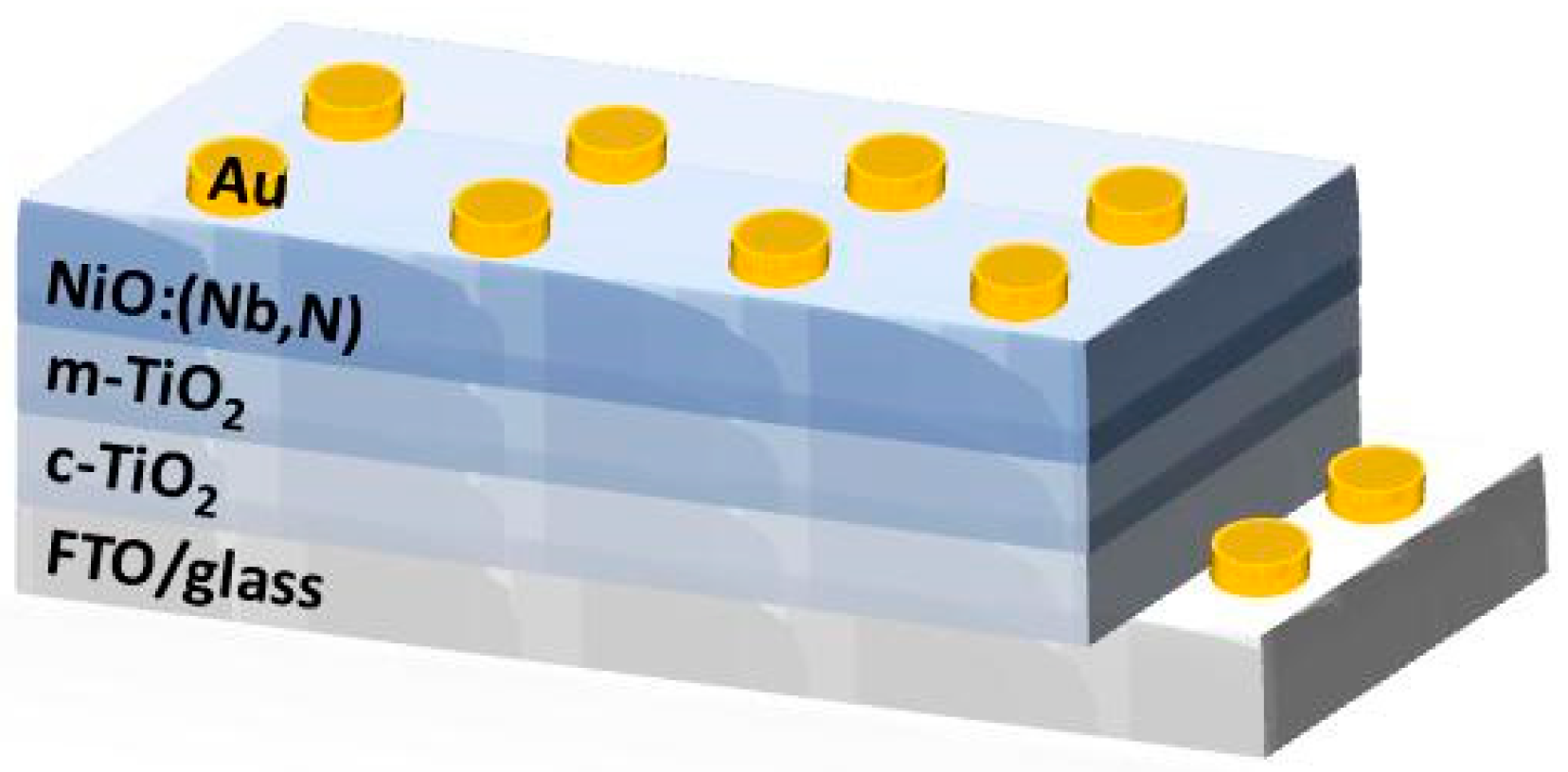
Figure 2.
(a) SEM cross-sectional image of TiO2/FTO/glass. (b) UV-Vis-NIR transmittance of TiO2/FTO/glass (black solid line) and FTO/glass (red dash lines). The Tauc plots for determining the optical energy gap of effective TiO2 are also shown in (b): blue open circles for indirect band gap ((αhv)1/2-vs-E)) and red solid squares for direct band gap ((αhv)2-vs-E)) analysis.

Figure 3.
(a) Wide-scan XPS spectra of undoped NiO -X0 film and double-doped NiO:(Nb,N) -XNN film. (b) and (c) High-resolution N 1s and Nb 3d core levels spectra of double-doped NiO: (Nb,N) -XNN film, respectively.
Figure 3.
(a) Wide-scan XPS spectra of undoped NiO -X0 film and double-doped NiO:(Nb,N) -XNN film. (b) and (c) High-resolution N 1s and Nb 3d core levels spectra of double-doped NiO: (Nb,N) -XNN film, respectively.
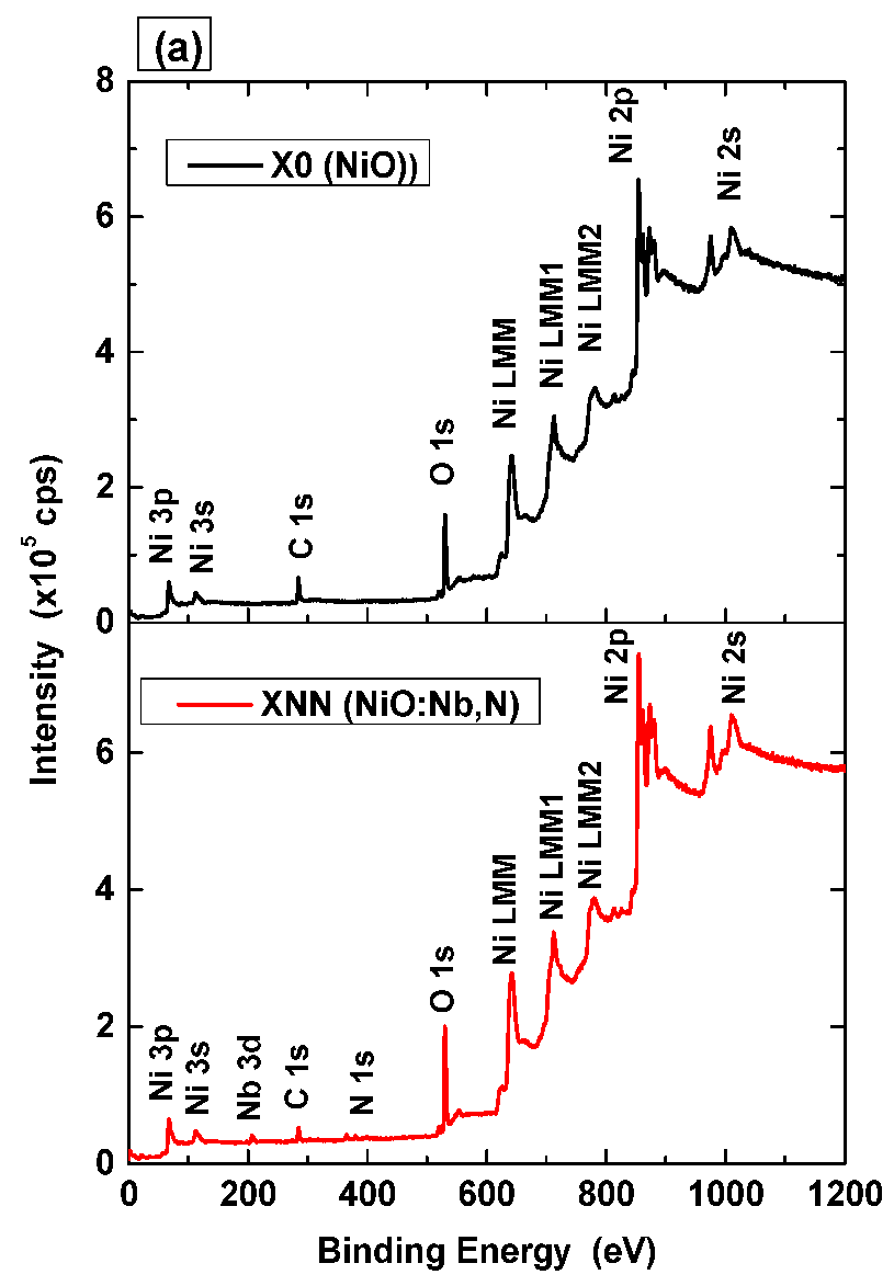
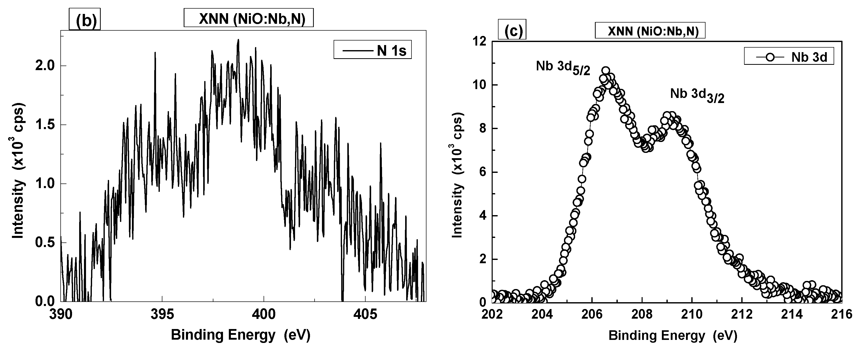
Figure 4.
XRD graphs of (a) undoped NiO –X0 film and (b) doped NiO:(Nb,N) –XNN films deposited on glass substrates just after fabrication and after thermal treatment (TT1).
Figure 4.
XRD graphs of (a) undoped NiO –X0 film and (b) doped NiO:(Nb,N) –XNN films deposited on glass substrates just after fabrication and after thermal treatment (TT1).
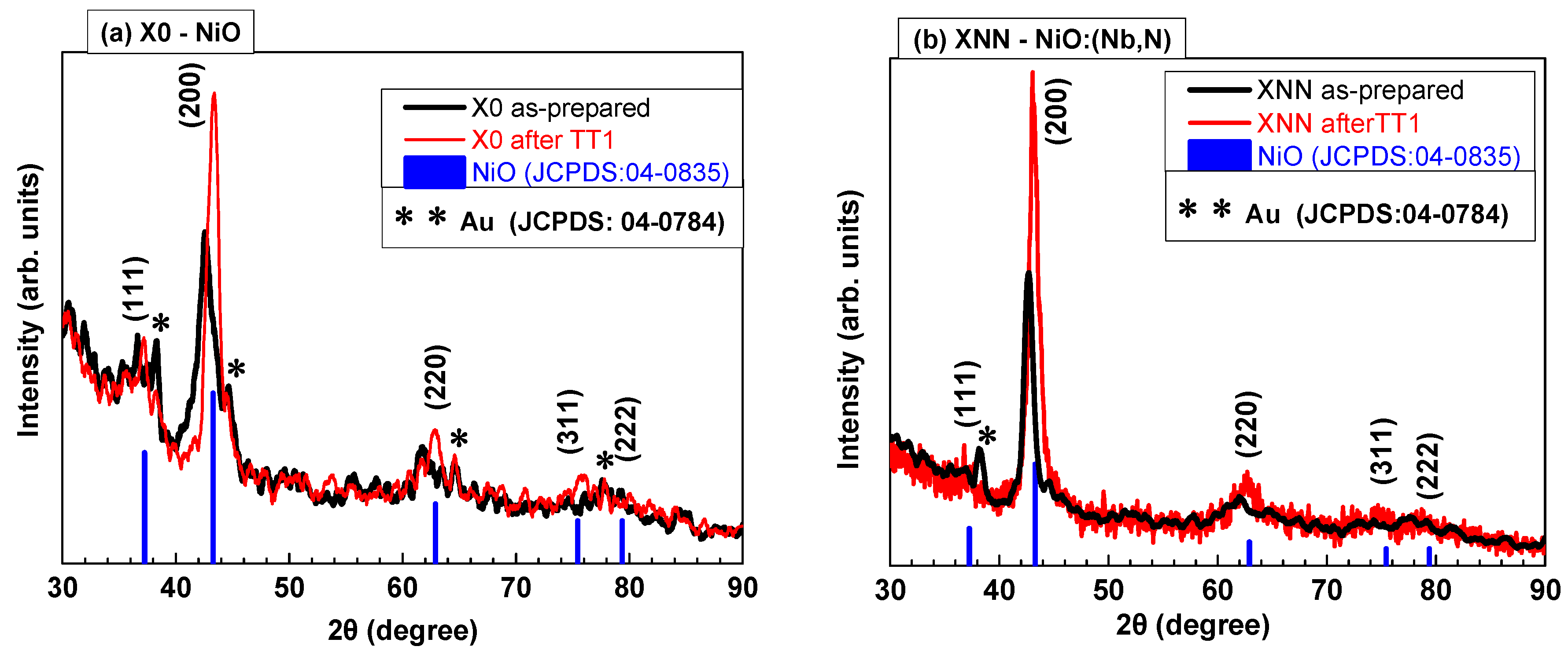
Figure 5.
Topography on the same scale of undoped NiO and double-doped NiO:(Nb,N) films deposited on Si substrates: (a) SEM and (b) AFM images.
Figure 5.
Topography on the same scale of undoped NiO and double-doped NiO:(Nb,N) films deposited on Si substrates: (a) SEM and (b) AFM images.
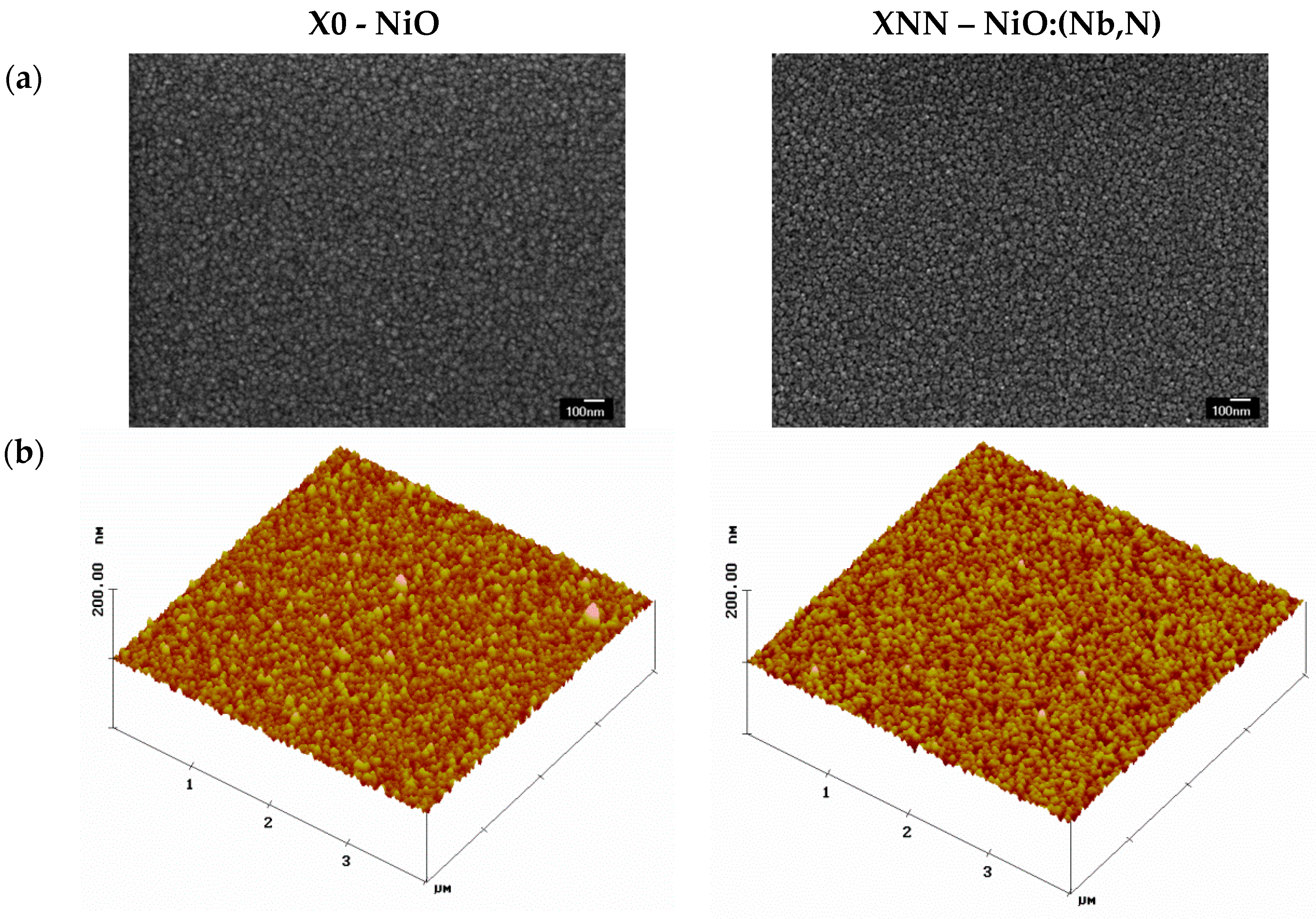
Figure 6.
Optical properties of NiO –X0 and NiO:(Nb,N) –XNN films just after deposition and after thermal treatment (TT1): (a) UV-Vis-NIR transmittance of X0 and XNN films (the arrows indicate the increase of transmittance at λ = 550 nm after TT1). (b) Absorption coefficient, α and ln(α), and (c) Tauc plots of X0 film. (d) Tauc plots of XNN film.
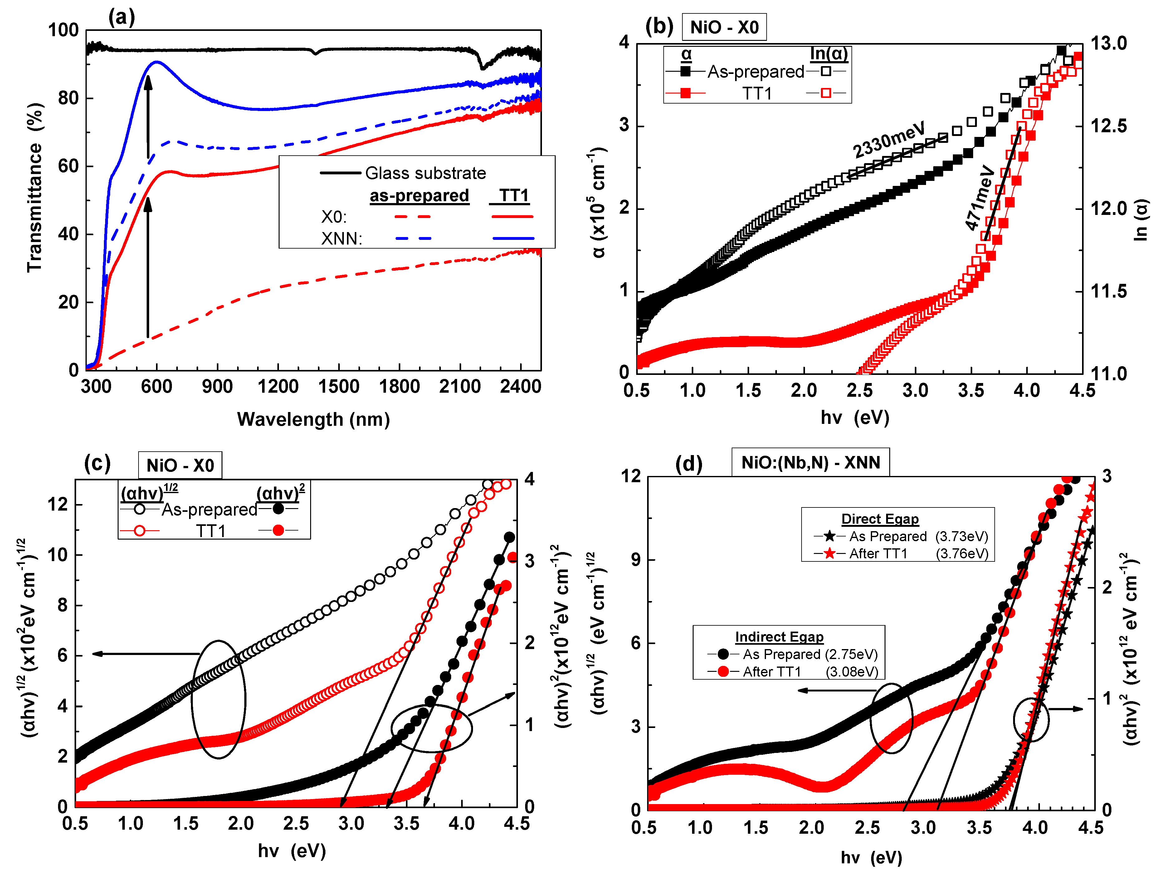
Figure 7.
NiO:(Nb,N)/TiO2 heterostructure: (a) Topography at 30o tilted view and (b) UV-Vis-NIR transmittance before and after TT1, along with the transmittance of substrate (FTO/glass).
Figure 7.
NiO:(Nb,N)/TiO2 heterostructure: (a) Topography at 30o tilted view and (b) UV-Vis-NIR transmittance before and after TT1, along with the transmittance of substrate (FTO/glass).
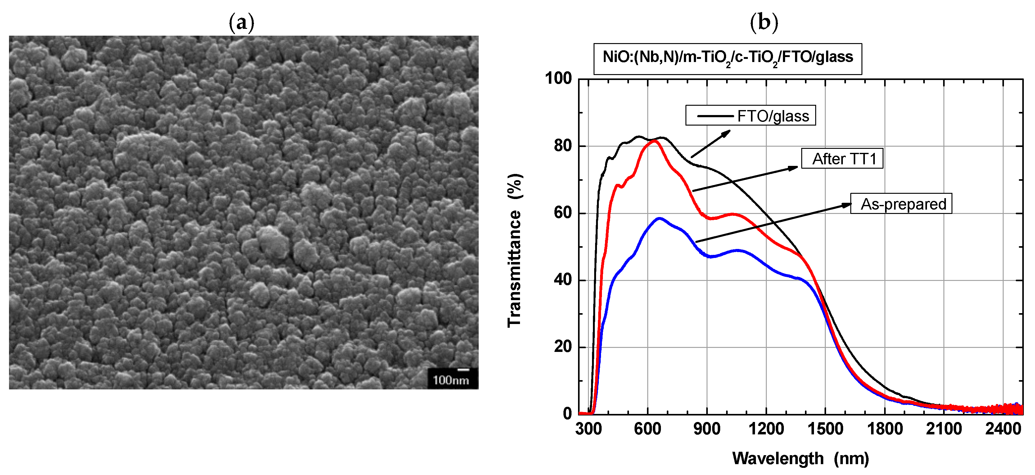
Figure 8.
Current density-voltage J-V characteristics of the NiO:(Nb,N)/TiO2 heterodiode (a) semilog characteristics in the dark (Jd-V)) and (b) linear characteristics in the dark (Jd) and under UV illumination (Jph).
Figure 8.
Current density-voltage J-V characteristics of the NiO:(Nb,N)/TiO2 heterodiode (a) semilog characteristics in the dark (Jd-V)) and (b) linear characteristics in the dark (Jd) and under UV illumination (Jph).
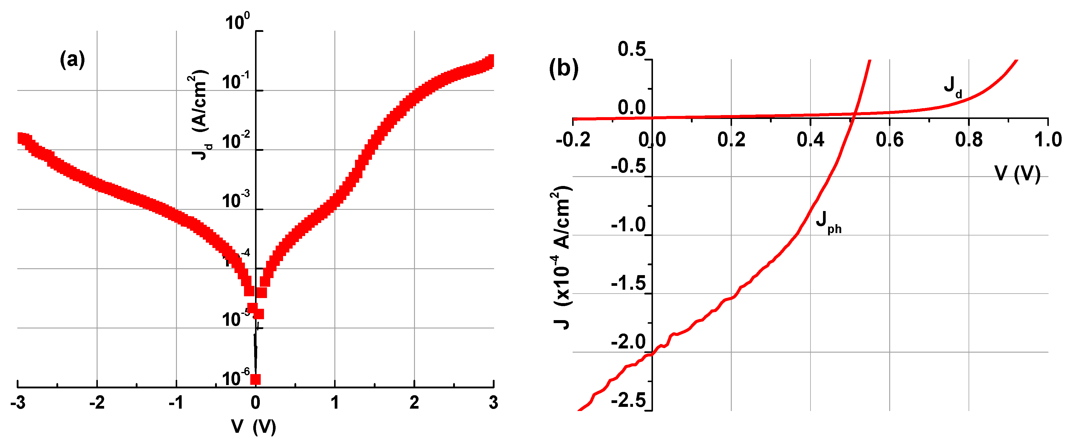

Table 1.
Deposition conditions of: (A) spin-coated TiO2 film (m-TiO2/c-TiO2) and (B) Sputtered NiO-based films.
Table 1.
Deposition conditions of: (A) spin-coated TiO2 film (m-TiO2/c-TiO2) and (B) Sputtered NiO-based films.
| (A) m-TiO2/c-TiO2 films | ||
| Details |
Compact TiO2 – c-TiO2 |
Mesoporous TiO2 – m-TiO2 |
| Spin-coating | HCl:C₂H₆O:C12H28O4Ti=50µL:2.3mL:150µL | TiO2 paste + C₂H₆O |
| Rounds per minute / duration (sec) | 2000 / 30 | 6000 / 30 |
| Thermal treatment | 500◦C / air / 15 min | 500◦C / air / 15 min |
| Thickness (nm) | 40 | 200 |
| Substrates | FTO/glass (2 mm thick glass) | c-TiO2/FTO/glass |
| (B) NiO-based films | ||
| Details |
NiO – Film X0 |
NiO:(Nb,N) – Film XNN |
| Target | Ni | Ni-Nb |
| Gases flow rates | Ar:O2 = 50:50 | Ar:O2:N2 = 50:25:25 |
| Pressure (Pa) | 0.67 | 0.67 |
| Power (W) | 300 | 300 |
| Deposition rate (nm/min) | 1.52 | 1.28 |
| Thickness (nm) | 145 | 130 |
| Target pre-cleaning | 300 W/0.67 Pa Ar/45 minutes | |
| Substrates | Si (100) pieces, fused silica (1 mm thick), TiO2/FTO/glass | |
Table 2.
Crystallographic properties of undoped and double-doped NiO films.
| (200) Peak Position, 2θ (degree) | Crystallite Size, D (nm) | Lattice Strain, ε (x10-3) | Lattice Constant (Å) | ||
|---|---|---|---|---|---|
| X0 - NiO | As-prepared | 42.56 | 5.33 | 17.7 | 4.245 |
| TT1 | 43.40 | 7.44 | 12.4 | 4.166 | |
| XNN – NiO:(Nb,N) | As-prepared | 42.66 | 10.07 | 9.4 | 4.235 |
| TT1 | 43.04 | 9.13 | 10.2 | 4.200 |
Table 3.
Optical properties of undoped NiO -X0, double-doped NiO:(Nb,N) –XNN and TiO2 films. Egap=energy band gap, TT1=thermal treatment, TiO2=m-TiO2/c-TiO2.
Table 3.
Optical properties of undoped NiO -X0, double-doped NiO:(Nb,N) –XNN and TiO2 films. Egap=energy band gap, TT1=thermal treatment, TiO2=m-TiO2/c-TiO2.
| Direct Egap (eV) | Indirect Egap (eV) | Urbach width, EU (meV) | ||||
|---|---|---|---|---|---|---|
| As-prepared | TT1 | As-prepared | TT1 | As-prepared | TT1 | |
| NiO | 3.28 | 3.67 | - | 2.97 | 2330 | 471 |
| NiO:(Nb,N) | 3.73 | 3.76 | 2.75 | 3.08 | 586 | 313 |
| TiO2 | 3.72 | 3.28 | 211 | |||
Table 4.
Selected properties of published NiO/TiO2-based UV-PV thin film devices. SP = Spray Pyrolysis, DC S = DC Sputtering, RTP = Rapid Thermal Processing, TVIS = visible transmittance, PIN = input power, JSC = short circuit current density, ISC = short circuit current, VOC = open circuit voltage.
| p/n layers | Deposition Techn./Thickness | TVIS (%) | λ (nm)/PIN (mW/cm2) | JSC or ISC | Voc (mV) | Year/[Ref.] | |
|---|---|---|---|---|---|---|---|
| p-NiO layer | n-TiO2 layer | ||||||
| NiO/TiO2 | SP | SP | - | Solar Simul./100 | 16.8 mA | 350 | 2018/[5] |
| NiO/SnS/TiO2 | DC S/30nm | DC S/80nm | 40-60 | 365nm/70 | 27.4 μA/cm2 | 765 | 2020/[16] |
| NiO/TiO2 | DC S | DC S+RTP /100nm | 60-70 | 365-520nm/ -- | 0.7-20 μA/cm2 | 25-250 | 2020/[48] |
| NiO/TiO2:N | 30 | DC S+RTP /120nm | 25-45 | 365-520nm/6.5 | 558-66 μA | 130 | 2020/[6] |
| NiO/TiO2 | DC S | DC S+RTP /350nm | 40-55 | 365 nm/30 | 7-8 mA/cm2 | 300-500 | 2021/[47] |
| NiO:Nb/m-TiO2/c-TiO2 | RF MS/150 | Spin coating /240 nm | 55-65 | 325nm/710 | 1.4 μA/cm2 | 200 | 2023/[7] |
| NiO:(Nb,N)/m-TiO2/c-TiO2 | RF MS/130 | Spin coating /240 nm | 70-80 | 325nm/710 | 200 μA/cm2 | 500 | [2024] This work |
Disclaimer/Publisher’s Note: The statements, opinions and data contained in all publications are solely those of the individual author(s) and contributor(s) and not of MDPI and/or the editor(s). MDPI and/or the editor(s) disclaim responsibility for any injury to people or property resulting from any ideas, methods, instructions or products referred to in the content. |
© 2024 by the authors. Licensee MDPI, Basel, Switzerland. This article is an open access article distributed under the terms and conditions of the Creative Commons Attribution (CC BY) license (http://creativecommons.org/licenses/by/4.0/).
Copyright: This open access article is published under a Creative Commons CC BY 4.0 license, which permit the free download, distribution, and reuse, provided that the author and preprint are cited in any reuse.


