
Submitted:
17 October 2025
Posted:
21 October 2025
You are already at the latest version
Abstract
In an attempt to identify solutions to advance net-zero energy actions and accelerate the deployment of cutting-edge low-carbon technologies, hybrid approaches of synthesizing and engineering materials towards solar energy harvesting and management have been developed. In this work, two different forms of TiO2 were synthesized and applied as electron transfer layer (ETL) in perovskite solar cells (PSCs). In addition, double-doped NiO was combined with these two forms of TiO2 and the fabricated NiO/TiO2 heterostructures were examined for their photocatalytic activities against decolorization of methylene blue (MB) probe-molecule pollutant. The two forms of TiO2 were the 1-D TiO2 nanorods (TiO2-NRs), synthesized by an aqueous hydrothermal technique, and the 3-D mesoporous TiO2 (m-TiO2), synthesized by spin-coating. The NiO was fabricated by sputtering and after doping-engineering the optimum double-doped NiO:(Nb,N) was used to form the NiO/TiO2 heterostructures. The PSC formed by the 1-D TiO2-NRs as ETL exhibited under AM1.5 illumination the same open-circuit voltage but twice the short-circuit current when compared to the PSC having the conventional m-TiO2 as ETL. The photocatalytic activity of the 1-D NiO/TiO2 heterostructure with the NRs was 23% faster than the respective 3-D NiO/TiO2 heterostructure, inducing at the same time around 83% more (MB) degradation. The effect of the increased effective surface area of the 1-D heterostructures employing the NRs, along with the enhanced NiO-TiO2 diode properties favouring and enhancing the absorption and the rates of photocatalytic reactions are discussed. These results provide a direct comparison between heterostructures synthesized via hybrid routes for optoelectronic applications in the fields of energy harvesting and photocatalysis.
Keywords:
TiO2 nanorods
; mesoporous TiO2
; NiO:(Nb
; N)
; p/n heterojunction
; perovskite solar cells
; photocatalysis
; oxides properties
; hydrothermal
; spin-coating
; sputtering
1. Introduction
A few decades ago there was the belief that consumption of energy was a figure of merit for civilization and wealth and the associated economic growth had foreseen a sharp increase in demand for energy. The production of energy, however, to fulfil these demands came across technical and environmental obstacles along with the expected increase in worldwide energy costs. The nuclear energy as a possible candidate for power production was faced with scepticism after some serious recent nuclear energy plant accidents (Fukushima, Chernobyl, Three Miles Islands) [1,2], not to mention the long-term disposal problems of the nuclear plants’ wastes. On the other hand, the power production from conventional fossil fuels has been associated with the realized global warming and the climate change accompanied by the extreme weather conditions which are affecting all aspects of human life like health, agriculture and generally everyday life [3]. This has alerted governments and scientists worldwide for the complete decarbonization of the energy system towards a net-zero future by employing a holistic well designed and implemented sustainable, clean, efficient and renewable energy system for the production, manipulation and storage of readily available energy [4]. In an attempt to accelerate the deployment of cutting-edge low-carbon technologies, new approaches for materials’ synthesis and engineering have resulted in the development of a variety of devices like photovoltaics (rooftop, indoor for the Internet of Things, agrivoltaics, bifacial), sensors and photocatalysts for decomposing pollutants and improving air quality, autonomous smart windows for energy-efficient buildings, etc.
Multifunctional nanostructured metal-oxides fabricated by industrially viable and/or low-cost techniques have been employed for fabricating advanced devices for energy harvesting and environmental monitoring. Single layer coatings consisting of n-type oxides (like TiO2, ZnO, In2O3:Sn (ITO), SnO2:F (FTO), etc) or p-type oxides (like Cu2O, NiO2, SnO) have been used for sensing, antibacterial, photocatalytic or chromogenic applications [5,6]. In addition, p/n all-oxide heterostructures have been developed for enhancing sensing, photocatalysts and photovoltaics performance since they are considered promising alternatives to the single layers and very expensive noble metal-based systems. The combination of oxides with various semiconductors like Si, GaAs, GaN, etc, to form heterojunctions for advanced heterostructure concepts with improved properties has also been developed. These advanced heterostructures have been realized by employing hybrid fabrication technologies, where the term “hybrid” refers mainly to the use of two different techniques for synthesizing the two different materials (organics and/or inorganics) of the p/n heterostructures [7]. Such hybrid approaches are made either for realizing novel and innovative ideas as a “proof of concept” or whenever the use of a single deposition technique cannot be used due to technical constraints. Such examples are the dye sensitized solar cells, electrochromic devices, perovskite solar cells, indoor photovoltaics, photocatalysts, electro-optical modulators, solar absorbers, etc [8-11]. The n-type titanium dioxide (TiO2) and the prototype p-type nickel oxide (NiO) are among the most commonly used oxides for these applications. These materials are abundant, low-cost and can be easily synthesized and fabricated. Additionally, they possess versatile physicochemical properties [12,13]. In addition, they can be formed by chemical methods and various other non-chemical deposition techniques like sputtering, atomic layer deposition, pulse layer deposition, etc, as continuous thin films (3-D), 2-D layers or 1-D structures (nanowires, nanorods, etc) and depending on the application, their properties can by adjusted by selectively modifying the deposition parameters and applying doping engineering by adding the appropriate elements [14,15].
In this work metal oxides were synthesized to realize hybrid heterostructures, namely perovskite solar cells and photocatalysts. TiO2 nanorods (TiO2-NRs) were made by a hydrothermal method and mesoporous TiO2 (m-TiO2) were formed by spin-coating and used as electron transfer layer (ETL) in perovskite solar cells. In addition, the synthesized TiO2 structures (TiO2-NRs and m-TiO2) were integrated with another metal oxide layer, namely the NiO, deposited by sputtering after doping-engineering. This resulted in p-NiO/TiO2 heterostructures, which were examined for their photocatalytic performance. There have been very few comparisons reported in the literature between TiO2-NRs and m-TiO2 as ETLs in perovskite solar cells [16]. Furthermore, TiO2-based hybrids have been reported with different junction schemes and doped elements either inside the Ti-O matrix or metallic species on the surface and having a variety of morphologies [15]. The synthesized metal oxides in this work were examined for their physicochemical properties and the hybrid photovoltaic and photocatalytic heterostructure devices with the different architectures were tested for their output characteristics. The properties of the oxide materials and devices were compared, highlighting both the observed improvements and the limitations of their potential applications.
2. Materials and Methods
2.1. Oxides Synthesis and Characterization
The substrates used to form mesoporous TiO2 (m-TiO2) and nanorods TiO2 (TiO2-NRs) were commercially available FTO-coated glasses. However, since both TiO2 architectures were intended to serve as an electron transfer layer (ETL) in perovskite solar cells the use of a thin precursor TiO2 layer was necessary to be placed on top of the FTO layer. The thin TiO2 layer would serve as a compact layer to eliminate the contact of the perovskite layer with the highly conductive FTO-covered glass substrate. In addition, the same thin TiO2 layer would serve as a seed layer providing the preferred nucleation sites for the growth of TiO2 nanorods [17]. The thin TiO2 layer, which serves as both seed and compact layer, will be called thereafter as s-TiO2. Prior to deposition, the FTO-coated glasses were cleaned in a standard procedure utilizing an ultrasonic bath: 10 minutes in acetone, 10 minutes in isopropanol followed by rinsing in deionized water and dried in N2 gas flow. After the cleaning process, the s-TiO2 layer was formed by means of spin coating. A TiO2-containing solution (50 μL of hydrochloric acid, 2.3 mL of ethanol and 150 μL of titanium isopropoxide) was stirred for several hours and was spin-coated (2000 rpm, 30 sec) on the FTO/glass substrates. This way, a 40 nm thick s-TiO2 film was formed, which was thermally treated at 500 °C for 15min in air. The TiO2-NRs were made by an Aqueous Chemical Growth (ACG) technique on the s-TiO2/FTO/glass substrates and a schematic representation is seen in Figure 1a. The growth solution was prepared by dissolving 10 mL hydrochloric acid (37 wt%) in 10mL of deionized water under magnetic stirring. After 10 minutes of stirring, 340 μL of titanium isopropoxide (97%) was added. Hydrothermally TiO2 nanorods growth was carried out by suspending the 3D structures with an angle and the coated side was kept face down in a Teflon-lined stainless-steel autoclave (50mL) filled with the growth solution. The autoclave containing the substrate was sealed and annealed inside an oven at 175 OC for 3h. After that, the autoclave was cooled to room temperature under tap water. The substrate was finally washed with deionized water and dried in air for 15 minutes [18, 19]. No further heat treatment was applied for the TiO2-NRs/s-TiO2/FTO/glass structures.
The mesoporous TiO2 (m-TiO2) films were fabricated by means of spin coating on the s-TiO2/FTO/glass substrates, which schematically has been depicted in Figure 1b. The substrates were plasma treated in oxygen and then a commercially available TiO2 mesoporous paste (Titania paste, ~50 nm nanoparticles, Sigma Aldrich), with around 50 nm TiO2 nanoparticles, was diluted in ethanol (weight ratio 1:7), stirred for several hours to obtain a completely homogeneous solution and spin-coated (6000 rpm, 30 sec) on top of the substrates in the ambient. The m-TiO2 layer was formed to be around 170 nm thick as it was the optimum thickness for an ETL in perovskite solar cells. The procedure was completed by annealing the m-TiO2/s-TiO2/FTO/glass structure at 500 °C for 15 min in air.
The NiO layers, employed as the p-type oxides to cover the m-TiO2 and TiO2-NRs films and form the heterostructures for photocatalytic evaluation, were deposited by sputtering. The undoped NiO layer was formed from a metallic Ni target in plasma containing 50% Ar : 50% O2 gases [20], whereas the doped NiO layer was formed from a Ni-Nb composite target in plasma containing 50% Ar : 25% O2 : 25% N2 gases [21]. The composite target consisted of the Ni target on which Nb pellets were placed. In this way double-doped NiO:(Nb.N) could be obtained. All depositions were made at a total pressure of 5 mTorr, rf-power of 300 Watts on unintentionally heated substrates which were at a distance of 10 cm above the target. All NiO films underwent a post-deposition heat treatment at 300 oC for 15 minutes in flowing N2. The thickness of the NiO films was around 150 nm. Details on the fabrication procedure of sputtered NiO can be found elsewhere [22].
Characterization of Materials
The materials synthesized in this work were characterized employing the typical techniques generally used for oxides. More precisely, Energy-Dispersive X-ray (EDX, Oxford Instruments- INCA system) and X-Ray Photoelectron Spectroscopy (XPS, SPECS Flexmod system) were employed to confirm the existence of dopants in NiO films. Field-Emission Scanning Electron Microscopy (FE-SEM, Jeol JSM-7000F system) and Atomic Force Microscopy (AFM, Digital Instruments-Multimode system) for examining the surface morphology of the films. Grazing Incidence X-ray Diffraction (GIXRD) was used (Bruker D8 ADVANCE system) at grazing incidence (1.6 O), with a rate of 0.02 O/sec over the range of 30–90O for identifying the crystallographic phases in the oxide structures and extracting the crystallite size (D) and lattice stain (εL) through the equations (1) and (2), respectively [23]:
where k is the shape factor 0.94, λ is the wavelength of incident radiation 1.5406 Å, hkl represents the Miller indices of the diffraction plane, βhkl is the full-width at half-maximum (FWHM), and θ is the Bragg angle of the peak.
D = kλ/βhklcosθ
εL = βhklcotθ/4
The UV-Vis-NIR transmittance was monitored in the wavelength range of 250 to 1200 nm (Perkin Elmer Lambda 950) for extracting the absorption coefficient (α), from which the direct band gap was determined through the equations (3) and (4) [24]:
where, T is the transmittance, α is the absorption coefficient, d is the thickness, h is the Planck constant, v is the frequency, n=1/2 for the direct gap and Egap is the optical band gap. Resistivity measurements were made through the 4-probe van der Pauw technique on films having cross patterns and the type and concentration of carriers were determined for selected films through the ac-modulated Hall effect measurements. The thickness of the 1-D films (nanorods) was determined through cross-sectional SEM images, whereas the thickness of the 3-D films was measured by a Veeco Dektak 150 profilometer.
T ~ exp(-αd)
(αhv) = A (hv − Egap)n
2.2. Fabrication and Characterization of Devices
After the formation of the m-TiO2 and TiO2-NRs on s-TiO2/FTO/glass substrates, as described above, the perovskite solar cells were completed by depositing the perovskite and the hole transfer layer (HTL) materials. The perovskite material was FA0.8MA0.04Cs0.16Pb(I0.5Br0.5)3 and 5% PbCl2 was added in the precursor as an additive and N2 gas was used for quenching [25]. The perovskite was dissolved in dimethylformamide (DMF) and dimethyl sulfoxide (DMSO) solution (DMF:DMSO = 4:1), spinned at 3000 rpm for 40 sec and the N2 gas started flowing after the 10th sec (1.5 mbar at 1.5 cm distance from the substrate). The procedure was accomplished by heat-treating the film at 120 oC for 10 min, while the Spiro-OMeTAD (2,2',7,7'-Tetrakis[N,N-di(4-methoxyphenyl)amino]-9,9'-spirobifluorene) was used as HTL material. A solution containing 144.6 mg SPIRO OMeTAD, 57.6 μL Pyridine, 57.6 μL Li-TFSi (520mg/1ml Acetonitrile) and a 58μL FK-209 (300mg/1mL Acetonitrile) in a 1mL Chlorobenzene solvent was spin-coated (3000 rpm, 40 sec) on the substrates. No extra thermal treatment was applied to the formed layer which was exposed to the ambient for further oxidation for an optimized period of time depending on humidity and temperature. It should be mentioned that the fabrication of the devices were made in the ambient and not in a controlled glove-box N2 environment, which is the common fabrication practice for high efficiency perovskite solar cells. A shadow mask was used for applying by sputtering the Au pads (5 mm x 5 mm) as ohmic contacts on the HTL and FTO layers. A schematic representation of perovskites solar cells having mesoporous (m-TiO2) and nanorods (TiO2-NRs) as ETL is shown in Figure 2a,b, respectively. The characterization of the solar cells under illumination was carried out under AM1.5 (1000 W/m2) and the open circuit voltage (VOC), short circuit current (JSC), fill factor (FF) and energy conversion efficiency were extracted.
The NiO/TiO2 heterostructures, which were synthesized for testing their photocatalytic activity, were formed by transferring the m-TiO2/s-TiO2/FTO/glass and TiO2-NRs/s-TiO2/FTO/glass substrates into the sputtering chamber for the deposition of p-NiO films as described previously. As an ohmic contact, sputtered Au metal was used for both the NiO and the FTO layers, using a specially designed shadow mask, which defined the junction area of the diode (7.8x10⁻³ cm2). A schematic representation of the NiO/m-TiO2/s-TiO2/FTO/glass and NiO/TiO2-NRs/s-TiO2/FTO/glass heterostructures is shown in Figure 2c,d, respectively. The photocatalytic performance of the NiO/TiO2 devices was evaluated through the degradation of a common probe pollutant such as methylene blue (MB) through its decolorization per time Ct/CO x100 %, where CO is the initial MB concentration and Ct is the concentration after a time interval t. The MB was first tested in a blank experiment (photolysis) without the presence of the heterostructures/catalysts. The experiments were conducted in a 100 ml beaker under simulated solar light provided by a 500 W halogen lamp. The photocatalysts were immersed in 100 ml aqueous solution of the pollutant, and the light source was positioned approximately 20 cm away from the solution, generating an intensity of approximately 1000 W/m2 at the beaker's surface, equivalent to one sun. Before irradiation, the solution was stirred for 30 min in the dark to achieve adsorption-desorption equilibrium. Following this, the light was turned on, and a portion of 5 ml were extracted at specified time intervals and centrifuged to monitor the degradation process. The photocatalytic degradation of the MB concentration was quantified by estimating the apparent rate constant (K) of the reaction according to equation (5):
ln(Ct/CO) = -Kt
Details of the experimental set-up for the photocatalytic activity measurements can be found elsewhere [26].
The heterodiode devices were tested for their UV-Vis-NIR transmittance, as described in subsection 2.1.4 Characterization of materials, and the current–voltage (I-V) characteristics were recorded using the Agilent 4200-SCS unit. The characteristics of the hybrid heterostructures (perovskite solar cells and NiO/TiO2 photocatalysts) in the dark, such as saturation current (IS), barrier height (Φb), ideality factor (n) and series resistance (RS), were obtained following thermionic emission theory from the I–V curve. Details of the procedure for extracting the diode parameters from the I-V curves can be found elsewhere [20,27].
3. Results and Discussion
In this section the basic properties of the synthesized 1-D and 3-D TiO2 materials (TiO2-NRs and m-TiO2, respectively) are presented, and this will be followed by the properties of the formed devices, i.e. perovskite solar cells and p-NiO/n-TiO2 heterostructures photocatalysts, where the TiO2 material was served as electron transfer layers (ETLs) for the former device and n-type layers for the latter device.
3.1. Properties of m-TiO2 and TiO2-NRs Materials
As mentioned previously, the m-TiO2 was synthesized so to have a thickness of around 170 nm, as this is the optimum thickness for m-TiO2 so to serve as ETL in perovskite solar cells [25]. This was the thickness of the 3-D m-TiO2 layer used for the solar cells and the photocatalytic devices presented in this work while no attempts were made to investigate the effect of m-TiO2 thickness on the performance of the devices. Figure 3a presents the typical surface morphology of the m-TiO₂ layer, obtained by AFM, from which the RMS roughness was determined to be approximately 20 nm. The structure of the m-TiO2 layer contained a mixture of anatase and rutile crystalline phases, as seen in Figure 3b, which shows the XRD pattern of the m-TiO2/s-TiO2/FTO/glass configuration, along with that of the FTO/glass for comparison reasons. It is seen that the XRD pattern is mainly dominated by the strong peaks arising from the 600 nm thick FTO layer. In addition, the visible transmittance of the m-TiO2/s-TiO2/FTO/glass configuration was 70–80%, from which the effective direct optical Egap was determined to be 3.72 eV. A full account of the properties of the TiO2 layer can be found in Ref. [20]. The UV-Vis-NIR transmittance of the 3-D structure is depicted in Figure 5b along with that of the 1-D structure.
The dimensions of the synthesized 1-D TiO2-NR depended on the time of formation of the NRs by the hydrothermal technique. By increasing the formation time, the diameter and the height (length) of the TiO2-NRs increased. Figure 4 shows the top-view SEM images of TiO2-NRs after 40 min, 60 min and 80 min of formation. The TiO2-NRs after 80 min of growth were almost vertically aligned and each rod had a square-shaped geometry with a size of almost 100x100 nm. The height of the NRs was around 150 nm, 300 nm and 600 nm after 40 min, 60 min and 80 min of growth, respectively.
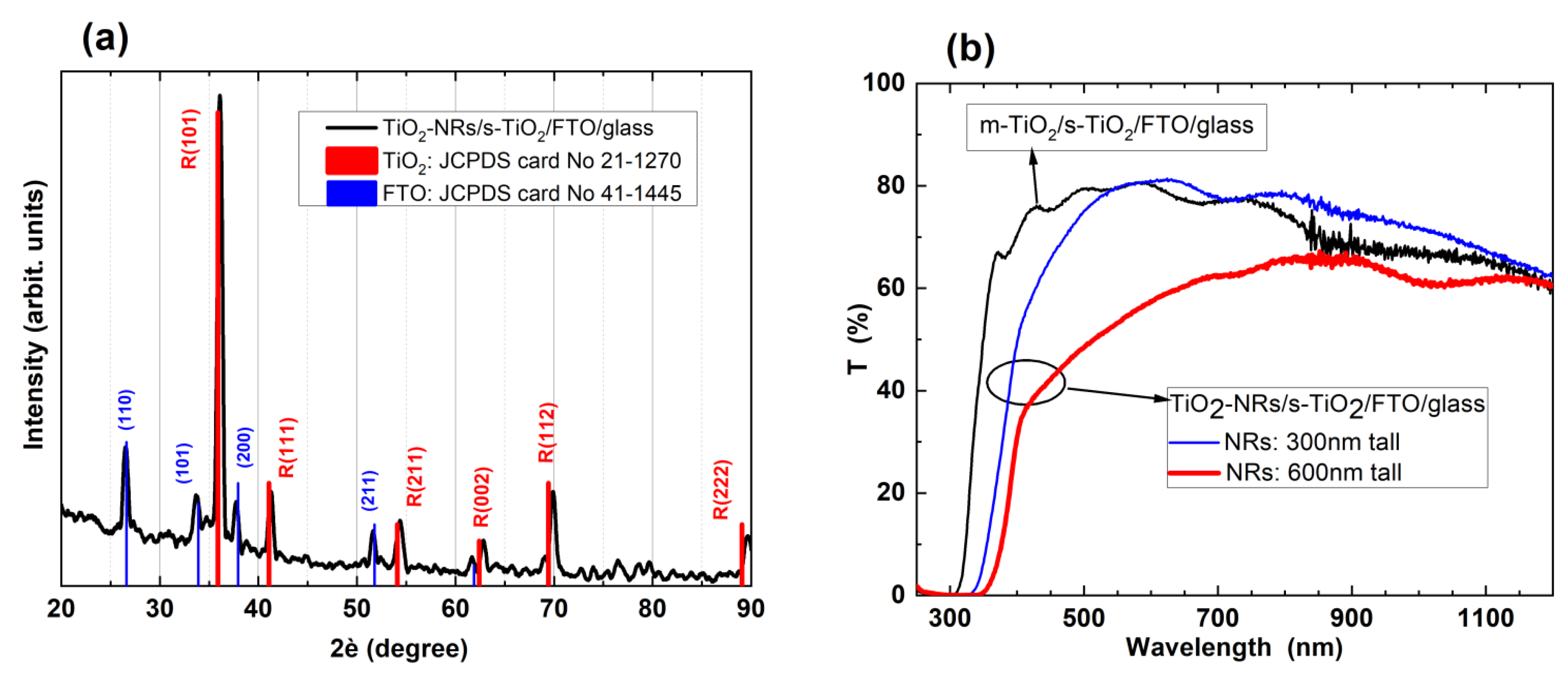
The GIXRD pattern of the TiO2-NRs/s-TiO2/FTO/glass structure is seen in Figure 5a. In contrast to the m-TiO2 layer seen above, the TiO2-NRs were crystallized in the rutile phase (JCPDS card No: 21-1276) [28]. By employing EDX analysis it was revealed that the chemical composition of the NRs was in atomic percentages: Ti = 27.74% and O = 73.26%, which is very close to 2 (O:Ti=2.6) for stoichiometric TiO2, taking into account the limited accuracy of EDX. The UV-VIS-NIR transmittance of two 1-D structures having different NR heights was monitored and the results are depicted in Figure 5b, along with the transmittance of the 3-D structure (m-TiO2/s-TiO2/FTO/glass) for comparison reasons. As seen in Figure 5b the onset of absorption shifts to longer wavelengths (decrease of the effective Egap) for the 1-D structure when compared to the 3-D structure, from 333.3 nm (3.72 eV) to 380.4 nm (3.26 eV). It should be mentioned that for the determination of the NRs effective Egap, the s-TiO2/FTO/glass configuration was considered as substrate, as for the case of m-TiO2 mentioned previously. In addition, as the height of the nanorods increases from 300 nm to 600 nm the visible transmittance was reduced, by around 37% at λ=550 nm (from T=80% to T=55%), accompanied by a shift of absorption energy to longer wavelengths. This behaviour could be attributed to the non-uniform distribution and the high aspect ratio of the NRs, which resulted in reduced back-reflection and the increased absorption of incident light in the rutile phase being the dominant one in the structure [29].
Figure 5.
(a) XRD pattern of TiO2 nanorods and (b) UV-VIS-NIR transmittance of TiO2 nanorods having two different heights, along with the transmittance of m-TiO2.
Figure 5.
(a) XRD pattern of TiO2 nanorods and (b) UV-VIS-NIR transmittance of TiO2 nanorods having two different heights, along with the transmittance of m-TiO2.
3.2. Perovskite Solar Cells with m-TiO2 and TiO2-NRs as ETL
After examining the properties of the m-TiO2 and TiO2-NRs, the fabrication of the perovskite solar cells (PSCs) were realized, having as ETL the two different architectures of TiO2, namely the standard one of spin-coated mesoporous TiO2 (m-TiO2), which served as the reference PSC and the hydrothermally made TiO2 nanorods (TiO2-NRs). The PSC devices with the m-TiO2 ETL will be called thereafter as 3-D PSC, whereas the respective one with the TiO2-NRs will be called 1-D PSC. Two different 1-D PSCs were examined having 300 nm tall NRs (PSC1) and 600 nm tall NRs (PSC2). The main goals for examining these PSC structures were to: (i) achieve photovoltaic behaviour for the 1-D PSC devices, (ii) increase the effective area of the TiO2/perovskite interface, (iii) take advantage of the improved transport properties of the TiO2-NRs with enhanced structural quality, (iv) enhance electron transport, (v) reduce recombination of photogeneration carriers and (vi) to eliminate shunting paths of carriers between HTL and FTO layers [30-33]. It should be mentioned that 1D-PSC having NRs taller than 600 nm were not examined since preliminary experiments showed that the respective PSCs could not exhibit any photovoltaic behaviour. Figure 6 shows the cross-sectional SEM images of PSCs having as ETL the conventional m-TiO2 (Figure 6a, 3-D PSC) and the TiO2-NRs (Figure 6b, 1-D PSC1 300 nm tall NRs and Figure 6c, 1-D PSC2 600 nm tall NRs). The different morphology of the perovskites grown on top of the 1-D and 3-D ETLs is attributed to the different surface morphologies and uniformities of the ETLs as shown in Figure 3 and Figure 4, respectively. However, as seen in Figure 6b,c, even though the perovskite layers maintained the low uniformity of the TiO2-NRs, the HTL on top of the perovskite layers reduced the final roughness of the PSC.
The current density-voltage characteristics of the PSC in the dark (Jd-V) and under AM1.5 illumination (Jph-V) are seen in Figure 7a,b, respectively. All Jd-V curves of the devices in the dark show a shift of the minimum dark density current, Jd, with respect to the applied voltage. This shift is towards negative voltages for the 3-D PSC and to positive voltages for the 1-D PSCs. It is also observed in Figure 7a that the NRs with the lower height (300 nm, PSC1) exhibit the largest shift of the minimum Jd to positive V. The existence of ionic charges in the PSC layers is responsible for the observed shift, but more experiments associated with the transport of carriers in these 1-D and 3-D PSC are needed to clarify the reason for this phenomenon of the opposite shift of the Jd-V curves with applied voltage for the PSC devices [31,34,35]. The diodes parameters, as extracted from the Id-V curve of Figure 7a, are depicted in Table 1. The 3-D PSC diode showed better characteristics than the 1-D PSC diodes, concerning the ideality factor and the series resistance values (n=2.31 and RS=0.16 kΩ). In addition, the 1-D PSC2 device with the highest NRs (600 nm) showed lower ideality factor and series resistance values (n=4.0 and RS=3.25 kΩ) than the respective one with the NRs having lower height (300 nm, 1-D PSC1). The behaviour of the devices under AM1.5 illumination is shown in Figure 7b. Comparing the two 1-D PSCs, the PSC2 (tallest NRs) showed better performance than the PSC1 (shorter NRs) concerning JSC, VOC, and efficiency. Even though the TiO2-NRs with the highest NRs had reduced visible transmittance when compared to the one with the shorter NRs, as seen in Figure 5b, the high JSC is likely associated with the reduced reflectance due to the high aspect ratio of the highest NRs, resulting in enhanced photon absorption and consequently increased JSC. It is known that JSC of 1-D PSCs strongly depends on NRs length [30,31]. There is an optimum TiO2-NRs length where the spin-coated perovskite layer on top of the NRs fills the gaps and the voids of the NR matrix to achieve maximum electron injection, transport and extraction and thus maximum Jph for the hybrid PSCs. The NRs length of around 600 nm was the optimum one for the 1-D PSC fabricated in this work, which is consistent with similar reports in literature [30]. It has been recognized that the diameter, length and density distribution of the NRs must be carefully tuned to achieve an ideal perovskite-TiO2-NRs interface, thereby enabling faster electron extraction compared to the m-TiO2 film and enhancing the photovoltaic performance of TiO2-NR based PSC [31]. The low FF of the 1-D PSC2 device is associated with the observed knee in the JSC curve, which is generally observed for PSCs and is associated with the trapping of carriers at the interface [35,36]. In our case, the knee seen in the 1-D PSC2 could also be due to the enhanced granule-like formation of the perovskite layer on top of the NRs as seen in Figure 6c. Finally, as expected, the 1-D PSC with the nanorods as ETL gave the same VOC but higher JSC by a factor of two when compared to the 3-D PSC with the mesoporous ETL due to the increased effective area of the TiO2-NRs/perovskite interface and the improved transport properties of the TiO2-NRs with the enhanced structural quality.
It should be mentioned that the low performance of the presented PSCs is attributed to the low performance of the reference 3-D PSC having the conventional m-TiO2 as ETL. This was due to the fabrication procedure used for the PSCs which was in the ambient and not in an inert environment, as described in the Experimental Procedures section. Nevertheless, the 1-D PSC2 having 600 nm tall NRs as ETL showed twice the JSC than that of the conventional 3-D PSC. It is anticipated that the elimination of the knee seen at the Jph-V curve of the 1-D PSC1 devices (Figure 7b) will increase FF and consequently the conversion efficiency of the 1-D PSC2 by at least a factor of two than that of 3-D PSC [30,31].
3.3. Photocatalytic NiO/TiO2 Heterostructures with m-TiO2 and TiO2-NRs as n-Type Layer
Even though the TiO2 material, either in 1-D or 3-D forms, which was employed in the formation of the NiO/TiO2 heterostructure for investigating its photocatalytic properties, was used without any post-deposition treatment or any intentional doping, this was not the case for the p-NiO material. It is widely recognized that the photocatalytic reaction mechanism is based on the band theory of solids. The standard mechanism of photocatalysis is the production of many photogenerated holes and electrons (photocarriers) under light irradiation. In addition, it is known that heterojunction photocatalysts composed of two different semiconductors are considered the most promising photocatalysts since they can exhibit enhanced photocatalytic activity and photostability [7]. This is based on the reduced recombination rate of photogenerated carriers, which can be achieved by doping engineering of the heterostructure layers, modifying the band structure, enhancing the electrostatic built-in field at the heterostructure interface and thus improving the charge transport and the separation and migration speed of the photocarriers [38]. For these reasons, the initial fabricated undoped NiO film was selectively doped to modify its properties and enhance the NiO/TiO2 heterodiode properties. The fabricated NiO was a p-type disordered structure, which after optimizing with nitrogen (N) doping, its disorder was improved resulting in increased resistivity and transparency when compared to the undoped NiO [24]. In addition, niobium (Nb) doping of NiO reversed the properties created by the N-doping mentioned above [39]. By co-doping of NiO with both N and Nb dopants improved the overall properties of the undoped NiO or the single-doped NiO:Nb and NiO:N materials. The improvement in the NiO structure involved reduced roughness, increased crystalline size, reduced strain and reduced tail states. The existence of both Nb and N dopants in the NiO structure was verified by the XPS experiments on undoped NiO and double-doped NiO:(Nb,N) seen in Figure 8 for films which were deposited on Si substrates. Preliminary analysis of the XPS spectrum showed that the atomic percentage of Ni, O, Nb and N were 49.9, 46.2, 1.8 and 2.1, respectively. The basic structural, optical and electrical properties of the NiO:(Nb,N) are seen in Table 2, before and after thermal treatment (TT1), along with the undoped NiO for comparison. It should be mentioned that the properties of the NiO and NiO:(Nb,N) tabulated in Table 2 were extracted from films which have been deposited on glass substrates. The superior properties of the optimized p-NiO:(Nb,N) material were manifested when the thermally treated material was used as p-type layer in p-NiO:(Nb,N)/n-TiO2 which exhibited enhanced UV-PV properties when compared to both undoped and single-doped NiO materials [22]. This implied that the conduction of the carriers throughout the p/n device is not inhibited, the carriers were not trapped in defects or states, the built-in voltage is enhanced and all carriers were effectively collected. The double-doped NiO:(Nb,N) used for the photocatalysis experiments will be called thereafter as NiO.
A 190 nm thick sputtered NiO:(Nb,N) layer was deposited on the 1-D TiO2-NRs and the 3-D m-TiO2, which had been formed on s-TiO2/FTO/glass substrates as mentioned in section 2.1, so the NiO/TiO2 heterostructures were tested for their photocatalytic properties. The morphology of the TiO2-NRs and m-TiO2 surface before and after the deposition of the NiO layer is seen in the SEM images of Figure 9. It is seen in Figure 9a that the around 600 nm tall TiO2-NRs were almost vertically aligned. Furthermore, the 190nm-thick sputtered NiO seen in the Figure 9a1,a2 top view or 30o tilted images, respectively, could cover more than one NR and the spheroids formed on top of the NRs after the NiO deposition exceeded their diameter [40,41]. In a separate experiment employing image analysis of the SEM images, the nanorods’ diameter was determined to be 97±10 nm [40]. In addition, the diameter of the spheroid-like NiO material on top of the NRs was calculated to be 151±17 nm with a lateral NiO thickness on the NRs side-walls to be 27±7 nm. It is anticipated that the step-coverage which can be achieved by the sputtering deposition technique ensures that the NiO layer is able to cover conformally the entire nanorods, through the intrusions and reaching down to the TiO2 seed layer [40,42].
The situation was different with the 3-D m-TiO2 layer, which had already formed a continuous layer by the spin-coating technique, as seen in Figure 3. Upon NiO deposition by sputtering, big nodules were formed having a lateral dimension of up to 200 nm. The different surface morphologies and structural properties of the NiO/m-TiO2 and NiO/TiO2-NRs were reflected in the dark J-V characteristics of the heterostructures in the dark as well as in their photocatalytic behaviour, as will be seen next.
Figure 10 shows the dark Jd-V characteristics of the 1-D and 3-D NiO/TiO2 heterostructures, whereas after analyzing the Jd-V curves, the diodes’ properties are tabulated in Table 3. As seen in Figure 10, both heterostructures show rectification. However, the minimum dark current density (Jd) for the NiO/m-TiO2 occurs at zero applied voltage whereas the respective Jd value of the NiO/TiO2-NRs diode has been shifted to positive voltage (around 1.7 V). The shift of the minimum Jd to positive voltages was also seen in Figure 7a for the case of the 1-D and 3-D PSCs. This phenomenon generally appears when oxides are used to form hybrid heterostructures and it has been attributed to the formation of a dipole at the diode’s interface [34,43,44]. The 1-D NiO/TiO2 diode shows better properties than the 3-D NiO/TiO2 diode: the saturation current density (JS) was five orders of magnitude lower, the series resistance (RS) values was lower by a factor of 2.8, the barrier height (φb) was 1.5 times higher and the ideality factor (n) took the value of almost 2 which was three times lower than the value of the 3-D diode. The improved diode properties of the 1-D structure are attributed to the better quality of the TiO2 nanorods than the mesoporous TiO2. Despite the hybrid way of synthesizing the heterostructures, ideality factor values much greater than two have been reported for various heterodiodes like all-oxide diodes [21,45], oxides grown on epitaxial layers [46] or non-oxide epitaxially grown structures [47] and have been attributed to transport mechanisms through recombination at defects/states at the interface, tunneling through the interfacial layer, or space charge current transport. The enhanced surface morphology and the diode parameters of the 1-D heterostructure resulted in better photocatalytic behaviour than the 3-D heterostructure.
As mentioned in the Experimental Details section (§2.2), the photocatalytic performance of the 1-D and 3-D NiO/TiO2 heterostructures was studied by recording the decolorization of methylene blue (MB), which is a typical potent cationic dye widely used as a model organic probe to test the photocatalytic performance of catalysts, under UV irradiation. The decrease of MB concentration was recorded for the NiO/TiO2 structures, having both of them an effective active surface area of approximately 5 mm2. The time evolution of MB concentration under UV irradiation for the 1-D and 3-D structures is shown in Figure 11. The photolysis curve (black curve in Figure 11), recorded in the absence of the photocatalysts, is also displayed for comparison reasons. No change in the concentration of the dye solution was observed, confirming the high resistance of MB to direct photodegradation. This result also confirms that MB photodegradation occurs on the 1-D and 3-D nanostructured material surface and is attributed to the reaction of MB with highly oxidative radicals generated on the surfaces under UV irradiation. As clearly seen, the highest decrease occurs in the case of 1-D structure with the TiO2 nanorods (blue star symbols in Figure 11) compared to the 3-D nanostructure with the mesoporous TiO2 (open circle red symbols in Figure 11). In particular, after 60 min irradiation, the 1-D structure with the NRs induced around 83% degradation of the MB, whereas the 3 -D structure induced around 68% degradation. To quantify the photocatalytic degradation of MB concentration, the apparent degradation rate constant (K) of the reaction has been estimated, according to the Eq.5, as seen in the inset of Figure 11. The good linear fit of the experimental data to the above equation confirms that the photodegradation of MB on the heterostructure containing the TiO2-NRs follows pseudo-first-order kinetics [26].
However, since it is known that NiO has no effect on degrading the MB pollutant [48] the observed decolorization of the MB solution is attributed to the NiO/TiO2 heterostructure. The formed built-in field at the NiO-TiO2 interface favoured the separation and electronic mobility of the photo-generated electron-hole pairs. The superior photocatalytic activity when heterostructures are used, instead of single TiO2 layers, has been observed previously for various fabrication methods like NiO/TiO2 by spin-coating [49], TiO2 nanosheets loaded with NiO nanorods via a hydrothermal route [50], nanocomposite NiO/TiO2 by thermal evaporation [48] and NiO/TiO2 by reactive magnetron sputtering [51]. It is the first time, however, that the photocatalytic properties of hybrid heterostructures are reported for sputtered NiO on TiO2-NRs made by the hydrothermal technique and on mesoporous TiO2 made by spin-coating. As seen in the inset of Figure 11, the 1-D NiO/TiO2 and the 3-D NiO/m-TiO2 structures provided apparent rate constants K1-D=0.030 (blue line) and K3-D=0.023 (red line), respectively. This can be attributed to the different surface-to-volume ratios of the structures, which yields a higher total surface available for interaction with MB for the 1-D NiO/TiO2-NRs. The larger specific surface area due to its rough morphology leads to strong adsorption ability and in conjunction with the better quality of the NiO-TiO2-NRs interface and the better diode properties than the NiO/m-TiO2 one, as seen in Figure 10, facilitates the fast transport of photo-induced carriers and thus enhancing the absorption and the rates of reaction. It is apparent that the combinatorial interaction of the heterojunction and the outstanding structure of the nanorods were the origin of enhancement of the photocatalytic performance. The use of TiO2 nanorods of different geometry like height, diameter and distribution in conjunction with the optimum NiO thickness is anticipated that will enhance further the photocatalytic response if the NiO/TiO2-NRs heterostructures.
4. Conclusions
Hybrid heterostructures were fabricated, having two different architectural structures depending on the nature of the TiO2 in their matrix. One structure had 1-D nanorods (TiO2-NRs) synthesized by a chemical hydrothermal technique and the other structure had mesoporous TiO2 (m-TiO2) made by spin-coating. The hybrid heterostructures were the standard perovskite solar cells and p/n heterodiode photocatalysts, both having the two different TiO2 architectural structures as the electron transfer layers (ETLs) and the n-type layer, respectively. The p-type layer of the heterodiode photocatalyst was a p-NiO deposited on the TiO2 layers having optimized anion and cation douple-doping by N and Nb, respectively. Perovskite solar cells having the conventional 3-D m-TiO2 as ETL showed inferior photocurrent than the respective one having 1-D TiO2-NRs as ETL with the optimum NRs length, but the same open-circuit voltage. The photovoltaic conversion efficiencies, however, were the same for both solar cells due to recombination currents in the 1-D solar cell, resulting in a reduced fill factor. Both the NiO/m-TiO2 and NiO/TiO2-NRs heterostructures exhibited rectification properties, but the 1-D NiO/TiO2-NRs configuration had superior diode parameters like low RS, JS and n but higher φb than the respective values of the 3-D NiO/m-TiO2 diode. The enhanced diode properties of the 1-D NiO/TiO2-NRs showed better and faster photocatalytic activity against the decolorization and degradation of methylene blue (MB). It is anticipated that, despite the hybrid fabrication of the heterostructures, further optimization of the NRs growth concerning length, thickness and density distribution will further enhance the properties of the heterostructures.
Author Contributions
Conceptualization, E.A.; methodology, E.A.; validation, I.S., E.G.M., C.A. and G.K.; formal analysis, C.A.; investigation, I.S., E.G.M., C.A. and G.K.; resources, G.K., N.T.P. and E.A.; data curation, I.S., E.G.M., C.A. and G.K.; writing—original draft preparation, E.A.; writing—review and editing, I.S., E.G.M., C.A., G.K., N.T.P. and E.A.; visualization, E.A.; supervision, E.A.; funding acquisition, E.A. and N.T.P. All authors have read and agreed to the published version of the manuscript.
Funding
This work was partially supported by the projects“Materials and Processes for Energy and Environment Applications-AENAO (MIS 5002556) and NANOTANDEM” (MIS 5029191) co-financed by Greece and the EU (European Regional Development Fund).
Data Availability Statement
The raw data supporting the conclusions of this article will be made available by the authors on request.
Acknowledgments
We are grateful to C.C. Stoumpos of the Materials Science and Engineering (M.S.E.) Dept. of Crete University for providing the resources for TiO2 layer deposition, E. Spanakis of the M.S.E. Dept. of Crete University for performing the XPS experiments, K. Tsagaraki and A. Manousaki of IESL/FORTH for providing the SEM, AFM images and M. Androulidaki and M. Kayambaki of IESL/FORTH for their technical assistance with the optical and electrical measurements, respectively.
Conflicts of Interest
The authors declare no conflicts of interest.
References
- Kim, Y.; Kim, M.; Kim, W. Effect of the Fukushima nuclear disaster on global public acceptance of nuclear energy. Energy Policy 2013, 61, 822–828. [Google Scholar] [CrossRef]
- Hagen, B.; Opejin, A.; Pijawka, K.D. Risk Perceptions and Amplification Effects over Time: Evaluating Fukushima Longitudinal Surveys. Sustainability 2022, 14, 7896. [Google Scholar] [CrossRef]
- Wolf, S.; Bullard, R.; Buonocore, J.J.; Donley, N.; Farrelly, T.; Fleming, J.; González, D.J.X.; Oreskes, N.; Ripple, W.; Saha, R.; Willis, M.D. Scientists’ warning on fossil fuels. Oxford Open Climate Change 2025, 5, kgaf011. [Google Scholar] [CrossRef]
- One Earth 4, Elsevier Inc., 2021, p. 1515. [CrossRef]
- Sofroniou, C.; Scacchi, A.; Le, H.; Espinosa Rodriguez, E.; D'Agosto, F.; Lansalot, M.; Dunlop, P.S.M.; Ternan, N.G.; Martín-Fabiani, I. Tunable Assembly of Photocatalytic Colloidal Coatings for Antibacterial Applications. ACS Appl Polym Mater. 2024, 6, 10298–10310. [Google Scholar] [CrossRef]
- Dadkhah, M.; Tulliani, J.M. Green Synthesis of Metal Oxides Semiconductors for Gas Sensing Applications. Sensors. 2022, 22, 4669. [Google Scholar] [CrossRef] [PubMed]
- Liu, Y.; Chen, C.; Dawson, G.; Zhang, J.; Shao, C.; Dai, K. Organic-inorganic hybrid-based S-scheme heterostructure in solar-to-fuel conversion. J. Mat. Sci. & Technology 2025, 233, 10–37. [Google Scholar] [CrossRef]
- Rezaei, S.D.; Shannigrahi, S.; Ramakrishna, S. A review of conventional, advanced, and smart glazing technologies and materials for improving indoor environment. Solar Energy Materials & Solar Cells 2017, 159, 26–51. [Google Scholar] [CrossRef]
- Chen, X.; Hu, H.; Zhou, J.; Li, Y.; Wan, L.; Zhen Cheng, Z.; Chen, J.; Xu, J.; Zhou, R. Indoor photovoltaic materials and devices for self-powered internet of things applications. Materials Today Energy 2024, 44, 101621. [Google Scholar] [CrossRef]
- Maffei, R.M.; Magnozzi, M.; Sygletou, M.; Colace, S.; D’Addato, S.; Petrov, A.Y.; Canepa, M.; Torelli, P.; di Bona, A.; Benedetti, S.; Bisio, F. Active optical modulation in hybrid transparent-conductive oxide/electro-optic multilayers. J. Mater. Chem. C 2025, 13, 6346–6353. [Google Scholar] [CrossRef]
- De Arrieta, I.G.; Echániz, T.; Rubin, E.B.; Chung, K.M.; Chen, R.; López, G.A. AZO-coated refractory nanoneedles as ultra-black wide-angle solar absorbers. Solar Energy Materials and Solar Cells 2025, 293, 113840. [Google Scholar] [CrossRef]
- Wang, G.; Lv, S.; Shen, Y.; Li, W.; Lin, L.; Li, Z. Advancements in heterojunction, cocatalyst, defect and morphology engineering of semiconductor oxide photocatalysts. J. Materiomics 2024, 10, 315–338. [Google Scholar] [CrossRef]
- Grundmann, M.; Klüpfel, F.; Karsthof, R.; Schlupp, P.; Schein, F.-L.; Splith, D.; Yang, C.; Bitter, S.; Wenckstern, H. Oxide bipolar electronics: materials, devices and circuits. J. Phys. D: Appl. Phys. 2016; 49, 213001. [Google Scholar] [CrossRef]
- Anitha, V.C.; Banerjee, A.N.; Joo, S.W. Recent developments in TiO2 as n- and p-type transparent semiconductors: synthesis, modification, properties, and energy-related applications. J. Mat. Sci. 2015, 50, 7495–7536. [Google Scholar] [CrossRef]
- Mani, S.S.; Rajendran, S.; Mathew, T.; Gopinath, C.S. A review on the recent advances in the design and structure–activity relationship of TiO2-based photocatalysts for solar hydrogen production. Energy Adv. 2024, 3, 1472. [Google Scholar] [CrossRef]
- Park, Y.J.; Jeon, Y.I.; Yang, I.S.; Choo, H.; Suh, W.S.; Ju, S.-Y.; Kim, H.-S.; Pan, J.H.; Lee, W.I. Selective Control of Novel TiO2 Nanorods: Excellent Building Blocks for the Electron Transport Layer of Mesoscopic Perovskite Solar Cells. ACS Appl. Mater. Interfaces 2023, 15, 9447–9456. [Google Scholar] [CrossRef] [PubMed]
- Kim, H.; Yang, B.L. Effect of seed layers on TiO2 nanorod growth on FTO for solar hydrogen generation. International Journal of Hydrogen Energy 2015, 40, 5807–5814. [Google Scholar] [CrossRef]
- Yusoff, M.M.; Mamat, M.H.; Malek, M.F.; Suriani, A.B.; Mohamed, A.; Ahmad, M.K.; Salman, A.H.; Alrokayan, Khan, H.A.; Rusop, M. Growth of titanium dioxide nanorod arrays through the aqueous chemical route under a novel and facile low-cost method. Materials Letters 2016, 164, 294–298. [CrossRef]
- Zhang, H.; Zhang, B.; Zou, L.; Jia You, J.; Lin, S. Optimization of charge transfer in dipole layer-tailored TiO2-CdS heterojunction photoanodes for solar hydrogen evolution. Appl. Surf. Sci. 2025, 711, 163924. [Google Scholar] [CrossRef]
- Aivalioti, C.; Papadakis, A.; Manidakis, E.; Kayambaki, M.; Androulidaki, M.; Tsagaraki, K.; Pelekanos, N.T.; Stoumpos, C.; Modreanu, M.; Craciun, G.; Romanitan, C.; Aperathitis, E. Transparent All-Oxide Hybrid NiO:N/TiO2 Heterostructure for Optoelectronic Applications. Electronics 2021, 10, 988. [Google Scholar] [CrossRef]
- Aivalioti, C.; Androulidaki, M.; Tsagaraki, K.; Manidakis, E.G.; Koliakoudakis, C.; Pelekanos, N.T.; Modreanu, M.; Aperathitis, E. The Effect of Nitrogen as a Co-Dopant in p-Type NiO:Nb Films on the Photovoltaic Performance of NiO/TiO2 Transparent Solar Cells. Solids 2024, 5, 651–664. [Google Scholar] [CrossRef]
- Aivalioti, C.; Manidakis, E.G.; Pelekanos, N.T.; Androulidaki, M.; Tsagaraki, K.; Aperathitis, E. Anion and Cation Co Doping of NiO for Transparent Photovoltaics and Smart Window Applications. Crystals 2024, 14, 629. [Google Scholar] [CrossRef]
- Nath, D.; Singh, F.; Das, R. X-ray diffraction analysis by Williamson-Hall, Halder-Wagner and size-strain plot methods of CdSe nanoparticles- a comparative study. Mat. Chem. Phys. 2020, 239, 122021. [Google Scholar] [CrossRef]
- Aivalioti, C.; Papadakis, A.; Manidakis, E.; Kayambaki, M.; Androulidaki, M.; Tsagaraki, K.; Pelekanos, N.T.; Stoumpos, C.; Modreanu, M.; Craciun, G.; Romanitan, C.; Aperathitis, E. An Assessment of Sputtered Nitrogen-Doped Nickel Oxide for all-Oxide Transparent Optoelectronic Applications: The Case of Hybrid NiO:N/TiO2 Heterostructure. Recent Trends Chem. Mater. Sci. 2022, 6, 86–111. [Google Scholar] [CrossRef]
- Ruggeri, E.; Stranks, S.D.; Manidakis, E.; Stoumpos, C.C.; Katan, C. ACS Energy Lett. 2019, 4, 2902−2904. 4. [CrossRef]
- Syngelakis, I.; Manousidaki, M.; Kabouraki, E.; Kyriakakis, A.; Kenanakis, G.; Klini, A.; Tzortzakis, S.; Farsari, M. Laser direct writing of efficient 3D TiO2 nano-photocatalysts. J. Appl. Phys. 2023, 134, 234504. [Google Scholar] [CrossRef]
- Sze, S.M. Physics of Semiconductor Devices, 2nd ed.; JohnWiley and Sons Ltd.: Hoboken, NJ, USA; Wiley: New York, NY, USA, 1981; ISBN 978-0471098379. [Google Scholar]
- Wu, J.; Lo, S.; Song, K.; Vijayan, B.K.; Li, W.; Gray, K.A.; Dravid, V.P. Growth of rutile TiO2 nanorods on anatase TiO2 thin films on Si based substrates. J. Mater. Res. 2011, 26, 1646–1652. [Google Scholar] [CrossRef]
- Scanlon, D.; Dunnill, C.; Buckeridge, J.; Shevlin, S.A.; Logsdail, A.J.; Woodley, S.M.; C.; Richard, A.; Catlow, R.A.; Powell, M.J.; Palgrave, R.G.; Parkin, I.P.; Watson, G.W.; Keal, T.W.; Sherwood, P.; Walsh, A.; Sokol, A.A. Band alignment of rutile and anatase TiO2. Nature Mater 2013, 12, 798–801. [CrossRef]
- Gan, X.; Wang, O.; Liu, K.; Du, X.; Guo, L.; Liu, H. 2D homologous organic-inorganic hybrids as light-absorbers for planer and nanorod-based perovskite solar cells. Solar Energy Materials & Solar Cells 2017, 162, 93–102. [Google Scholar] [CrossRef]
- Li, X.; Dai, S.-M.; Zhu, P.; Deng, L.-L.; Xie, S.-Y.; Cui, Q.; Chen, H.; Wang, N.; Lin, H. Efficient Perovskite Solar Cells Depending on TiO2 Nanorod Arrays. ACS Appl. Mater. Interfaces 2016, 8, 21358–21365. [Google Scholar] [CrossRef]
- Sharma, A.; Sharma, R.; Agarwal, S.; Dhaka, M.S. Role of transport layers in efficiency enhancement of perovskite solar cells. Renewable and Sustainable Energy Reviews 2025, 222, 115795. [Google Scholar] [CrossRef]
- Wei, D.; Ji, J.; Song, D.; Li, M.; Cui, P.; Li, Y.; Mbengue, J.M.; Zhou, W.; Ning, Z.; Park, N.-G. A TiO2 embedded structure for perovskite solar cells with anomalous grain growth and effective electron extraction. J. Mater. Chem. A 2017, 5, 1406. [Google Scholar] [CrossRef]
- Polyakov, A.Y.; Smirnov, N.B.; Shchemerov, I.V.; Vasilev, A.A.; Kochkova, A.I.; Chernykh, A.V.; Lagov, P.B.; Pavlov, Y.S.; Stolbunov, V.S.; Kulevoy, T.V.; Borzykh, I.V.; Lee, I.-H.; Ren, F.; Pearton, S.J. Crystal orientation dependence of deep level spectra in proton irradiated bulk β-Ga2O3. J. Appl. Phys. 2021, 130, 035701. [Google Scholar] [CrossRef]
- He, X.; Wu, J.; Tu, Y.; Xie, Y.; Dong, J.; Jia, J.; Wei, Y.; Lan. Z. TiO2 single crystalline nanorod compact layer for high-performance CH3NH3PbI3 perovskite solar cells with an efficiency exceeding 17%. Journal of Power Sources 2016, 332, 366e371. [CrossRef]
- Yang, G.; Tao, H.; Qin, P.; Ke, W.; Fang, G. Recent progress in electron transport layers for efficient perovskite solar cells. J. Mater. Chem. A 2016, 4, 3970. [Google Scholar] [CrossRef]
- Schmidt-Mende, L.; Dyakonov, V.; Olthof, S.; et al. Roadmap on organic–inorganic hybrid perovskite semiconductors and devices. APL Mater. 2021, 9, 109202. [Google Scholar] [CrossRef]
- Che, L.; Pan, J.; Cai, K.; Cong, Y.; Lv, S.-W. The construction of p-n heterojunction for enhancing photocatalytic performance in environmental application: A review. Separation and Purification Technology 2023, 315, 123708. [Google Scholar] [CrossRef]
- Aivalioti, Ch.; Manidakis, E.G.; Pelekanos, N.T.; Androulidaki, M.; Tsagaraki, K.; Viskadourakis, Z.; Spanakis, E.; Aperathitis. E. Niobium-doped NiO as p-type nanostructured layer for transparent photovoltaics. Thin Solid Films 2023, 778, 139910. [CrossRef]
- Kondi, A.; Papia, E.-M.; Constantoudis, V.; Nioras, D.; Syngelakis, I.; Aivalioti, C.; Aperathitis, E.; Gogolides, E. Measurement of thickness of thin coatings on rough substrates via computational analysis of SEM images. MNE 2025, 28, 100315. [Google Scholar] [CrossRef]
- Li, L.; Yao, C.; Ding, B.; Xu, N.; Sun, J.; Wu, J. Influence of metal covering with a Schottky or ohmic contact on the emission properties of ZnO nanorod arrays. J. Luminescence 2023, 257, 119729. [Google Scholar] [CrossRef]
- Chiou, S.-H.; Ho, H.-C.; Liao, H.-T.; Tsai, F.-Y.; Tsao, C.-W.; Hsu, Y.-J.; Hsueh, C.-H. Plasmonic gold nanoplates-decorated ZnO branched nanorods@TiO2 nanorods heterostructure photoanode for efficient photoelectrochemical water splitting J. Photochemistry & Photobiology. A: Chemistry 2023, 443, 114816. [Google Scholar] [CrossRef]
- Karsthof, R.; von Wenckstern, H.; Zúniga-Pérez, J.; Deparis, C.; Grundmann, M. Nickel Oxide–Based Heterostructures with Large Band Offsets. Phys. Status Solidi B 2020, 257, 1900639. [Google Scholar] [CrossRef]
- Nguyen, T.T.; Patel, M.; Kim, J. All-inorganic metal oxide transparent solar cells. Sol. Energy Mater. Sol. Cells 2020, 217, 110708. [Google Scholar] [CrossRef]
- Hwang, J.D.; Jiang, C.I.; Hwang, S.B. P-NiO/n-ZnO heterojunction photodiodes with a MgZnO/ZnO quantum well insertion layer. Mater. Sci. Semicond. Process. 2020, 105, 104711. [Google Scholar] [CrossRef]
- Peng, W.B.; Zhou, Y.J.; Xiang, G.J.; Liu, Y.; Zhang, J.H.; Zhang, J.M.; Huang, H.X.; Mei, M.Y.; Wang, H.; Zhao, Y. Preparation of AlN thin film and the impacts of AlN buffer layer on the carrier transport properties of p-NiO/n-InN heterojunction by magnetron sputtering. Mater. Sci. Semicond. Process. 2022, 141, 106417. [Google Scholar] [CrossRef]
- Dawidowski, W.; Sciana, B.; Bielak, K.; Mikolášek, M.; Drobn, J.; Serafinczuk, J.; Lombardero, I.; Radziewicz, D.; Kijaszek, W.; Kósa, A.; et al. Analysis of Current Transport Mechanism in AP-MOVPE Grown GaAsN p-i-n Solar Cell. Energies 2021, 14, 4651. [Google Scholar] [CrossRef]
- Chen, J.-Z.; Chen, T.-H.; Lai, L.-W.; Li, P.-Y.; Liu, H.-W.; Hong, Y.-Y.; Liu, D.-S. Preparation and Characterization of Surface Photocatalytic Activity with NiO/TiO2 Nanocomposite Structure. Materials 2015, 8, 4273–4286. [Google Scholar] [CrossRef] [PubMed]
- Chen, C.-J.; Liao, C.-H.; Hsu, K.-C.; Wu, Y.-T.; Wu, J.C.S. P–N junction mechanism on improved NiO/TiO2 photocatalyst. Catalysis Communications 2011, 12, 1307–1310. [Google Scholar] [CrossRef]
- Chen, J.; Wang, M.; Han, J.; Guo, R. TiO2 nanosheet/NiO nanorod hierarchical nanostructures: p–n heterojunctions towards efficient photocatalysis. J. Colloid and Interface Science 2020, 562, 313–321. [Google Scholar] [CrossRef] [PubMed]
- Villamayor, A.; Pomone, T.; Perero, S.; Ferraris, M.; Barrio, V.L.; Berasategui, E.G.; Kelly, P. Development of photocatalytic nanostructured TiO2 and NiO/TiO2 coatings by DC magnetron sputtering for photocatalytic applications. Ceramics International 2023, 49, 19309–19317. [Google Scholar] [CrossRef]
Figure 1.
Schematic representation of the synthesis of the (a) TiO2-NRs and (b) m-TiO2 on the s-TiO2/FTO/glass substrates.
Figure 1.
Schematic representation of the synthesis of the (a) TiO2-NRs and (b) m-TiO2 on the s-TiO2/FTO/glass substrates.
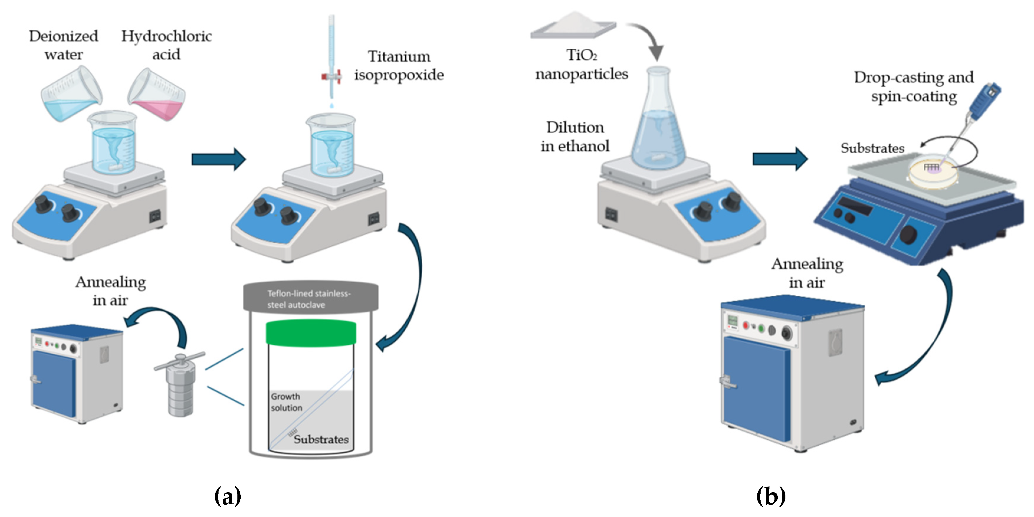
Figure 2.
Schematic representations of (a) and (b) perovskite solar cells having mesoporous (m-TiO2) and nanorods (TiO2-NRs) as ETLs, respectively and (c) and (d) the m-TiO2/s-TiO2/FTO/glass and TiO2-NRs/s-TiO2/FTO/glass heterostructures used for photocatalysis, respectively. Thicknesses are not in scale.
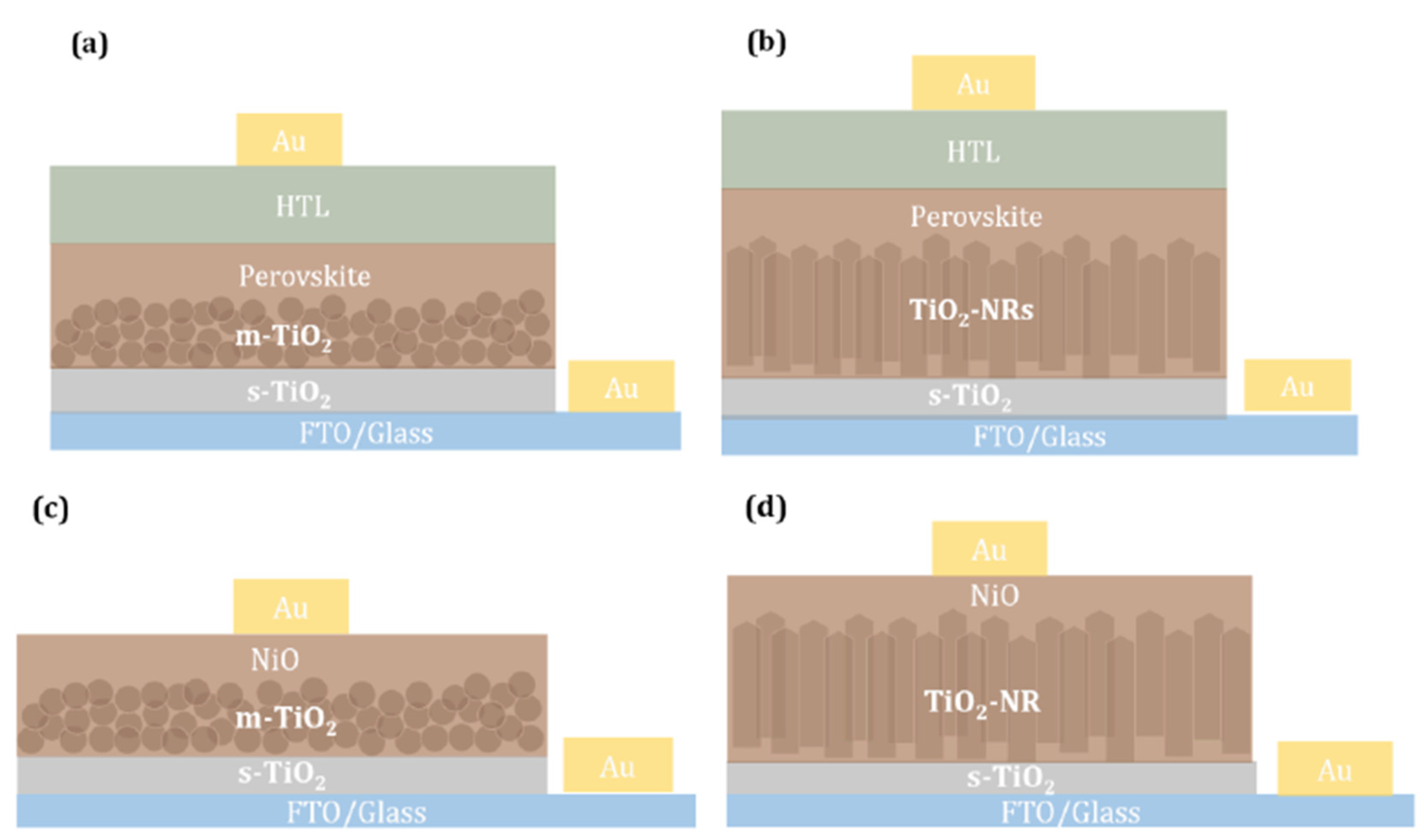
Figure 3.
(a) AFM surface image and (b) XRD pattern of m-TiO2 grown by spin coating on s-TiO2/FTO/glass substrates. The XRD pattern of FTO/glass is also shown.
Figure 3.
(a) AFM surface image and (b) XRD pattern of m-TiO2 grown by spin coating on s-TiO2/FTO/glass substrates. The XRD pattern of FTO/glass is also shown.
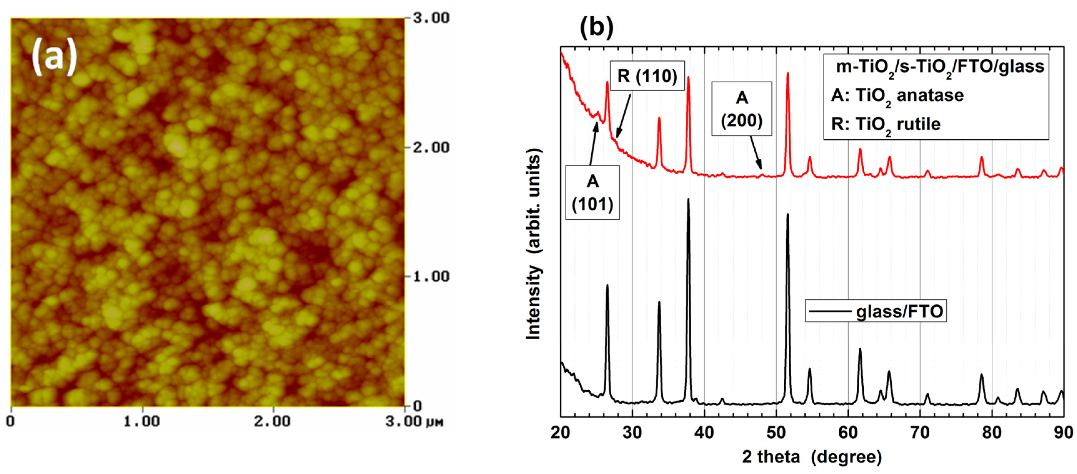
Figure 4.
SEM images of TiO2-NRs grown after (a) 40 min, (b) 60 min and (c) 80 min by a hydrothermal technique.
Figure 4.
SEM images of TiO2-NRs grown after (a) 40 min, (b) 60 min and (c) 80 min by a hydrothermal technique.
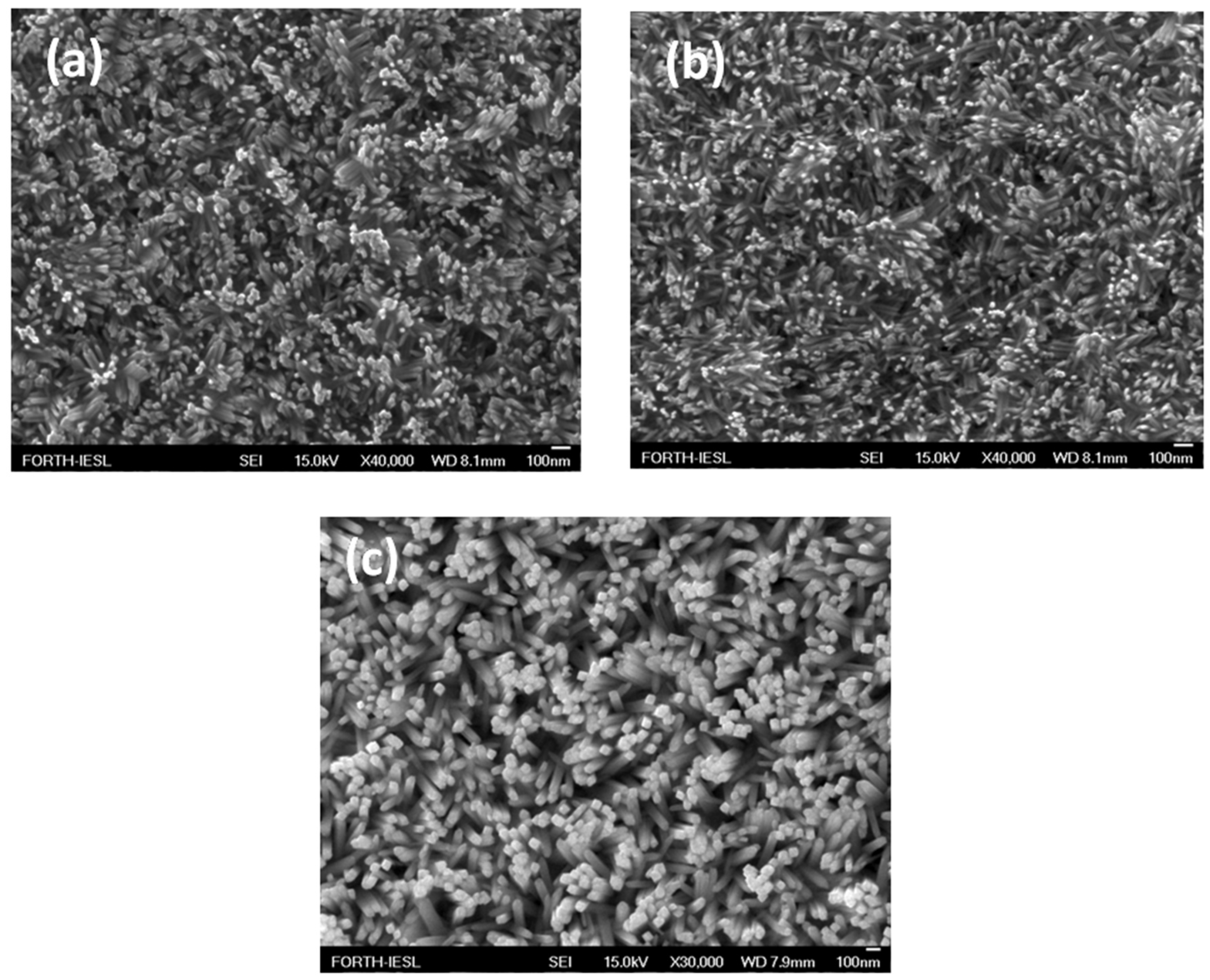
Figure 6.
Cross-sectional SEM images of PSCs having as ETL (a) m-TiO2 and (b), (c) TiO2-NRs with 300 nm (ETL1) and 600 nm (ETL2) tall NRs, respectively.
Figure 6.
Cross-sectional SEM images of PSCs having as ETL (a) m-TiO2 and (b), (c) TiO2-NRs with 300 nm (ETL1) and 600 nm (ETL2) tall NRs, respectively.
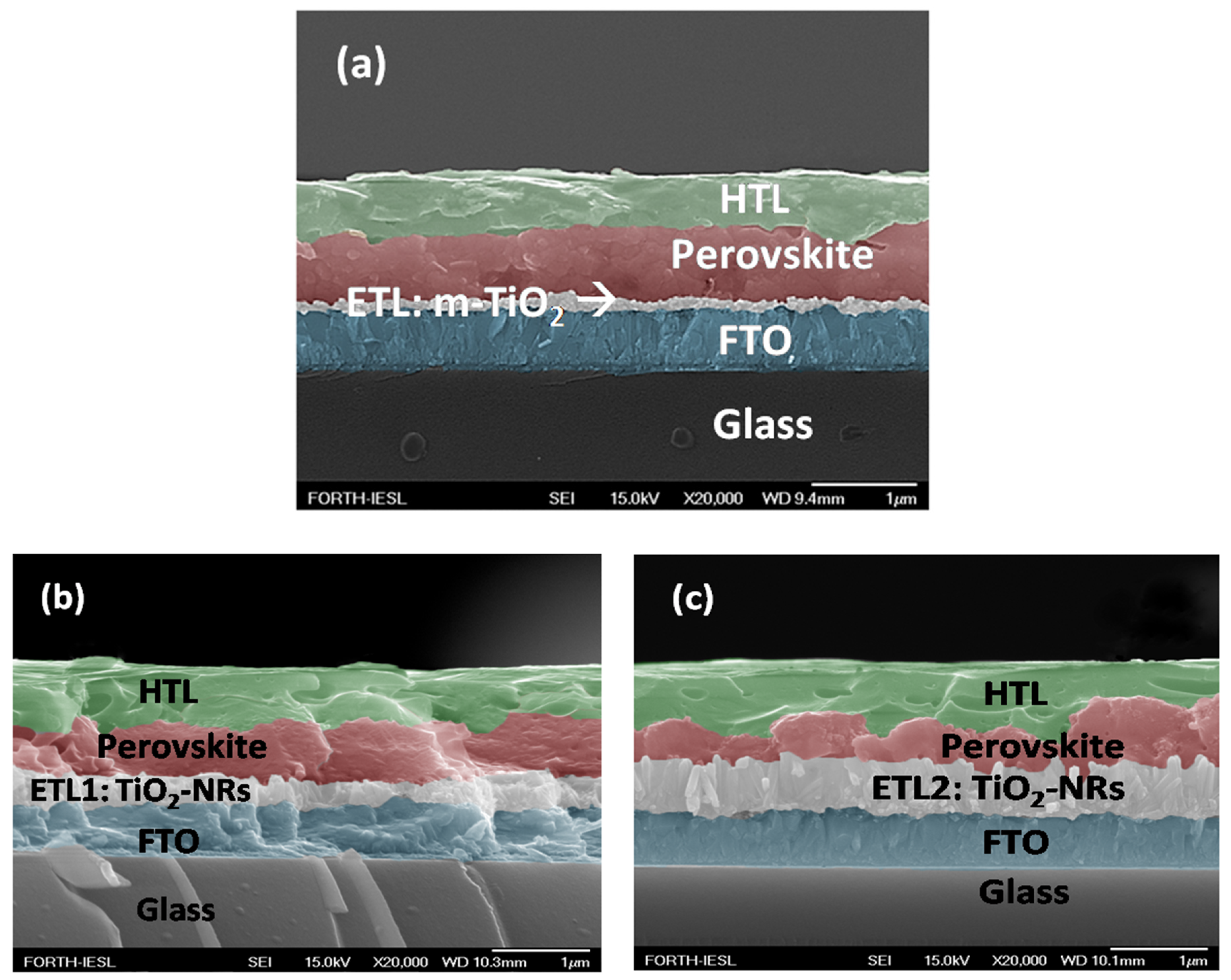
Figure 7.
(a) Dark current density – voltage (Id-V) characteristics and (b) photo-current density – voltage characteristics (Iph-V) under AM1.5 illumination of 3-D PSC and 1-D PSC1 and 1-D PSC2.
Figure 7.
(a) Dark current density – voltage (Id-V) characteristics and (b) photo-current density – voltage characteristics (Iph-V) under AM1.5 illumination of 3-D PSC and 1-D PSC1 and 1-D PSC2.
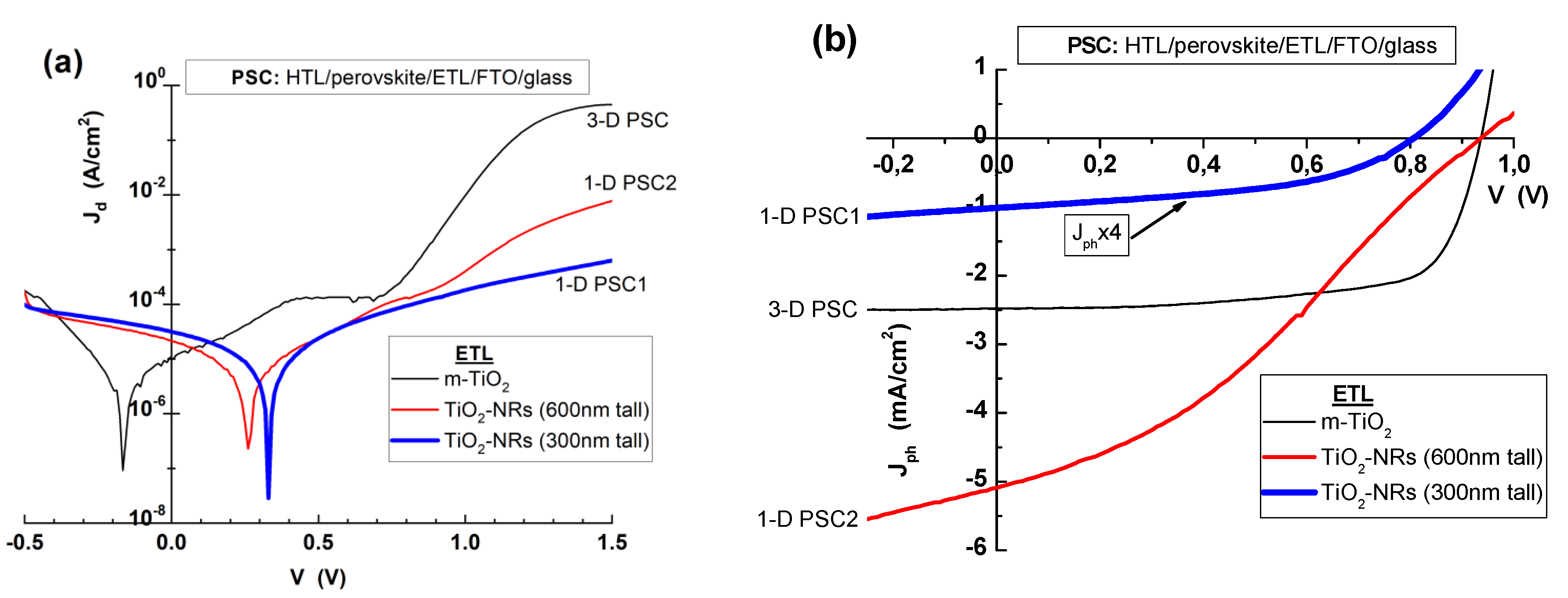
Figure 8.
Wide-scan XPS spectra of undoped NiO and doubled-doped NiO:(Nb,N) along with the spectra of the zoom-in circled area.
Figure 8.
Wide-scan XPS spectra of undoped NiO and doubled-doped NiO:(Nb,N) along with the spectra of the zoom-in circled area.
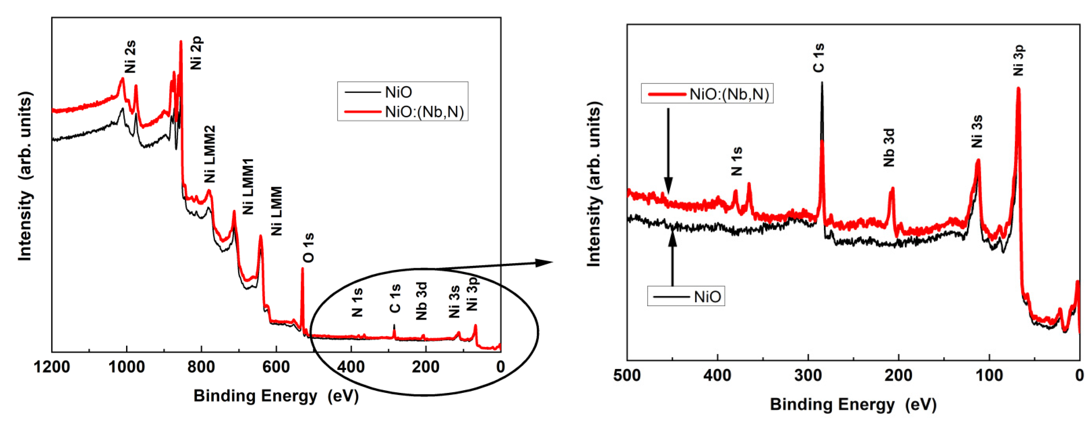
Figure 9.
SEM top view images of TiO2-NRs (a), NiO/TiO2-NRs (a1), m-TiO2 (b) and NiO/m-TiO2 (b1). Tilted 30o view images of NiO/TiO2-NRs (a2) and NiO/m-TiO2 (b2).
Figure 9.
SEM top view images of TiO2-NRs (a), NiO/TiO2-NRs (a1), m-TiO2 (b) and NiO/m-TiO2 (b1). Tilted 30o view images of NiO/TiO2-NRs (a2) and NiO/m-TiO2 (b2).
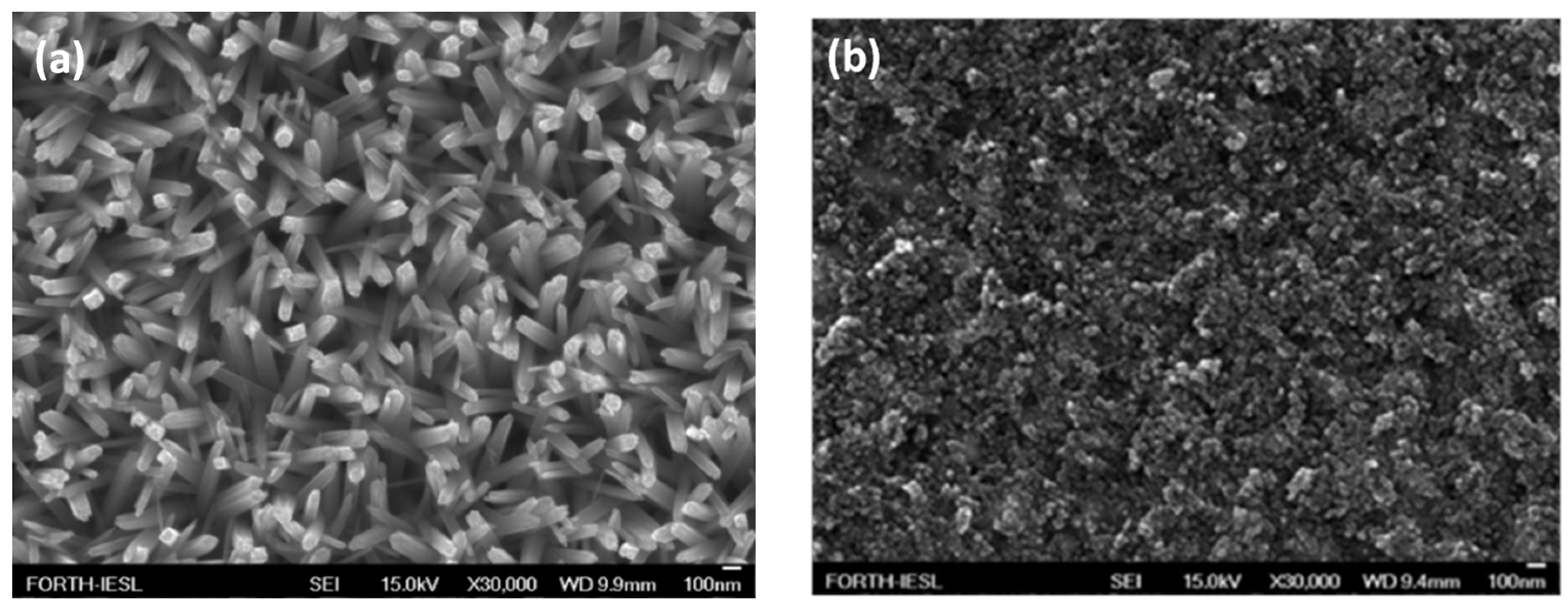
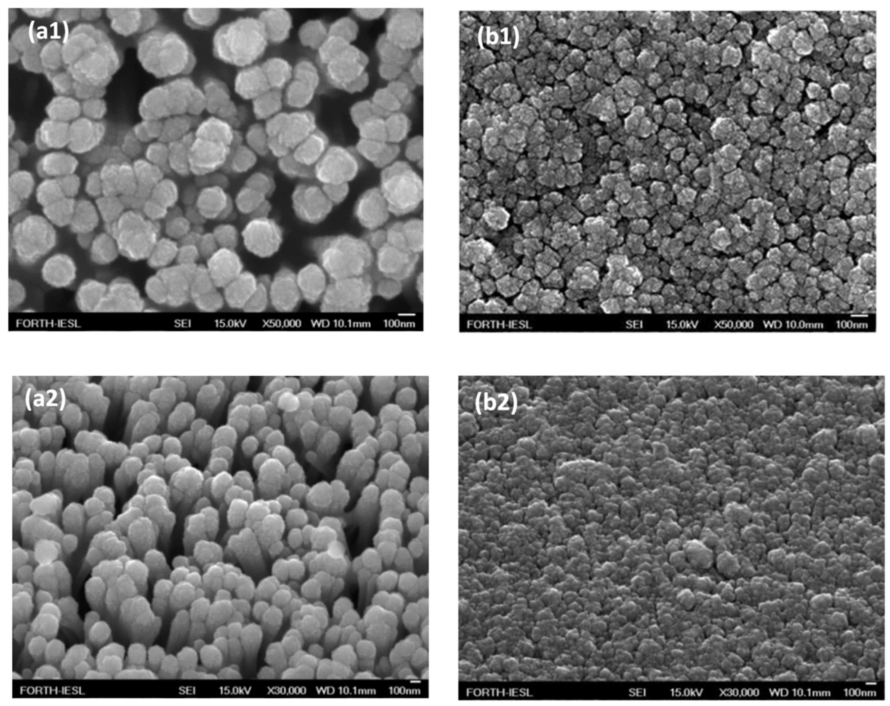
Figure 10.
Dark current density – voltage curves of 1-D and 3-D NiO/TiO2 heterostructures.
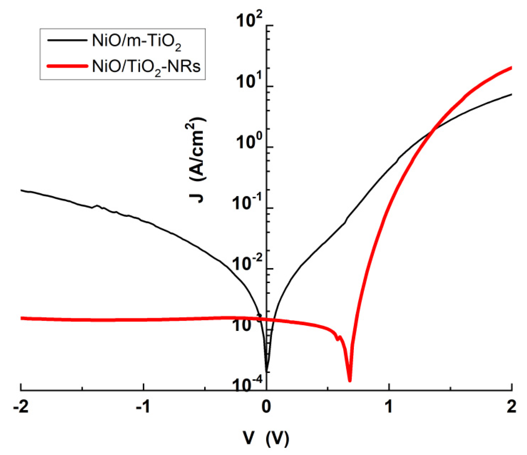
Figure 11.
Methylene Blue decolorization over time under UV light irradiation of 1-D (NiO/TiO2-NRs) and 3-D (NiO/m-TiO2) structures. The blue curve refers to the diode with TiO2 NRs, while the red curve to that with the m-TiO2.
Figure 11.
Methylene Blue decolorization over time under UV light irradiation of 1-D (NiO/TiO2-NRs) and 3-D (NiO/m-TiO2) structures. The blue curve refers to the diode with TiO2 NRs, while the red curve to that with the m-TiO2.
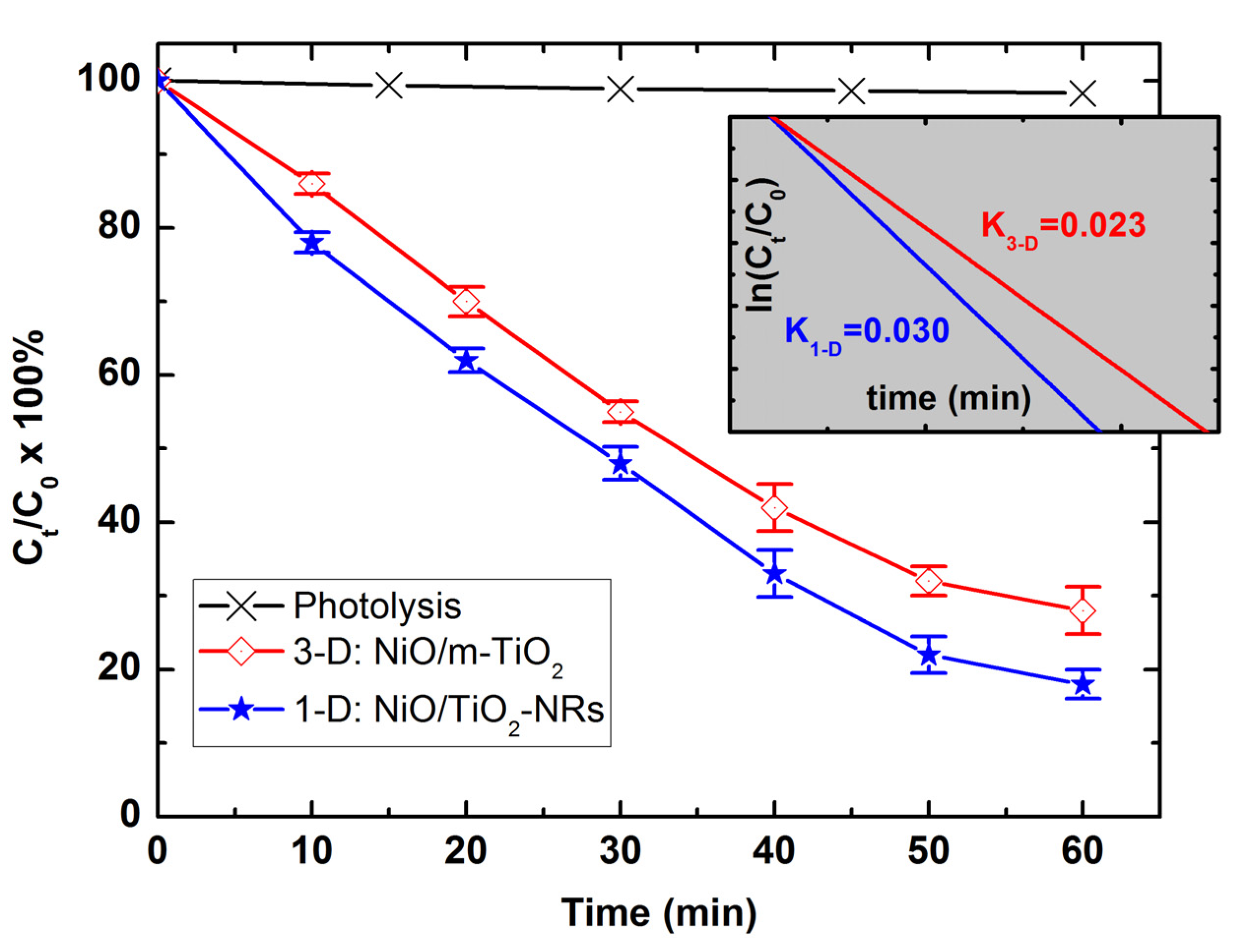

Table 1.
Diode parameters of 3D and 1-D PSCs in the dark (Id-V) and PSC parameters under AM1.5 illumination (Iph-V). RS is the series resistance, n is the ideality factor, JSC is the short-circuit current density, VOC is the open-circuit voltage, FF is the fill factor and η is the conversion efficiency.
|
PSC (ETL) |
Jd-V analysis | Jph-V analysis | ||||
| RS (kΩ) |
n | JSC (mA/cm2) | VOC (mV) |
FF | η (%) |
|
| 3-D PSC (m-TiO2) | 0.16 | 2.31 | 2.47 | 936 | 70.5 | 1.63 |
| 1-D PSC1 (TiO2-NRs 300 nm) | 45.16 | 11.67 | 0.26 | 805 | 45.4 | 0.09 |
| 1-D PSC2 (TiO2-NRs 600 nm) | 3.25 | 4.84 | 5.10 | 936 | 33.1 | 1.58 |
Table 2.
NiO and NiO:(Nb,N) properties as-prepared and after TT1. D is the crystal size, εL is the lattice strain, EU is the Urbach tail states width and ρ is the resistivity.
Table 2.
NiO and NiO:(Nb,N) properties as-prepared and after TT1. D is the crystal size, εL is the lattice strain, EU is the Urbach tail states width and ρ is the resistivity.
| NiO Samples |
Treatment | roughness (nm) | 2θ (degree) | D (nm) | εL (x10-2) |
Direct Egap (eV) | ρ (Ωcm) |
| undoped NiO |
As-prepared | 2.87 | 42.56 | 5.33 | 1.77 | 3.28 | 1.4x10⁻¹ |
| TT1 | - | 43.40 | 7.44 | 1.24 | 3.67 | 1.6x10³ | |
| double-doped NiO:(Nb,N) |
As-prepared | 2.75 | 42.66 | 10.07 | 0.94 | 3.71 | 6.9x10³ |
| TT1 | 43.04 | 9.13 | 1.02 | 3.74 | - |
Table 3.
Diode parameters of 1-D and 3-D NiO/TiO2 heterostructures. JS is the dark current density, RS is the series resistance, n is the ideality factor and φb is the barrier height.
Table 3.
Diode parameters of 1-D and 3-D NiO/TiO2 heterostructures. JS is the dark current density, RS is the series resistance, n is the ideality factor and φb is the barrier height.
| Heterostructure | JS (A/cm2) |
RS (Ω) |
n | φb (eV) |
| NiO/m-TiO2 | 2x10⁻³ | 8.20 | 6.96 | 0.58 |
| NiO/TiO2-NRs | 2x10⁻⁸ | 2.90 | 2.50 | 0.87 |
Disclaimer/Publisher’s Note: The statements, opinions and data contained in all publications are solely those of the individual author(s) and contributor(s) and not of MDPI and/or the editor(s). MDPI and/or the editor(s) disclaim responsibility for any injury to people or property resulting from any ideas, methods, instructions or products referred to in the content. |
© 2025 by the authors. Licensee MDPI, Basel, Switzerland. This article is an open access article distributed under the terms and conditions of the Creative Commons Attribution (CC BY) license (http://creativecommons.org/licenses/by/4.0/).
Copyright: This open access article is published under a Creative Commons CC BY 4.0 license, which permit the free download, distribution, and reuse, provided that the author and preprint are cited in any reuse.


