
Submitted:
12 November 2024
Posted:
13 November 2024
You are already at the latest version
Abstract
Doping engineering has been applied in niobium-doped NiO (NiO:Nb) by adding nitrogen (N) in its structure. The rf-sputtered films were made from a Ni-Nb composite target on unheated substrates at 300 W rf power and 5 mTorr total pressure. The plasma contained 50% Ar and 50% O2 for the fabrication of the single-doped NiO:Nb film (AΝ film), and N2 gas for the incorporation of N in the Ni-O-Nb structure. The N2 in plasma was introduced by keeping constant the flow rates of O2 and N2 gases (O2/N2=1) and reducing the amount of Ar gas, namely 94% Ar, 3% O2, 3% N2 (film AN1), 50% Ar, 25% O2, 25% N2 (film AN2), 6% Ar, 47% O2, 47% N2 (film AN3). All films had the single phase of cubic NiO and both Nb and N in the Ni-O structure were revealed by XPS experiments. The roughness of the films was increased with the increase of N in plasma. Post-deposition thermal treatment improved the crystallinity and reduced the structural disorder of the films. The AN2 film was found to be the most transparent of all films exhibiting the widest band gap, 3.72 eV, and the narrowest Urbach tail states width, 313 meV. The AN and the AN2 films were employed to form NiO/TiO2 heterostructures. The NiO:Nb/TiO2 and NiO:(Nb,N)/TiO2 heterostructures exhibited a visible transmittance of around 42% and 75%, respectively and both showed rectification properties. Upon illumination with UV light, the NiO:(Nb,N)/TiO2 diode exhibited enhanced photovoltaic performance when compared to the NiO:Nb/TiO2 solar cell: the short circuit current densities were 0.2 mA/cm2 versus 1.4 μA/cm2 and the open-circuit voltages were 0.5 V versus 0.2 V. The output characteristics of the p-NiO:(Nb,N)/n-TiO2 UV-photovoltaic can be further improved by proper engineering of the individual layers and device processing procedures.
Keywords:
NiO
; co-doping
; NiO:Nb
; NiO:(Nb
; N)
; ultraviolet photovoltaic
; NiO/TiO2 heterojunction
; Urbach tail
; sputtering
; TiO2
; optical properties
1. Introduction
It has been realized beyond any doubt that the climate change we are experiencing requires a complete decarbonization of the energy system towards a net-zero energy future. The building sector (residential, offices and commercial buildings), when compared to the transportation and industrial sectors, consumes more than 45% of the primary energy used in Europe and is responsible for 36% of greenhouse gases [1]. From the whole building envelope, the windows are responsible for the building’s energy losses thus necessitating the consumption of large amounts of energy to maintain indoor temperature and the well-being of the inhabitants. Even though the smart windows, which first appeared almost 40 years ago [2] as a promising energy-saving technology for controlling the solar spectrum (heat and lighting), the lack of fully dynamic and end-user control of their functionalities hampered their wide commercialization. Over the last decade with the huge advance in the science and technology of materials, there has been a considerable effort in overcoming these problems by developing the next generation of smart windows for climate neutral buildings, which exploit the solar spectrum by simultaneously producing, manipulating and storing the solar energy without losing any of its properties as “windows”. Thus, there have already been reports on smart windows having thermochromic or dual band electrochromic coatings for controlling the solar spectrum along with transparent photovoltaics producing electricity and microcapacitors for storing energy on a single window [3,4,5,6,7]. The transparent solar cells required for the next generation smart windows utilize only around 7% of the solar spectrum which accounts for the ultraviolet (UV) part of it. The theoretical efficiency of transparent photovoltaics (PV) has been estimated to be 21% [8]. Wide band gap oxide-based semiconductors, with high visible transmittance, can be used for forming the required p-n junction and thus fabricating transparent PVs absorbing the ultraviolet radiation.
Nickel oxide (NiO) is a p-type oxide semiconductor and its conductivity is due to non-stoichiometric defects such as Ni vacancies and oxygen interstitials. Because of its hole conductivity, high chemical stability and combined with wide band gap energy (3.1-3.8 eV), it is the most widely used p-type transparent conductive oxide. Furthermore, NiO has attracted attention because its properties can be modified by doping engineering depending on applications such as sensing, microbatteries, photocatalysis, etc. Single or double doping of NiO has been reported mainly by cation dopants like Li, Nb, Fe, Cu, Zn, Mg, Al, Co, Pb, Ir, etc, whereas tuning its magnetic, optical and electrical properties has been attempted by cation and anion co-doping. In particular, the use of nitrogen (group-V element) as anion dopant in Cu-doped NiO has been shown to deteriorate its electrical properties but increase its optical transmittance [9]. Furthermore, doping of NiO with niobium (NiO:Nb) has been shown that, apart from improving its photocatalytic and sensing properties, it improves its linear and nonlinear optical properties for potential nanophotonic applications [10], whereas when combined with TiO2 the formed heterodiode can reveal photovoltaic behaviour, albeit with poor output characteristics [11].
In this work, nitrogen was incorporated as anion dopant into the structure of sputtered NiO:Nb films and the effect of double doping with varying amounts of nitrogen (N) on the properties of the films was investigated in an attempt to enhance the photovoltaic performance of NiO:Nb based solar cells. It is revealed that the NiO:(Nb,N) with the optimum amount of anion dopant can remarkably enhance the output ultraviolet photovoltaic characteristics of the NiO:(Nb,N)/TiO2 heterostructure when compared to the NiO:Nb/TiO2 one: increase of short-circuit current by two orders of magnitude and increase of open-circuit voltage by a factor of 2.5. The output characteristics of the p-NiO:(Nb,N)/n-TiO2 UV-photovoltaic can be further improved by proper engineering of the individual layers and device processing procedures. These results pave the way for the double-doped NiO:(Nb,N) to be used in all-oxide transparent photovoltaics on next generation smart windows for energy efficient buildings.
2. Materials and Methods
2.1. Thin Films and Devices: Fabrication and Characterization
The NiO thin films were deposited by radio frequency (rf) sputtering from a Ni-Nb composite target on room temperature substrates (patterned glass and Si pieces—see below for substrates’ details). The composite target was a Ni target (6 in. diameter, purity 99.99%) on top of which 14 Nb pellets (dia. 1.5cm x 3mm thick, 99.95% purity) were placed [11]. The sputtering plasma consisted of a mixture of Ar-O2 gases for the fabrication of the reference single-doped Nb-doped NiO films (NiO:Nb), whereas N2 gas was added in the plasma for depositing the double-doped NiO:(Nb,N) films by keeping the ratio of O2 and N2 flow rates equal to one, O2/N2=1. Mass flow controllers were used to adjust the flows of the three gases (Ar, O2 and N2) to keep the ratio O2/N2=1 by appropriately modifying the flow rate of Ar and keeping the total pressure constant at 0.67 Pa (5mTorr). The substrate holder was 10 cm above the target and the latter was powered by 300 W. Target conditioning was performed by pre-cleaning in Ar plasma at 0.67 Pa (5mTorr) and 300 W for 45 minutes before each deposition run. Before immersing the Si substrates into the sputtering chamber, they were treated for 15 minutes in an ultrasonic bath containing organic solvents, then cleaned in alcohol and deionized water and purged in dry Nitrogen. This was followed by an additional dip in 10% HF solution to remove the native oxide from its surface before inserting it in the deposition chamber. Whenever an insulating and or transparent substrate was required for specific characterization techniques of the sputtered NiO-based films, an 1 inch x 1 inch glass substrate was used having all the required geometrical patterns. The patterns were made by using a specially designed two-level photolithography mask and standard optical lithography techniques. Details on the deposition parameters/conditions of the films have been tabulated in Table 1. Τhe thickness was measured by a Veeco Dektak 150 profilometer and the films were thermally treated ex-situ after deposition at 300 oC in flowing N2 gas for 15 minutes (TT1). The optimum NiO:(Nb,N) film, with regards to its properties, was chosen to be deposited on a TiO2/FTO/glass substrate and form the heterostructure. The TiO2 layer was a bi-layer formed by spin-coating a 200 nm thick mesoporous TiO2 on top of a 40 nm thick compact TiO2 layer. Each of these TiO2 layers had been heated in air at 500 oC. The TiO2 layer was the one used as electron transfer layer in perovskite solar cells and details about the formation conditions and properties of the TiO2/FTO/glass can be found elsewhere [12].
The surface morphology of the films was examined by Field-Emission Scanning Electron Microscopy (FE-SEM) employing the Jeol JSM-7000F electron microscope, which was equipped with an Energy-Dispersive X-ray (EDX) spectroscopy system (Oxford Instrument-INCA) for elemental analysis on the films. The existence of the dopants (Nb and N) in NiO was confirmed by EDX for the Nb dopant and X-ray Photoelectron Spectroscopy (XPS) for both the N and Nb dopants on selected NiO films. The XPS experiment was carried out on a Specs Lab photoelectron spectrometer, with a base pressure in the analysis chamber of 1.33x10⁻⁷ Pa. The X-ray source was the Al Kα radiation (1486.6 eV, monochromatized) at 13 kV and a power of 200 W. In order to take into account the charging effect on the measured binding energies the spectra were calibrated using the C1s line (BE = 284.8 eV) of the adsorbed hydrocarbon on the sample surface. The XPS spectra were recorded by collecting binding energies from 0 to 1100 eV for the wide scan survey spectra. Before the XPS measurements, the samples were ex-situ heated to 100 oC for 5 min and their surface was in-situ etched for 10 min by 0.75 keV Ar+ with a current density of around 5 mA/cm2 to remove any adsorbed contaminants which could originate from transferring the sample in ambient conditions.
Atomic force microscopy (AFM) measurements were performed to determine the Root Mean Square (RMS) roughness of the films’ surface. The AFM measurements were carried out in tapping mode, with the Digital Instruments-Multimode system, using sharp tips (8 nm tip radius; Si material, PPP-NCHR type from NanosensorsTM).
The structure of the NiO films was studied by the X-Ray Diffraction (XRD) method. The measurements were performed using a Rigaku D-max 2000 system, with Cu Kα1 radiation (λ=1.5406Å) and a fixed power source (40 kV and 30 mA). The diffractometer was set in the condition of grazing incident Xray diffraction (GIXRD) with ω = 1.6 o at a rate of 0.02°/sec and the 2-theta angle over the range of 30-90°. The average crystallite size and lattice strain were estimated from the Scherrer formula:
and the formula:
respectively, where k is the shape factor 0.94, λ is the wavelength of incident radiation 1.5406 Å, hkl represents the Muller indices of the diffraction plane, βhkl is the full width at half maximum, and θ is the Bragg angle of the peak [13].
D = kλ/βhklcosθ
εL = βhklcotθ/4
The basic optical properties of the NiO films were determined through the Tauc plots after monitoring the normal incidence transmittance in the UV-Vis-NIR spectrum by employing a Perkin Elmer Lambda 950 system. The optical direct band gap and the Urbach tails width of the films were extracted through the relationships
and
and plotting [(αhv)2-vs-hv] and lnα-vs-hv, respectively [14,15]. In the above equations: T is the transmittance, which was corrected for the transmittance of the substrate, d is the thickness, α is the absorption coefficient, h is the Planck constant, v is the frequency, E is the photon energy, C is a constant and EU is the Urbach energy.
T~exp(-αd)
α = Cexp(E/EU)
The resistivity of the NiO-based films was determined by employing the conventional four-probe Van der Pauw technique on films deposited on glass substrate having stripes, 800 μm long and 250 μm wide and square pads with Au ohmic contacts (400 μm x 400 μm and 150 nm thick) deposited by electron beam evaporation. The quality of the Au metal as ohmic contact on the NiO-based films of this investigation was tested by employing the linear transmission line measurements (l-TLM) technique [16,17,18] for films deposited on glass. Square Au pads having increasing distance, L, between each other were deposited on stripes of NiO-based films. By plotting the measured resistivity, R, between pads as a function of L a straight line was obtained from which the specific contact resistance between the Au metal and the film could be obtained. A typical example is seen in Figure 1a for the AN3 film (NiO:(Nb,N). It was found that the specific contact resistance of Au on the NiO:Nb was 0.2 Ωcm2 and increased by one order of magnitude for the NiO:(Nb,N) film (2.6 Ωcm2). It should be reminded that the optimum ohmic contact on semiconductors should exhibit a specific contact resistance as low as 10-3-10-4 Ωcm2 [17,18]. Whenever p-NiO has been used in optoelectronic devices, Au [19,20,21], Ni/Au [22], Ag [23,24,25,26], Al [27] and Pt [28,29] have been reported as ohmic contact metals on p-NiO. No attempt was made to improve the ohmic contact behaviour on p-NiO since it was beyond the scope of this investigation. The NiO:Nb/TiO2 and NiO:(Nb,N)/TiO2 heterostructures were fabricated by placing the TiO2/FTO/glass substrates in the sputtering chamber and the depositions of the NiO:Nb and the optimum NiO:(Nb,N) thin films were made using the sputtering conditions described in Table 1. As ohmic contacts, sputtered Au metal was used for both the NiO-based and the FTO layers, using a specially designed shadow mask which defined the junction area of the diode (7.8x10⁻³ cm2). A schematic representation of the fabricated NiO:Nb/TiO2 and NiO:(Nb,N)/TiO2 heterodiodes can be seen in Figure 1b. The diodes were characterized just after fabrication and after thermal treatment TT1 (300oC, N2, 15 min.
The dark current–voltage (I–V) characteristics of the heterodiodes were recorded using the Agilent 4200-SCS unit from which the diodes’ parameters were extracted following thermionic emission theory from the I-V curves [30,31]. The photo I-V characterization was performed by illuminating the diodes from the back side (glass substrate) with a He-Cd cw laser at 325 nm laser having an intensity of 0.71 W/cm2. The I-V curves under illumination were recorded by employing the Keithley 2401 SMU instrument.
3. Results
3.1. Thin Films Properties
3.1.1. Properties of TiO2 Layer
The TiO2 layer, which was used for the fabrication of the NiO-based/TiO2 heterostructures, was made by the spin coating technique, as described in subsection 2.1. The TiO2 structure consisted of a mixture of anatase and rutile phases, whereas the RMS roughness of the surface was 20 nm. The visible transmittance of the TiO2/FTO/glass was 75-85%. A full account of the properties of the TiO2 layer can be found in Ref. [12].
3.1.2. Properties of NiO:(LNb,N) Thin Films
It has been shown in a previous investigation [11] that the undoped NiO films fabricated from a Ni target at 300 W in plasma containing 50% Ar and 50% O2 gases in total pressure of 0.67 P (5 mTorr) are O-rich, p-type materials with high structural disorder and low visible transmittance. By adding Nb as dopant in NiO it was shown [10,11] that Nb replaces Ni atoms and the resulting single-doped NiO:Nb retains the p-type conductivity and the low transmittance of undoped NiO but improves its conductivity. On the contrary, doping NiO with nitrogen (N) resulted in single doped NiO:N films with the opposite properties to those of NiO:Nb, namely low conductivity, high visible transmittance and much lower structural disorder [31]
In order to investigate the effect of introducing N in the structure of Nb-doped NiO, the Ar flow was reduced in the plasma during deposition and at the same time N2 gas was introduced in the sputtering chamber by keeping the ratio of flow rates constant, O2:N2=1 and the total pressure at 5 mTorr (0.67 P). By doing so, the amount of the heavy atoms of Ar gas in plasma was reduced, as seen in Table 1, thus leading to reduced deposition rate for the fabricated films: from 1.59 nm/min for the film made in N-free plasma (Ar:O2:N2 = 50:50:0, AN film) to 1.30 nm/min for the film made in 47% N2 containing plasma (Ar:O2:N2 = 6:47:47, AN3 film). The reduction of heavy Ar species in plasma was accompanied by the reduction of Nb atoms in the grown film. As deduced by EDX measurements and presented in Table 1, the atomic percentage (at.%) of Nb in Ni-O structure was reduced from 3.5 to 1.4. However, the unambiguous incorporation of the light N atom in the Ni-O-Nb structure could only be revealed by XPS experiments. The XPS experiment was selectively performed on the double-doped AN2 film (Ar:O2:N2=50:25:25) and the N-free single-doped NiO:Nb –AN film (Ar:O2:N2 = 50:50:0) and the results have been plotted in Figure 2. The wide-scan spectra are plotted in Figure 2a where the characteristic peaks of Ni, O as well as those of the dopants, N and Nb, can be clearly observed. The latter peaks, N and Nb, have been expanded and shown in Figures 2b and 2c, respectively. The features of Nb peak at around 209 eV and 207 eV, seen in Figure 2b, correspond to Nb 3d3/2 and Nb 3d5/2 indicating that Nb exists in Ni-O structure and is fully oxidized into its maximum valence of +5 (Nb5+) [11,32,33].
The effect of introducing N in the Nb-doped Ni-O structure on the structural and optical properties of the films just after deposition was examined by XRD measurements and monitoring the UV-Vis-NIR transmittance. The XRD patterns of the as-prepared double-doped AN1, AN2 and AN3 films, along with those of the single doped NiO:Nb -AN film and the crystal NiO (Joint Committee of Powder Diffraction Standards (JCPDS) card No: 04-0835) are shown in Figure 3a. As can be seen, there is one main diffraction peak at around 42.6o and two more peaks with much lower intensity at around 36.5o and 62.2o. All diffraction peaks were identified as those arising from the (200), (111) and (220) crystallographic planes, respectively, of the cubic NiO phase. Niobium oxide or any nitride phases could not be detected. The asterisks in Figure 3a denote diffraction peaks originating from the films’ Au metallization pads which had been applied for performing the electrical characterization of the films (JCPDS card no 040-0784). The crystallographic parameters which were extracted from the XRD patterns, like average crystallite size and lattice strain, have been tabulated in Table 2.
It is seen that upon N-doping of NiO:Nb and when compared with the single-doped NiO:Nb AN-film: (i) there is a small shift to higher angles, as clearly seen for the highest (200) diffraction peak, indicating compressive stress, (ii) the average crystallite size increased by almost 90%, from 4.7 nm for the AN film to 8.9 nm for the AN2 film and (iii) the strain reduces by around 50%, from 17.8x10⁻³ to 9.15x10⁻³. Taking into account that the (200) diffraction peak of crystal NiO appears at 43.3o, Nb doping has created tensile stress in the Ni-O structure despite the relatively smaller ionic radius of Nb5+ (0.64 Å) than that of Ni2+ (0.69 Å) [34,35]. As in the case of N-doped NiO, where the N in NiO reduces the strain of Ni-O structure [21], the introduction of N as second dopant in Ni-O-Nb structure relaxed the tensile stress reducing the lattice stress. The co-doping of NiO:Nb film with nitrogen increased the surface porosity and the RMS roughness of the films along with the increase in crystallite size. This can be seen in Figure 4, where the SEM and AFM images of the N-doped NiO:Nb films are shown. The respective images of the reference single-doped NiO:Nb AN-film are not shown since surface topography and roughness (Table 2) were similar to those of AN1 film.
The structural improvement concerning crystallite size and stress of NiO:Nb films upon doping with N, was reflected in the optical properties of the double-doped NiO:(Nb,N) films. Figure 3b shows the transmittance of the as-prepared films and it is seen that N co-doping of NiO:Nb films increased transmittance particularly for the AN2 film. The enhanced transmittance of the N-doped NiO:Nb films was accompanied by an increase in the energy band gap (Egap) and a decrease of the tail states width (Urbach energy, EU). The direct Egap and the EU values of the films have been tabulated in Table 2, along with the structural properties. It is seen that the introduction of N in NiO:Nb films increased the direct band gap and reduced the structural disorder by reducing the band gap states and the localized states near the valence band edge (EU). The biggest optical direct band gap and the narrowest tail states width were observed for the AN2 film which was deposited in plasma containing 50% Ar, 25% O2 and 25% N2 gases. Since the aim of this investigation was to fabricate solar blind and transparent solar cells based on all-oxide NiO/TiO2 heterostructures, in the following we proceeded only with the most transparent double-doped NiO:(Nb,N) fabricated in this work, namely the AN2 film and compared it with the reference single-doped AN film (NiO:Nb).
Before fabricating the NiO/TiO2 heterostructure the AN and AN2 films were annealed and their structural and optical properties after thermal treatment TT1 are depicted in Figure 5a and 5b, respectively, whereas the respective properties extracted from these plots have been tabulated in Table 3. The general improvement of films’ crystallinity after TT1 when compared with that of the as-prepared films seen in Figure 3 and Table 2 is explicit. In addition, the AN2 film showed superior properties after TT1 than those of AN film: increased crystallite size, less lattice stress, larger band gap and narrower width of tail states (Urbach width). These properties are expected to significantly affect the transport of the carriers by reducing their scattering at the grain’s or crystallite’s boundaries or trapping them into states which can act as recombination centers.
The resistance of the films was high enough to allow any reliable Hall measurements to be performed. The defective and disordered single-doped NiO:Nb had resistance, measured between the opposite contact pads of Hall pattern, of a few tens of kΩ. Upon co-doping with nitrogen, as shown above, the film exhibited an increase in resistance to a few hundreds of kΩ. This observation indicated that the increase in the energy band gap of NiO:(Nb,N) in this investigation is not associated with an increase in holes’ concentration due to the Moss-Burstein effect [36,37,38,39], according to which an increase in carrier concentration results in an increase in the energy band gap. The Moss-Burstein effect generally occurs in degenerated semiconductors, which is not the case of the investigated NiO-based films. The increase in films’ resistivity along with the observed reduction in structural disorder indicated that the NiO:(Nb,N) film has become more stoichiometric after the post-deposition heat treatment. Deterioration of the electrical properties and improvement of optical properties have been reported for NiOΝ films when doped with Cu [9]. It is the first time to our knowledge where the introduction of nitrogen as anion co-dopant in NiO:Nb films is reported to improve its optical transmittance, paving the way for applying NiO:(Nb,N) films in transparent optoelectronic applications. Nevertheless, more in-depth investigation is needed by theoretical calculations as well as experimental instrumentations so as to thoroughly explore and control the interaction mechanisms between Nb and N in the Ni-O structure.
3.2. NiO-Based Heterostructure Properties
The AN and AN2 films were employed to form the NiO/TiO2 heterostructures by depositing them by sputtering on the TiO2/FTO/glass substrates using the deposition conditions described in Table 1. The formation of the heterostructure was completed by heat treating the NiO/TiO2 films under TT1 conditions (300 oC, N2, 15 minutes) to improve the quality of the NiO films as shown in the previous sections. The NiO:Nb/TiO2 and the NiO:(Nb,N)/TiO2 films were tested for their transmittance and the dark current density—voltage (Jd-V) characteristics and the results have been plotted in Figure 6a and 6b, respectively. As seen in Figure 6a, where the transmittance of the TiO2/FTO/glass has also been plotted, the transmittance of the NiO:(Nb,N)/TiO2 heterostructure is larger than that of the NiO:Nb/TiO2 heterostructure. The enhancement in transmittance is due to the higher quality of the NiO:(Nb,N) –AN2 film than that of the NiO:Nb –AN film. The highly conductive FTO-covered glass substrate is responsible for the decrease in transmittance observed at long wavelengths for all films. Furthermore, as depicted in Figure 6b, both heterostructures show rectification behaviour but the NiO:(Nb,N)/TiO2 diode exhibited superior properties than the NiO:Nb/TiO2 diode. As seen in Table 4, where the diodes properties have been tabulated, the NiO:(Nb,N)/TiO2 diode has shown higher Jd(f)/ Jd(r) at ± 3 V, lower saturation current density (JS), higher series resistance (RS), larger barrier height (φb) and almost the same ideality factor (n) when compared to those of the NiO:Nb/TiO2 diode. The larger resistivity of the AN2 film than that of AN film is attributed to the high RS of the diode formed using the AN2 film. In addition, the better crystallinity and the less disordered structure of the AN2 film than that of AN film contributed as well to the better rectification properties for the respective heterostructures. The fact that the TiO2 layer was formed by spin-coating and not by sputtering as the doped NiO layers must be the reason for the high ideality factor. High values for the ideality factor have been observed in all-oxide diodes [40], oxides grown on epitaxial layers [21] or non-oxide epitaxially grown structures [41] and have been attributed to transport mechanisms through recombination at defects/states at the interface, tunneling through the interfacial layer or space charge current transport. However, the enhanced properties of the NiO:(Nb,N)/TiO2 diode in the dark is expected to show better output characteristics than the NiO:Nb/TiO2 diode upon illumination.
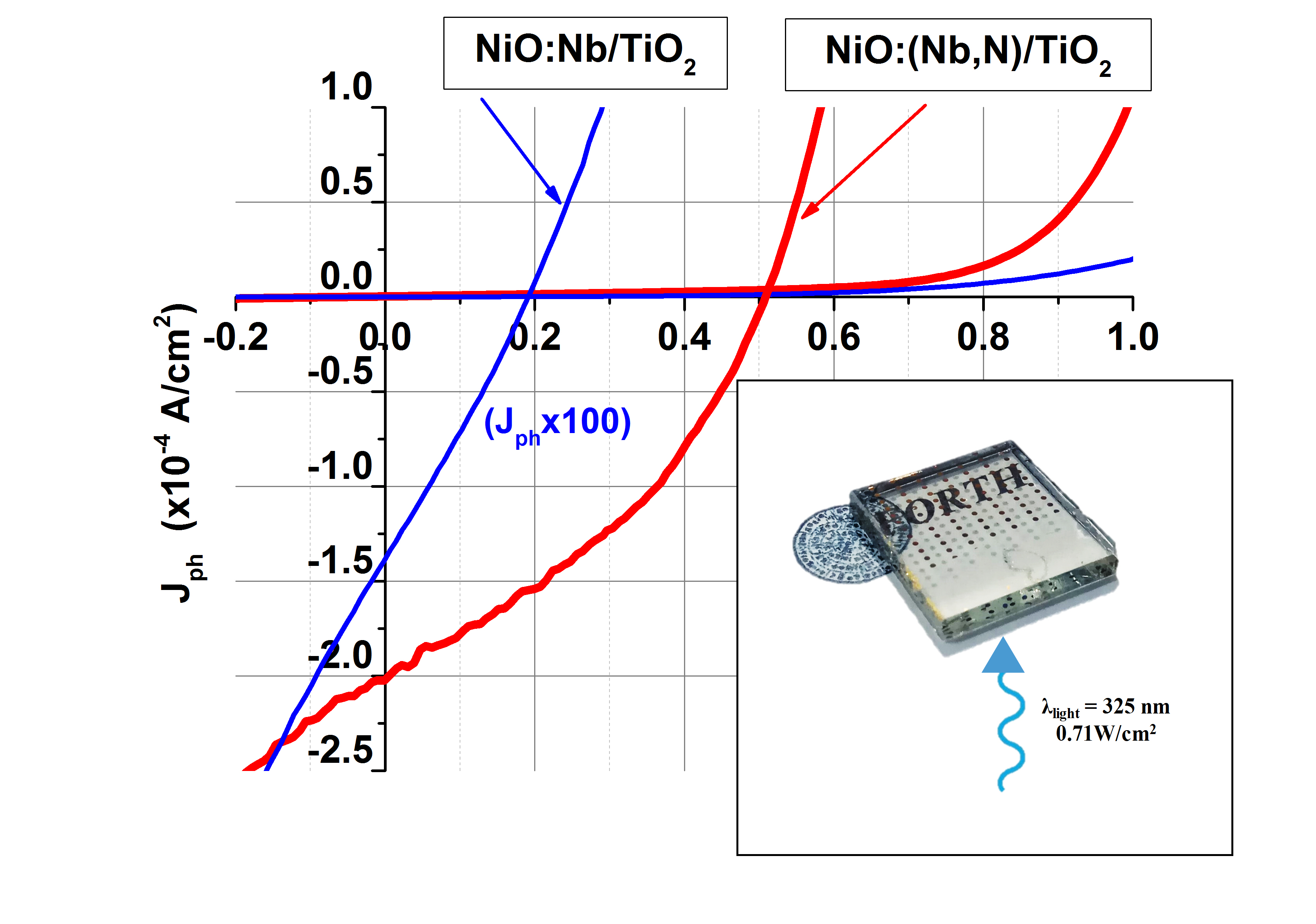
Figure 7 shows the current density—voltage characteristics of the NiO:Nb/TiO2 and the NiO:(Nb,N)/TiO2 heterodiodes after illumination with UV laser light of 325 nm wavelength from the glass substrate. Even though it is known that the NiO:Nb/TiO2 heterodiode can exhibit photovoltaic behaviour [11] photovoltaic activity was also observed for the NiO:(Nb,N)/TiO2 heterodiode. However, the photovoltaic characteristics of the NiO:(Nb,N)/TiO2 diode are far superior to those of the NiO:Nb/TiO2 one: the short-circuit current density (JSC) was 0.2 mA/cm2 and 1.4 μA/cm2, whereas the open-circuit voltage (VOC) was 0.5 V and 0.2 V, respectively. The enhancement of the output photovoltaic performance can be attributed to the double-doping of NiO, which affects the layers’ properties as well as the NiO-TiO2 interface by suppressing defects, modifying interface states and the depletion region, thus enhancing carrier transport and collection. Despite the relatively low photovoltaic efficiency of the diodes upon UV illumination, the double-doping of NiO has shown very enhanced UV photovoltaic performance when forming a p/n junction with TiO2. Theoretical calculations on Cu2O [42] have shown that double-doping can improve the properties of the material suggesting it can be a promising approach for developing more efficient oxide-based photovoltaic devices. This approach has been successfully applied for oxide-based PVs like dye-sensitized solar cells employing anion and cation co-doping of TiO2:(Al,N) [43] and double cation doping of BiFeO3:(Nd,Cr)-based solar cells [44] as well as non-oxide Cu2ZnSn(S,Se)4/CdS PVs (Li-Ag [45] and Co-Zn [46]). It is the first time, however, where a double-doped p-type NiO:(Nb,N) is employed in an all-oxide NiO/TiO2 UV-PV with enhanced photovoltaic properties are reported. The UV PV performance of the NiO:(Nb,N)/TiO2 heterojunction is very promising. It is expected that modifications concerning design and fabrication steps like the optimization of ohmic contact on NiO-based films, the elimination of the interface states by forming both NiO and TiO2 layers by sputtering, the intentional incorporation of an interlayer between the NiO-TiO2 interface and illumination of the device from the NiO side, will improve the performance of the diode in the dark and subsequently the behavior of the diode under illumination.
4. Conclusions
Nitrogen (N) was incorporated into the structure of Niobium-doped NiO (NiO:Nb) and the effect of double doping (Nb,N) on the properties of the NiO:Nb films was investigated to further enhance the photovoltaic performance of NiO:Nb based solar cells. The films were fabricated by the rf-sputtering technique by employing a Ni-Nb composite target and the depositions were made on room temperature substrates. The deposition power was kept at 300W and the total pressure was at 5mTorr. The plasma contained Ar, O2 and N2 gases and the content of N2 in plasma was introduced by keeping constant the flow rates of O2/N2=1, namely 94% Ar, 3% O2, 3% N2 (film AN1), 50% Ar, 25% O2, 25% N2 (film AN2), 6% Ar, 47% O2, 47% N2 (film AN3). A reference single-doped NiO:Nb film, AN0: 50% Ar and 50% O2 was also fabricated. Upon N co-doping, the O-rich NiO:Nb film became less disordered and more transparent. The structural disorder was further reduced and the transmittance was increased by post-deposition thermal treatment of the films at 300oC in N2 ambient. The AN2 film, which was fabricated in plasma containing 50% Ar, 25% O2, 25% N2, was the most transparent of other films fabricated in this work exhibiting the widest band gap and the narrowest Urbach tail states width. The direct band gap of the films, as well as the sub-gap states, the Urbach tail states, were correlated with the existence of the dopants in the Ni-O structure. The thermally treated AN2 film revealed a direct band gap of 3.72 eV and Urbach energy (tail states) width of 313 meV, which were 50 meV larger and 213 meV narrower when compared to the respective values of the NiO:Nb film. The heterojunction was formed on a TiO2 bi-layer, namely a spin-coated mesoporous TiO2 on top of a compact-TiO2, using FTO/glass as a substrate. The NiO:Nb/TiO2 and NiO:(Nb,N)/TiO2 heterostructures exhibited a visible transmittance of around 42% and 75%, respectively and both showed rectification properties. Upon illumination with UV light, the double-doped AN2 heterodiode revealed superior photovoltaic performance than that of single-doped AN0 heterodiode: short circuit current density of 0.2 mA/cm2 versus 1.4 μA/cm2 and an open-circuit voltage of 500 mV versus 200 mV, which is very promising for enhanced all-oxide transparent solar cells.
Author Contributions
Conceptualization, E.A.; methodology, E.A.; validation, C.A.; formal analysis, C.A.; investigation, C.A.; E.G.M., M.A., K.T., and C.K.; resources, E.G.M., and N.T.P.; data curation, C.A.; writing—original draft preparation, E.A.; writing—review and editing, C.A.; E.G.M., N.T.P., M.A.; K.T.; C.K. and E.A.; visualization, E.A.; supervision, E.A.; funding acquisition, E.A. and N.T.P. All authors have read and agreed to the published version of the manuscript.
Funding
This work was partially supported by the projects “Materials and Processes for Energy and Environment Applications-AENAO” (MIS 5002556) and “NANOTANDEM” (MIS 5029191) co-financed by Greece and EU (European Regional Development Fund).
Data Availability Statement
The raw data supporting the conclusions of this article will be made available by the authors on request.
Acknowledgments
We are grateful to Dr. E. Spanakis of Materials Science & Technology Dept., of Crete University for performing the XPS experiments.
Conflicts of Interest
The authors declare no conflicts of interest.
References
- Rezaei, S.D.; Shannigrahi, S.; Ramakrishna, S. A review of conventional, advanced, and smart glazing technologies and materials for improving indoor environment. Solar Energy Materials & Solar Cells 2017, 159, 26–51. [Google Scholar] [CrossRef]
- Svensson, J.S.E.M.; Granqvist, C.G. Electrochromic tungsten oxide films for energy efficient windows. Solar Energy Mater 1984, 11, 29–34. [Google Scholar] [CrossRef]
- Zhou, J.; Gao, Y.; Zhang, Z.; Luo, H.; Cao, C.; Chen, Z.; Dai, L.; Liu, X. VO2 thermochromic smart window for energy savings and generation. Scientific Reports 2013, 3, 3029. [Google Scholar] [CrossRef] [PubMed]
- Tuukkanen, S.; Välimäki, M. , Lehtimäki, S.; Vuorinen T.; Lupo, D. Behaviour of one-step spray-coated carbon nanotube supercapacitor in ambient light harvester circuit with printed organic solar cell and electrochromic display. Scientific Reports 2016, 6, 22967. [Google Scholar] [CrossRef]
- Davy, N.C.; Melda, S.-E.; Gao, J.; Lin, X.; Liu, A.; Yao, N.; Kahn, A.; Loo, Y.-L. Pairing of near-ultraviolet solar cells with electrochromic windows for smart management of the solar spectrum. Nat. Energy 2017, 2, 17104. [Google Scholar] [CrossRef]
- Tong, Z.; Tian, Y.; Zhang, H.; Li, X.; Ji, J.; Qu, H.; Li, N.; Zhao, J.; Li, Y. Recent advances in multifunctional electrochromic energy storage devices and photoelectrochromic Devices. Sci China Chem 2017, 60, 13–37. [Google Scholar] [CrossRef]
- Kim, S.; Patel, M.; Nguyen, T.T.; Kumar, N.; Bhatnagar, P.; Kim, J. Highly Transparent Bidirectional Transparent Photovoltaics for On-Site Power Generators. ACS Appl. Mater. Interfaces 2022, 14, 706–716. [Google Scholar] [CrossRef]
- Lunt, R. R. Theoretical limits for visibly transparent photovoltaics. Appl. Phys. Lett. 2012, 101, 043902. [Google Scholar] [CrossRef]
- Wen, C.-K.; Xin, Y.-Q.; Chen, S.-C.; Chuang, T.-H.; Chen, P.-J.; Sun, H. Comparison of microstructural and optoelectronic properties of NiO:Cu thin films deposited by ion-beam assisted rf sputtering in different gas atmospheres. Thin Solid Films 2019, 677, 103–108. [Google Scholar] [CrossRef]
- Abdullah, A.R.; El-Ashry, M.Y.; Duraia, E.M.; Mahmoud, W.E. The doping effect on the linear and nonlinear optical behaviors of nickel oxide films for multiple optoelectronic applications. Micro and Nanostructures 2024, 188, 207785. [Google Scholar] [CrossRef]
- Aivalioti, Ch.; Manidakis, E.G.; Pelekanos, N.T.; Androulidaki, M.; Tsagaraki, K. Viskadourakis, Z.; Spanakis, E.; Aperathitis, E. Niobium-doped NiO as p-type nanostructured layer for transparent photovoltaics. Thin Solid Films 2023, 778, 139910. [Google Scholar] [CrossRef]
- Aivalioti, Ch.; Papadakis, A.; Manidakis, E.; Kayambaki, M.; Androulidaki, M.; Tsagaraki, K.; Pelekanos, N.T.; Stoumpos, C.; Modreanu, M.; Craciun, G.; Romanitan, C.; Aperathitis, E. An Assessment of Sputtered Nitrogen-Doped Nickel Oxide for all-Oxide Transparent Optoelectronic Applications: The Case of Hybrid NiO:N/TiO2 Heterostructure. Recent Trends in Chemical and Material Sciences Chap. 8. 2022, 6, 86–111. [Google Scholar] [CrossRef]
- Nath, D.; Singh, F.; Das, R. X-ray diffraction analysis by Williamson-Hall, Halder-Wagner and size-strain plot methods of CdSe nanoparticles- a comparative study. Mat. Chem. and Phys. 2020, 239, 122021. [Google Scholar] [CrossRef]
- Pankove, J. Optical Processes in Semiconductors; Ch. 4; Dover Publications: NY,, 1971; p. 87. [Google Scholar]
- Davis, E.A.; Mott, N.F. Conduction in non-crystalline systems V. Conductivity, optical absorption and photoconductivity in amorphous semiconductors. Philosophical Magazine 1970, 22, 0903–0922. [Google Scholar] [CrossRef]
- Reeves, G.K.; Harrison, H. B. Obtaining the specific contact resistance from transmission line model measurements. IEEE Electron Device Letters 1982, 3, 111–113. [Google Scholar] [CrossRef]
- Kambilafka, V.; Kostopoulos, A.; Androulidaki, M.; Tsagaraki, K.; Modreanu, M.; Aperathitis, E. Transparent p/n diode device from a single zinc nitride sputtering target. Thin Solid Films 2011, 520, 1202–1206. [Google Scholar] [CrossRef]
- Cao, H.; Nong, M.; Li, J.; Tang, X.; Liu, T.; Liu, Z.; Sarkar, B.; Lai, Z.; Wu, Y.; Li, X. Low contact resistivity at the 10−4 Ω cm2 level fabricated directly on n-type AlN. Appl. Phys. Lett. 2024, 125, 081602. [Google Scholar] [CrossRef]
- Ukoba, K.O.; Inambao, F.L.; Eloka-Eboka, A.C. Fabrication of Affordable and Sustainable Solar Cells Using NiO/TiO2 P-N Heterojunction. International Journal of Photoenergy 2018, 6062390. [Google Scholar] [CrossRef]
- Xu, J.; Cao, R.; Shi, S.; Li, L.; Zhu, K.; Su, Y. Self-powered ultraviolet photodetectors based on match like quasi one- dimensional n-TiO2/p-NiO core-shell heterojunction arrays with NiO layer sputtered at different power. J. Alloys and Compounds 2022, 928, 167126. [Google Scholar] [CrossRef]
- Peng, W.B.; Zhou, Y.J.; Xiang, G.J.; Liu, Y.; Zhang, J.H.; Zhang, J.M.; Huang, H.X.; Mei, M.Y.; Wang, H.; Zhao, Y. Preparation of AlN thin film and the impacts of AlN buffer layer on the carrier transport properties of p-NiO/n-InN heterojunction by magnetron sputtering. Mat. Sci. in Semiconductor Processing 2022, 141, 106417. [Google Scholar] [CrossRef]
- Gong, H.; Chen, X.; Xu, Y.; Chen, Y.; Ren, F.; Liu, B.; Gu, S.; Zhang, R.; Ye, J. Band Alignment and Interface Recombination in NiO/β-Ga2O3 Type-II p-n Heterojunctions. IEEE Trans. Electron Devices 2020, 67, 3341. [Google Scholar] [CrossRef]
- Bhat, P.; Salunkhe, P.; Murari, M.S.; Kekuda, D. Self-powered transparent ultraviolet photo-sensors based on bilayer p-NiO/n-Zn(1-x) Sn(x)O heterojunction. Sensors & Actuators: A. Physical 2022, 338, 113479. [Google Scholar] [CrossRef]
- Nguyen, T.T.; Patel, M.; Kim, J. All-inorganic metal oxide transparent solar cells. Solar Energy Materials & Solar Cells 2020, 217, 110708. [Google Scholar] [CrossRef]
- Abbas, S.; Kim, J. All-metal oxide transparent photodetector for broad responses. Sensors and Actuators A 2020, 303, 111835. [Google Scholar] [CrossRef]
- Nguyen, T.T.; Patel, M.; Kim, S.; Mir, R.A.; Yi, J.; Dao, V.-A.; Kim, J. Transparent photovoltaic cells and self-powered photodetectors by TiO2/NiO heterojunction. J. Power Sources 2021, 481, 228865. [Google Scholar] [CrossRef]
- Sun, H.; Liao, M.-H.; Chen, S.-C.; Li, Z.-Y.; Lin, P.-C.; Song, S.-M. Synthesis and characterization of n-type NiO:Al thin films for fabrication of p-n NiO homojunctions. J. Phys. D: Appl. Phys. 2018, 51, 105109. [Google Scholar] [CrossRef]
- Tyagi, M.; Tomar, M.; Gupta, V. P-N Junction of NiO Thin Film for Photonic Devices. IEEE Electron Device Lett. 2013, 34, 81. [Google Scholar] [CrossRef]
- Karsthof, R.; Grundmann, M.; Anton, A.M.; Kremer, F. Polaronic interacceptor hopping transport in intrinsically doped nickel oxide. Phys. Rev. B 2019, 99, 235201. [Google Scholar] [CrossRef]
- Sze, S.M. Physics of Semiconductor Devices, ISBN-13: 978-0471098379, 2nd ed.; John Wiley and Sons Ltd.: New York, 1981. [Google Scholar]
- Aivalioti, Ch.; Papadakis, A.; Manidakis, E.; Kayambaki, M.; Androulidaki, M.; Tsagaraki, K.; Pelekanos, N.T.; Stoumpos, C.; Modreanu, M.; Crăciun, G.; Romanitan, C.; Aperathitis, E. Transparent All-Oxide Hybrid NiO:N/TiO2 Heterostructure for Optoelectronic Applications. Electronics 2021, 10, 988. [Google Scholar] [CrossRef]
- Jin, S.; Guan, W.; Tsang, C.-W.; Yan, D.Y.S.; Chan, C.-Y.; Liang, C. Enhanced Hydroconversion of Lignin-Derived Oxygen-Containing Compounds Over Bulk Nickel Catalysts Though Nb2O5 Modification. Catal. Lett. 2017, 147, 2215–2224. [Google Scholar] [CrossRef]
- Qiu, L.; Zhang, S.; Huang, J.; Wang, C.; Zhao, R.; Qu, F.; Wang, P.; Yang, M. Highly selective and sensitive xylene sensors based on Nb-doped NiO nanosheets. Sensors & Actuators: B. Chemical 2020, 308, 127520. [Google Scholar] [CrossRef]
- Popescu, I.; Skoufa, Z.; Heracleous, E.; Lemonidou, A.; Marcu, I.-C. A study by electrical conductivity measurements of the semiconductive and redox properties of Nb-doped NiO catalysts in correlation with the oxidative dehydrogenation of ethane. Phys. Chem. Chem. Phys. 2015, 17, 8138–8147. [Google Scholar] [CrossRef] [PubMed]
- Kim, T.-H.; Jeong, S.-Y.; Moon, Y.K.; Lee, J.-H. Dual-mode gas sensor for ultrasensitive and highly selective detection of xylene and toluene using Nb-doped NiO hollow spheres. Sensors & Actuators: B. Chemical 2019, 301, 127140. [Google Scholar] [CrossRef]
- Moss, T.S. The Interpretation of the Properties of Indium Antimonide. Proc. Phys. Soc. B 1945, 67, 775. [Google Scholar] [CrossRef]
- Burstein, E. Anomalous Optical Absorption Limit in InSb. Physical Review 1945, 93, 632–633. [Google Scholar] [CrossRef]
- Diao, C.-C.; Huang, C.-Y.; Yang, C.-F.; Wu, C.-C. Morphological, Optical, and Electrical Properties of p-Type Nickel Oxide Thin Films by Nonvacuum Deposition. Nanomaterials 2020, 10, 636. [Google Scholar] [CrossRef]
- Hassan, A.; Jin, Y.; Irfan, M.; Jiang, Y. Acceptor-modulated optical enhancements and band-gap narrowing in ZnO thin films. AIP Advances 2028, 8, 035212. [Google Scholar] [CrossRef]
- Hwang, J.D.; Jiang, C.I.; Hwang, S.B. P-NiO/n-ZnO heterojunction photodiodes with an MgZnO/ZnO quantum well insertion layer. Mater. Sci. Semicond. Process. 2020, 105, 104711. [Google Scholar] [CrossRef]
- Dawidowski, W.; Sciana, B.; Bielak, K.; Mikolášek, M.; Drobn., J.; Serafinczuk, J.; Lombardero, I.; Radziewicz, D.; Kijaszek, W.; Kósa, A.; Algora, C.; Stuchlíková, L. Analysis of Current Transport Mechanism in AP-MOVPE Grown GaAsN p-i-n Solar Cell. Energies 2021, 14, 4651. [Google Scholar] [CrossRef]
- Benaissa, M.; Abdelkader, H.S.; Abdulkareem, A.I.; Al-Dujaili, A.Q.; Humaidi, A.J.H.; Menni., Y. Comparative analysis of the substitutional and interstitial Li-, Na-doped, and Li∖Na-Codoped Cu2O via density functional calculations. Modern Physics Letters B 2023, 37, 2350084. [Google Scholar] [CrossRef]
- Dhonde, K.S.; Dhonde, M.; Murty, V.V.S. Novel synergistic combination of Al/N Co-doped TiO2 nanoparticles for highly efficient dye-sensitized solar cells. Solar Energy 2018, 173, 551–557. [Google Scholar] [CrossRef]
- Zhang, J. ; Ma. P.; Shi, T.; Shao, X. Nd-Cr co-doped BiFeO3 thin films for photovoltaic devices with enhanced photovoltaic performance. Thin Solid Films 2020, 698, 137852. [Google Scholar] [CrossRef]
- Liu, Y.; Hu, C.; Qi, Y.; Zhou, W.; Kou, D.; Zhou, Z.; Han, L.; Meng, Y.; Yuan, S.; Wu, S. Li/Ag Co-Doping Synergistically Boosts the Efficiency of Kesterite Solar Cells Through Effective SnZn Defect Passivation. Adv. Mater. Interfaces 2022, 9, 2201677. [Google Scholar] [CrossRef]
- Miao, C.; Ma, M.; Sui, Y.; Cui, Y.; Wang, Z.; a, Yang, L.; Wang, F.; Liu, X.; a, Yao, B. Realization of grain growth and suppressed bulk defects for efficient solution-processed Cu2ZnSn (S, Se)4 solar cells via co-doping strategy. Journal of Alloys and Compounds 2025, 1010, 177153. [Google Scholar] [CrossRef]
Figure 1.
(a) Resistivity as a function of Au pads distance for determining the specific contact resistance from l-TLM experiment and (b) schematic representation of the fabricated NiO:(Nb,N)/TiO2 heterodiodes [NiO:(LNb,N)/m-TiO2/c-TiO2/FTO/glass]. Thicknesses are not to scale.
Figure 1.
(a) Resistivity as a function of Au pads distance for determining the specific contact resistance from l-TLM experiment and (b) schematic representation of the fabricated NiO:(Nb,N)/TiO2 heterodiodes [NiO:(LNb,N)/m-TiO2/c-TiO2/FTO/glass]. Thicknesses are not to scale.
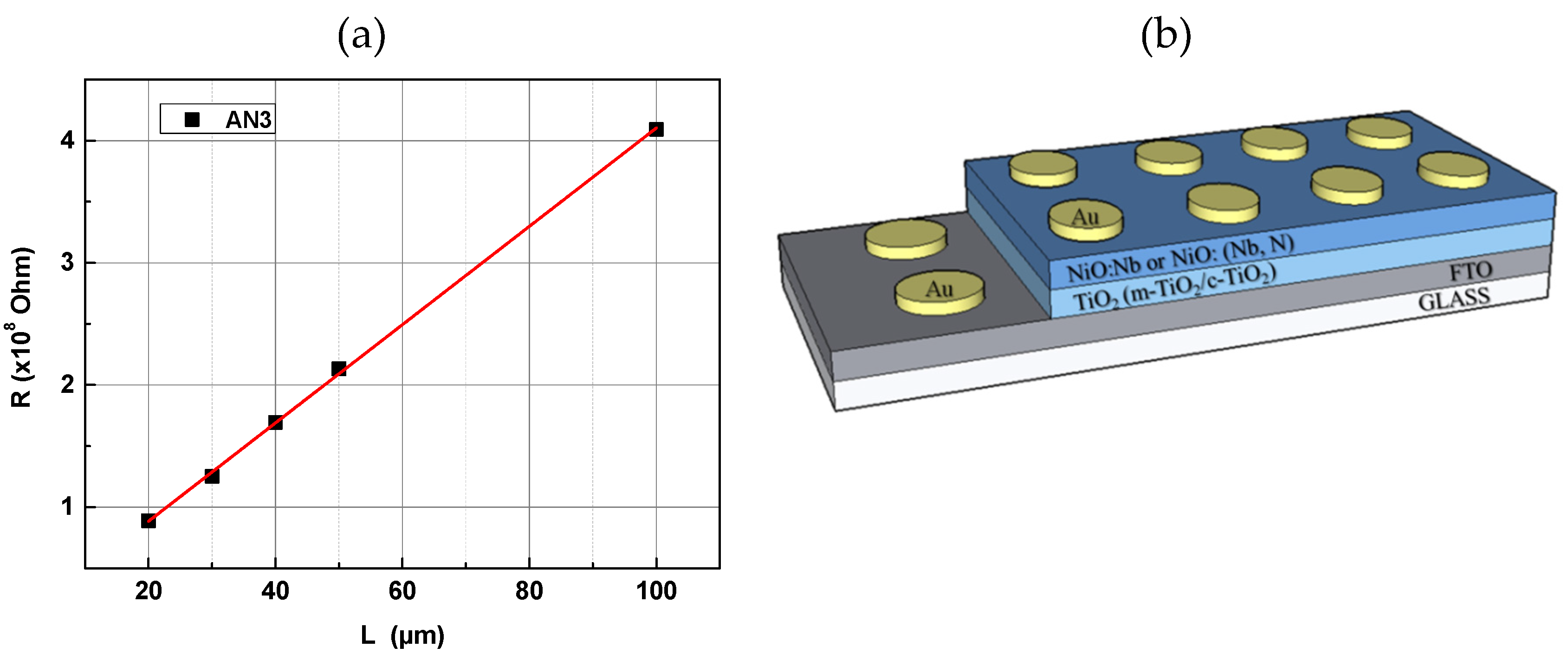
Figure 2.
(a) Wide-scan XPS spectra of NiO:Nb –AN film (Ar:O2:N2 = 50:50:0) and AN2 film (Ar:O2:N2=50:25:25). (b) and (c) Expansion of circled areas shown in (a) where the binding energies of Nb 3d and N 1s are located, respectively.
Figure 2.
(a) Wide-scan XPS spectra of NiO:Nb –AN film (Ar:O2:N2 = 50:50:0) and AN2 film (Ar:O2:N2=50:25:25). (b) and (c) Expansion of circled areas shown in (a) where the binding energies of Nb 3d and N 1s are located, respectively.
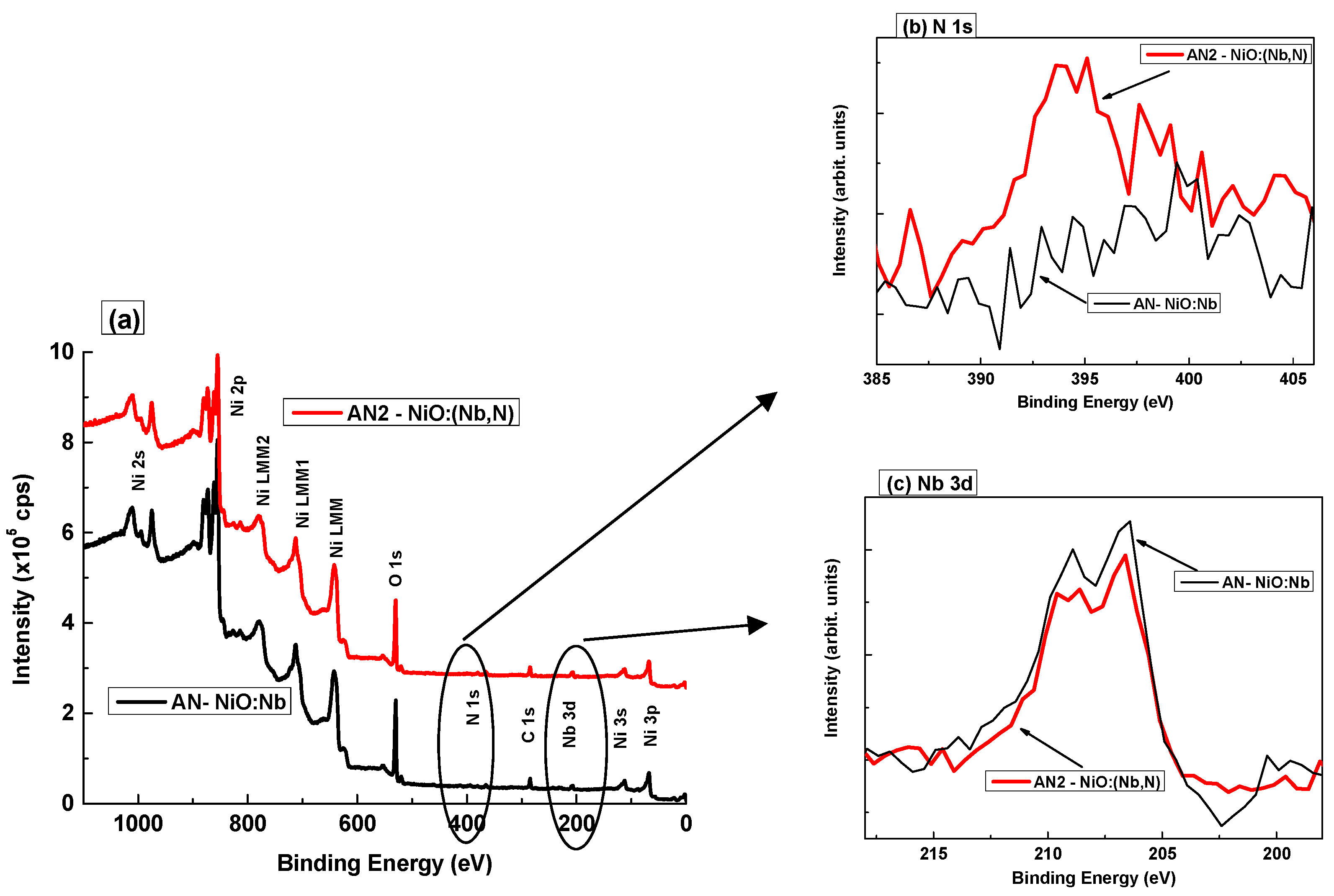
Figure 3.
(a) XRD patterns and (b) UV-Vis-NIR transmittance of as-prepared NiO:Nb -AN film and NiO:(Nb,N) films AN1, AN2 and AN3 deposited in decreasing % Ar gas in (Ar-O2-N2) plasma. The XRD lines of crystal NiO JCPDS card number 04-0835 is also shown in (a). The asterisks denote peaks from the Au pads (JCPDS: 040-0784).
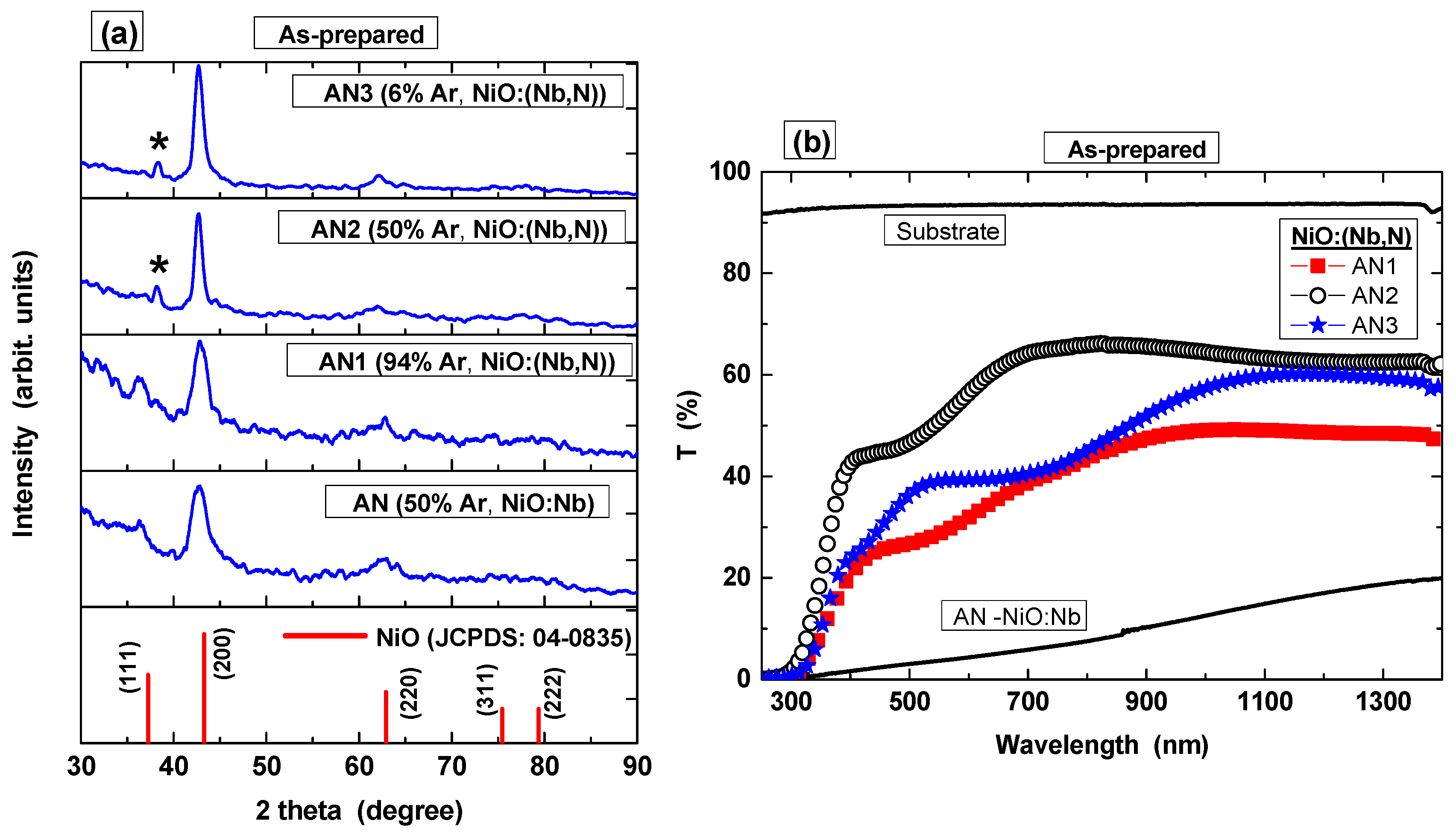
Figure 4.
Topography of double-doped NiO:(Nb,N) films deposited on Si substrates: (a) SEM and (b) AFM images.
Figure 4.
Topography of double-doped NiO:(Nb,N) films deposited on Si substrates: (a) SEM and (b) AFM images.

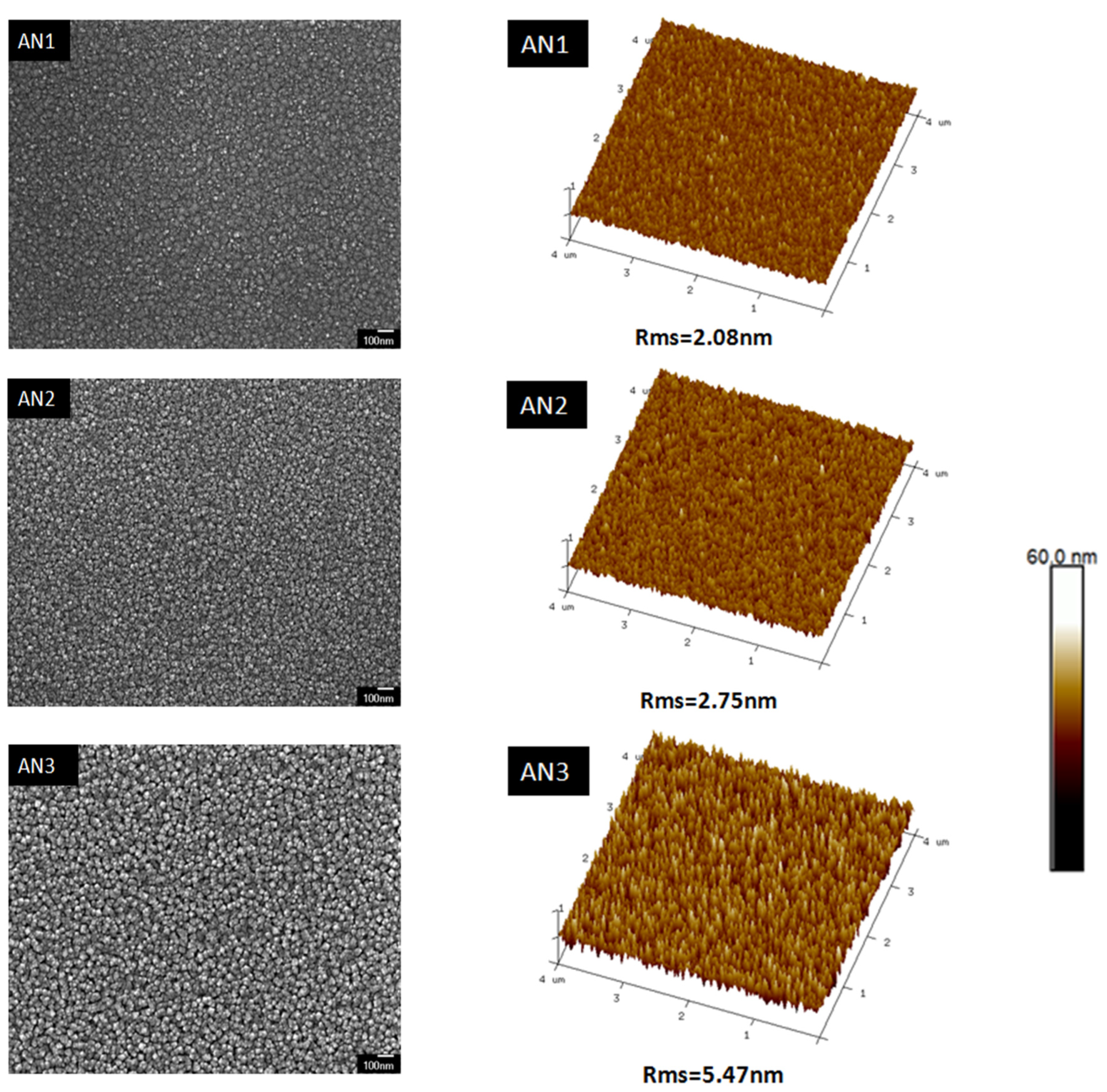
Figure 5.
XRD patterns of AN ref NiO:Nb film and NiO:(Nb,N) film AN1, AN2 and AN3 deposited in decreasing % Ar gas in (Ar-O2-N2) plasma after thermal treatment (TT1). The XRD lines of NiO JCPDS card number 04-0835 are also shown.
Figure 5.
XRD patterns of AN ref NiO:Nb film and NiO:(Nb,N) film AN1, AN2 and AN3 deposited in decreasing % Ar gas in (Ar-O2-N2) plasma after thermal treatment (TT1). The XRD lines of NiO JCPDS card number 04-0835 are also shown.
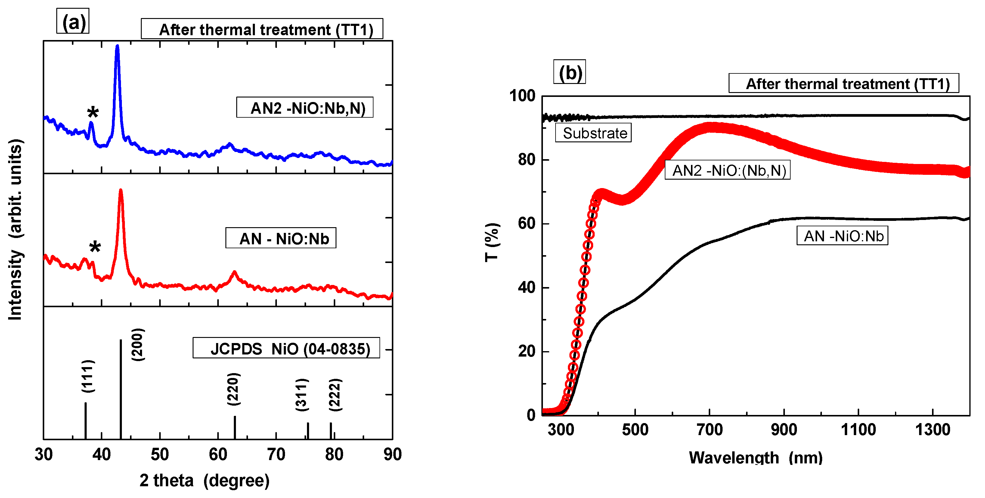
Figure 6.
(a) UV-Vis-NIR transmittance and (b) dark current density-voltage (Jd-V) of NiO:Nb/TiO2 and NiO:(Nb,N)/TiO2 diodes.
Figure 6.
(a) UV-Vis-NIR transmittance and (b) dark current density-voltage (Jd-V) of NiO:Nb/TiO2 and NiO:(Nb,N)/TiO2 diodes.
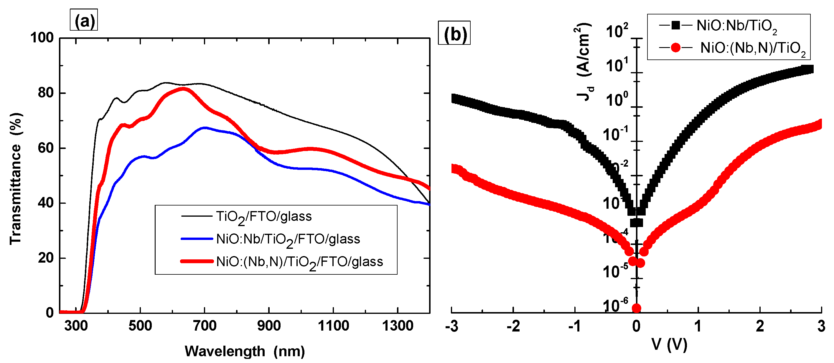
Figure 7.
Photo current density-voltage characteristics of the NiO:Nb/TiO2 and NiO:(Nb,N)/TiO2 heterodiodes under UV (λ = 325 nm) illumination. The Jph values of the NiO:Nb/TiO2 heterodiode are multiplied by x100 for better visibility.
Figure 7.
Photo current density-voltage characteristics of the NiO:Nb/TiO2 and NiO:(Nb,N)/TiO2 heterodiodes under UV (λ = 325 nm) illumination. The Jph values of the NiO:Nb/TiO2 heterodiode are multiplied by x100 for better visibility.
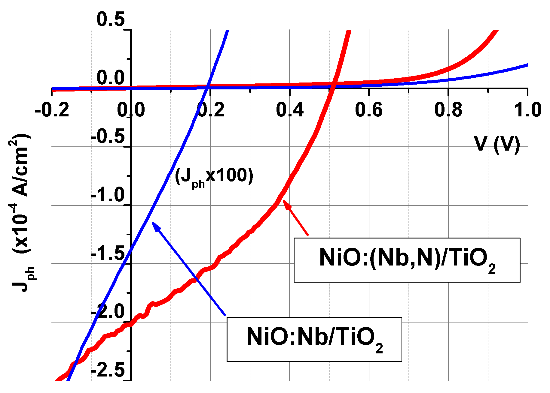

Table 1.
Deposition conditions of NiO-based films: single-doped NiO:(Nb) and double-doped NiO:(Nb,N). All depositions were made at the power of 300 W and total pressure of 0.67 Pa (5mTorr).
Table 1.
Deposition conditions of NiO-based films: single-doped NiO:(Nb) and double-doped NiO:(Nb,N). All depositions were made at the power of 300 W and total pressure of 0.67 Pa (5mTorr).
| NiO Films Sputtering conditions | NiO:Nb—Film AN | NiO:(Nb,N) | ||
|---|---|---|---|---|
| Film AN1 | Film AN2 | Film AN3 | ||
| Target | Ni-Nb | Ni-Nb | Ni-Nb | Ni-Nb |
| Gases flow rates (%) | Ar:O2:N2 = 50:50:0 |
Ar:O2:N2 = 94:3:3 |
Ar:O2:N2 = 50:25:25 |
Ar:O2:N2 = 6:47:47 |
| Deposition rate (nm/min) | 1.59 | 1.61 | 1.45 | 1.30 |
| Thickness (nm) | 175 | 161 | 164 | 186 |
| at.% Nb (Nb/(Ni+Nb)) | 3.5 | 3.8 | 2.4 | 1.4 |
| Substrates | Si (100) pieces, fused silica (1 mm thick), TiO2/FTO/glass | |||
Table 2.
Details of sputtering conditions and properties of as-prepared NiO:Nb and N-doped NiO:Nb films. D = crystallite size, εL = lattice strain, T = transmittance, Egap = energy gap, EU = Urbach energy.
Table 2.
Details of sputtering conditions and properties of as-prepared NiO:Nb and N-doped NiO:Nb films. D = crystallite size, εL = lattice strain, T = transmittance, Egap = energy gap, EU = Urbach energy.
|
As-prepared Films |
Deposition conditions |
Structural properties |
Optical properties |
|||||||
| Flow rates (%) | (200) peak 2θ (degree) |
D (nm) |
εL (x10-3) |
RMS roughness (nm) | Direct Egap (eV) | EU (meV) | ||||
| Ar | O2 | N2 | ||||||||
| NiO:Nb | AN | 50 | 50 | 0 | 42.58 | 4.7 | 20,9 | 2.11 | 3.25 | 2,734 |
| NiO:(Nb,N) | AN1 | 94 | 3 | 3 | 42.86 | 5.2 | 18.1 | 2.08 | 3.14 | 1,231 |
| AN2 | 50 | 25 | 25 | 42.69 | 8.9 | 9.2 | 2.75 | 3.67 | 557 | |
| AN3 | 6 | 47 | 47 | 42.72 | 7.7 | 12.2 | 5.47 | 3.21 | 812 | |
Table 4.
NiO:Nb/TiO2 and NiO:(Nb,N)/TiO2 diodes parameters as extracted from Figure 6b and using the I-V method. Jd(f) = current density at +3 V forward voltage, Jd(r) = current density at -3 V forward voltage, JS = saturation current density, RS = series resistance, n = ideality factor, φb = barrier height.
| NiO/TiO2 Diodes |
Jd(f)/Jd(r) (at ± 3 V) |
JS (A/cm2) |
RS (Ohm) |
n | φb (eV) |
|---|---|---|---|---|---|
| NiO:Nb/TiO2 | 7.2 | 1.8x10⁻³ | 13 | 7.0 | 0.58 |
| NiO:(Nb,N)/TiO2 | 19.1 | 1.0x10⁻⁵ | 351 | 8.2 | 0.71 |
Disclaimer/Publisher’s Note: The statements, opinions and data contained in all publications are solely those of the individual author(s) and contributor(s) and not of MDPI and/or the editor(s). MDPI and/or the editor(s) disclaim responsibility for any injury to people or property resulting from any ideas, methods, instructions or products referred to in the content. |
© 2024 by the authors. Licensee MDPI, Basel, Switzerland. This article is an open access article distributed under the terms and conditions of the Creative Commons Attribution (CC BY) license (http://creativecommons.org/licenses/by/4.0/).
Copyright: This open access article is published under a Creative Commons CC BY 4.0 license, which permit the free download, distribution, and reuse, provided that the author and preprint are cited in any reuse.


