1. Introduction
Photodetector (PD) is a key component in wide range of optoelectronic devices, such as optical signal receivers and optical communication in industrial applications [
1,
2,
3]. At present, most commercial PDs are fabricated based on the inorganic semiconductors such as Si, InGaAs, and GaN, which were capable of harvesting wide range of light from UV range (250–400 nm) to visible (450–800 nm) and infrared (900–1700 nm) range [
4]. Despite the inorganic semiconductor-based PDs were successfully demonstrated in their widespread applications, mechanical inflexibility and complex manufacturing processes impede their applications in current smart electronics such as wearable and deformable devices. In addition, the state-of-the-art device performance of the commercially available inorganic PDs are not satisfactory, thus recent research focuses on exploration of novel photoactive semiconductors with quick photoresponse, high sensitivity and detectivity to low brightness for high-performance PDs [
5].
Organolead trihalide perovskite has drawn increasing attention as a promising photoactive semiconductor due to its large optical absorption coefficient, long charge carrier lifetime and diffusion length, as well as low material cost, which strongly illustrates their considerable potential in PD applications [
6,
7,
8,
9,
10]. However, the solution-processed perovskite thin films usually possess a polycrystalline surface in which lots of boundaries, amorphous regions, and defect sites often exist. It has been revealed that the perovskite thin films from a solution casting usually exhibit much high-level of trap-state densities (>10
15 per cubic centimeter) as compared to the ideal single crystal states (~10
9 per cubic centimeter) [
11]. It has been studied that the imperfect lattices of defect site in the perovskite films become a recombination center, resulting in the decrease of electronic properties of the device to a great extent [
12,
13,
14]. In addition, the trap-state of perovskite film surface can induce non-radiative recombination for the photo-generated carriers, so undesirable energy loss and reduced steady-state charge flow of the perovskite thin film could be deteriorated under continuous device operation.
In order to improve the film quality and corresponding device performance of organoled trihalide perovskites, many methods have been put forwarded, including composite engineering, processing management, and additives employment during crystallization of perovskite crystal grains [
15]. These methods have been demonstrated to be effective in reduced defect densities of perovskite thin films and improved electronic properties of the corresponding devices in photovoltaic applications. In PDs, several processing engineering methods were investigated to improve film quality and corresponding electronic properties of the devices, but there was limited number of successful perovskite engineering for achieving high-performance perovskite PDs [
16].
Surface passivation is another viable strategy to improve film quality of organolead trihalide perovskite thin films. Since the distorted lattice structure of [PbI
6]
4− can become a defective antisite of organo lead trihalide perovskites, several passivating angents have been adopted in the field of perovskite photovoltaics [
17,
18,
19]. Among them, conjugated electron acceptors may be promising passivating molecules for stabilizing the defective antisites of perovskite film because those can accept free electrons from the undercoordinated dangling bonds or cation vacancies. For example, fullerene derivatives have acted as a Lewis acid for passivating undercoordinated iodide anions and PbI
3− antisites of the perovskite absorbers, achieving stabilization of the poervksite films and enhancement of the photovoltaic properties [
20]. Sargent and co-workers have demonstrated that the PC
61BM can be selectively incorporated at the grain boundaries of the polycrystalline perovskite films, so the halogen-rich trap sites at the grain boundaries was successfully passivated [
21]. Huettner and co-workers have also suggested that the PC
61BM molecules could be diffused into the perovskite layer to passivate iodine related defects [
22]. Thus, the fullerene-based perovskite passivation would be a key for reducing iodine ions/vacancies, and thus reducing the built-in field modulation for efficient charge transport in the device.
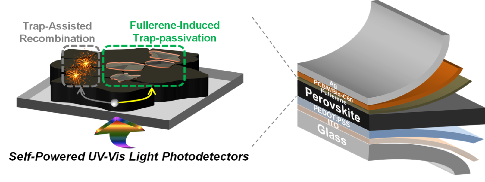
Inspired by these studies, we present a simple fullerene-passivation strategy to improve electronic properties of perovskite PDs. Fullerene can be dissolved in o-DCB for simple solution-processed surface passivation of MAPbI3 layer in which the defective antisites on the surface/grain boundaries were stabilized to facilitate charge extraction and transport to increase the electronic properties of device. As a result, the passivated perovskite films benefited from trap-state passivation in grain boundaries and defect sites as by fullerene-passivation, and the corresponding passivated perovskite PDs exhibited a wide spectrum span ranging from 350 to 750 nm, high responsivity (5 A W−1), specific detectivity (2 × 10¹³ Jones), and fast response (rise time 0.18 μs and fall time 17 μs) at zero bias. The self-powered perovskite PDs studied in this work may pave a way for improving electrical properties of light-detecting capability of PD device in the UV-Visible light region.
3. Results and Discussion
As described in the introduction, the organolead trihalide perovskites have a huge potential in PD applications due to excellent optoelectronic properties and potential in solution processing. As shown in
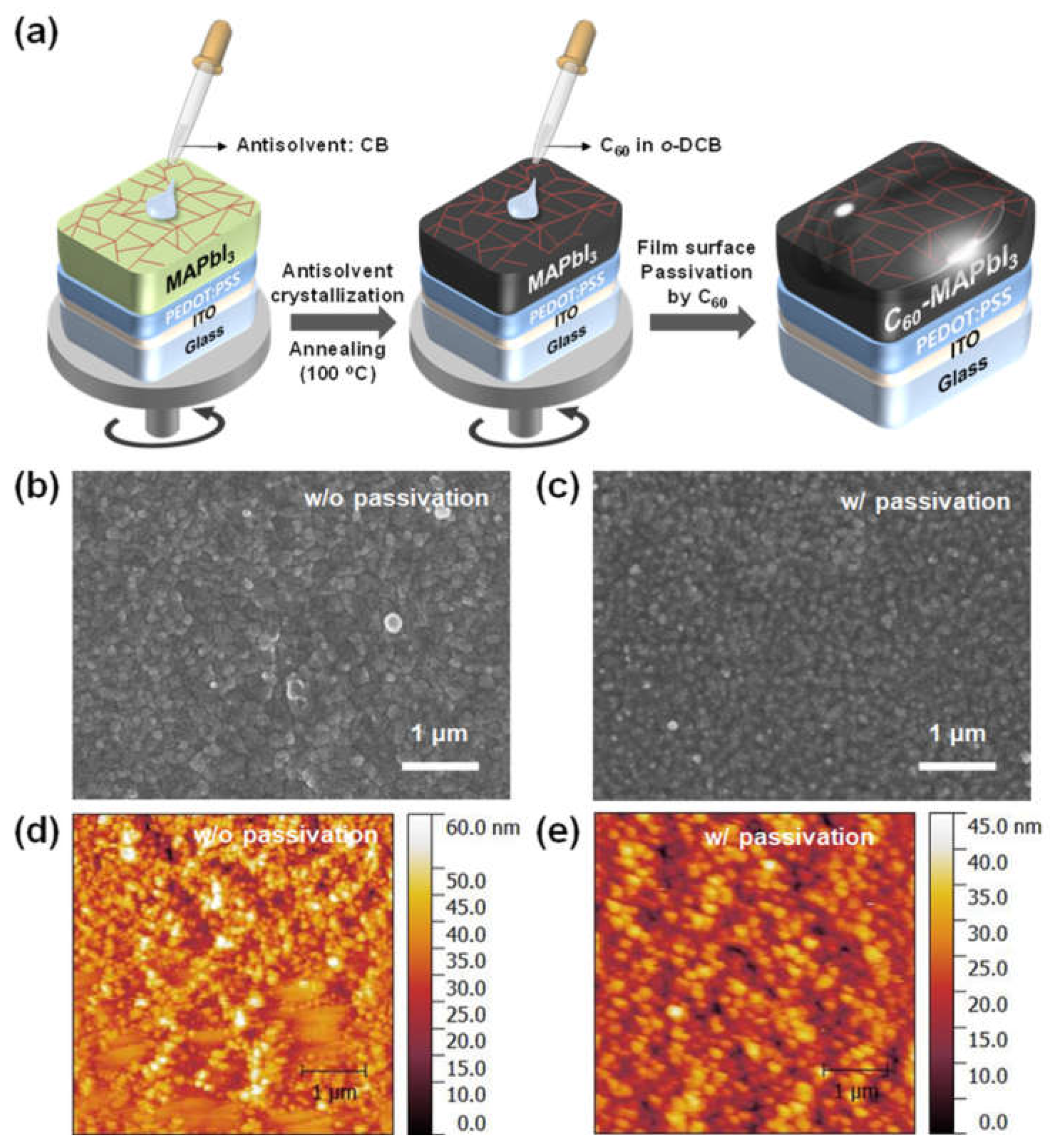
Figure 1a, polycrystalline MAPI
3 films were prepared by AAC process, followed by fullerene-passivation from a dilute solution of C
60 in
o-DCB [
23]. The film morphologies of MAPI
3 perovskite films were compared with respective of fullerene passivation.
Figure 1b,c present the surface morphology of perovskite films with and without fullerene passivation observed by FE-SEM. Two films exhibited nearly identical surface morphology of polycrystalline perovskite films in which compactly-grown grains with a grain size ranging from 200 to 250 nm were well grown over the substrate. (
Figure S1) We further studied the micro structure of the film surfaces of two MAPbI
3 films by using AFM.
Figure 1d,e displays the AFM topologies of the perovskite films, but the root-mean-square (RMS) roughness value varied from 21.3 nm to 8.4 nm for MAPbI
3 films as the fullerene-passivation was employed. Some defective areas were also seen in the pristine MAPbI
3 film while the passivated film possesses quite flat and uniform surface topology.
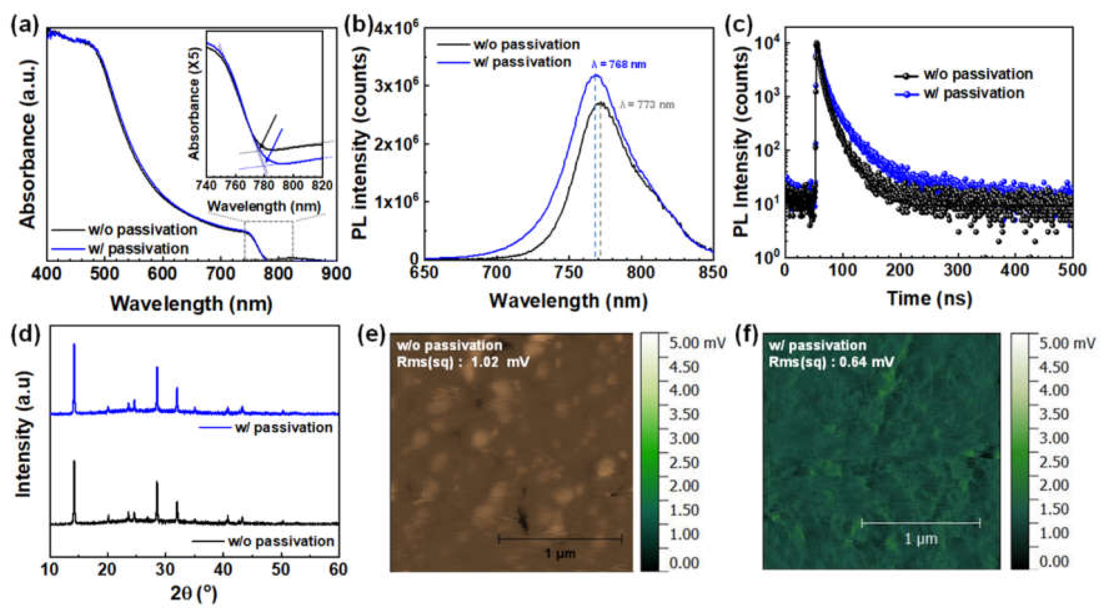
Benefitting from broadband absorption covering ultraviolet (UV) to visible range, MAPbI3 film is a feasible photon harvesting layer of UV-Vis broadband PDs. (
Figure 2a) The overall absorption spectra of two MAPbI
3 films were quite similar, where the absorption onsets of both films were slightly different. However, the band gap obtained from the Tauc plots of absorption spectra for two films were almost the same (
Eg = 1.61 eV). (
Figure S2) Thus, it is confirmed that the optical absorption property of MAPbI
3 perovskite film were hardly changed upon the fullerene passivation, which indicates that the optical properties of the MAPbI
3 films were hardly changed upon the fullerene passivation. Almost the same optical band gap of two films were further confirmed by the normalized steady-state photoluminescence (PL) spectra as shown in
Figure 2b that the PL peaks were centered at 768 and 773 nm for the perovskite film without and with passivation. Consistent with relatively increased PL intensity with the passivation, it is concluded that the non-radiative recombination at the defective site at the perovskite film surface was effectively suppressed by fullerene passivation. [
24] Time-correlated single photon counting (TCSPC) measurements of the perovskite films were compared to probe the photogenerated carrier dynamics upon the fullerene passivation (
Figure 2c). As summarized in
Table S1, the PL lifetime was increases with the fullerene passivation value from 35 to 68 ns. Considering the elongated PL lifetime and enhanced PL intensity, the fullerene passivation effectively tailors the carrier recombination behavior, which will influence the electronic properties of PD device. We also performed X-ray diffraction (XRD) measurement of the films to characterize the crystallinity of the perovskite absorber upon the fullerene passivation. As displayed in the XRD diffractograms of
Figure 2d, we observed a clear evolution of the perovskite crystal structures with obvious characteristic peaks at 14.2°, 28.6°, 31.02°, and 43.38°, which are assigned to the (110), (220), (310), and (330) planes. The XRD result reveals predominant orthorhombic crystal structure regardless of the passivation by fullerene.
We further investigate Kelvin probe force microscopy (KPFM) of the perovskite films to elucidate the passivation effect of the fullerene on the perovskite absorber. The local surface potential of two films has are displayed in
Figure 2e,f. The KPFM provides a reliable measurement of local surface potentials stemming from contact potential differences (CPD) between the tip and sample surface associated with their relative work functions. (
Figure S3) However, there was negligible CPD difference in the MAPbI
3 films regardless of fullerene passivation, indicating that the fullerene passivation does not significantly affect the electronic structure of the perovskite films. However, These grain-to-grain variations in the CPD was observed in the MAPbI
3 film without the passivation, while the passivated film possessed more smooth surface potential over the film surface, which thereby reveals that the local potential well that becomes a barrier for charge transport would be effectively removed [
25].
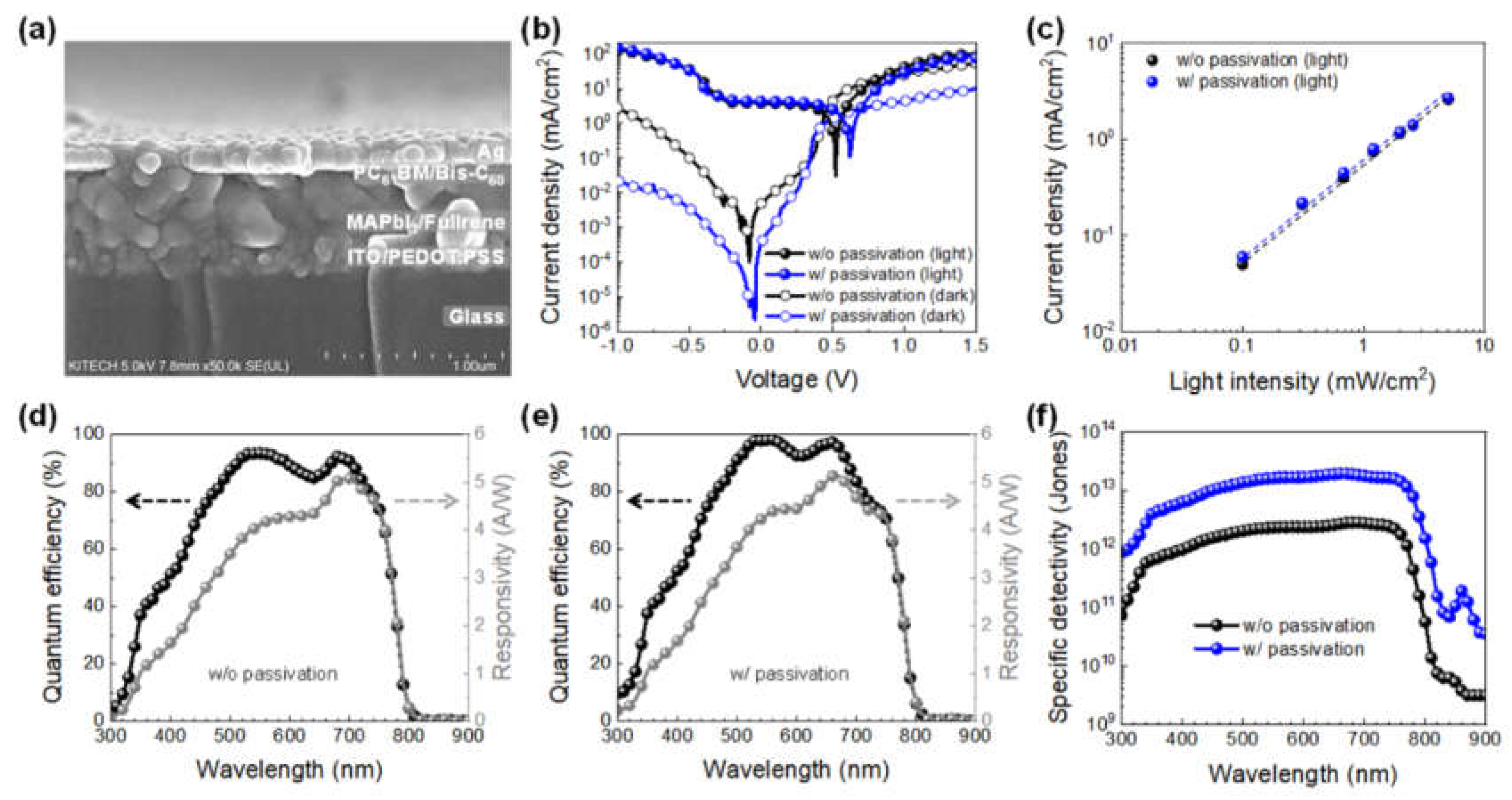
In order to verify the fullerene passivation effect on the device properties of perovskite PDs, we primitively fabricated the device with a
p-i-n structure. The device structure was confirmed by cross-sectional SEM image as present in
Figure 3a. The perovskite PDs are composed of a sandwich structure of
p-i-n configuration in which PEDOT:PSS and PC
61BM were incorporated as a hole transport layer and an electron transport layer, respectively. ITO and Ag were used as an anode and a cathode, respectively, to maximize the internal field of device for exciton dissociation at the perovskite absorber layer. It is noted that Bis-C60 was used as a cathode modifier to reduce the charge recombination as well as the leakage current under reverse bias, which is particularly important for photodetectors for high gain [
26].
Figure 3b displays the current density–voltage (
J–
V) curves measured in the dark and under illumination condition (illumination of 100 mW cm
−2 (1.5G Air Mass)) with a bias ranging in −1.0 to 1.5 V. The dark current density of the pristine device was as low as 10
−3−10
−4 mA/cm
2 at zero or low bias (−0.1 V), which was further reduced to 10
−5−10
−6 mA cm
−2 after fullerene passivation. The substantially reduced dark current for the fullerene-passivated devices were mainly originated from the defect density for the MAPbI
3 layer. The space charge limited current (SCLC) characterizations of two MAPbI
3 films were present in Supplementary data (
Figure S4). The trap-filled limit voltage (
VTFL) decreases from 0.27 V to 0.20 V through fullerene-passivation, so the trap density in the devices correspondingly reduced from 1.04 × 10
12 cm
−3 to 7.70 × 10
13 cm
−3, respectively. It is thus expected that the trap-assisted recombination would be suppressed in the passivated MAPbI
3-based device, resulting in stabilization of the dark current.
The photocurrents of two devices were comparable in varied intensity of white light illumination (0.1 to 3 mW cm
−2), as shown in
Figure 3c. The relationship of photocurrent density of the device versus irradiation light intensity at 0 V can be described by a power law,
Jph ~
Pα, where
Jph is the photocurrent density,
P is the light intensity, and
α is the exponent. The fitted line of device describes an exponential relationship of
α ~ 1.06 and 1.02 for the device without and with the passivation. The lower
α value of the power low reveals near-linear dependency of the photocurrent on the light intensity of the passivated device, which further verifies lower recombination rate of the fullerene passivation of the MAPbI
3 layer.
In order to benchmark the photodetecting properties of the device, two key criteria (spectral responsivity (
Rλ) and EQE) were mainly investigated. The spectral responsivity indicates how the photodetecting device efficiently responds to incident photon, as defined by following eqution.
Jph is the photocurrent density,
I is the intensity of the incident photon, EQE is the quantum efficiency of the device to the wavelength (
λ).
Figure 3d displays the EQE spectra and spectral responsivity of the pristine device at different wavelength at a zero bias. The non-passivated MAPbI
3-based device exhibited a broad photoresponse from 300 to 800 nm with a peak EQE of 93%, and the spectral responsivities of 3−5 A W
−1 at the wavelength range from 450 to 750 nm. In the case of fullerene passivation, the device exhibited slightly higher EQE of 97%, but the spectral responsivity was similar to that of the pristine one (of 3−5 A W
−1), indicating the excellent photoresponse performance of the devices due to high crystalline properties of MAPbI
3 regardless of passivation. (
Figure 3e) Another figure of merit of PDs is specific detectivity (
D*), so the detectivity of two devices were compared, assuming that shot noise is a major source of the noise. [
27,
28] As shown in
Figure 3f, the detectivity was calculated using the following equation:
where
R is the spectral responsivity,
A is the active device,
e is the elementary charge, and
Jdark is the dark current. The detectivity of the passivated device was as high as 2 × 10
13 Jones in the range of 350−760 nm, which is notably higher than that of the pristine one (~10
12 Jones) at a zero bias. The noise equivalent power (NEP) is another key parameter representing the electronic performance of PD. NEP can be estimated based on the measured dark current noise (
in) and the
Rλ of the devices as followed:
It is noted that the noise current of the PDs is mainly composed of shot noise and thermal noise, however the shot noise could be negligible for the self-powered device (operation at 0 V). Thus, the thermal noise is the most dominant noise in this study [
29]. The thermal noise can be expressed as followed:
where
kB is the Boltzmann constant,
T is the temperature, and
R is the resistance of the device as extracted from the dark current−voltage curves at 0 V. The noise currents were calculated to be 0.315 and 0.143 pA Hz
−1/2 for the pristine and the passivated device, respectively, and the corresponding NEPs at 550 nm were 0.063 and 0.028 pW for the pristine and the passivated one, respectively. The NEP is a figure-of-merit for quantifying the sensitivity of PDs, so such a low NEP for the passivated MAPbI
3-based PDs implies that the fullerene passivation facilitates the light-detecting capability of very low intensities, but also helps to outperform commercial silicon diodes and perovskite photodetectors reported in literature in terms of noise current and NEP [
30].
Not only NEP, linear dynamic range (LDR) is a standard metric of in most PD applications, such as image sensors. The NDR values characterizes the light intensity range in which the photodetectors have a constant responsivity, which can be expressed as followed:
where
J*ph is the photocurrent of the device measured at light intensity of 1 mW cm
−2 and
Jd is the dark current. As shown in
Figure 3b,c, two MAPbI
3-based PD showed similar linear photoresponse at light intensities ranging from 0.03 to 4 mW cm
−2, but the LDR values for the devices were 64 and 110 dB without and with the fullerene passivation, respectively. It is noteworthy that the LDR value for the passivated device was higher than that of InGaAs photodetector (66 dB), and comparable to that of Si photodiode (120 dB) [
31]. Additionally, this was better than the perovskite PDs with the interface engineering (~100 dB) as reported elsewhere [
30]. Thus, we emphasize again that the fullerene-passivation significantly improves the optoelectronic properties of the perovskite PDs in terms of detectivity and NEP.
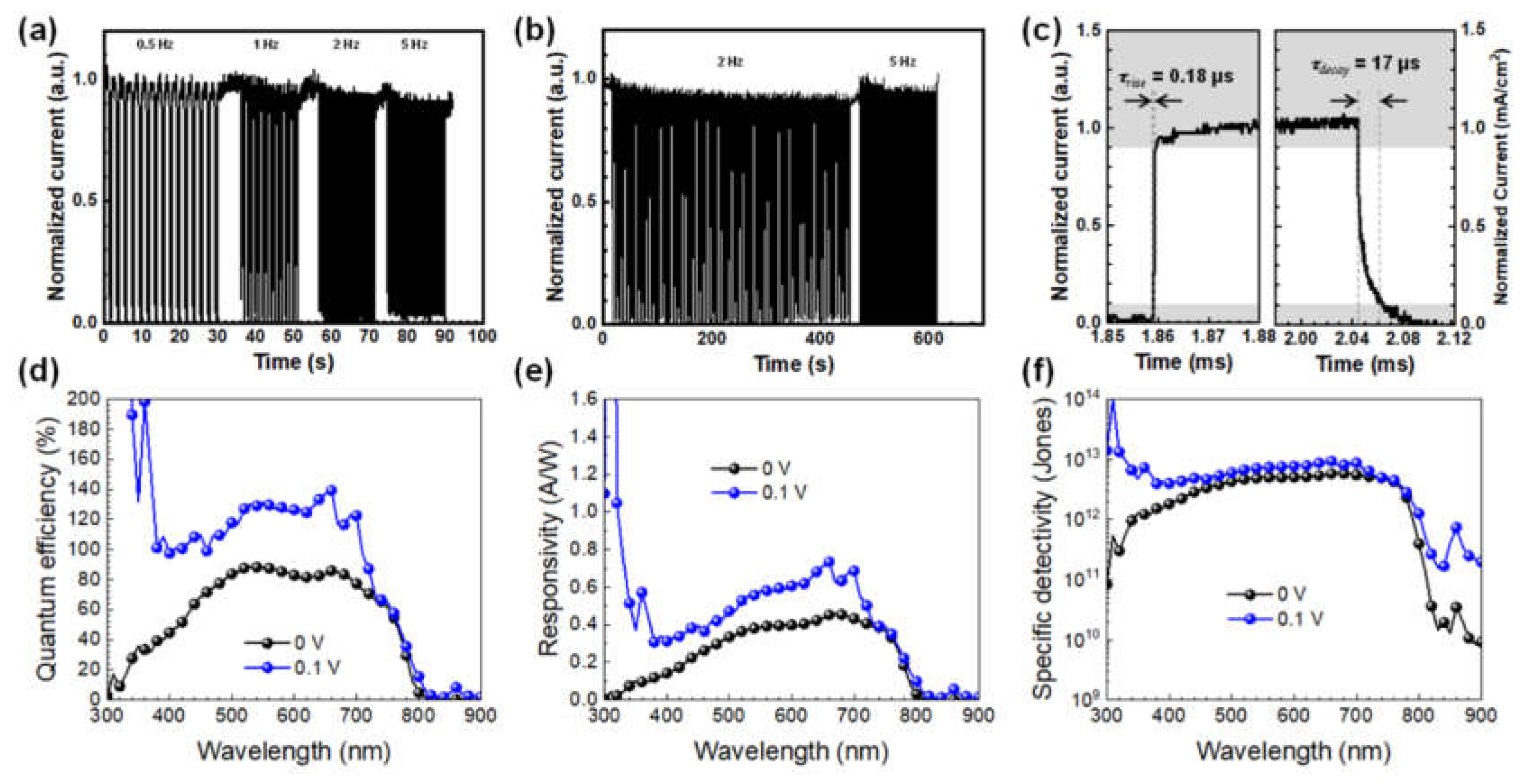
We then examined the temporal response behavior of the fullerene-passivated perovskite PDs.
Figure 4a displays the time-resolved photoresponse of the fullerene-passivated perovskite PD with varied modulation frequency of the illumination (white light (3 mW cm
−2)) at zero bias, illustrating a good photo-switching property of the device. One can see that the device exhibits a prompt and reproducible photocurrent response with a good cycling stability, and meanwhile, as the frequency of a light increases from 0.5 to 5 Hz. The passivated devices exhibited reliable photoresponse performance for 600 s as shown in
Figure 4b. To explore the photoresponse speed, the time-resolved photoresponse at on and off state was magnified, as shown in
Figure 4c. The response graph of the device exhibited steep rise and fall edges, which not only imply a rapid response rate of PD device but also reveals fast separation/collection process of the photo-generated carriers in device. The rise time (
τrise) is defined as a time period for the photocurrent increasing from 10 to 90% of its steady-state value, whereas the decay time (
τdecay) is defined as a time period for the photocurrent decreasing from 90 to 10% of its steady value. In the passivated device, the rise and decay times were 0.18 and 17 μs, respectively, which reflects the ability to follow fast optical signal in various applications. It is noteworthy that the response time of the fullerene-passivated PDs is much faster than those of perovskite-based PDs reported in literatures (
Table S1). The superior photoresponse performance of the fullerene-passivated MAPbI
3 PDs may be attributed to reduced defect density in the film surface/grain boundaries of MAPbI
3, which facilitated efficient charge transport and suppressed charge recombination at the interfaces of the device
Lastly, we compared the photodetecting properties of the passivated device with and without bias voltage to examine the capability of the self-powered device operation.
Figure 4d,f compare the EQE, responsivity, and detectivity of the passivated-device at different bias voltages (zero and 0.1 V). It is definitely, the device showed more photon-to-electron conversion in 300–700 nm due to the stronger external electrical field, and a similar phenomenon was also observed in the spectral responsivity, as expected. However, the order of enhancement is not so impressive, and thus the detectivity of the device under a bias of 0.1 V was similar in the entire range of photon harvesting for MAPbI
3 (~10
12 Jones in 350–750 nm). According to the EQE, responsivity, and detectivity, the fullerene passivation is more valuable when the device is operated without operating power. Thus, it is clear that the fullerene passivation strategy is promising for further improvements in the performance of perovskite-based PDs requiring self-powered operation.