
Submitted:
19 November 2025
Posted:
24 November 2025
You are already at the latest version
Abstract
Boron incorporation in gallium nitride (GaN) semiconductors affects their physical properties, such as the bandgap and lattice parameters. However, the macroscopic electrical behavior of BGaN remains largely unexplored. In this study, Mg-doped p-type BGaN epitaxial layers were grown by metal–organic chemical vapor deposition (MOCVD) and characterized using Hall effect and van der Pauw measurements over a temperature range from liquid nitrogen temperature up to 277°C. The results reveal a monotonic dependence of conductivity on temperature, consistent with nearest-neighbor hopping (NNH) conduction, quite similar to that observed in Mg-doped GaN. Unlike in BGaN, the transition between NNH and free-carrier conductivity occurs at a higher temperature, which is attributed to a higher defect concentration. These findings provide new insight into how boron incorporation influences the electronic properties of gallium nitride–based materials and offer valuable guidance for future electronic and optoelectronic applications.
Keywords:
BGaN
; charge transport properties
; hall effect measurement
1. Introduction
Ternary BGaN and quaternary BInGaN compounds are currently of interest because Boron can affect the physical properties of GaN-based nitrides, especially their bandgap, lattice parameters and dielectric constant. BGaN compounds may then be useful for the production of new electronic or optoelectronic devices [1,2,3,4,5]. Although the optical properties of BGaN have been previously described in the literature, their electrical properties remain largely unexplored and undescribed.There are some papers devoted to studies of B influence on structural and optical properties of BGaN [6,7], and dependence of B concentration in BGaN layer on crystal growth conditions [4]. As was recently revealed, the B concentration in BGaN grown by Chemical Vapor Deposition (CVD) methods depends strongly on growth temperature [8]. At a low growth temperature of 700 °C, B concentration can reach a few percent, but increasing temperature to near 1100 °C, the concentration reduces reasonably near or below 1% [8]. Nevertheless, such boron content significantly increases the electrical resistivity as it causes the formation of deep defects, which leads to a resistivity of 105 Ωcm, characteristic of a semi-insulating material. Although unusual changes in resistivity of BGaN films versus B concentration have been partially characterized [9], BGaN layers intentionally doped for n- and p-type have not been found in the literature so far. The effect of boron on p-type conductivity GaN is investigated here for the first time. We characterize electrical transport properties of Mg-doped BGaN film using van der Pauw and Hall effect methods in temperature range from -192 °C (LN2) up to 277 °C. The main aim of the experimental research on the properties of electric transport is to compare the macroscopic electrical properties of p- type doped BGaN, with those of the well-known properties of p-type GaN.
2. Experimental
BGaN epitaxial structures were fabricated using the AIX 200/4 RF-S reactor MOCVD from AIXTRON. The multilayer stack consisted of AlN(NL)/AlN/GaN/GaN:Si/BGaN:Mg was grown on Cryscore 2″ Al2O3 substrates with 0001 SSP orientation. Before the growth, substrate was annealed in N2 at 850 °C for 30 min. Next an AlN nucleation layer (NL) was deposited at 715 °C, 50 mbar, followed by an AlN layer (727 nm) grown at 1180 °C, 50 mbar. A GaN layer (636 nm) was deposited at 1140 °C, 200 mbar, and the final BGaN:Mg layer was grown at 1050 °C and a pressure of 900 mbar, using TEB, TMGa, NH3, and Cp2Mg precursors.
Electrical properties were characterized using a Hall Effect Measurement System (HMS5000/AMP55T) with the Van der Pauw method. The system measures carrier concentration, mobility, resistivity, and Hall coefficient over a temperature range from 80 K to 550 K under a 0.55 T magnetic field, it is compatible with square samples with edge length in range from 5 mm to 20 mm.
3. Results and Discussion
Hopping conduction among impurity sites remains a subject of ongoing debate and is not yet fully understood in doped GaN materials. In particular, the dependence of the Hall coefficient on hopping transport mechanisms still requires further investigation [11]. This uncertainty arises mainly from the insufficient number of experimental studies that could validate existing theoretical models. However, it is worth mentioning, for example, the experimental works described in [11,12,13,14,15,16], which provide valuable experimental analyses of this topic. The lack of data is especially evident for highly resistive BGaN materials, which have so far not been extensively investigated so far.
In group III and IV semiconductors (such as GaN), the ionization energies of hydrogen-like impurities are relatively high due to the large effective masses of charge carriers [11]. Consequently, hopping conduction between impurity sites becomes more prominent [17].
Therefore, a key part of our research was to investigate the electrical properties and conduction mechanisms in Mg-doped p-type BGaN and Si-doped n-type BGaN, using Hall effect measurements across a range of temperatures. Before presenting the results from this part of our study, we would like to summarize—following [11], the existing conduction models and provide a brief overview of the topic. In our description, we adopt the view that the measured conductivity (σ) is a simple sum [11] of contributions from both hopping transport and conventional free carrier transport as follow
A similar relationship is observed in the case of the Hall coefficient
where refers to conductivity, stands for the Hall coefficient and the indexes: hop, f—refer to hopping and free carrier contributions, respectively.
The proportion between free carrier and hopping conduction changes with temperature. Therefore, by adjusting the temperature range during measurements, we can gain insights into which conduction mechanism is dominant under specific conditions. This analysis was performed, and the results are presented later in this section.
Before discussing the results, we would also like to highlight again, based on [11], the main mechanisms of hopping conductivity. At least three distinct types of hopping conduction can be identified, which are characterized by different temperature dependencies [11,18]: Efros—Shklovskii (E-F) Variable Range Hopping (VRH), Mott Variable—Range Hopping (VRH) and—nearest neighbor hopping (NNH).
In the case of the E-F VRH we can expect a linear relationship of the against the , since the hopping conductivity
and the , mobility of the hopping carrier of charges is given by the
where T is the temperature, and the , are adjustable parameters [11]. This type of electric transport is more likely to occur in the case of the n-doped GaN [11,19,20]. In [11] this relationship, was fitted to the mobility data from measurements, which made it possible to distinguish the change from free carrier mechanism to the hopping conductivity at around , in case of Si-doped GaN. Measurements of BGaN at such low temperatures were inconsistent due to a significant increase in resistance. Therefore, in the case of Si-doped BGaN, we are only able to state that within the available temperature range , we observed a single conduction mechanism. Based on comparisons with existing research [6] and the typical behavior of conductivity, this mechanism is attributed to free carrier transport.
In the case of p-doped group III and IV semiconductors, such as Mg-doped BGaN, the dominant hopping transport mechanism is nearest-neighbor hopping (NNH) [11,21,22,23,24,25]. The NNH model was fitted specifically for Mg-doped GaN in [11]. Similarly to the E–S VRH the dependence from the temperature dependence can be used as an indication of the transition from free carrier conduction to the NNH. In the case of the NNH one expect the linear dependency
against the [6]. Since in the case of the NNH [11]
In our case we obtained linear, characteristic for NNH and the transition at temperature around 245 K, which is a little bit higher than the temperature ~190 K, obtained in the work [11] for Mg doped GaN. In Figure 1. we present the fitted dependence of the for Mg doped BGaN sample.
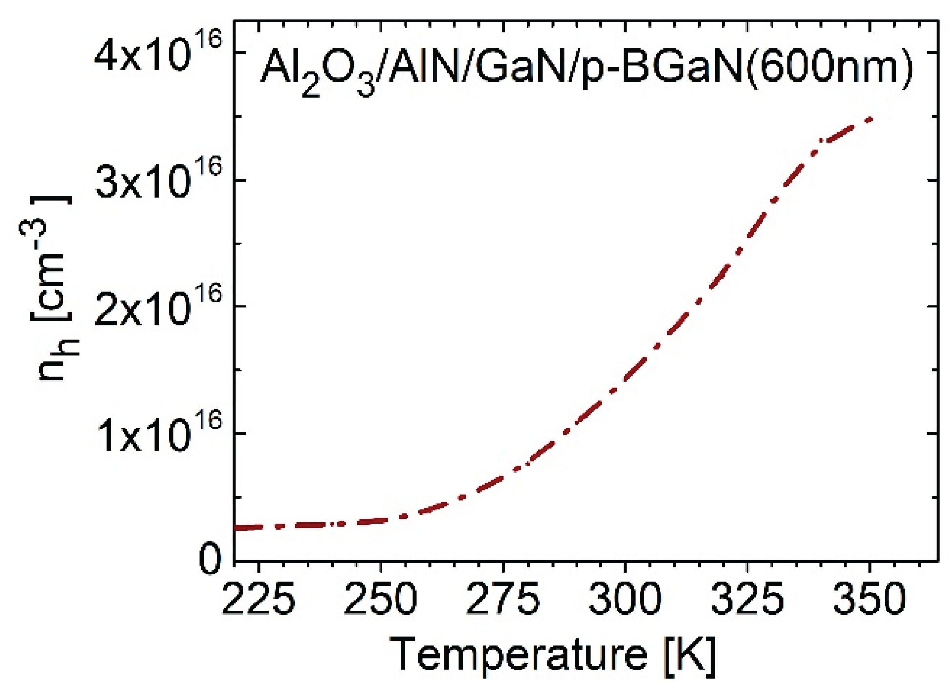
Additional Hall measurement was conducted for higher temperatures, up to 540 K, and it confirmed the linear dependence of the function versus inversed temperature. Figure 2 presents the resistivity of the p-BGaN layer as a function of temperature. The resistivity decreases with increasing temperature, which is attributed to the rising concentration of charge carriers. This behavior is illustrated in Figure 3 and it is characteristic for holes concentrations and free carrier transport in this temperature range. However, the hole concentration seems not to be high enough for a hole injection layer in the LED structure, but such a layer can work promisingly as an EBL (electron blocking layer) layer in UV LEDs build on the BGaN n-p junction leading to a reasonable increase in the quantum efficiency of the electroluminescence diode [26].
4. Conclusions
In summary, Hall measurements performed in the van der Pauw configuration revealed a relationship between the macroscopic electrical parameters of Mg-doped BGaN comparable to that observed in p-type GaN [11]. A linear dependence of conductivity on temperature was identified, providing further evidence of nearest-neighbor hopping (NNH) conduction in p-BGaN, analogous to that in p-GaN. Notably, the transition from NNH to free-carrier conduction occurs in p-BGaN at a higher temperature than in p-GaN, which may be attributed to defects with reasonable concentrations in BGaN layers as they were recently observed and published [8].
Acknowledgments
The work was founded by the R.N. Łukasiewicz Centre through Grant Number 4/Ł-IMIF/CŁ/2021.
References
- Rather, M.A.; Ravi, L.; et al. An experimental study of the energy band alignments of B(Al, Ga)N heterojunctions. Appl. Phys. Lett. 2023, 123, 012101. [Google Scholar] [CrossRef]
- Williams, L.; Kioupakis, E. BInGaN alloys nearly lattice-matched to GaN for high-power high-efficiency visible LEDs. Appl. Phys. Lett. 2017, 111, 211107. [Google Scholar] [CrossRef]
- Turiansky, M.E.; Shen, J.-X.; Wickramaratne, D.; Van de Walle, C.G. First-principles study of bandgap bowing in BGaN alloys. J. Appl. Phys. 2019, 126, 095706. [Google Scholar] [CrossRef]
- AlQatari, F.; Liao, C.-H.; Li, X. Demonstration of MOCVD-grown BGaN with over 10% boron composition. AIP Adv. 2022, 12, 085318. [Google Scholar] [CrossRef]
- Shen, J.-X.; Turiansky, M.E.; Wickramaratne, D.; Van de Walle, C.G. Thermodynamics of boron incorporation in BGaN. Phys. Rev. Mater. 2021, 5, L030401. [Google Scholar] [CrossRef]
- Gunning, B.P.; Moseley, M.W.; Koleske, D.D.; Allerman, A.A.; Lee, S.R. Phase degradation in BxGa1−xN films grown at low temperature by metalorganic vapor phase epitaxy. J. Cryst. Growth 2017, 464, 190. [Google Scholar] [CrossRef]
- Zdanowicz, E.; Iida, D.; Pawlaczyk, L.; Serafinczuk, J.; Szukiewicz, R.; Kudrawiec, R.; Hommel, D.; Ohkawa, K. Boron influence on bandgap and photoluminescence in BGaN grown on AlN. J. Appl. Phys. 2020, 127, 165703. [Google Scholar] [CrossRef]
- Mozdzynska, E.B.; Kaminski, P.; Kozłowski, R.; et al. Effect of the growth temperature on the formation of deep-level defects and optical properties of epitaxial BGaN. J. Mater. Sci. 2022, 57, 17347. [Google Scholar] [CrossRef]
- Baghdadli, T.; Ould Saad Hamady, S.; Gautier, S.; et al. Electrical and structural characterizations of BGaN thin films grown by metal-organic vapor-phase epitaxy. Phys. Status Solidi C. [CrossRef]
- Mozdzynska, E.B.; Złotnik, S.; Ciepielewski, P.; Gaca, J.; Wojcik, M.; Michałowski, P.P.; Rosinski, K.; Pietak, K.; Rudzinski, M.; Jezierska, E.; et al. Insights on boron impact on structural characteristics in epitaxially grown BGaN. J. Mater. Sci. 2022, 57, 7265–7275. [Google Scholar] [CrossRef]
- Kajikawa, Y. Analysis of the Hall-effect data on Mn-doped GaAs with taking into account the Hall factor for nearest-neighbor hopping conduction. Phys. Status Solidi C 2016, 13(5–6), 387–394.
- Wolos, A.; Wilamowski, Z.; Piersa, M.; Strupinski, W.; Lucznik, B.; Grzegory, I.; Porowski, S. Properties of metal-insulator transition and electron spin relaxation in GaN:Si. Phys. Rev. B 2011, 83, 165206. [Google Scholar] [CrossRef]
- Gunning, B.; Lowder, J.; Moseley, M.; Doolittle, W.A. Negligible carrier freeze-out facilitated by impurity band conduction in highly p-type GaN. Appl. Phys. Lett. 2012, 101, 082106. [Google Scholar] [CrossRef]
- Lancefield, D.; Eshghi, H. Temperature-dependent hole transport in GaN. J. Phys.: Condens. Matter, 2001, 13(39), 8939–8947. [Google Scholar]
- Kinoshita, T.; Obata, T.; Yanagi, H.; Inoue, S. High p-type conduction in high-Al content Mg-doped AlGaN. Appl. Phys. Lett. 2013, 102(9), 092109. [Google Scholar] [CrossRef]
- Chen, C.-C.; Lin, Y.-R.; Lin, Y.-W.; Su, Y.-C.; Chen, C.-C.; Huang, T.-C.; Wu, P.-H.; Yang, C. C.; Mou, S.; Averett, K. L. Improvement of p-type AlGaN conductivity with an alternating Mg-doped/undoped AlGaN layer structure. Micromachines 2020, 11(6), 598. [Google Scholar]
- Neumann, H. Influence of impurity band conduction on the electrical characteristics of p-type GaAs. Cryst. Res. Technol. 1988, 23, 1377. [Google Scholar] [CrossRef]
- Shklovskii, B.I.; Efros, A.L. Electronic Properties of Doped Semiconductors; Springer-Verlag: Berlin, Germany, 1984. [Google Scholar]
- Koon, D.W.; Castner, T.G. Variable-range hopping and the Hall coefficient in Si:As. Solid State Commun. 1987, 64(11).
- Mansfield, R. In Hopping Transport in Solids; Pollak, M. , Shklovskii, B.I., Eds.; Elsevier: Amsterdam, The Netherlands, 1991; p. 349. [Google Scholar]
- Bezaquen, M.; Belache, B.; Blaauw, C. Electrical properties of Cd-doped and Mg-doped InP. Phys. Rev. B 1992, 46, 6732. [Google Scholar] [CrossRef] [PubMed]
- Korona, K.P.; Wysmolek, A.; Kamińska, M.; Twardowski, A.; Piersa, M.; Palczewska, M.; Strzelecka, G.; Hurban, A.; Khul, J.; Adomavicius, R.; Krotkus, A. Manganese as a fast charge carrier trapping center in InP. Physica B: Condens. Matter 2006, 382, 220–228. [Google Scholar] [CrossRef]
- Kurilenko, I.N.; Litvak–Gorskaya, L.B.; Lugovaya, G.E. Conductivity via deep impurity centers in p-InSb. Sov. Phys. Semicond. 1980, 13, 906. [Google Scholar]
- Obukhov, S.A. Nonlinear electrical properties of a system of strongly correlated electrons in a strong magnetic field. Phys. Status Solidi B 2005, 242, 1298. [Google Scholar] [CrossRef]
- Wolos, A.; Piersa, M.; Strzelecka, G.; Korona, K.P.; Hurban, A.; Kamińska, M. Mn configuration in III–V semiconductors and its influence on electric transport and semiconductor magnetism. Phys. Status Solidi C 2009, 6, 2769. [Google Scholar] [CrossRef]
- Bashir, J.; Usman, M.; Sengouga, N.; Hassani, M. Introducing boron gallium nitride as carriers’ source layer for efficient near-ultraviolet microLED. Phys. Scr. 2024, 99 125534. [Google Scholar]
Figure 1.
Natural logarithm of the product of conductivity and temperature (ln(σ · T3ᐟ2) plotted as a function of inversed temperature (1/Temperature). The graph indicates a transition from nearest-neighbor hopping (NNH) conduction to free carrier transport for temperatures above 245 K.
Figure 1.
Natural logarithm of the product of conductivity and temperature (ln(σ · T3ᐟ2) plotted as a function of inversed temperature (1/Temperature). The graph indicates a transition from nearest-neighbor hopping (NNH) conduction to free carrier transport for temperatures above 245 K.
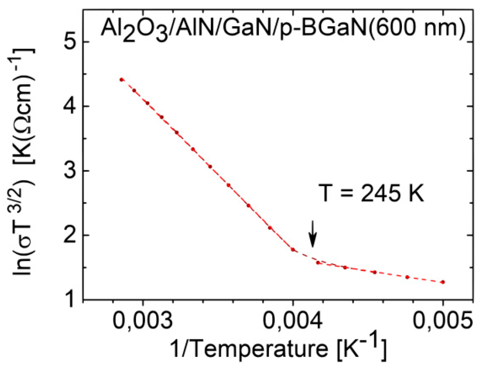
Figure 2.
Resistivity of p-BGaN layer as a function of Temperature at higher range.
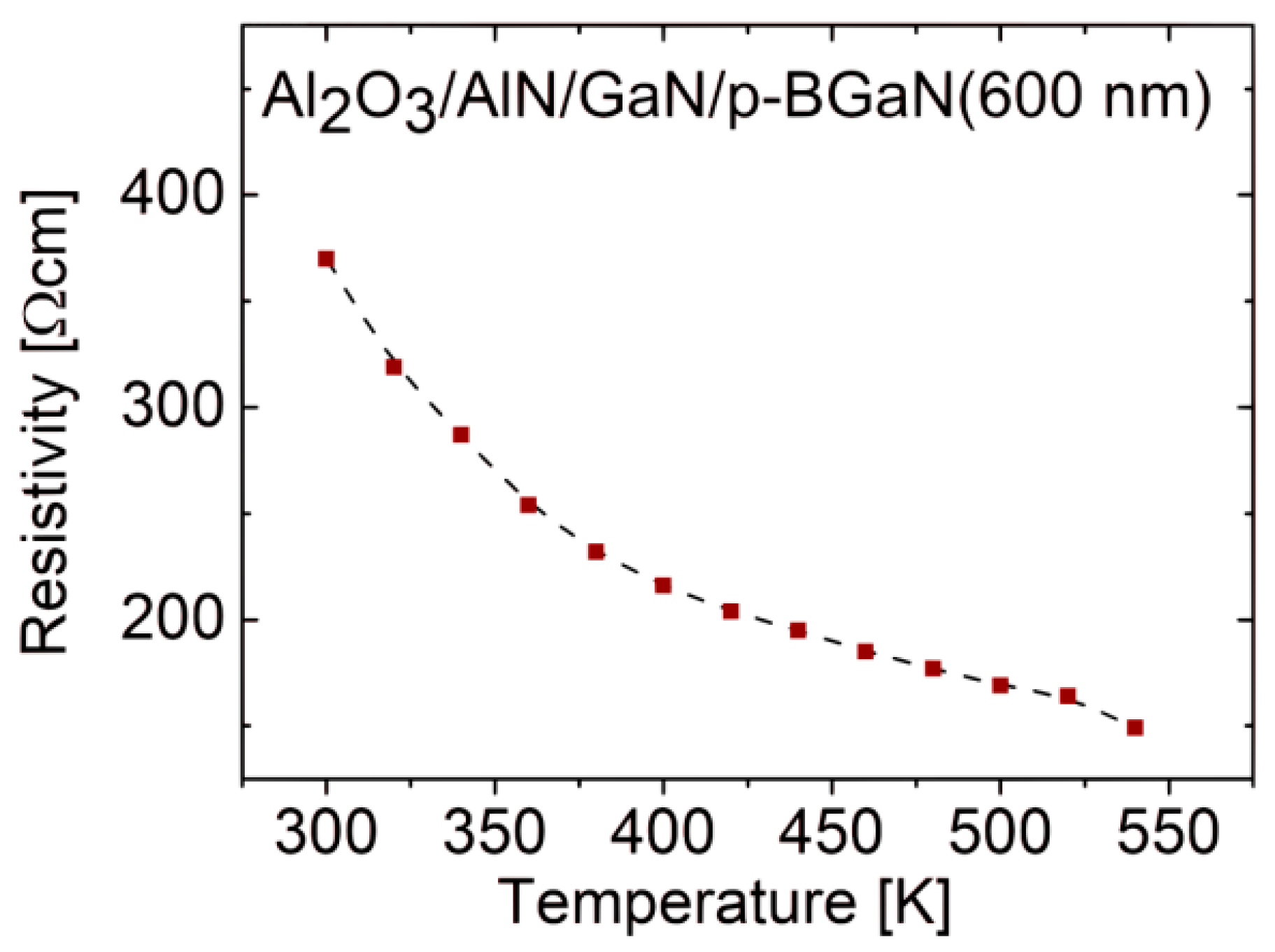
Figure 3.
Holes concentration nh as a function of Temperature.
Disclaimer/Publisher’s Note: The statements, opinions and data contained in all publications are solely those of the individual author(s) and contributor(s) and not of MDPI and/or the editor(s). MDPI and/or the editor(s) disclaim responsibility for any injury to people or property resulting from any ideas, methods, instructions or products referred to in the content. |
© 2025 by the authors. Licensee MDPI, Basel, Switzerland. This article is an open access article distributed under the terms and conditions of the Creative Commons Attribution (CC BY) license (http://creativecommons.org/licenses/by/4.0/).
Copyright: This open access article is published under a Creative Commons CC BY 4.0 license, which permit the free download, distribution, and reuse, provided that the author and preprint are cited in any reuse.


