Submitted:
10 June 2025
Posted:
10 June 2025
You are already at the latest version
Abstract
Diamond is an attractive substrate candidate for GaN high electron mobility transistor (HEMT) to enhance heat dissipation due to its exceptional thermal conductivity. However, the thermal boundary resistance (TBR) at the GaN-diamond interface poses a significant bottleneck to heat transport, exacerbating self-heating and limiting device performance. In this work, TCAD simulations were employed to systematically investigate the effects of thermal boundary layer (TBL) thickness (dTBL) and thermal conductivity (κTBL) on the electrothermal behavior of GaN-on-diamond HEMTs. Results show that increasing the TBL thickness (5–20 nm) or decreasing its thermal conductivity (0.1–1.0 W/(m·K)) leads to elevated hotspot temperatures and degraded electron mobility, resulting in notable deterioration of I-V characteristics. The nonlinear dependence of device performance on κTBL is attributed to Fourier’s law, where heat flux is inversely proportional to thermal resistance. Furthermore, co-analysis of substrate thermal conductivity and interfacial quality reveals that interface TBR has a more dominant impact on device behavior than substrate conductivity. Remarkably, devices with low thermal conductivity substrates and optimized interfaces can outperform those with high-conductivity substrates but poor interfacial conditions. These findings underscore the critical importance of interface engineering in thermal management of GaN-diamond HEMTs and provide a theoretical foundation for future work on phonon transport and defect-controlled thermal interfaces.
Keywords:
thermal boundary resistance
; heat transfer
; self-heating effects
; electron mobility degradation
; high electron mobility transistor
1. Introduction
Gallium nitride (GaN) has emerged as a leading material for fabricating high-performance transistors due to its wide bandgap, high saturation electron drift velocity, and superior breakdown characteristics[1,2]. Among GaN-based devices, the high electron mobility transistor (HEMT) is particularly attractive for high-power and high-frequency applications. However, under such operating conditions, localized thermal imbalance leads to an extremely high temperature at the hotspot, typically located between the drain and gate of the HEMT, causing a reduction in drain current[3]. This phenomenon known as the self-heating effect[4], imposes significant challenges on both performance and reliability GaN HEMT. Self-heating is critically linked to the Arrhenius dependence of the mean time to failure (MTTF) on temperature. Empirical data shows a 50% reduction in MTTF per 10-15 K increase under normal operating conditions[5,6]. Therefore, maintaining the hotspot temperature within a safe operating range, while maximizing output power density, has become a central focus in GaN device research[7]. Over the past few decades, several methods and techniques are proposed for device thermal management, including heat pipes, air cooling, phase change material cooling, thermoelectric cooling, etc. Among these, replacing the substrate with a material of higher thermal conductivity stands out as one of the most direct and effective approaches[8]. Conventional substrates for GaN, such as sapphire, SiC, and Si, offer thermal conductivities ranging from 40 to 400 W/(m·K), which limit the thermal performance of GaN devices. In contrast, diamond with a thermal conductivity exceeding 1800 W/(m·K) offers a compelling alternative, substantially enhancing the device thermal management[9], especially, currently industrial-scale diamond can be synthesized at reasonable cost[10].
However, despite diamond’s intrinsic thermal advantages, the overall heat dissipation efficiency of GaN-on-diamond structures is significantly influenced by the thermal boundary resistance (TBR) at the GaN-diamond interface. TBR is primarily attributed to several factors, including acoustic mismatch between GaN and diamond, dielectric interlayer used for diamond growth seeding, low-density damaged layer that forms on the diamond surface, and defective transition region near the diamond nucleation surface[11,12]. To address this challenge, several interface engineering approaches have been explored. Zhou attempted to directly grow diamond on GaN without spacers, aiming to achieve an ideal interface (TBR=3 m²·K/GW)[13,14]. However, interface degradation during diamond growth led to a significantly higher TBR of 61.1 m²·K/GW, and the resulting diamond layer exhibited a thermal conductivity of only 180 W/(m·K). In contrast, Zhou and Field introduced thin dielectric interlayers, such as 5 nm SiN, 5 nm AlN, and 10 nm SiC, as nucleation spacers. These configurations yielded TBR values of 6.5 m²·K/GW, 38.5 m²·K/GW, and 35 m²·K/GW respectively, while achieving diamond thermal conductivities of 500 W/(m·K), 900 W/(m·K), and 1500 W/(m·K) [15,16]. Additionally, Mu et al. employed the surface activated bonding (SAB) technique, which enables bonding GaN to bulk diamond at room temperature using a thin adhesion layer[17]. This method achieved a minimum TBR of 11 m²·K/GW, although it involves a complex fabrication process[18].
Based on these experimental insights, three critical parameters have been identified for accurate thermal modeling: interlayer thickness parameters, interlayer thermal conductivity, and substrate diamond thermal conductivity. To investigate the influence of GaN-diamond TBR on device characteristics, we conducted a comprehensive simulation study using Silvaco technology computer-aided design (TCAD) tools. By systematically varying the thermal and structural properties of the interface, we analyzed their effects on key performance metrics, including peak drain current, hotspot temperature, and electron mobility. Our findings provide a mechanistic understanding of TBR-governed self-heating in GaN HEMTs, offering design guidelines for improved thermal management. This work lays a theoretical framework for future studies of ballistic transport and interface-level energy dissipation phenomena in GaN-on-diamond systems.
2. Device Details and Simulation Methods
2.1. Device Model
The simulated GaN HEMT structure is illustrated in Figure 1. It consists of a SiN passivation layer, an Al0.25Ga0.75N barrier layer, a GaN buffer layer, a thermal boundary layer (TBL), and an underlying substrate. Among various GaN-on-diamond fabrication techniques, this study adopts direct epitaxial growth as the reference methodology, since it provides a more controllable and idealized interface, which is critical for evaluating thermal boundary resistance effects with minimal structural variability.
The detailed device parameters are listed in Table 1. The lateral dimension of the simulated GaN device is 10.4 µm, and the electrode thickness is set to 0.2 µm. The gate metal has a work function of 4.2 eV, forming a Schottky contact with the Al0.25Ga0.75N layer. It is important to note that the Schottky contact does not inject electrons but instead serves as an extraction point for high-energy electrons that acquire sufficient kinetic energy to surmount the potential barrier and reach the electrode[19]. This simply structure is an ideal choice for analyzing the underlying physics of electron transport and self-heating effects in GaN HEMT. Its moderate complexity enables detailed investigation of the interplay between thermal and electronic behavior, while maintaining computational feasibility for TCAD simulations.
2.2. Simulation Methodologies
In this work, the electronic and thermal characteristics of the GaN HEMT a were simulated using the Silvaco TCAD platform. This simulation environment incorporates a suite of advanced physical models that closely replicate real device behavior, enabling comprehensive analysis of both electrical and thermal performance[1]. The core of the simulation is based on solving the coupled Poisson equation and the carrier continuity equations under the drift-diffusion model, augmented by models for carrier statistics, collision ionization, carrier lifetime, mobility, and the generation-recombination process accurately.
Prior researches have shown that variations in the microstructure and properties of the TBL significantly influence the electrical characteristics of GaN-based devices[20]. However, the underlying mechanisms by which TBL parameters impact device performance remain inadequately understood. In this work, we adopt a bottom-up approach, that starts from macroscopic current-voltage characteristics, then progressively decouples and analyze the influences of individual microscopic parameters to elucidate these fundamental mechanisms. The electronic transport in the simulation is modeled using the drift-diffusion formalism derived from the Boltzmann transport equation. It is important to note that this derivation assumes that the validity of the Einstein relation, which links carrier mobility and diffusion coefficient[21]. The electron current density is obtained by:
where q is elementary charge, Dn is electron diffusivity dependent on temperature and mobility, n is electron concentration, μn is electron mobility, kB is Boltzmann constant, nie is effective intrinsic carrier concentration, and TL is lattice temperature.
Given that excessive heat generation is a primary reliability concern in GaN HEMTs, especially in the hotspot region between the gate and drain[22]. Therefore, accurate modeling of temperature distribution is essential. To address this problem, we incorporate the lattice heating model, which introduces the heat flow equation into the computational framework. Its general form is expressed as:
where C is heat capacity per unit volume, is thermal conductivity, H is heat generation rate, and TL is lattice temperature. The thermal conductivities employed in our simulations at room temperature (300 K) are summarized in Table 2.
Thermal conductivity in semiconductors is known to be temperature-dependent and follows a power law of the form[26]:
The L(300K) is thermal conductivity of materials at 300K.α is a quantitative parameter characterizing the temperature dependence of thermal conductivity (e.g., α = -0.28 for GaN)[27].
The accuracy of the temperature distribution simulations is critical for modeling localized hotspot and overall heat transfer process. Therefore, the heat exchange between the device and outside environment also should be considered carefully. Prior studies indicate that the impact of lateral heat dissipation through the device sidewalls is negligible[6,28]. Therefore, in our simulation, heat is assumed to be extracted only through the bottom Dirichlet boundary, while all other boundaries are set as adiabatic[29].
Equation (1) demonstrates the influence of electron mobility on current density, highlighting the necessity of accurate mobility models. Furthermore, considering the well-documented temperature dependence of electron mobility[30], we employ the temperature-dependent high-field/low-field mobility models (GANSAT and ALBRCT), ensuring high simulation fidelity[8,28].
The core objective of this work is to investigate how TBR at the GaN-diamond interface affects electrical performance, particularly current characteristics. Consequently, accurate modeling of TBR becomes critically important. Figure 2 illustrates the principal mechanisms responsible for TBR formation at GaN-diamond interface, including: 1) phonon scattering at the GaN-diamond interface; 2) scattering from defects, dislocations, and other imperfections within the transition layer; and 3) disorder-induced scattering near the interface region[13]. These three mechanisms hinder the phonon transmission across the interface, leading to increased TBR. Since phonons are the dominant heat carriers in semiconductors (with negligible contribution from electrons), only phonon-mediated heat transport is considered in this study[31].
To simulation TBR, TBL is introduced at the GaN-diamond interface[32]. The TBR is modeled using the relationship:
where dTBL is thickness of the thermal boundary layer and κTBL is thermal conductivity of the TBL. This approach enables us to precisely investigate the impact of interfacial heat transfer resistance on the thermal and electrical behavior of GaN-on-diamond HEMTs.
3. Simulation Results and Discussion
3.1. Effect of Thermal Boundary Layer Thickness
Experimental studies have revealed that during the direct growth of GaN-on-diamond, ion flux excitation can induce atomic interdiffusion and interfacial amorphization, which significantly affects interfacial heat transport[17,18]. Based on experimentally observed diffusion thicknesses in the range of 5-20 nm and measured TBR values between 12.5 and 50 m²·K/GW, the thermal conductivity of the TBL in the simulations is set to κTBL=0.4 W/(m·K), in accordance with Equation (4).
As shown in Figure 3(a), increasing the dTBL results in a clear degradation in electrical performance. Especially, the peak drain current decreases from 0.723 A to 0.608 A as dTBL increases from 5 nm to 20 nm, corresponding to relative reduction of 4.98%, 5.95%, and 4.98% across incremental thicknesses, respectively. This trend is consistent with the literature, which identifies excessive self-heating, particularly in hotspot regions, as a primary degradation mechanism in GaN HEMT[22]. The relationship between peak hotspot temperature and drain voltage is shown in Figure 3(b). The hotspot temperature of device increases linearly with the increase of drain voltage, and the peak temperature rises from 414 K to 431 K with the increasing dTBL. Figure 3(c) and 3(d) illustrate the spatial temperature distribution for TBL thicknesses of 5 nm and 20 nm, respectively. A thicker TBL results in a significantly higher localized temperature, particularly around the hotspot region.
Figure 3(e) presents the vertical temperature distribution within the device (horizontally located at 7 µm), traversing the channel. The central hotspot exhibits a relatively flat and elevated temperature plateau, indicative of substantial heat accumulation. Simultaneously, the lattice temperature decreases with the increase of distance from the hot spot, and the decreasing trend of lattice temperature tends to be flat with the increase of distance, indicating that enhanced thermal conduction in the GaN with the decrease of temperature. Notably, when the dTBL increases from 5 nm to 20 nm, the interfacial temperature difference rises from 22.3 K to 63.6 K. This confirms that increased dTBL inhibits thermal transport across GaN-diamond interface, exacerbating local heating.
As described by Equation (1), electron mobility is a critical factor directly governing current density. Figure 3(f) demonstrates that the peak electron mobility in the channel layer decreases linearly from 858 cm²/(V·s) to 757 cm²/(V·s) with increasing dTBL. This trend aligns well with temperature-dependent Hall effect measurements, which demonstrate that elevated temperatures enhance phonon activity and consequently increase phonon scattering rates and reduce carrier mobility [33,34].
The simulation results offer insight into the underlying mechanisms through which dTBL affects device characteristics. As the dTBL increases, phonons experience extended transport paths and are more likely to scatter with interfacial defects, impurities, or amorphous structures. Moreover, increased TBL thickness is typically associated with a higher degree of interfacial disorder, further impeding phonon transmission.
These phenomena are captured in the simulations through an equivalent TBR, which effectively suppresses interfacial heat transfer. The resulting heat accumulation elevates the temperature of the GaN channel, which in turn reduces the material’s thermal conductivity, creating a positive feedback loop that further impedes heat dissipation and exacerbates hotspot formation.
Ultimately, elevated temperatures in the two-dimensional electron gas (2DEG) channel reduce electron mobility, resulting in the deterioration of the device’s electrical performance. These findings highlight the critical role of interfacial thermal engineering in the design and optimization of GaN-on-diamond HEMTs.
3.2. Effect of Thermal Boundary Layer Thermal Conductivity
During the GaN-on-diamond fabrication process, ion beam-induced damage near the interface introducing a high defect density, including dislocations and vacancies. These defects substantially reduce the local thermal conductivity compared to the bulk material, with the extent of degradation strongly dependent on processing parameters. To investigate the influence of κTBL on device performance, a systematic parameter sweep was conducted across a TBR range of 5-50 m²·K/GW, derived from simulation data. A dTBL was fixed at 5 nm in the simulations to effectively isolate the effects of κTBL from those of layer thickness, thereby enabling a focused analysis of κTBL’s impact on the device’s electrical performance.
As shown in Figure 4(a), κTBL significantly affects the peak drain current. When the κTBL is 1 W/(m·K), the peak current reaches 0.733 A. However, when κTBL decreases to 0.1 W/(m·K), the peak current drops to 0.629 A, a reduction of approximately 14.1%. This decline is attributed to intensified self-heating, which limits carrier mobility and current conduction. As shown in Figure 4(b), the hotspot peak temperature increases significantly as κTBL decreases. Specifically, for κTBL=1 W/(m·K), the hotspot peak temperature reaches 391.1 K, while the κTBL=0.1 W/(m·K), it rises to 445.7 K. Notably, a nonlinear trend is observed: reducing κTBL from 1 W/(m·K) to 0.5 W/(m·K) increases the hotspot peak temperature by only 9.1 K (2.3%), whereas a further reduction to 0.1 W/(m·K) results in a sharp 45.5K rise (11.6%). This suggests a threshold behavior where thermal transport begins to degrade rapidly below a certain κTBL.
Figure 4(c) and (d) depict the spatial temperature distributions for κTBL =0.1 and 1 W/(m·K), respectively. The lower κTBL case shows significantly higher overall temperatures, especially in hotspot regions, indicating inefficient heat dissipation.
Figure 4(e) presents the vertical temperature profile of the device, revealing that the interfacial temperature jump also exhibits pronounced nonlinearity. For κTBL=1 W/(m·K), the temperature jump at the interface is 9.3 K, which increases to 72.6K when the κTBL drops to 0.1 W/(m·K). Notably, the decrease from 1 W/(m·K) to 0.5 W/(m·K) causes only an 8.3 K rise (89.2%), whereas the decrease from 0.5 W/(m·K) to 0.1 W/(m·K) results in a dramatic 55 K rise (591.3%). These findings further emphasize the critical importance of maintaining adequate interfacial thermal conductivity for effective heat dissipation.
Figure 4(f) shows the relationship between κTBL and electron mobility in the 2DEG channel. The electron mobility exhibits a sharp decline when the κTBL below 0.4 W/(m·K), highlighting a threshold behavior. This abrupt change suggests that reduced thermal transport at the interface significantly impacts phonon dynamics, increasing phonon scattering and thereby limiting carrier mobility. When plotted as TBR versus mobility (inset), a linear relationship emerges, consistent with expectations from heat transfer theory. According to Fourier’s law, the thermal resistances in series is analogous to the series model of electrical resistances, whereas the use of thermal conductance requires reciprocal processing.
In the simulations, a TBL is placed between two thermal conductors. Heat flux across the interface is calculated as:
Since TBR is defined as Equation (4), the inverse relationship between κTBL and TBR leads to the observed nonlinear dependence of mobility on κTBL, despite the linearity between mobility and TBR.
Based on the aforementioned analysis, reductions in κTBL stem primarily from bombardment-induced defect accumulation at the interface, which enhances phonon scattering. The phonon mean free path is shortened during thermal transport and thus raising the effective TBR. These effects impede heat exchange between GaN and diamond, resulting in elevated hotspot temperatures and degraded carrier transport, mirroring the performance deterioration previously described for increased TBL thickness.
3.3. Effect Substrate and Thermal Boundary Layer Thermal Conductivity
Experimental observations have shown that even under identical interface conditions, the thermal conductivity of diamond substrates grown by different methods can vary significantly. In particular, poor crystalline quality and defect-rich diamond films may exhibit thermal conductivities as low as 100 W/(m·K), far below the ideal bulk value[22,35]. To evaluate the combined influence of the diamond substrate and TBL on device behavior, simulations were conducted under identical interfacial conditions using both high (1500 W/(m·K)) and low (100 W/(m·K)) thermal conductivity diamond substrates. This approach enabled a comparative analysis of device characteristics under varying substrate qualities and interfacial scenarios.
The I-V characteristics of devices with high thermal conductivity and low thermal conductivity diamond substrates under varying κTBL values are shown in Figure 5(a). When the κTBL decreased from 0.9 W/(m·K) to 0.1 W/(m·K), the peak drain current of HEMT devices with high thermal conductivity diamond substrates dropped by 0.099 A (13.6%) due to pronounced self-heating effects, while the corresponding current reduction with low thermal conductivity substrates (100 W/(m·K)) is only 0.02 A (3.34%). This significant difference indicates that devices with high thermal conductivity diamond substrates are more sensitive to changes in interfacial thermal resistance. Even minor increases in interfacial thermal resistance can result in substantial performance degradation, whereas devices with inherently poor heat dissipation (low κd) display a relatively muted response to such variations.
Figure 5(b) reveals that the peak hot spot temperature increased by 44.3 K (11%) in high κd devices and by 53.7 K (13.6%) in low κd devices when the κTBL changed from 0.9 W/(m·K) to 0.1 W/(m·K). Interestingly, as shown in Figs. 5(c) and (d), both device types exhibit similar temperature distributions when κTBL=0.1 W/(m·K), despite their vastly different substantial substrate thermal conductivity. This suggests that, under severe interfacial thermal resistance conditions, the substrate’s intrinsic thermal conductivity becomes secondary to the bottleneck imposed by the TBL. Figure 5(e) further supports this observation by illustrating nearly identical vertical temperature profiles in both devices, confirming that interfacial thermal resistance dominates overall heat transport. These findings imply that the TBL imposes comparable suppression of heat flow in both high- and low-conductivity substrates. However, the operational consequences differ: in high-κd devices, the degradation is more dramatic because they are transitioning from an initially high-performance state. Conversely, devices with low κd substrates operate from the outset in a limited thermal regime and thus experience smaller performance deltas in response to interfacial degradation. These findings are consistent with previous studies on the effects of substrate materials in device reliability and efficiency[28,36]. Figure 5(f) shows that electron mobility decreases with increasing TBR for both substrate types, consistent with earlier analyses of κTBL-dependent mobility. Notably, in devices with high κd substrates, a sufficiently poor κTBL causes the electron mobility to degrade to the level that of low κd devices that possess superior interfacial thermal properties. This degradation is also reflected in current output: under severely degraded interface conditions, devices with excellent bulk thermal substrates may underperform relative to those built on poorer substrates with better interface quality.
These findings underscore the critical importance of optimizing not only the substrate material but also the quality of the GaN-diamond interface. Even with high-κd diamond, poor interfacial thermal transport can negate the substrate’s advantages and significantly impair device performance.
4. Summary and Conclusions
This study systematically investigated the thermal management challenges in diamond-based GaN HEMT through comprehensive TCAD simulations, with particularly focus on the interfacial TBR at the GaN-diamond interface. Although diamond substrates with high intrinsic thermal conductivity offer exceptional heat dissipation potential, their effectiveness is often compromised by interfacial imperfections, which introduce substantial TBR and severely limit heat flow, thereby exacerbating the device self-heating effect. By varying the thickness of the TBL, it was demonstrated that increased interface thickness significantly elevates the hotspot temperature and reduces electron mobility, resulting in degraded output characteristics. Similarly, adjusting the TBL thermal conductivity κTBL revealed that lower conductivity layers induce a steep rise in hotspot temperature and a notable decline in electron mobility. This degradation in device performance arises from the non-linear dependence between κTBL and electron mobility, governed by Fourier’s law and the inverse relationship between heat flux density and thermal resistance. Furthermore, a comparative analysis between high- and low-thermal-conductivity diamond substrates under identical interfacial conditions highlighted that high-κd substrates are substantially more sensitive to TBR variations. Under severe interface degradation, devices with high-κd diamond showed a 13.6% reduction in peak current, whereas those with low-κd diamond exhibited only a 3.34% reduction. Crucially, the simulations revealed a counterintuitive result: devices with optimized interfaces on low-κd substrates can outperform those with high-κd substrates suffering from poor interfacial quality. This finding underscores the dominant role of interface engineering over substrate thermal conductivity in achieving optimal device performance.
The insights from this work provide valuable reference data, including temperature field distributions, electron mobility profiles, and interfacial transport parameters, that can be directly utilized in microscale modeling of GaN–diamond systems. Moreover, these results establish a theoretical foundation for future studies on ballistic phonon transport, interfacial defect dynamics, and advanced thermal management strategies. Overall, this work advances the understanding of thermal transport bottlenecks in GaN-on-diamond devices and offers practical guidance for interface optimization in next-generation high-power electronics.
Acknowledgements
The authors gratefully acknowledge the financial support from National Natural Science Foundation of China (Grant Nos. 12374027, 52206080, 12304039, and 52306102), the Shanghai Committee of Science and Technology (Grant No. 21TS1401500).
References
- Chang, C.-Y.; Douglas, E.; Kim, J.; Lu, L.; Lo, C.-F.; Chu, B.-H.; Cheney, D.; Gila, B.P.; Ren, F.; Via, G. Electric-field-driven degradation in off-state step-stressed AlGaN/GaN high-electron mobility transistors. IEEE Transactions on Device and Materials reliability 2011, 11, 187–193. [Google Scholar] [CrossRef]
- Nigam, A.; Bhat, T.N.; Rajamani, S.; Dolmanan, S.B.; Tripathy, S.; Kumar, M. Effect of self-heating on electrical characteristics of AlGaN/GaN HEMT on Si (111) substrate. AIP Advances 2017, 7, 085015. [Google Scholar] [CrossRef]
- Hu, B.; Wang, Z.; Xu, K.; Tang, D. Hotspot and nonequilibrium thermal transport in AlGaN/GaN FinFET: A coupled electron-phonon Monte Carlo simulation study. International Journal of Heat and Mass Transfer 2025, 241, 126679. [Google Scholar] [CrossRef]
- Chang, Y.; Zhang, Y.; Zhang, Y.; Tong, K. A thermal model for static current characteristics of AlGaN∕ GaN high electron mobility transistors including self-heating effect. Journal of applied physics 2006, 99, 044501. [Google Scholar] [CrossRef]
- Lee, S.; Vetury, R.; Brown, J.D.; Gibb, S.R.; Cai, W.Z.; Sun, J.; Green, D.S.; Shealy, J. In Reliability assessment of AlGaN/GaN HEMT technology on SiC for 48V applications, 2008 IEEE International Reliability Physics Symposium, 2008; IEEE: pp 446-449.
- Wang, A.; Tadjer, M.; Calle, F. Simulation of thermal management in AlGaN/GaN HEMTs with integrated diamond heat spreaders. Semiconductor science and technology 2013, 28, 055010. [Google Scholar] [CrossRef]
- Pomeroy, J.W.; Bernardoni, M.; Dumka, D.; Fanning, D.; Kuball, M. Low thermal resistance GaN-on-diamond transistors characterized by three-dimensional Raman thermography mapping. Applied Physics Letters 2014, 104, 083513. [Google Scholar] [CrossRef]
- Tang, D.-S.; Cao, B.-Y. Phonon thermal transport and its tunability in GaN for near-junction thermal management of electronics: A review. International Journal of Heat and Mass Transfer 2023, 200, 123497. [Google Scholar] [CrossRef]
- Francis, D.; Faili, F.; Babić, D.; Ejeckam, F.; Nurmikko, A.; Maris, H. Formation and characterization of 4-inch GaN-on-diamond substrates. Diamond and Related Materials 2010, 19, 229–233. [Google Scholar] [CrossRef]
- Yahya, N.; Nor, R.M.; Bakar, S.A.; Thandavan, T.M.; Rusop, M. Diamond: synthesis, characterisation and applications. Carbon and Oxide Nanostructures: Synthesis, Characterisation and Applications, 2011; 195–217. [Google Scholar]
- Sun, H.; Simon, R.B.; Pomeroy, J.W.; Francis, D.; Faili, F.; Twitchen, D.J.; Kuball, M. Reducing GaN-on-diamond interfacial thermal resistance for high power transistor applications. Applied Physics Letters 2015, 106, 111906. [Google Scholar] [CrossRef]
- Okamoto, N.; Minoura, Y.; Sato, M.; Ohki, T.; Ozaki, S.; Makiyama, K.; Yamada, A.; Kotani, J.; Joshin, K.; Nakamura, N. Thermal analysis of GaN-HEMT/SiC on diamond by surface activated bonding. Diamond 2018, 1, 75–78. [Google Scholar]
- Zhou, Y.; Anaya, J.; Pomeroy, J.; Sun, H.; Gu, X.; Xie, A.; Beam, E.; Becker, M.; Grotjohn, T.A.; Lee, C. Barrier-layer optimization for enhanced GaN-on-diamond device cooling. ACS applied materials & interfaces 2017, 9, 34416–34422. [Google Scholar]
- Won, Y.; Cho, J.; Agonafer, D.; Asheghi, M.; Goodson, K.E. Fundamental cooling limits for high power density gallium nitride electronics. IEEE transactions on components, Packaging and Manufacturing Technology 2015, 5, 737–744. [Google Scholar]
- Jia, X.; Wei, J. j.; Kong, Y.; Li, C. m.; Liu, J.; Chen, L.; Sun, F.; Wang, X. The influence of dielectric layer on the thermal boundary resistance of GaN-on-diamond substrate. Surface and Interface Analysis 2019, 51, 783–790. [Google Scholar] [CrossRef]
- Field, D.E.; Cuenca, J.A.; Smith, M.; Fairclough, S.M.; Massabuau, F.C.; Pomeroy, J.W.; Williams, O.; Oliver, R.A.; Thayne, I.; Kuball, M. Crystalline interlayers for reducing the effective thermal boundary resistance in GaN-on-diamond. ACS Applied Materials & Interfaces 2020, 12, 54138–54145. [Google Scholar]
- Mu, F.; He, R.; Suga, T. Room temperature GaN-diamond bonding for high-power GaN-on-diamond devices. Scripta Materialia 2018, 150, 148–151. [Google Scholar] [CrossRef]
- Cheng, Z.; Mu, F.; Yates, L.; Suga, T.; Graham, S. Interfacial thermal conductance across room-temperature-bonded GaN/diamond interfaces for GaN-on-diamond devices. ACS applied materials & interfaces 2020, 12, 8376–8384. [Google Scholar]
- Hasegawa, H.; Akazawa, M. Current Transport, Fermi Level Pinning, and Transient Behavior\ofGroup-III Nitride Schottky Barriers. Journal of the Korean Physical Society 2009, 55, 1167–1179. [Google Scholar] [CrossRef]
- Zhang, G.; Zhao, M.; Yan, C.; Sun, B.; Wu, Z.; Chang, H.; Jin, Z.; Sun, J.; Liu, H. Thermal analysis of AlGaN/GaN high-electron-mobility transistors with graphene. Journal of Nanoscience and Nanotechnology 2018, 18, 7578–7583. [Google Scholar] [CrossRef]
- Selberherr, S. Analysis and simulation of semiconductor devices. Springer Science & Business Media: 2012.
- Meneghini, M.; Rossetto, I.; De Santi, C.; Rampazzo, F.; Tajalli, A.; Barbato, A.; Ruzzarin, M.; Borga, M.; Canato, E.; Zanoni, E. In Reliability and failure analysis in power GaN-HEMTs: An overview, 2017 IEEE International Reliability Physics Symposium (IRPS), 2017; IEEE: pp 3B-2.1-3B-2.8.
- Piprek, J. Semiconductor optoelectronic devices: introduction to physics and simulation. Elsevier: 2013.
- Mendes, J.C.; Liehr, M.; Li, C. Diamond/GaN HEMTs: where from and where to? Materials 2022, 15, 415. [Google Scholar] [CrossRef]
- Liu, D.; Fabes, S.; Li, B.-S.; Francis, D.; Ritchie, R.O.; Kuball, M. Characterization of the interfacial toughness in a novel “GaN-on-diamond” material for high-power RF devices. ACS Applied Electronic Materials 2019, 1, 354–369. [Google Scholar] [CrossRef]
- Das, S.K.; Putra, N.; Thiesen, P.; Roetzel, W. Temperature dependence of thermal conductivity enhancement for nanofluids. J. Heat Transfer 2003, 125, 567–574. [Google Scholar] [CrossRef]
- Zheng, Q.; Li, C.; Rai, A.; Leach, J.H.; Broido, D.A.; Cahill, D.G. Thermal conductivity of GaN, GaN 71, and SiC from 150 K to 850 K. Physical Review Materials 2019, 3, 014601. [Google Scholar] [CrossRef]
- Wang, K.; Hu, W.; Wu, S.; Wang, H.; Padhiar, M.A.; Ji, Y. Simulation investigation of effects of substrate and thermal boundary resistance on performances of AlGaN/GaN HEMTs. Physica Scripta 2024, 99, 065554. [Google Scholar] [CrossRef]
- Deng, X.; Zhang, B.; Li, Z. Electro-thermal analytical model and simulation of the self-heating effects in multi-finger 4H-SiC power MESFETs. Semiconductor science and technology 2007, 22, 1339. [Google Scholar] [CrossRef]
- Li, S.S.; Thurber, W.R. The dopant density and temperature dependence of electron mobility and resistivity in n-type silicon. Solid-State Electronics 1977, 20, 609–616. [Google Scholar] [CrossRef]
- Mahalingam, M. Thermal management in semiconductor device packaging. Proceedings of the IEEE 1985, 73, 1396–1404. [Google Scholar] [CrossRef]
- Adnan, K.Z.; Feng, T. Thermal boundary conductance and thermal conductivity strongly depend on nearby environment. Physical Review B 2024, 109, 245302. [Google Scholar] [CrossRef]
- Ko, T.-S.; Lin, D.-Y.; Lin, C.-F.; Chang, C.-W.; Zhang, J.-C.; Tu, S.-J. High-temperature carrier density and mobility enhancements in AlGaN/GaN HEMT using AlN spacer layer. Journal of Crystal Growth 2017, 464, 175–179. [Google Scholar] [CrossRef]
- Neamen, D.A. Semiconductor physics and devices: basic principles. 2003. McGraw-hill.
- Zhou, Y.; Ramaneti, R.; Anaya, J.; Korneychuk, S.; Derluyn, J.; Sun, H.; Pomeroy, J.; Verbeeck, J.; Haenen, K.; Kuball, M. Thermal characterization of polycrystalline diamond thin film heat spreaders grown on GaN HEMTs. Applied Physics Letters 2017, 111, 041901. [Google Scholar] [CrossRef]
- García, S.; Íñiguez-de-la-Torre, I.; Mateos, J.; González, T.; Pérez, S. Impact of substrate and thermal boundary resistance on the performance of AlGaN/GaN HEMTs analyzed by means of electro-thermal Monte Carlo simulations. Semiconductor Science and Technology 2016, 31, 065005. [Google Scholar] [CrossRef]
Figure 1.
Schematic model of GaN HEMT structure.
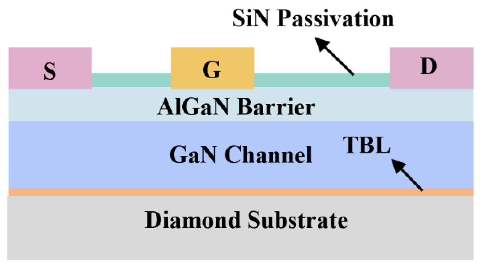
Figure 2.
Mechanisms contributing to thermal boundary resistances between at the GaN-diamond interface.
Figure 2.
Mechanisms contributing to thermal boundary resistances between at the GaN-diamond interface.
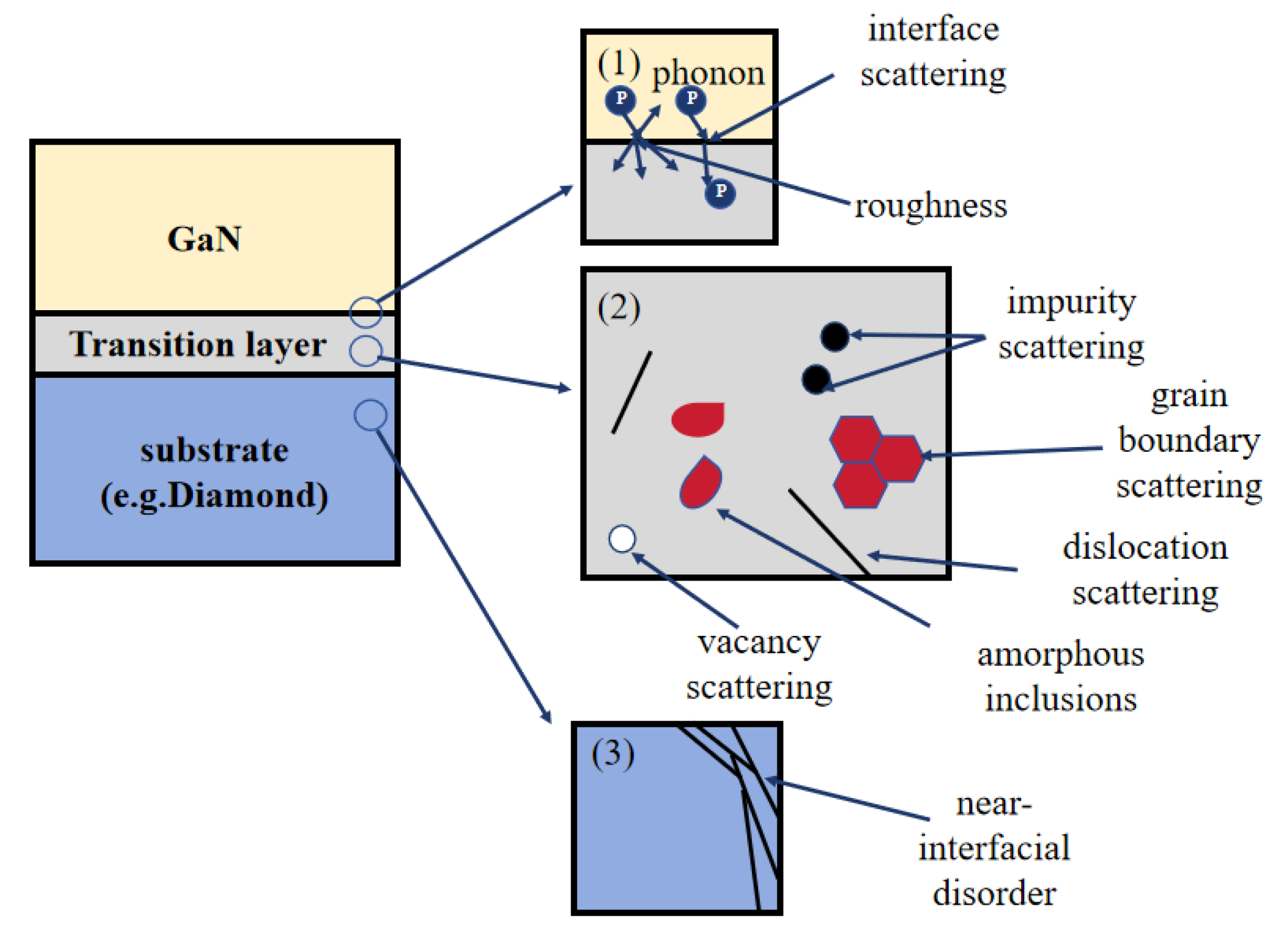
Figure 3.
(a) Drain I-V characteristics. (b) Relationship between hotspot peak temperature and drain voltage. (c) Temperature distribution of device with 5 nm dTBL. (d) Temperature distribution of device with 20 nm dTBL. (e) Vertical temperature profile of GaN HEMT. (f) Electron mobility versus dTBL.
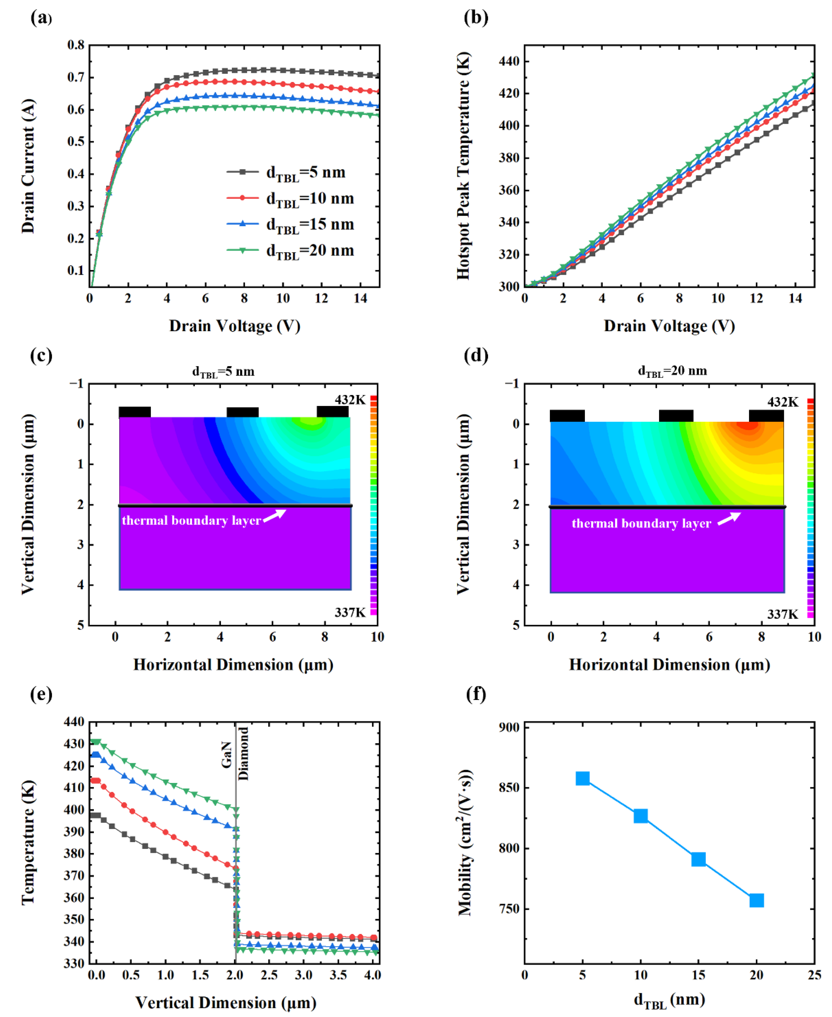
Figure 4.
(a) Drain current-voltage (I-V) characteristic curves. (b) Correlation between hotspot peak temperature and drain voltage. (c) Temperature field distribution of the device with the κTBL is 0.1 W/(m·K). (d) Temperature distribution in the device with κTBL=1 W/(m·K). (e) Vertical temperature profile in GaN HEMT. (f) Electron mobility versus κTBL (with inset illustrating the TBR-mobility relationship).
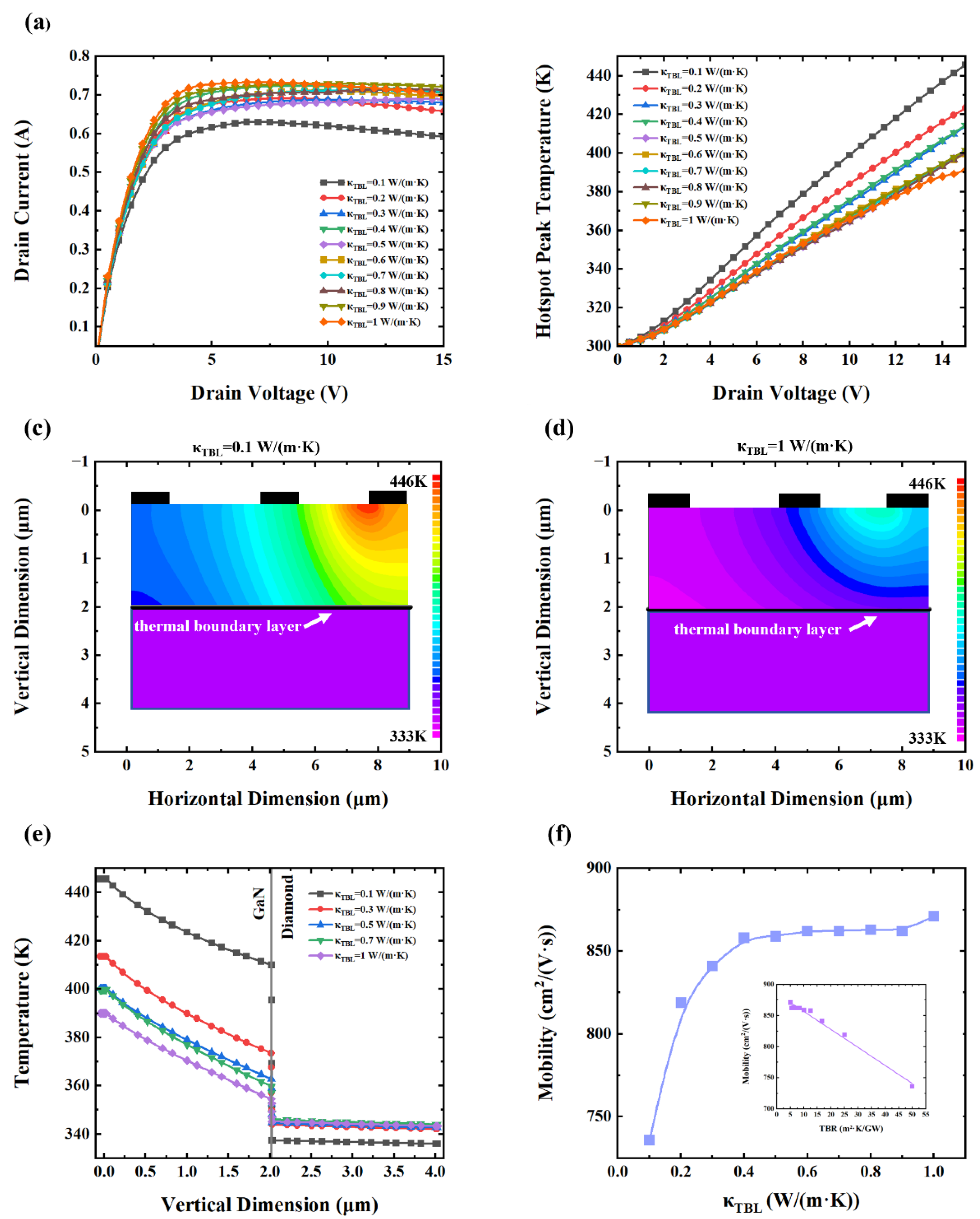
Figure 5.
(a) Drain current-voltage (I-V) characteristics. (b) Correlation between hotspot peak temperature and drain voltage. (c) Temperature distribution of device with the diamond thermal conductivity κd=1500 W/(m·K) and κTBL=0.1 W/(m·K). (d) Temperature field distribution of device with κd=100 W/(m·K) and κTBL=0.1 W/(m·K). (e) Vertical temperature profile in GaN HEMT. (f) Electron mobility versus TBR layer conductivity.
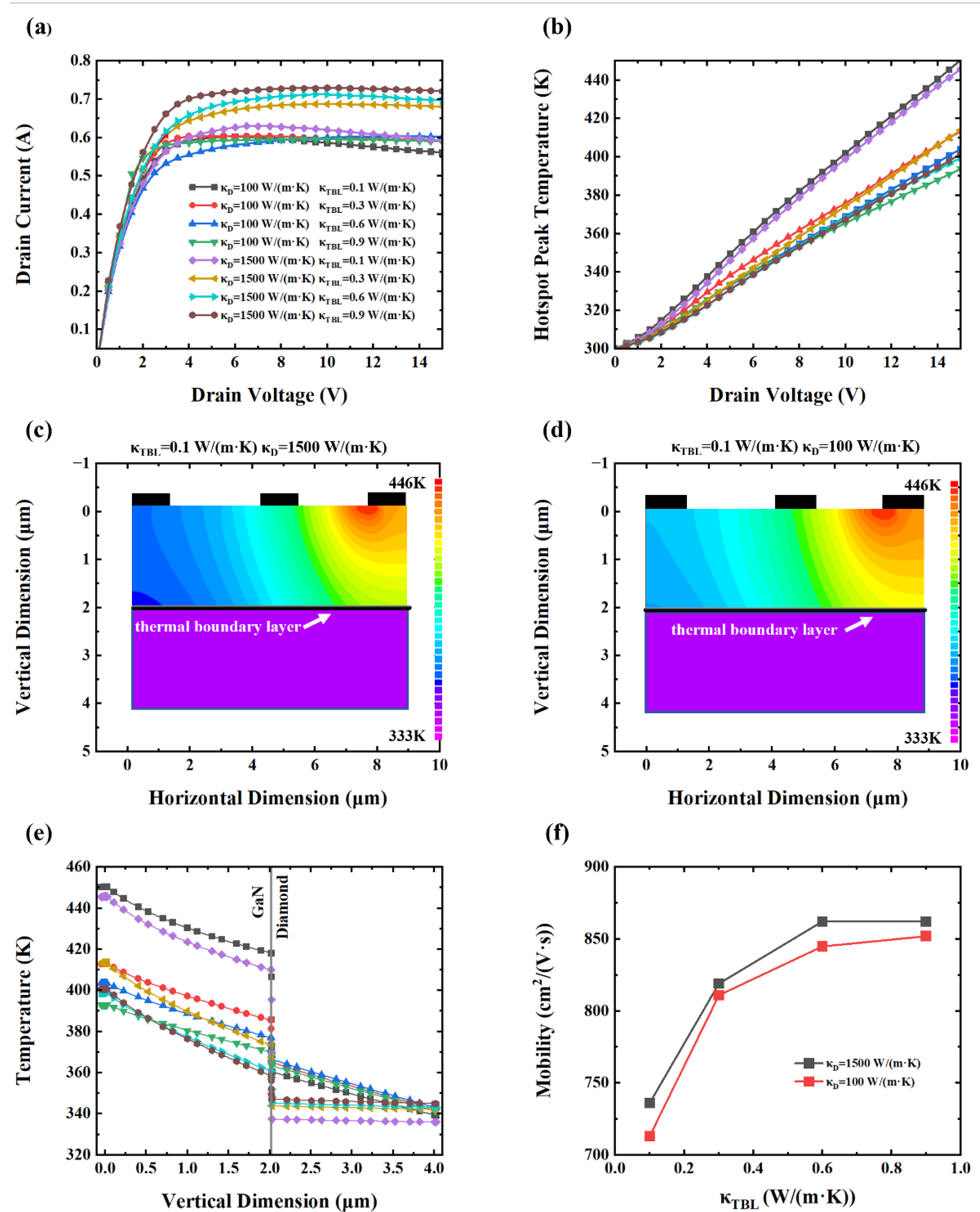

Table 1.
The geometrical parameters of the model.
| Parameter | Value |
| Al0.25Ga0.75N barrier layer thickness | 20 nm |
| GaN buffer layer thickness | 2 µm |
| Thermal boundary layer thickness | 5 nm (unless stated otherwise) |
| Diamond substrate thickness | 2 µm |
| SiN passivation thickness | 50 nm |
| Source length (Ls) | 1µm |
| Gate length (Lg) | 1.4 µm |
| Drain length (Ld) | 1 µm |
| Source to gate channel length (Lsg) | 1 µm |
| Gate to drain channel length (Lgd) | 6 µm |
Disclaimer/Publisher’s Note: The statements, opinions and data contained in all publications are solely those of the individual author(s) and contributor(s) and not of MDPI and/or the editor(s). MDPI and/or the editor(s) disclaim responsibility for any injury to people or property resulting from any ideas, methods, instructions or products referred to in the content. |
© 2025 by the authors. Licensee MDPI, Basel, Switzerland. This article is an open access article distributed under the terms and conditions of the Creative Commons Attribution (CC BY) license (http://creativecommons.org/licenses/by/4.0/).
Copyright: This open access article is published under a Creative Commons CC BY 4.0 license, which permit the free download, distribution, and reuse, provided that the author and preprint are cited in any reuse.


