Submitted:
24 October 2024
Posted:
25 October 2024
You are already at the latest version
Abstract
As the demand for high-frequency and high-power electronic devices has increased, gallium nitride (GaN), particularly in the context of high electron mobility transistors (HEMTs), has attracted considerable attention. However, the ‘self-heating effect' of GaN HEMTs represents a significant limitation in terms of both performance and reliability. Diamond, renowned for its exceptional thermal conductivity, represents an optimal material for the enhancement of thermal management in HEMTs. This paper puts forward a novel method for directly depositing diamond films onto N-polar GaN (NP-GaN) epitaxial layers. This eliminates the complexities of the traditional diamond growth process and the need for temporary substrate steps. Given the relative lag in N-polar material growth technologies, which are marked by surface roughness issues, and the recognition that the thermal boundary resistance (TBRGaN/diamond) represents a critical factor constraining efficient heat transfer, our study introduced a series of optimisations with the objective of enhancing the quality of the diamond nucleation layer while ensuring that the integrity of the GaN buffer layer remains intact. Moreover, chemical mechanical polishing (CMP) technology was employed to effectively reduce the surface roughness of the NP-GaN base, thereby providing a more favourable foundation for diamond growth. The optimisation trends observed in the thermal performance test results were encouraging. The integration of diamond films onto highly smooth NP-GaN epitaxial layers demonstrated a reduction in TBRGaN/Diamond compared to diamond layers deposited onto NP-GaN with higher surface roughness that had undergone no prior process treatment.
Keywords:
GaN HEMT
; self-heating effect
; NP-GaN
; GaN-on-diamond
; TBR
1. Introduction
In recent years, there has been a notable increase in the demand for electronic devices capable of operating at high frequencies and power. GaN, a third-generation semiconductor material that follows silicon (Si) and gallium arsenide (GaAs), has attracted considerable research interest due to its exceptional properties, including a wide bandgap and high breakdown electric field strength. It is noteworthy that GaN HEMTs, which utilize the polarization effect within the AlGaN/GaN heterojunction to generate a two-dimensional electron gas (2DEG), exhibit remarkable carrier densities approaching 1013 cm-2 and mobilities spanning 1800-2300 cm2/(V·s). These attributes serve to enhance both the operating voltage and frequency[1,2]. However, this performance advancement is accompanied by a pronounced 'self-heating effect', which has a detrimental impact on performance and reliability[3,4,5]. To address this challenge and fully realize the potential of GaN HEMTs, effective thermal management strategies have become a crucial consideration. While traditional passive methods offer certain benefits, they are constrained by size, weight, and power consumption (SWaP) considerations. In contrast, active thermal management techniques make use of high-κ materials to enhance the transfer of heat within the near-junction region of the device, thereby improving the efficiency of heat dissipation. This approach allows for the attainment of higher power densities while simultaneously reducing the dimensions of the device. Among the numerous materials that have been investigated, diamond is an exceptionally promising candidate for enhancing the thermal performance of HEMTs. Its unparalleled κ, exceeding 1800 W/m·K even in a polycrystalline form, coupled with its excellent insulating properties, renders it markedly superior to conventional materials, such as sapphire, Si, and silicon carbide (SiC)[6].
The chemical vapor deposition (CVD) of polycrystalline diamond (PCD) on GaN represents a relatively mature technology in the integration of GaN and diamond. Its distinctive advantage lies in the ability to deposit materials on a large area. However, the prevailing diamond-on-GaN growth process frequently necessitates intricate pre-processing stages, particularly the prerequisite of bonding the GaN front side to a temporary substrate. This step provides structural support during the deposition of diamond films on the back side, subsequent to the removal of the original substrate[7]. This methodology inevitably gives rise to technical challenges in terms of bonding and stripping, which may result in the introduction of additional stresses and residual surface defects on the GaN surface. This, in turn, may compromise the stability and reliability of the final device, particularly given that the HEMT is essentially a surface device. An alternative methodology entails the direct utilization of a back-side-up epitaxial wafer (NP-GaN) as the growth base. This eliminates the necessity for a temporary substrate, simplifies the process flow (as illustrated in Figure 1), and enables the direct deposition of diamond on NP-GaN. However, the technological capabilities for the growth of N-polar materials are significantly less advanced than those for Ga-polar materials, which are more prevalent. The primary challenge arises from the generally inferior quality of N-polar Group III nitride materials produced under current technological conditions, particularly surface roughness issues, such as the proliferation of hexagonal defects on the surface of NP-GaN films heteroepitaxially grown on orthorhombic sapphire or C-face SiC (C-SiC) substrates[8,9,10]. These defects persist even during GaN homoepitaxy, severely limiting their potential applications[11]. Moreover, irrespective of whether diamond is grown on Ga-polar GaN (GaP-GaN) or NP-GaN bases, TBRGaN/diamond represents a significant obstacle to efficient heat conduction from the active region to the diamond layer[12]. The TBRGaN/diamond is predominantly contingent upon the low-κ dielectric layer, which serves to protect the GaN layer[13]. Furthermore, the issue is compounded by the low quality of the diamond nucleation layer and poor interface quality[14]. Therefore, although the direct deposition of diamond on NP-GaN considerably simplifies the process, the compromised surface quality of NP-GaN is likely to have a significant negative impact on TBRGaN/diamond, ultimately limiting the overall thermal management performance.
In response to the aforementioned issues, we conducted experimental investigations with the objective of minimizing TBRGaN/diamond. This was achieved by employing microwave-plasma chemical vapor deposition (MPCVD) for PCD growth on NP-GaN bases that were initially fabricated through metal-organic chemical vapor deposition (MOCVD). Our primary focus was twofold: First, we aimed to enhance the material quality at the GaN/diamond interface and its adjacent regions. This was achieved by conducting a meticulous refinement of both the diamond seeding process and the operational parameters employed in the MPCVD. This entailed enhancing the quality of the diamond nucleation layer to promote greater densification and ensuring the integrity of the GaN buffer layer under harsh diamond-growth conditions, thereby averting any detrimental structural alterations that could compromise the electrical performance of the resulting device. Second, in order to overcome the technological challenges associated with achieving smooth NP-GaN layers with low defect densities following epitaxial growth, we conducted experiments utilizing CMP technology to further reducing the surface roughness of the NP-GaN bases, building upon the already optimized NP-GaN growth conditions. To validate the feasibility of our proposed methodology and gauge the efficacy of our optimizations, we conducted comparative analyses to assess the influence of varying the surface roughness of NP-GaN bases on seed crystal seeding, evaluate the material structural quality on both sides of the interface post-diamond growth, and quantify the specific impact on TBRGaN/diamond.
2. Materials and Methods
In this study, we employed an MOCVD system that incorporates a distinctive planetary air-cushioned, horizontally rotating reaction chamber to epitaxially synthesize approximately 1.6 μm-thick NP-GaN buffer layers onto C-SiC substrates with a 4° off-axis crystal orientation. Subsequently, the surface of the NP-GaN layer was refined through the implementation of a CMP process. The deliberate choice of bias-crystalline-oriented SiC as the underlying substrate stems from two key rationales. First, its characteristic narrow width and elevated density of the steps facilitate the efficient transportation of Ga species towards the twisting sites, thereby significantly mitigating the formation of detrimental hexagonal defects[15]. This, in turn, resulted in enhanced stability and overall quality of the epitaxial NP-GaN layers. Second, there is a significant disparity in the coefficients of thermal expansion (CTE) between diamond and GaN-on-sapphire, whereas GaN-on-SiC exhibits a lower, more compatible CTE. This characteristic makes GaN-on-SiC an ideal platform for the growth of large-area and thicker diamond films[16]. To prevent the NP-GaN base from being susceptible to plasma etching during the subsequent diamond growth process, we employed low-pressure chemical vapor deposition (LPCVD) to deposit a 30 nm-thick silicon nitride (SiNx) thin film onto the NP-GaN epitaxial layer. In contrast to plasma-enhanced chemical vapor deposition (PECVD), the LPCVD approach, facilitated by its elevated deposition temperatures, enhances surface mobility, thereby imparting exceptional uniformity, densification, and step coverage of the SiNx films. This not only ensures effective protection of the NP-GaN layer, but also addresses the challenges posed by its intricate surface morphology[17].
The experimental setup for diamond growth utilized the SSDR 400 MPCVD system manufactured by PLASSYS. This system features a maximum power of 36 kW and an advanced water-cooling system, which ensures that the sample maintains an optimal growth temperature under high-power microwave radiation. With an incident power range of 6-36 kW and a chamber pressure of 40-280 mbar, the reflected microwave power can be adjusted to below 1000 W, allowing the growth of up to 6-inch PCD films. Prior to MPCVD growth of PCD, the base material must be pretreated to increase the number of nucleation sites. Conventional surface damage techniques would compromise the protection of the base and the smoothness of the GaN/diamond interface, so a seed crystal spin-coating method was employed in this study. This approach not only simplifies the process, but also effectively increases the density of nucleation sites, providing a foundation for subsequent diamond growth. Details of the seed crystal seeding process and the specific parameters for MPCVD diamond growth are given in Section 3. In particular, when simulating large-area 6-inch diamond growth, achieving the desired growth temperature of 700°C and above requires increasing the power to at least 24 kW. The introduction of methane (CH4) below this temperature threshold can result in reduced etching rates of non-diamond carbon and increased sp2 carbon incorporation, which reduces the purity of the diamond phase and leads to the formation of small, weakly bonded soot carbons. This ultimately degrades the thermal performance of the PCD film and can even lead to material delamination[18]. However, the potential damage to the base from the high-power plasma during the heating phase (prior to CH4 introduction) must also be considered. Therefore, in this study, a strategy of rapid power and pressure ramp-up was adopted to achieve optimal diamond growth conditions in the shortest possible time, balancing growth quality with base protection.
Several advanced techniques were used to characterize the experimental results. Optical microscopy (OM) was used to observe the surface morphology and seed crystal density of NP-GaN. Atomic force microscopy (AFM) was used to measure the surface roughness of NP-GaN, while scanning electron microscopy (SEM) was used to analyze the etching of the SiNx/GaN layer and the density of the diamond nucleation layer. X-ray diffraction (XRD) was used to evaluate the crystal quality. In addition, transient thermal reflectance (TTR) measurements were performed to evaluate the thermal properties of diamond and GaN. During the TTR tests, a metallic aluminum (Al) film was deposited on the diamond surface by thermal evaporation. This, in combination with a 785 nm continuous wave probe laser and a 355 nm pump laser, allowed the precise measurement of key parameters such as TBR and κ[19].
3. Results and Discussion
3.1. Optimizing GaN/Diamond Interface and Material Quality on Both Sides
In 1993, Goodwin[20] proposed a simplified model for CVD diamond growth, considering only hydrogen atoms ([H]) and methyl radicals ([CH3]). The growth rate (GR) is expressed as follows:
In an MPCVD deposition system, the primary gases are hydrogen (H2) and CH4, which decompose into a number of reactive species under microwave energy. [H] play a critical role on the diamond surface. They not only provide the necessary active sites for [CH3] radicals, but also facilitate high-quality diamond growth through a selective etching mechanism, where the etching rates of amorphous carbon and graphite are significantly higher than those of diamond. Consequently, the GR and crystal quality of diamond depend on the surface densities of [H] and [CH3]. Diamond growth can be divided into two stages: initially, it follows the Volmer-Weber island growth mode, forming a lateral nucleation layer, and later, it transitions to the van der Drift columnar growth mechanism as the islands expand and merge, resulting in vertical crystal growth. Thus, when growing diamond on a GaN base, it is imperative to consider the etching effect of [H] on the exposed base material during the nucleation phase. To achieve a high-quality GaN/diamond interface, especially when the thickness of the SiNx dielectric layer is limited, an appropriate seed crystal size and uniform nucleation density must be combined with optimized MPCVD process parameters (including power, pressure, CH4 concentration, and temperature). This optimization allows for rapid and continuous growth of seed crystals, minimizing the amount of time the base material is exposed to the plasma environment. This in turn protects the NP-GaN buffer layer from damaging [H] etching, thereby preserving the intrinsic electrical properties of the device. In addition, it is critical to reduce the formation of small grain stacks and voids in the nucleation layer, thereby densifying and thinning the nucleation layer and lowering the TBRGaN/diamond[21].
As illustrated in Figure 2a, when the seed crystal size is insufficiently large, the particles exhibit a considerable specific surface area and elevated surface energy. The surfaces of these particles are devoid of adjacent coordinating atoms, which results in a high number of unsaturated bonds and, consequently, a notable degree of surface reactivity. This results in a thermodynamically unstable state, rendering the particles susceptible to spontaneous aggregation. Furthermore, the siphon effect results in a highly nonuniform distribution of seed crystals, with large clusters of crystals leaving almost no seed crystals between them. Conversely, the use of larger diamond seeds as nucleation sites can serve to mitigate the aggregation of particles to a certain extent, yet simultaneously introduce new growth challenges. The preferential interaction with active radicals at the top of the seeds, in comparison to the bottom, results in a significantly higher growth rate at the apices than at the bottom. This ultimately leads to the formation of sealed-off tops and the emergence of voids at the bottom. The presence of numerous voids not only undermines the compactness of the diamond film nucleation layer, thereby weakening the adhesion strength between the diamond and the base material, but also increases the interfacial thermal resistance, thereby hindering the efficient dissipation of heat from the active region into the diamond. On the other hand, the mass fraction of the diamond nanoparticle suspension utilized during spin-coating exerts a pivotal influence on the seeding density and its uniformity, as illustrated in Figure 2b. The use of diamond suspensions with a particle size of 100 nm and a mass fraction of approximately 0.3% (diamond seed crystals in acetone) allows for the optimal balance between the uniformity and density of the seed distribution to be achieved. An inadequate seeding density, whether insufficient or excessive, has specific disadvantages. A low seeding density prolongs the exposure area and time of the base to plasma, which may result in the undesirable outcome of the underlying GaN being etched away between diamond grains after growth. However, excessive seeding densities promote the agglomeration and overlapping of seeds, impeding the growth of underlying particles that fail to access carbon-containing radicals and thus remain undeveloped. This results in a dense yet small-grained diamond nucleation layer with poor κ.
In the context of diamond growth, the densities of the reactive species [H] and [CH3], along with variations in the growth temperature, are significantly governed by the manipulation of two crucial process parameters: plasma power density and CH4 concentration. It is worth noting that the plasma power density is affected by the coupling of microwave power and chamber pressure. When the microwave power is maintained at a constant level while the pressure is increased gradually, the plasma sphere undergoes contraction, which indirectly enhances the plasma power density[22]. This increase results in an increase in the densities of the active radicals [H] and [CH3] within the plasma, as well as an increase in the gas temperature. Moreover, the literature has indicated that under elevated pressure conditions, the density of [H] increases notably faster, by a factor of 10 to 100 times, in comparison to [CH3][23,24]. Consequently, as depicted in Figure 3, at a CH4 concentration of 2% (H2 : CH4 = 980 sccm : 20 sccm), a high plasma power density (power : pressure = 26 kW : 180 mbar), accompanied by temperatures reaching 950°C, significantly accelerated diamond growth rates were achieved, resulting in a thickness of 9.4 μm compared to 4.9 μm under low power density conditions within the same growth duration. However, this high-pressure environment also exacerbated the etching of the GaN layer, resulting in a large-scale contiguous loss of the GaN layer. In contrast, a reduced power density (power : pressure = 26 kW : 170 mbar, growth temperature 850°C) served to mitigate GaN etching but resulted in slower diamond growth. This ultimately led to the GaN layer being exposed and susceptible to hole-shaped defects due to inadequate diamond film coverage. In order to address the etching challenges posed by heightened [H] densities, it is necessary to compensate for higher CH4 concentrations. The objective of this strategy is to accelerate diamond growth by linearly augmenting the [CH3] density. Research indicates that the [H] concentration remains relatively stable with increasing [CH3] at constant pressure[23,24]. Upon elevating the CH4 concentration to 6%, high power density and temperature conditions (26 kW, 180 mbar, 950°C) facilitated rapid grain growth and surface coverage. However, this resulted in premature lateral broadening and capping of diamond grains, which left a considerable number of voids at the bottom and compromised the density. Conversely, a moderate reduction in power density (26 kW, 170 mbar, 850°C) resulted in a notable enhancement in the bottom density of the diamond layer while simultaneously ensuring the preservation of the GaN layer's structural integrity.
3.2. Optimizing Surface Roughness for NP-GaN-on-SiC Base Materials
In MOCVD heteroepitaxy, two primary growth modes dominate: layer-by-layer growth, which is governed by the Frank-Van der Merwe (FM) model, and island growth, which adheres to the Volmer-Weber (VW) model[25]. As depicted in Figure 4a, by meticulously tuning the MOCVD growth parameters, including temperature, chamber pressure, V/III ratio, and growth rate, we successfully steered the growth mode of NP-GaN from the undesirable 3D islanding towards the desirable 2D layer-by-layer mode. This transition significantly improved the surface morphology of the film, converting the initially irregular, island-protruding surface into a more uniform and planar structure. However, the presence of stripe-like features, potentially attributed to step bunching effects during epitaxy on off-axis crystal orientation substrates[26] (where faster-moving steps coalesce with slower ones, forming large steps and wide terraces), persisted. To further refine the surface quality of the NP-GaN films, we incorporated CMP into the processing regimen, achieving profound planarization of the base material. Following the completion of the CMP process, the initial striated morphology was successfully eliminated, resulting in an unparalleled level of smoothness and fineness on the NP-GaN film surface. To provide a quantitative assessment of this enhancement, a detailed morphological analysis was conducted using AFM (Figure 4b). Prior to CMP, the NP-GaN film surface exhibited a pronounced terrace morphology with a root mean square (RMS) roughness of approximately 12 nm, which was consistent with the observations made using OM. Following CMP, with the exception of potential residual polishing solution impurities manifesting as white highlights, the RMS value plummeted to 1.2 nm, indicating a substantial improvement in surface flatness. Furthermore, the inset in the AFM image demonstrated that the peak-to-valley height across the NP-GaN film surface was less than 5 nm, reinforcing the exceptional efficacy of CMP in refining surface quality of the film.
Figure 5a demonstrated that the microtopography and roughness of the base surface exerted a considerable influence on the distribution of seed crystals during spin-coating. Specifically, when the base surface was densely populated with island-like protrusions, centrifugal forces during the spin-coating process likely propelled the seeds within the suspension towards the low potential energy regions surrounding these protrusions, culminating in pronounced seed clustering in these zones. Conversely, the apexes of the protrusions exhibited minimal seed attachment due to their elevated potential energy, resulting in a pronounced disparity in distribution. By adjusting the MOCVD process parameters to optimize the surface flatness, although optimizing the overall seed distribution, residual micro-height variations still inevitably resulted in the formation of localized seed agglomerations, accompanied by adjacent ‘blank zones’ with markedly reduced seed density, thereby circumscribing the achievement of uniform seed distribution. In stark contrast, the adoption of CMP technology effectively eliminated the physical barriers stemming from the surface morphology, enabling seeds to deposit on the base in a more uniform and consistent manner, thereby establishing a robust foundation for high-quality thin-film growth. Figure 5b showed the cascading effects of the base surface morphology on the diamond seeding process and its subsequent growth under identical MPCVD conditions and durations. On the NP-GaN base with its island-like protrusions, the absence of seeds on the protrusions resulted in abnormal grain enlargement and no effective meeting between the grains in these zones. The resulting film was discontinuous. In contrast, the high density of seeds in depressions resulted in the formation of small yet tightly interconnected diamond grains, which achieved complete surface coverage. The SEM image of the diamond surface revealed discernible disparities in grain size around the unconnected zones. The proximal grains exhibited significant enlargement, whereas the peripheral grains remained fine and densely packed. Notably, discontinuous diamond growth exposed the underlying NP-GaN base to the harsh energetic plasma environment, which induced severe etching and compromised the overall quality and structural integrity of the film. In contrast, the CMP-treated base exhibited superior diamond growth, with uniform and rapid lateral expansion of grains fully enveloping the base. The underlying NP-GaN layer remained well preserved and was devoid of noticeable etching. The diamond grains on these smooth bases also displayed remarkable uniformity in size and distribution.
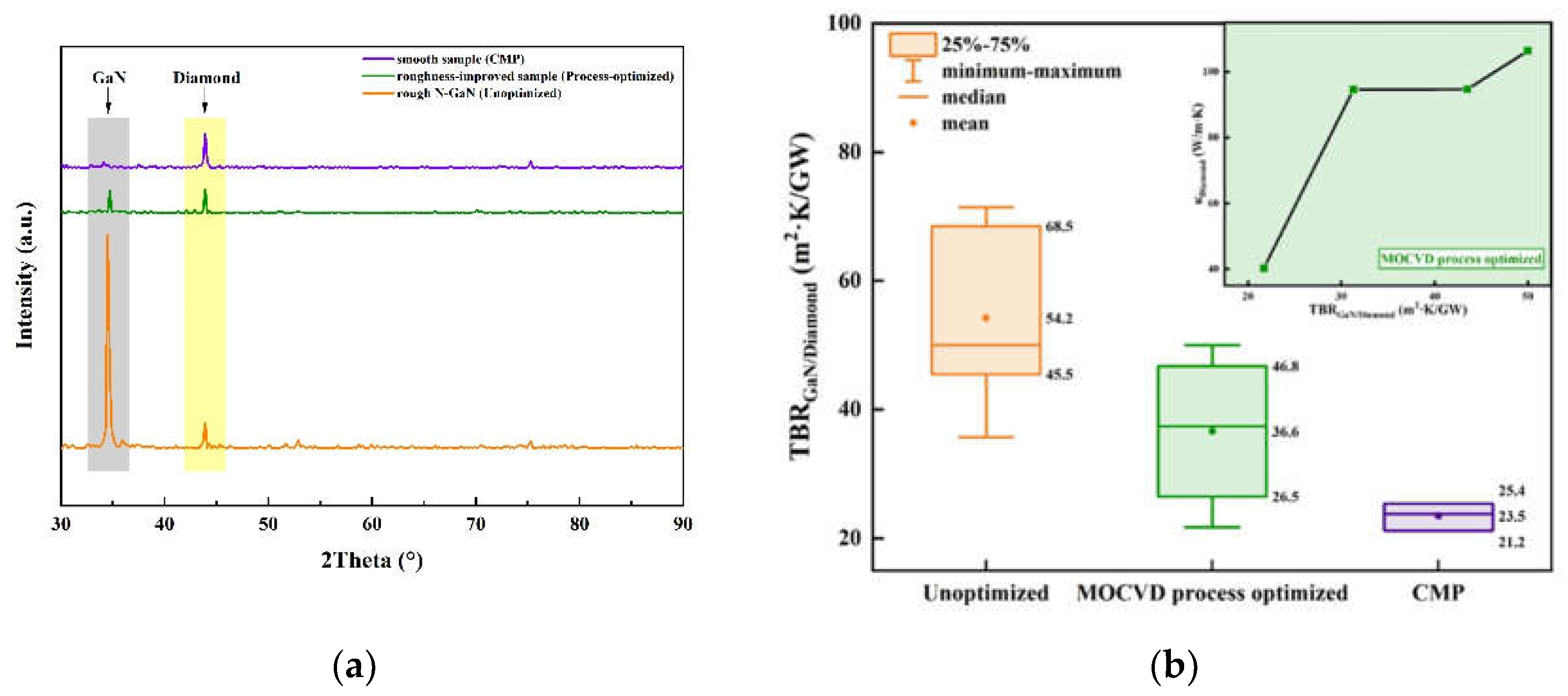
Figure 6a served to further reinforce the impact of surface roughness on seeding and subsequent diamond growth. The pronounced presence of GaN diffraction peaks directly attested to the incomplete lateral growth of diamond films over rough bases. This phenomenon was further exacerbated by the increased base roughness, as evidenced by the intensified GaN peak intensity, which indicated larger exposed GaN areas. An inverse correlation was observed between the intensities of the diamond and GaN X-ray diffraction peaks. In the case of smooth, defect-free NP-GaN layers, the PCD films exhibited complete base coverage, with the GaN diffraction peak virtually extinguished.
The TBR between the diamond and NP-GaN buffer layers was measured and calculated using the TTR technique. In order to comply with the sensitivity constraints of the TTR test, the thickness of the diamond layer was further controlled and reduced to approximately 2.5 μm, thus ensuring the accuracy of the measurement. Figure 6b provided a summary of the TBRGaN/Diamond values obtained on NP-GaN bases with varying surface morphologies. The results indicated that as the surface roughness of the NP-GaN base decreases, the TBRGaN/Diamond generally exhibited a downward trend, with its average value significantly decreasing from 54.2 m2·K/GW to 23.5 m2·K/GW. These findings demonstrated that optimizing the surface roughness of the NP-GaN base could effectively reduce TBRGaN/Diamond to a certain extent. Further analysis demonstrated that samples with elevated base surface roughness demonstrated augmented dispersion in the TBRGaN/diamond values among the tested points. Furthermore, as illustrated in the inset in the top right corner of Figure 6b, test points with elevated TBRGaN/diamond values tended to correlate with regions exhibiting a higher κ of the diamond. These trends were in accordance with the SEM characterization results, which demonstrated that the inhomogeneity of the substrate surface morphology (such as island-like protrusions and stripe clustering) resulted in an uneven distribution of seed crystal seeding density. In regions with a sparse distribution of seed crystals, the NP-GaN base might undergo intensified local etching, resulting in elevated TBRGaN/diamond values and increased variation in the overall TBRGaN/diamond values. Conversely, regions with lower seed crystal density tended to form larger diamond grains during subsequent growth, and these large-grain regions exhibited higher κ due to the reduction in grain boundaries.
4. Conclusions
We reported a new integration strategy of diamond with GaN, with the objective of exploiting the substantial potential of GaN for high-frequency operation in high-power density applications. This strategy involved the direct deposition of diamond films onto NP-GaN epitaxial layers, which circumvented the complexities associated with conventional integration methodologies. By leveraging a high-power condition of 26 kW for PCD growth, coupled with meticulous control over diamond seed seeding techniques and optimization of MPCVD process parameters, a high degree of density in the PCD films has been successfully achieved while preserving the structural integrity of the NP-GaN layer. In order to address the prevalent issue of suboptimal surface quality in NP-GaN epitaxial materials, we studied using CMP technology, which resulted in a significant reduction in surface roughness of NP-GaN to less than 2 nm. This improvement in surface quality provided a smoother wafer surface for subsequent diamond growth. The experimental results indicated that with the improvement of the surface morphology of the NP-GaN buffer layer, the TBR between it and the diamond film decreased progressively. This achievement not only demonstrated the feasibility of using an alternative wafer for the integration of GaN and diamond materials but also offered a potentially efficient solution to the thermal management challenges encountered in high-power electronic devices.
Author Contributions
Conceptualization, Y.W., J.Y. and X.G.; methodology, Y.W.; investigation, Y.W., J.Y.; resources, X.G., Q.F., and X.N.; data curation, Y.W., Y.Y., J.Y. and X.G.; visualization, Y.W.; writing—original draft preparation, Y.W.; writing—review and editing, X.G.; supervision, X.G.; project administration, X.G.; funding acquisition, X.G. All authors have read and agreed to the published version of the manuscript.
Funding
This research was funded by the National Nature Science Foundation of China, grant number 62074033.
Institutional Review Board Statement
Not applicable.
Informed Consent Statement
Informed consent was obtained from all subjects involved in the study.
Data Availability Statement
Data are contained within the article.
Acknowledgments
The authors would like to thank Chao Yuan's group from Wuhan University for providing support of the TTR technique in this work.
Conflicts of Interest
The authors declare no conflict of interest.
References
- Mishra, U.K.; Yi-Feng, W.; Keller, B.P.; Keller, S.; Denbaars, S.P. GaN Microwave Electronics. IEEE Transactions on Microwave Theory and Techniques 1998, 46, 756–761. [Google Scholar] [CrossRef]
- Jones, E.; Costinett, D. Review of Commercial GaN Power Devices and GaN-Based Converter Design Challenges. IEEE Journal of Emerging and Selected Topics in Power Electronics 2016, 4, 1-1. [Google Scholar] [CrossRef]
- Tadjer, M.J.; Anderson, T.J.; Hobart, K.D.; Feygelson, T.I.; Caldwell, J.D.; Eddy, C.R.; Kub, F.J.; Butler, J.E.; Pate, B.; Melngailis, J. Reduced Self-heating in AlGaN/GaN HEMTs Using Nanocrystalline Diamond Heat-spreading Films. IEEE Electron Device Letters 2012, 33, 23–25. [Google Scholar] [CrossRef]
- Zuo, Z.; Tang, N.; Chen, H. Analysis and Improvement of Self-heating Effect Based on GaN HEMT Devices. Materials Research Express 2022, 9, 075903. [Google Scholar] [CrossRef]
- Fujishiro, H.; Mikami, N.; Hatakenaka, M. Monte Carlo Study of Self-Heating Effect in GaN/AlGaN HEMTs on Sapphire, SiC and Si Substrates. physica status solidi (c) 2005, 2, 2696–2699. [Google Scholar] [CrossRef]
- Mendes, J.C.; Liehr, M.; Li, C. Diamond/GaN HEMTs: Where from and Where to? Materials 2022, 15, 415. [Google Scholar] [CrossRef]
- Gu, Y.; Zhang, Y.; Hua, B.; Ni, X.; Fan, Q.; Gu, X. Interface Engineering Enabling Next Generation GaN-on-Diamond Power Devices. Journal of Electronic Materials 2021, 50, 4239–4249. [Google Scholar] [CrossRef]
- Li, C.; Zhang, K.; Qiaoyu, Z.; Yin, X.; Ge, X.; Wang, J.; Wang, Q.; He, C.; Zhao, W.; Chen, Z. High Quality N-polar GaN Films Grown with Varied V/III Ratios by Metal–organic Vapor Phase Epitaxy. RSC Advances 2020, 10, 43187–43192. [Google Scholar] [CrossRef]
- Sun, Q.; Cho, Y.S.; Lee, I.H.; Han, J.; Kong, B.H.; Cho, H.K. Nitrogen-polar GaN Growth Evolution on C-plane Sapphire. Applied Physics Letters 2008, 93, 131912. [Google Scholar] [CrossRef]
- Huo, L.; Lingaparthi, R.; Dharmarasu, N.; Radhakrishnan, K.; Chan, C. Surface Morphology Evolution of N-polar GaN on SiC for HEMT Heterostructures Grown by Plasma-assisted Molecular Beam Epitaxy. Journal of Physics D: Applied Physics 2023, 56, 345302. [Google Scholar] [CrossRef]
- Zauner, A.R.A.; Aret, E.; van Enckevort, W.J.P.; Weyher, J.L.; Porowski, S.; Schermer, J.J. Homo-epitaxial Growth on the N-face of GaN Single Crystals: the Influence of the Misorientation on the Surface Morphology. Journal of Crystal Growth 2002, 240, 14–21. [Google Scholar] [CrossRef]
- Yates, L.; Anderson, J.; Gu, X.; Lee, C.; Bai, T.; Mecklenburg, M.; Aoki, T.; Goorsky, M.S.; Kuball, M.; Piner, E.L.; et al. Low Thermal Boundary Resistance Interfaces for GaN-on-Diamond Devices. ACS Applied Materials & Interfaces 2018, 10, 24302–24309. [Google Scholar] [CrossRef]
- Jia, X.; Wei, J.-j.; Kong, Y.; Li, C.-m.; Liu, J.; Chen, L.; Sun, F.; Wang, X. The Influence of Dielectric Layer on the Thermal Boundary Resistance of GaN-on-diamond Substrate. Surface and Interface Analysis 2019, 51, 783–790. [Google Scholar] [CrossRef]
- Sun, H.; Simon, R.B.; Pomeroy, J.W.; Francis, D.; Faili, F.N.; Twitchen, D.J.; Kuball, M. Reducing GaN-on-diamond Interfacial Thermal Resistance for High Power Transistor Applications. Applied Physics Letters 2015, 106, 111906. [Google Scholar] [CrossRef]
- Keller, S.; Fichtenbaum, N.A.; Wu, F.; Brown, D.; Rosales, A.; DenBaars, S.P.; Speck, J.S.; Mishra, U.K. Influence of the Substrate Misorientation on the Properties of N-polar GaN Films Grown by Metal Organic Chemical Vapor Deposition. Journal of Applied Physics 2007, 102, 083546. [Google Scholar] [CrossRef]
- Malakoutian, M.; Field, D.E.; Hines, N.J.; Pasayat, S.; Graham, S.; Kuball, M.; Chowdhury, S. Record-Low Thermal Boundary Resistance between Diamond and GaN-on-SiC for Enabling Radiofrequency Device Cooling. ACS Applied Materials & Interfaces 2021, 13, 60553–60560. [Google Scholar] [CrossRef]
- Stoffel, A.; Kovács, A.; Kronast, W.; Müller, B. LPCVD against PECVD for Micromechanical Applications. Journal of Micromechanics and Microengineering 1996, 6, 1. [Google Scholar] [CrossRef]
- Malakoutian, M.; Soman, R.; Woo, K.; Chowdhury, S. Development of 300–400 °C Grown Diamond for Semiconductor Devices Thermal Management. MRS Advances 2024, 9, 7–11. [Google Scholar] [CrossRef]
- Meng, B.; Ma, Y.; Wang, X.; Yuan, C. Quantitative Study on Thermoreflectance Linear Relation. Journal of Applied Physics 2023, 134, 115102. [Google Scholar] [CrossRef]
- Goodwin, D.G. Scaling Laws for Diamond Chemical-vapor Deposition. I. Diamond Surface Chemistry. Journal of Applied Physics 1993, 74, 6888–6894. [Google Scholar] [CrossRef]
- Mandal, S. Nucleation of Diamond Films on Heterogeneous Substrates: a Review. RSC Advances 2021, 11, 10159–10182. [Google Scholar] [CrossRef] [PubMed]
- Bolshakov, A.P.; Ralchenko, V.G.; Yurov, V.Y.; Shu, G.; Bushuev, E.V.; Andrew, K.; Ashkinazi, E.E.; Sovyk, D.; Antonova, I.A.; Savin, S.; et al. Enhanced Deposition Rate of Polycrystalline CVD Diamond at High Microwave Power Densities. Diamond and Related Materials 2019, 97, 107466. [Google Scholar] [CrossRef]
- Silva, F.; Hassouni, K.; Bonnin, X.; Gicquel, A. Microwave Engineering of Plasma-assisted CVD Reactors for Diamond Deposition. Journal of Physics: Condensed Matter 2009, 21, 364202. [Google Scholar] [CrossRef]
- Silva, F.; Achard, J.; Brinza, O.; Bonnin, X.; Hassouni, K.; Anthonis, A.; De Corte, K.; Barjon, J. High Quality, Large Surface Area, Homoepitaxial MPACVD Diamond Growth. Diamond and Related Materials 2009, 18, 683–697. [Google Scholar] [CrossRef]
- Andrea, C.L.; Miroslav, K. Theory and Simulation of Crystal Growth. Journal of Physics: Condensed Matter 1997, 9, 299. [Google Scholar] [CrossRef]
- Yoon, M.; Lee, H.; Hong, W.; Christen, H.; Zhang, Z.; Suo, Z. Dynamics of Step Bunching in Heteroepitaxial Growth on Vicinal Substrates. Physical review letters 2007, 99, 055503. [Google Scholar] [CrossRef]
Figure 1.
Integration of GaN and diamond based on NP-GaN epitaxial wafers.
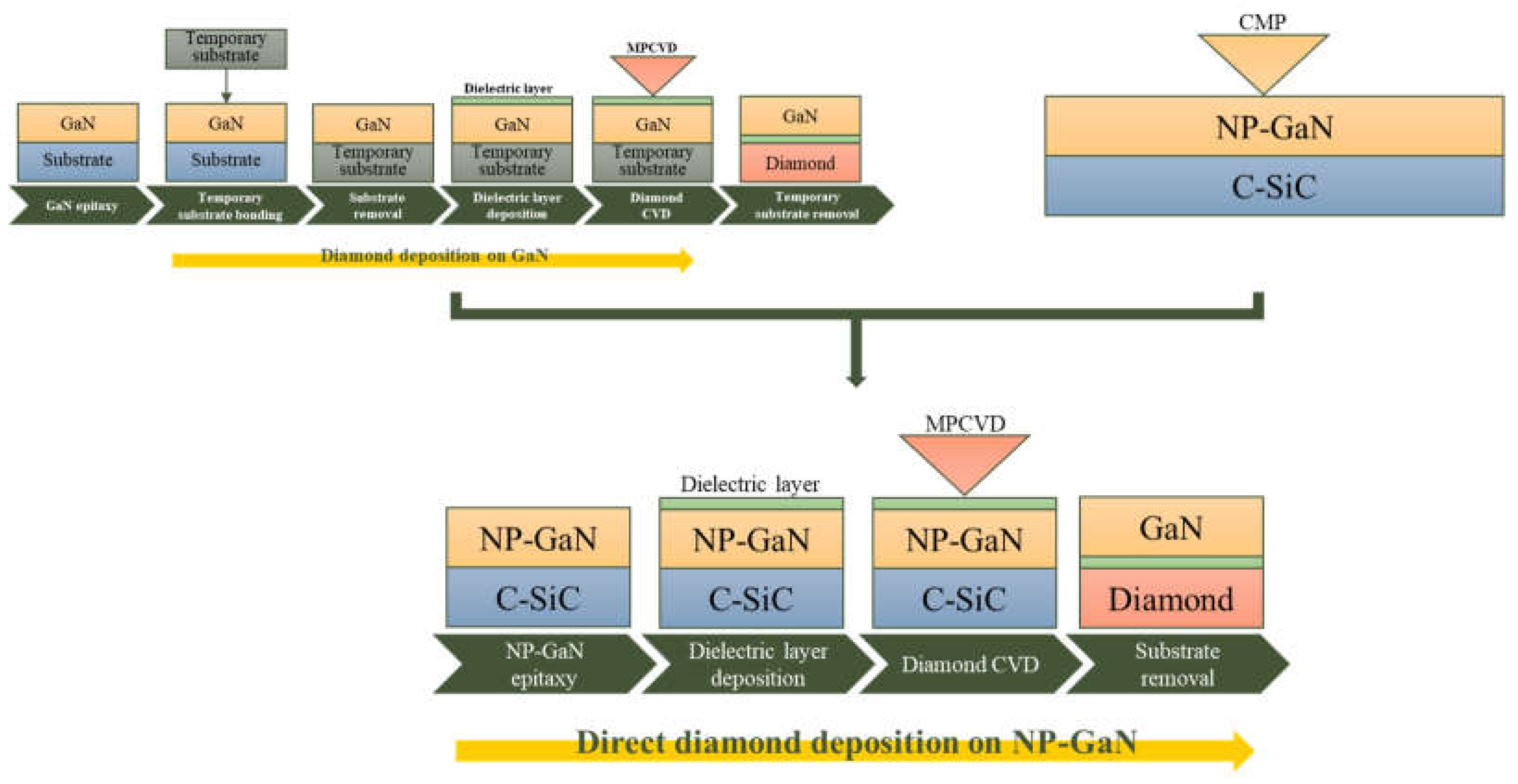
Figure 2.
(a) OM images of seed crystal distributions after spin-coating for seed crystals with a diameter of 5 nm (too small) and SEM cross-sectional images of seed crystals with a diameter of 2 μm (too large) after growth; (b) OM images of seed crystal distributions after spin-coating for seed crystals with a diameter of 100 nm and suspension mass fractions of 0.1%, 0.3% and 0.5%, along with corresponding SEM cross-sectional images of the diamond layers after growth.
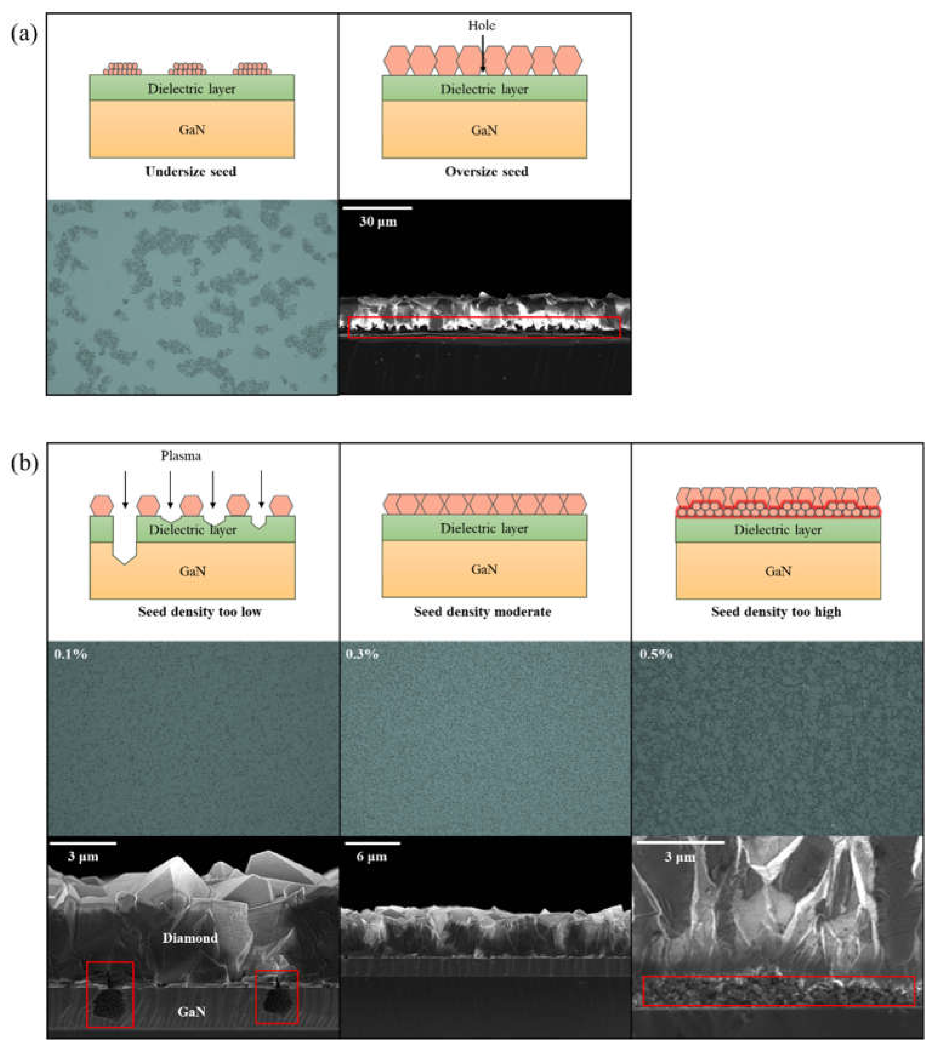
Figure 3.
A cross-sectional SEM analysis of the PCD under the combined effects of the CH4 concentration and plasma power density.
Figure 3.
A cross-sectional SEM analysis of the PCD under the combined effects of the CH4 concentration and plasma power density.
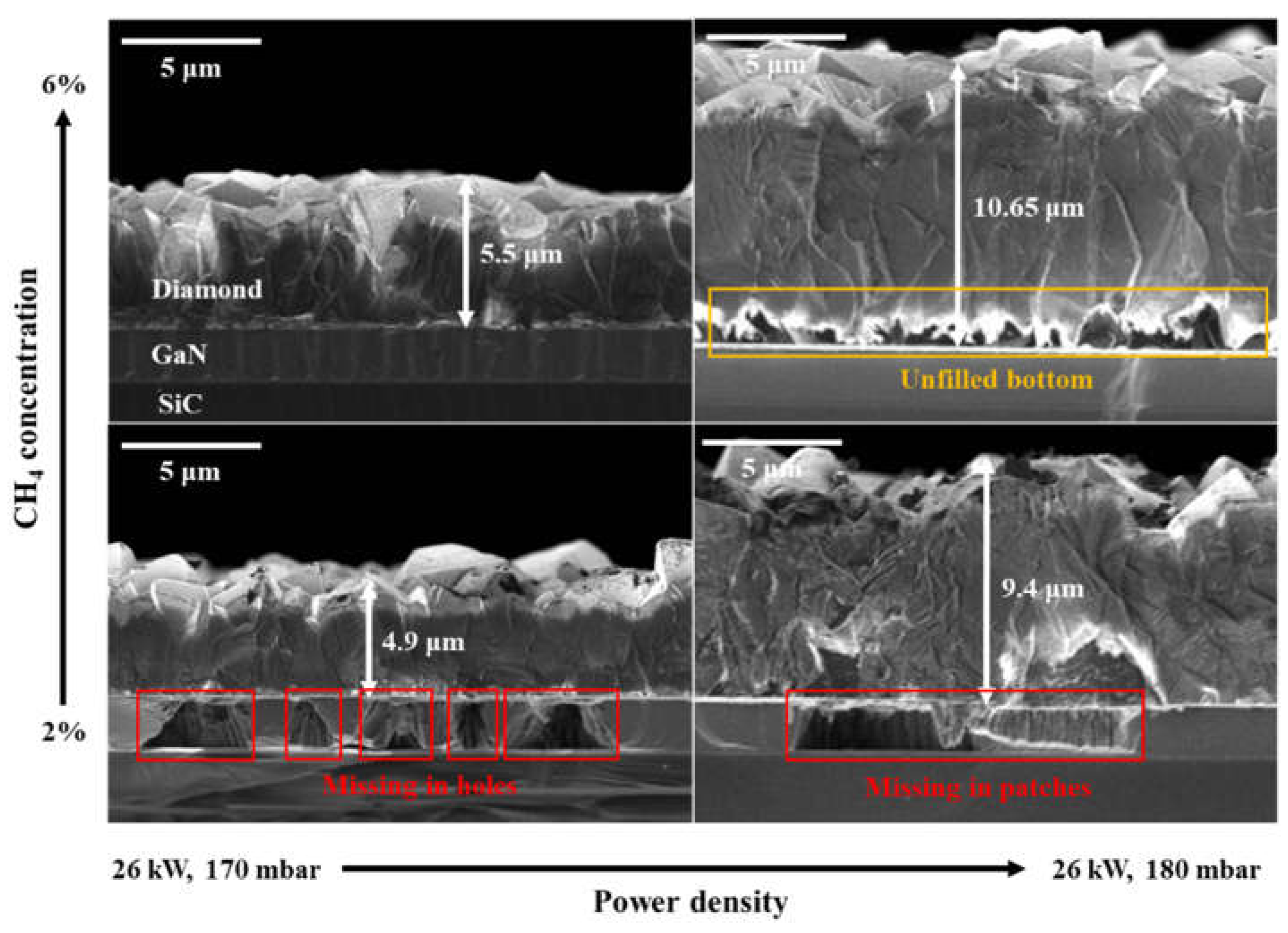
Figure 4.
(a) OM images of the NP-GaN surface morphology without MOCVD process optimization, after MOCVD process optimization and after additional CMP; (b) AFM comparison images of the NP-GaN surface after MOCVD process optimization and subsequent CMP. Insets: Surface morphology height profiles along the direction indicated by the blue line.
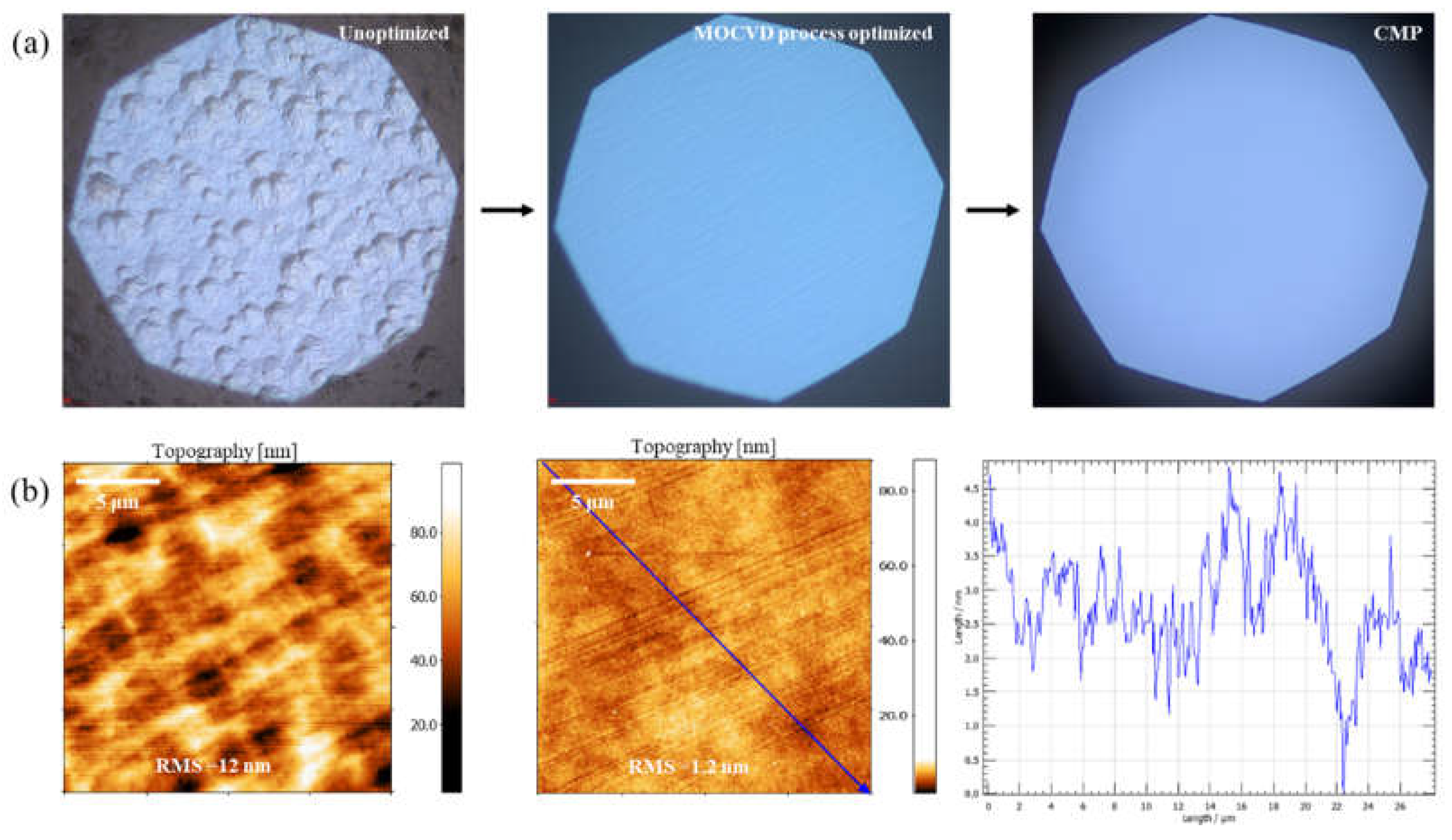
Figure 5.
(a) OM images of diamond seed crystal distribution after spin coating; (b) SEM images of cross-sectional and surface morphology of the grown diamond on NP-GaN bases without MOCVD process optimization, after MOCVD process optimization and after additional CMP.
Figure 5.
(a) OM images of diamond seed crystal distribution after spin coating; (b) SEM images of cross-sectional and surface morphology of the grown diamond on NP-GaN bases without MOCVD process optimization, after MOCVD process optimization and after additional CMP.
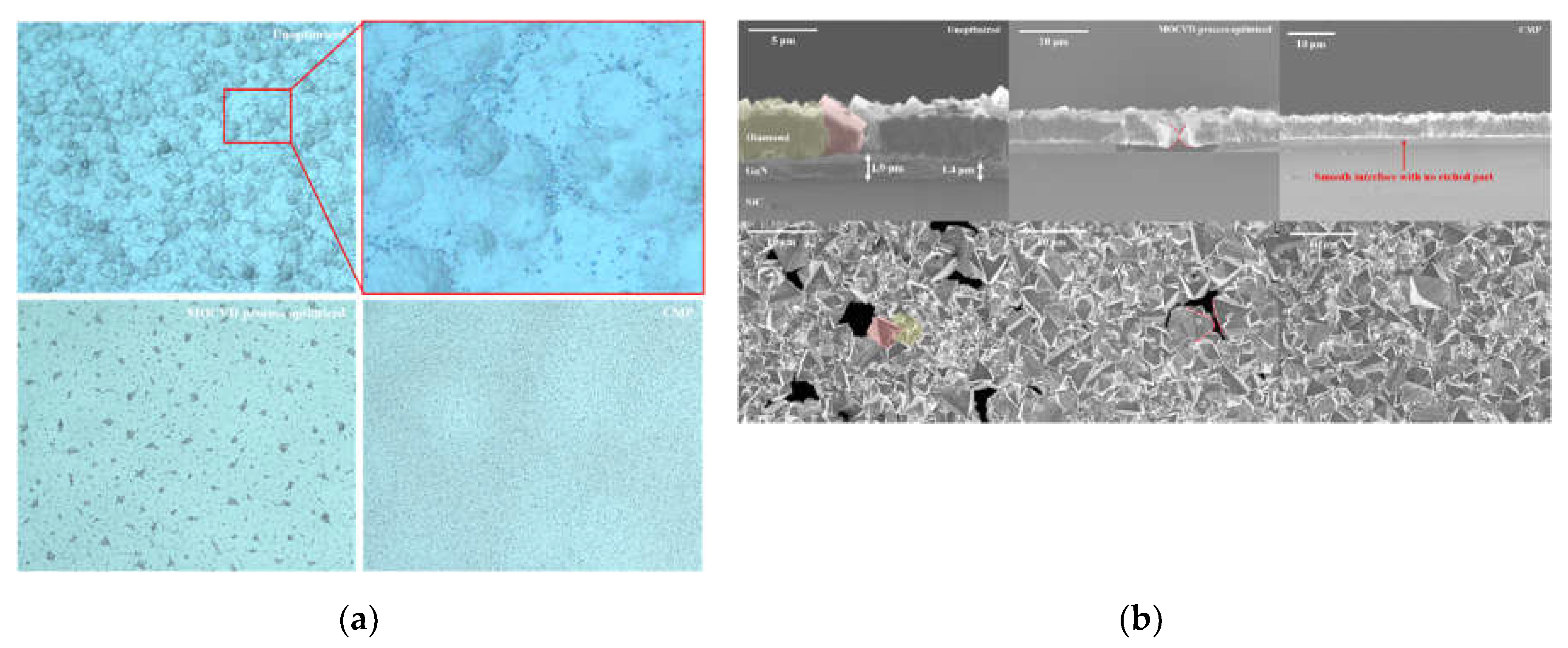
Figure 6.
(a) XRD patterns of the grown diamonds on NP-GaN bases without MOCVD process optimization, after MOCVD process optimization and after additional CMP; (b)TBRGaN/Diamond and its variation across NP-GaN bases with different surface morphologies. The maximum, minimum, median, and mean values are depicted in the box plots. Errors were extracted using a statistic method with the lower/upper limit determined by the 25th/75th percentiles of the corresponding average values of each sample. Inset: A plot of TBRGaN/Diamond versus κDiamond after diamond growth on a NP-GaN base with a relatively smooth surface morphology achieved through optimized MOCVD process parameters.
Disclaimer/Publisher’s Note: The statements, opinions and data contained in all publications are solely those of the individual author(s) and contributor(s) and not of MDPI and/or the editor(s). MDPI and/or the editor(s) disclaim responsibility for any injury to people or property resulting from any ideas, methods, instructions or products referred to in the content. |
© 2024 by the authors. Licensee MDPI, Basel, Switzerland. This article is an open access article distributed under the terms and conditions of the Creative Commons Attribution (CC BY) license (http://creativecommons.org/licenses/by/4.0/).
Copyright: This open access article is published under a Creative Commons CC BY 4.0 license, which permit the free download, distribution, and reuse, provided that the author and preprint are cited in any reuse.


