
Submitted:
27 March 2025
Posted:
28 March 2025
You are already at the latest version
Abstract
Single UIS and repetitive UIS experiment are performed in this article to expound physical failure mechanisms in P-GaN Hemt devices. Vpeak versus Ipeak as the metric to evaluate the degradation of electrical parameters. In single UIS test, different load inductors, off-gate voltage and ambient temperature are chosen as variables to observe the failure phenomena in device under test(DUT), while in repeated UIS tests, threshold voltage, on-state resistant, blocking characteristics and gate leakage current degradation and recovery are concluded and analyzed that Vth presents a negatively shifting, Ron and BV will restore to their initial value, gate leakage shows a significant reduction at first and then after a duration of lagging will gradually recover to some extent but unable to achieve to its initial value. Combing failure point analysis by decaping with TCAD simulation validation, hole trapping and detrapped dominate Vth and Igss degradation, while Ron and BV degradation are dominated by electron traps in buffer.
Keywords:
P-GaN HEMT
; UIS
; failure analysis
; degradation and recovery
1. Introduction
Due to their excellent electronic properties, such as high electron saturation velocity and high breakdown voltage, GaN-based high-electron mobility transistors (HEMTs) have confirmed them to be leading transistor technology for future high-power devices at high-frequency operation. However, one of the critical disadvantages of GaN power devices is the lack of unclamped inductive switching (UIS) capabilities [1,2]. It is well-acknowledged that due to the existence of inductive loads and parasitic components in circuits, power devices may also suffer from UIS strikes, which occurs during the switch-off process. Theoretically, if the inductors are unclamped, the current stored in the inductors will surge through the power device from drain to source at the switch-off transient, and then, the voltage dropped on the device is enlarged rapidly. In this way, the device suffers from high-current and high-voltage stresses at the same time, which may lead to severe parameter degradations.
As known, because of the lack of avalanche process in GaN HEMT devices, they possess weaker UIS capability compared to Si-/SiC-based counterparts. For Si-/SiC-based devices, avalanche energy (i.e., the surge energy during the UIS process) is the decisive factor in damaging the devices. The avalanche is an impact ionization (I.I.) and multiplication process that usually occurs at the p-n junction. There are two different views about UIS failure in P-type GaN HEMT. One is related to avalanche multiplication, and the other is non-avalanche, that is, LC resonant. Device failure is only related to the high electric field under high voltage [3].
Bao et al. [4] and Sheng Li et al. [5] think that avalanche breakdown could be found in P-type GaN HEMT devices to a certain extent, while the UIS avalanche energy it can withstand is relatively small, only at the µJ level. The holes generated by impact ionization will be accumulated and give rise to avalanche multiplication and current increasing, leading to thermal runaway. Naka and Saito reported that the UIS withstanding capability of p-GaN HEMT can be designed from the viewpoint of hole removal, which is related to the gate leakage current. Marek et al. analyzed the influences of different load inductances and different supply voltages on the UIS withstanding capability of p-GaN HEMT. Reference [6] presented the results of repetitive UIS stresses on normally ON HEMT; moreover, a deep-level transient spectra (DLTS) analysis was taken to study the degradations of OFF-state leakage current to determine whether holes or electrons are the dominant factor of device failure. Many researchers think that avalanche phenomena and the charge captured by defects exert a profound influence on GaN devices, and capture mechanisms of defects in the interface of heterojunction and barrier are attributed to the cause of electrical performance under UIS stress [7,8,9]. In 2022, Zhang et al. [10] clarified the surge-energy withstand mechanisms and failure physics of commercial GaN GITs. They summarized their main differences compared to the ones of Si and SiC MOSFETs. Their results suggested the avalanche energy, a widely used JEDEC standard for the robustness of Si and SiC power MOSFETs which represents the device capability to resistively dissipate energy without thermal runaway, may not be a proper parameter that can directly represent the surge energy robustness of GaN HEMTs. Avalanche robustness in GaN HD-GIT depends on overvoltage pulse created by UIS test and additional FIB analysis shows failure point was near to the drain region. Simultaneously, they thought that the variation of Vpeak versus Ipeak can preferably evaluate the UIS capability of GaN devices.
For clarifying the electrical failure behavior of P-GaN HEMT under UIS stresses , single and repetitive UIS stresses measurement has been performed with Vpeak and Ipeak chosen as the criterion of parameters degradation. In this article commercial products from GaN System Inc. (GS66508T), which can withstand above 650-V high voltage and conduct above 30-A high current, are adopted as the studied target devices. The influence of different load inductors, Vgs_off and ambient temperature on the characteristics of DUT under single UIS pulse is measured and evaluated. Meanwhile, in repetitive UIS stresses, threshold voltage, on-state resistance, blocking characteristics and gate leakage degradations and recovery mechanisms are elucidated. Finally, combination of decapsulation and failure location analysis and TCAD simulation is used to explore systematically and comprehensively the failure mechanisms of DUT under UIS stresses.
2. Device Structure and Experimental Setup
Figure 1 gives the cross-section of P-GaN Hemt in our work. The measurements were taken using DUTs listed as GaN Systems GS66508T as shown in Figure 1a as an enhancement mode Schottky P-Gate GaN-on-silicon HEMT rated at 1.1~2.6 V, 30 A, 650 V, and 50 mΩ with an area of 6.9 mm × 4.5 mm encapsulated in surface mount packages with top-side cooled. Figure 1b is the illustrative drawing of DUT in our work.
Figure 2a shows schematic of typical UIS test schematic and Figure 2b shows typical gate pulse VGS applied to gate electrode of DUT , Figure 2c,d shows VDS and IDS waveforms under UIS stress of Si/SiC MOS(c) and GaN HEMT(d) respectively. Figure 2e presents the back of test board. VDD, inductive load, DUT, gate driver and PWM input are marked with yellow frame. Different from Si/SiC devices with a dynamic UIS avalanche processing, it is well known that because there is no traditional pn junction connecting source and drain of GaN Hemts, which posses current transport theory due to heterojunction and 2D electron gas channel existence, leading to a minimal avalanche capability and even no avalanche capability. Comparing UIS waveforms of GaN HEMTs with the ones of Si/SiC mosfets in Figure 2c,d, when VGS switches off, the energy stored in the load inductor flows through DUT, meanwhile, because of lacking of avalanche process, the VDS applied to the GaN HEMT increases gradually to maximum value while comparatively the voltage dropped between drain and source of Si/SiC mosfet is clamped to a constant value. As the displacement current appears, the VDS dropped on GaN HEMT goes down. The entire UIS period seems a LC resonant. Notably, when loop current IDS in Figure 2d drops to zero, simultaneously, VDS achieve to peak value. And after that IDS decreases further to a negative value. Current value at t4 equals to absolutely the one at t2 and this phenomena indicates that the energy stored in load inductor dissipated didn’t rely on avalanche, insteadly, rely on the LC resonant of load inductor and parasitic capacitance in the body and thus may lead to severer parameter degradations and even catastrophic failure [11].
Actually, due to measurements error and other uncontrollable factors, the zero point of current in Figure 2d is usually not coincident with the time point of maximum value of voltage, that is, t3 will shift a little. During t3~t4 period, energy stored in output capacitance Coss of DUT will dissipate through load inductor, since existence of Ron and charge imbalance caused by trapping and detrapping of dynamic Ron [12] of DUT , energy consumption Eloss would occur but only at uJ level. Surge energy could not be dissipated through avalanche as the one of Si/SiC counterparts and could be insteadly consumed by LC resonant consisted by load inductor and Coss [13]. When t4 is reached, VDS generated by LC resonant can arrive to a negative value and exceeds its reverse threshold voltage, thus, DUT is in 3rd working operation [14]. At this moment, the circuit will dissipated the energy by power supply of Vdd loop [15,16].
3. Parameter Degradation and UIS Ruggedness Analysis
3.1. Single UIS Test
Figure 3 shows the typical room temperature single UIS waveforms of p-gate GaN Hemt during the last test before failure (Figure 3a) and at failure (Figure 3b) under 0.3 mH of inductive load conditions, respectively. Test conditions is as: power supply is 30V and gate driver voltage is switched from -4V to 6V. From Figure 3a, when gate pulse width of 12.15μs is applied on gate-source of DUT, the peak current value of drain-source is 620mA, while the VGS switches from 6V to -4V, the induced voltage is applied between drain and source with peak value about 1.324kV at this moment the current equals to zero. During the entire UIS process, VDS rises from 0 to VDS,max and then drops to 0, IDS linearly decrease to a negative value and then increase to 0. The entire process lasts about 0.85μs and is similar to LC resonant [17]. During the reverse of IDS period, after a duration of reverse conduction, VDS starts to oscillate and then damps to 30V. In Figure 3b, when gate pulse width increases to 12.20μs, the charging period of inductor increases either and the peak value of IDS will achieve to 630mA. Then after the DUT is switched off, VDS increases rapidly to the highest point of voltage of 1.332kV at which DUT failed. After DUT failed, VGS keeps constant at -4V and VDS approaches to zero [18]. After then, the current rapidly increases, which shows that the short circuit of source and drain happens after DUT failed. At this moment, DUT behaves like a passive low impendence.
By varying different test conditions such as load inductance, Vgs_off and temperature, a series of single pulse UIS tests are conducted by gradually increasing the gate pulse to obtain failure point, and then, peak currents and peak voltages under different working conditions before device failure are extracted and concluded in Figure 4. Datas in Figure 4a are obtained under different inductance, (b) at different Vgs_off;(c) at different temperature.
It can be found that in Figure 4a, with inductance increasing the peak current will obviously decreases because of increasement of charging and discharging period of load inductance , and the UIS process period will also increase. Meanwhile, critical VDS shows little floating before device failed and less significant relationship with load inductance [19]. In Figure 4b, we can see that both peak current and critical peak voltage between drain and source show a little floating which maybe caused by devices differences, and have no obvious changes with variation of Vgs_off. Figure 4c presents critical voltage versus peak current before failure under different ambient temperature, and shows no obvious relationship with temperature and likely some fluctuations.
In order to verify the failure mode under single UIS test. The failed sample with different failure mode is decaped and delayer, after local corrosion treatment without damage, optical microscope(OM) is used to observe and validate the failure point by adjusting magnification [20]. Figure 5 shows the OM imagines of decapped failure samples and waveforms at failure. Figure 5a and 5c show the decap results of the failed devices. Figure 5b,d are measured UIS waveforms when (a) and (b) failure occurs respectively. The failure test conditions is under 75°C with VGS switches from -4V to 6V, load inductance L equals to 3mH in Figure 5a,b, VDD is 30V and 25°C, -4V~6V, 3mH and 30V in Figure 5c,d, respectively. we can see from Figure 5a that slightly burnout compared with Figure 5b happens in the drain metal strips region and gate region, we can confirm that the failure is caused by breakdown of drain and gate damage. Since burnout area is very small and no sharply increasement of IDS occurs in captured curves in Figure 5b so that we can confirm that no short circuit occur between drain and source [21]. Comparatively, as presented in Figure 5c that large burnout arear is found near the drain and obviously damaged arear in the surface and around gate region. So, the main failure reason of chip is related to short circuit of drain and source caused by drain failure and finally burnout with IDS increasing sharply as shown in Figure 5d. Meanwhile, gate electrode is also subjected to great UIS stress and leading to damage which is consistent with the captured waveform in Figure 5d.
3.2. TCAD Simulation Under Single UIS Stress
To further explore the UIS failure mechanisms, TCAD simulation is synchronously used to explain the failure behave. In the simulation, the structure of the p-GaN gate HEMT comprised a 2.0 μm-thick GaN layer, a 15 nm AlGaN barrier. layer with 23% Al, and a 100 nm p-GaN layer. The gate length was 1.5 μm, the source-gate distance was 1 μm, and the gate-drain spacing was 17 μm. The doping concentration of the p-GaN layer was 3 × 10⁻¹⁷ cm−3. Besides above, to coincide well with the experimental datas, some corrections should be done in the key structure region. Firstly, interface states are intentionally added to AlGaN/GaN interface to explain the net polarized charges due to the piezoelectric polarization effect generated in AlGaN/GaN structure. Besides, since body traps play an important role during the UIS processing, acceptor traps in the GaN channel should be introduced with concentration of and energy level higher above valence band about 0.9eV. Trap concentration in buffer should be higher much than the ones in channel region and the concentration is calibrated as with energy level as same as the one in channel traps. Besides above deep-level traps, owing to the existence of heterojunction interface and processing treatment, various traps could be introduced. Shallow level traps in the interface should be taken into consideration either. In our simulation, the interface states concentration is set as within the range of and energy level is 0.05~0.8 eV above valence band. After the well calibration of device structure, UIS processing is performed by the method of Mixed-Mode. The circuit parameters are set as follows: the load inductor L is set as 3mH, driving voltage VGS is about -4~6V, supplied bus voltage VDD is set as 30V,conduction duration ton is set as 70μs, simulated waveforms is shown in Figure 6b, the peak voltage and peak current is respectively almost 1.3 kV and 400mA which are close to experimental dates.
Electrical field and impact ionization versus X-coordinate are extracted at Vpeak point and plotted in Figure 7a. Total current density, electron density and hole density profile are extracted and plotted in Figure 7b–d. Seeing from Figure 7a that when DUT suffered from UIS stresses, a huge voltage is dropped between source and drain, meanwhile, a large electrical field and strong impact ionization focused around drain region and then at the edge of gate field plate and source field plate. we can see from Figure 7b that there exist three current conduction paths: current from drain flows through channel and arrive to source, the other one is current from drain passes through buffer and reach to source, the third one is current passes through buffer and flow to gate [22]. Combination of Figure 7a,b, it can be concluded that when the DUT suffered UIS stress striks, a large voltage is generated between drain and source and impact ionization will occur under drain electrode and thereby massive electron-hole pairs could be generated. Electrons generated would be trapped by buffer while one part of holes generated would move along channel and pass through buffer and then move to substrate, another part of holes would move to gate due to the electrical field of drain to source and then one part flow into P-GaN layer and the other part accumulated benethe the gate and finally resulting in three current conduction paths. Concluded from these four figures that DUT failure is mainly caused by huge electrical field dropped on drain which exceeds the dielectric limitation and thus leading to dielectric breakdown and DUT has been damaged. Which is different from SiC power MOSFET [23,24].
3.3. Repetitive UIS Stress
Figure 8 illustrate the repetitive UIS waveforms diagrams. Repeated UIS stresses measurement at room temperature is performed in this session and the test conditions are follows: load inductor equals to 3mH, power supply is set to 30V, gate bias switches from -4V to 6V, conduction duration is 16 us. Under such electrical conditions, each time when UIS stress strikes, Vpeak between drain and source arrive to 1.1kV which is 80 percent of critical voltage with Ipeak equaling to 360mA. Additionally, for heat dissipating effectively before next stress striking, duty ratio of gate pulse is set to 0.1% with frequency 62.5Hz, that is, interval between each pulse is 16ms, besides, fan is laid aside closely and used to cool surface temperature down.
3.3.1. Degradation of Vth
After a certain amount of UIS stress cycles, the following typical static and dynamic electrical performances are measured: transfer characteristic(Vth), output characteristic(Ron), breakdown voltage(BV) ,gate to source leakage current with short drain to source (Igss),and plotted in Figure 9, Figure 10, Figure 11 and Figure 12, respectively.
Figure 9 presents measured Ids versus Vgs waveforms of DUT under repetitive UIS stress. The transfer characteristics are obtained from measuring instantly after stress in Figure 9a, with 30min delay in Figure 9b, with 24h delay in Figure 9c, respectively. Variation of Vth with cycles extracted at Ids=100 mA is presented in Figure 9d. Test conditions are as: VDD=30V, Freq=62.5Hz, Duty ratio=0.1%,Vds=1V.
Figure 9a shows an obviously positive shifting after 1k、10k、100k、200k repetitive UIS duty cycles when measuring Ids versus Vgs instantly after stresses. That is, threshold voltage will increase, however, there is no reasonable mathematic relationship between shifting level and duty cycles, such as a simple linear proportional with UIS cycles. After the other 30mins lagging, Ids vs. Vgs were extracted and plotted in Figure 9b we found that the Vth will negative shifts and also shifting level has no a visible mathematic relationship with UIS cycles. Combining Figure 9a,b we can conclude that Vth will positively shifting at first and then reversely shifting after a certain UIS cycles which rule is close to that given in [3]. And then continuously after 24hs lagging and extract Ids vs. Vgs to present in Figure 9c that Vth of DUT continues to exhibit negatively shifts compared with not undergoing UIS stresses, but the shifting degree to some extent reduced compared with the one measured after 30mins lagging.
In Figure 9d, we can see that after repeated UIS cycles, under different lagging duration, there is no direct linearly relationship between Vth degradation with cycles. Meanwhile, at a fixed cycles, Vth shows an obvious reduction. While with increment of UIS cycles the decrement degree of Vth will finally keep a constant tendency and has a certain of reduction compared with the initial value except for the circumstances when measuring Vth instantly after stresses.
3.3.2. Ron Shifts
Figure 10a presents Ids versus Vds measured instantly after UIS cycles. An obvious increment of Ron is found and no visible mathematical relationship with repetitive UIS cycles. DUT undergoing 1k UIS cycles has achieved maximum Ron increment and then the one subjected to 100k UIS cycles. Ids versus Vds is measured again after additional 30mins lagging and are plotted in Figure 10b. From the graph, it is considered that Ron of DUT increases slightly compared with the one undergoing no UIS cycles which shows that Ron recovered a certain. Further output characteristics measurements are performed continuously after 24hs lagging and plotted in Figure 10c. As shown in Figure 10c that after a long period, Ron of DUT almost recovered its initial state while a small increment could be found when DUT undergoing 200k UIS cycles.
Variation of Ron versus UIS cycles is calculated from output characteristics and plotted in Figure 10d.The working conditions are as follows: VDD=30V, Freq=62.5Hz, Duty ratio=0.1%, Vdd=30V with Vgs=6V, repetitive UIS stress is set as: zero cycle, 1k cycles, 10k cycles, 100k cycles, and 200k cycles. We found after computation that the initial value without UIS cycles is 47.5 mΩ, after 1k cycles stress and measuring instantly Ron has the maximum increment of 5 mΩ about 10.5% increment and achieves to 52.5 mΩ. Then after the other 30mins lagging, Ron is reduced to 49.25 mΩ with a reduction of -3.25 mΩ and -6.2% amplitude reduction. It seems that after repeated UIS cycles, Ron finally restored to its initial value although there exists increment and decrement alternately during entire UIS cycles.
3.3.3. BV Shifts
Figure 11 presents blocking characteristics under repetitive UIS cycles, test conditions is illustrated and inserted in figures. Figure 11a is measured instantly after UIS cycles, could be found in Figure 11a that breakdown point right shifts and shifting degree does not proportional to UIS cycles. Among these five curves , the one suffered 10k UIS cycles has the maximum rightward. After the other 30mins lagging and measuring the blocking characteristics and plotting them again in Figure 11b. Seeing from Figure 11b that all of breakdown point measured from DUT move left. And the DUT suffered 200k cycles left shifts mostly, while the DUT undergoing 10k cycles has a certain recovery but compared with initial state it shows slightly increasing. After DUT is kept on 24hs continuously and measures its blocking characteristics, then plotting it in Figure 11c that almost most curves recovered and only the curve suffered 200k cycles shows left shifts.
BV is extract from Ids versus Vds at Ids=50 uA with gate is biased at zero and plotted in Figure 11d. UIS cycles stress set is as before. The initial BV without UIS cycle is 1068V. At 10k UIS cycles, most of BV has presented right shifting and achieve to 1078V about 0.93 percent increments. After the other 30mins lagging, BV has restored to the initial value at 1k UIS cycles, when UIS cycles has increased to 200k, BV has reduced to a smaller value than initial value and pre-breakdown has happened. While after keeping on 24hs lagging, BVs of DUT suffered 1k, 10k and 100k cycles almost keep constant with initial value, while BV measured exceeding 200k UIS cycles has reduced to 1058V of 0.93 percent decrement. Above all, seeing from Figure11d we can found that with increment of UIS cycles, if the lagging is the same, the BV increase at first and then dropped to the initial value , when UIS cycles applied exceeds a certain amount ,BV will decrease gradually and eventually will not return to its original state.
3.3.4. Gate Leakage Degradation
Figure 12 shows gate leakage Igss with drain short to source and gate voltage sweeps from 0 to 5V gradually. Figure 12a shows the curves measured after instantly UIS cycles. It is obviously found that gate leakage Igss decrease significantly and presents almost proportional to UIS cycles, that is, the more UIS cycles, the more Igss decreases. Figure 12b shows the Igss after the other 30mins lagging and can be found that gate leakage Igss increase slightly compared with the ones in Figure 12a, Igss increases from 1.89uA to 2.33uA after suffered from 200k cycles strikes. And DUT suffered from 1k cycles almost recovered to its initial value and the red curve almost overlaps with the black one. After another 24hs lagging, Igss is measured and then plotted in Figure 12c, we can found that DUT suffered from 1k and 10k cycles strikes will not recovered ,while the DUT suffered from 200k recoveres to its state with 100k and reflected that the purple curve overlaps with the green one.
Figure 12d concludes Igss versus UIS cycles. All Igss extracted from Figure 12a–c with zero UIS cycles, 1k cycles, 10k cycles, 100k cycles and 200k cycles under Vg=5 V. Obviouly, it can be found that Igss decreases at first and is linear to UIS cycles, and then reduces to a constant value. The initial Igss is 10.22 uA without any UIS cycle stress, after 200k cycles strikes and then measures instantly, Igss reduced to 8.33uA with amplitude decrement reaches to 81.5%. In Figure 12d, the red curve almost overlaps with the blue curve which means that after a long time lagging, DUT remains in a stable state but will not return to its initial state and keeps a distance with the black curve. Therefore, DUT with 24hs lagging keeps stably and Igss reduces to 2.46 uA with 75.9 percent reduction compared with 7.76 uA measured instantly after cycles. Conclusively, Igss can return to its initial level within a range of UIS cycles but if the cycles exceed special value, Igss recovers a little and shows a significant reduction compared with zero UIS cycles.
3.4. Degradation Mechanisms Under Repetitively UIS Stresses
Figure 13 gives the equivalent circuit model of gate region in P-GaN HEMT. Gate region is formed by combination of back to back Schottky diode and p-i-n diode, Schottky diode is formed by gate to metal and p-i-n diode is formed by P-GaN/i-AlGaN/N-GaN. Due to the band gap discontinuity in the interface and defects induced by processing, traps can not be ignored [25,26,27].
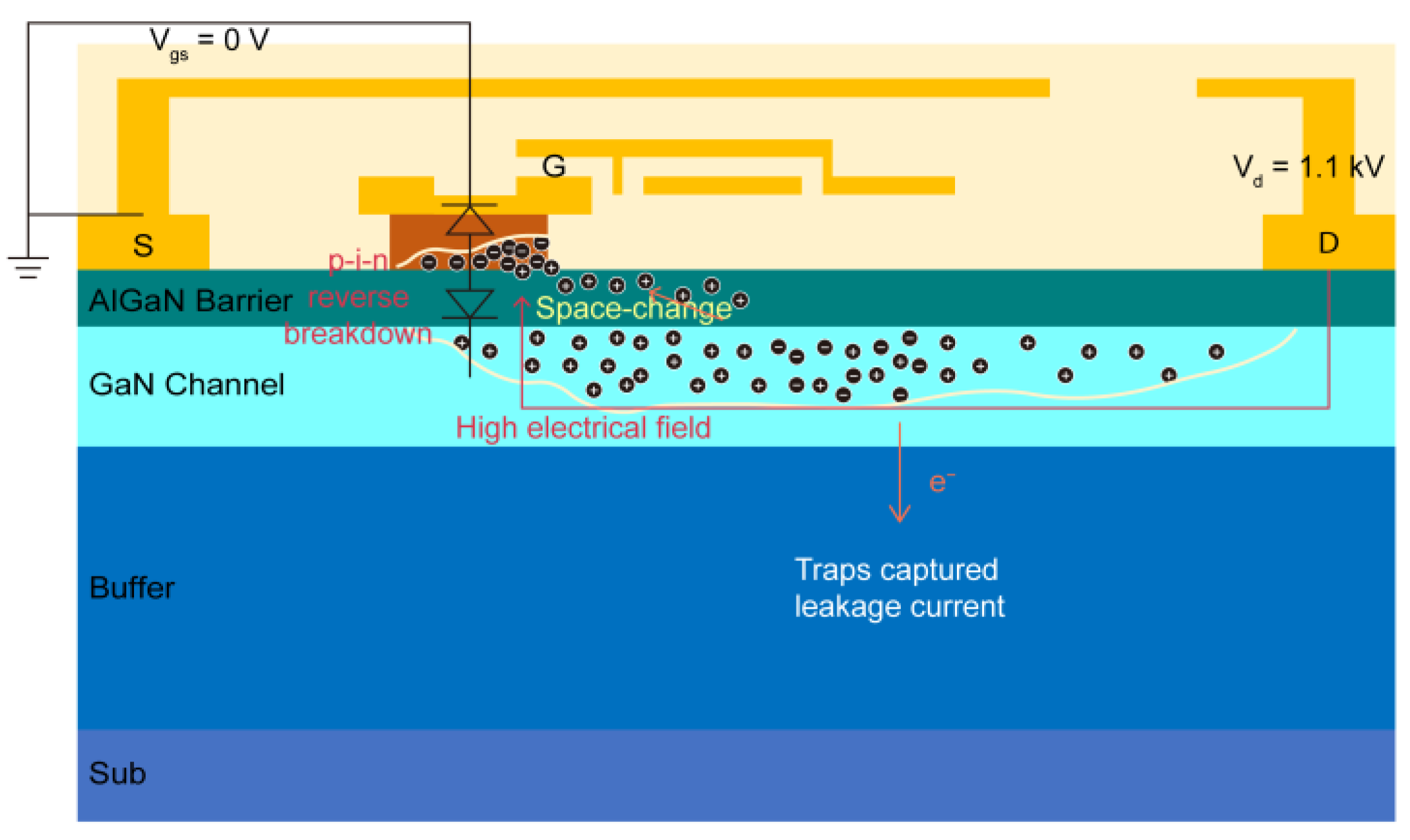
Figure 14 illustrate the impact ionization process and electrical field profile when UIS stress is applied to the DUT. Because UIS often occurs at the moment of Vgs switches from Vgs_on to zero, thus, VDD is set as 1.1kV, and gate is shorted to source as shown in Figure 14.When DUT is striked by UIS stress, a large induced voltage is applied between drain and source. Strong impact ionization will occur in the body leading to a huge amount of electron-hole pairs generated. A high electrical field will be induced between drain and gate marked with red line , meanwhile, a vertical electrical field directing from N-GaN to P-Gan is generated near gate electrode, and then drives p-i-n diode entering into reverse blocking state. P-GaN acts as negative charge center of space-charge region, N-GaN acts as positive charge center of space-charge region. Holes generated by impact ionization were injected into gate and barrier, then captured by trap nearby, while the electrons were captured by traps in buffer.
When single UIS is performed as known as before, duration of stress only lasts for several micro-seconds and since electron mobility is much larger than hole mobility, Besides, in range of a short time after the UIS stress is removed, channel electrons were trapped into electron traps in GaN buffer, amount of holes accumulated beneath gate. Besides, when UIS stress is removed, both of Schottky diode and p-i-n diode is in off state, there is no extra holes entering into P-GaN region and recombination with negatively space charge, and a negative charge center is left instead. At this moment, to turn on the DUT a pre-positive voltage should be necessary and applied to gate electrode to offset the electrical field brought by negative space-charge. Thus, threshold voltage consists two parts: one is the pre-positive gate voltage(△V) and the other is the gate voltage required to channel forming(Vth0), that is, Vth0+△V reflected in Figure 9a that Vth slightly increased when measured instantly after UIS stressing.
Under the condition of high-voltage bias appeared between gate and drain during UIS stresses, electrons get trapped at interface between gate and drain which performs as “virtual gate” and “virtual gate” will extend the depletion region beneath the gate to the source and drain, and additionally exhaust the channel electrons, leading to increasing of Ron. Since the virtual gate can not restored rapidly to its initial state after UIS stresses are removed, Ron when measured instantly after UIS stresses will show increasing tendency. This phenomena is consistent with those presented in Figure 10a. Besides the effects of virtual gate, electron-trap in N-GaN buffer also play the role that Ids will decrease either which is reflected in Figure 11a that BV presents a increasing tendency.
As previously described, under the conditions of high gate bias voltage, for p-i-n diode, a negative charge space is formed in P-GaN region, and a positive charge space is formed in N-GaN region. In a short time after UIS stresses is removed, due to both diodes are in off-state, there are no extra holes provided to recombine with negative space charge and electron traps in the buffer region can not also immediately release all the trapped electrons to recombine with positive space charge in N-GaN region. Thus, existence of space charge will greatly reduce Igss which phenomena also consistent with Figure 12a.
After a period of UIS stresses removed, holes underneath the gate electrode will recombine with the negative space charges in P-GaN region, thereby, holes will accumulate in P-GaN region and Vth will decrease and shows negatively shifts. Meanwhile, electron traps in barrier and passivation layer will release the trapped electrons, virtual gate vanishes, on-state resistant gradually restores to its initial value. Electrons released by trapps in buffer will flow into channel which results in the amounts of electron is larger than that of holes and Ids will increase presented as BV left shifts. Because the space charge width resolved itself to some extent, gate leakage has a certain restored also. Above analysis is consistent with the curves with 30min lagging in Figure 9b, 10b 11b and 12b. That is, Vth shows negatively shifting, Ron returns nearly to its initial value, while BV little decreases and gate leakage with drain short to source restores a certain extent.
Under repeated UIS stresses, inside the DUT, continuous impact ionization produce electron-hole pairs, electrons trapped and detrapped, recombination of electron-holes, space charge region widen and recovered. During these processes, due to hole mobility is much less than that of electrons and there are barriers above and below P-GaN layer, it is hard for holes injected into P-GaN to return to its initial position, accumulated holes in P-GaN region in last stress hasn’t been consumed not yet, the next stress strikes again. Thus, after repeated UIS stresses, gate will be damaged permanently and it is hard for threshold voltage and gate leakage current to return to its initial level. However, formation and disappearance of virtual gate, channel current is dominated by electron-traps, after a long time of lagging, channel resistant and blocking characteristics can almost return to their initial level. While for DUT undergoing much more repeated UIS stresses such as 200k striks, the buffer layer suffered much more and the blocking characteristics has irreversible degradation.
4. Conclusions
Electrical parameters degradations of p-GaN HEMTs under UIS stresses have been investigated in this article. Single pulse and repetitive UIS test under different working conditions are performed to evaluate parameters degradations and recovering. With the help of TCAD simulation and damage position analysis we can conclude that the failure mechanism under UIS stress is dominated by dielectric breakdown caused by high electrical field around drain electrode and gate damage. While, after UIS stress strikes, Vth at first positively shifted and then negatively shifts and at last be stable at a negatively shifting value, Ron and BV increase at first and gradually returned to its initial value. While after repetitively UIS striking with different lagging period, gate leakage current reduced significantly firstly and gradually recovered, but can not completely recover to its initial level. Conclusively, the gate will be damaged by repetitive UIS striks, Vth and Igss degradation dominated by hole traps is difficult to recover to its initial value, while Ron and BV degradation dominated by electron traps in buffer will recover to its initial level on the whole after a time duration lagging.
References
- P. K.; R. Zh.; M. P.; Q. S.; J. L.; B. W.; R. W.; W. S.; Y. Z. Stability, Reliability, and Robustness of GaN Power Devices: A Review, IEEE Trans. Power Electron., 2023, 38, 8442–8471.
- H. O.; N. A.; F. H.; Y. N.; T. Y.; T. M. Two-Step Mesa Structure GaN p-n Diodes With Low ON-Resistance, High Breakdown Voltage, and Excellent Avalanche Capabilities, IEEE Electron Device Lett., 2020, 41, 123–126.
- S. L.; S. L; C. Z. Investigations on electrical parameters degradations of p-GaN HEMTs under repetitive UIS stresses, IEEE Journal of Emerging and Selected Topics in Power Electronics, 2020, 9, 2227–2234.
- Q.B.; S.Y.; K. S. UIS withstanding capability of GaN E-HEMTs with schottky and ohmic p-GaN contact, Proc. 2020 32nd International Symposium on Power Semiconductor Devices and ICs (ISPSD). IEEE, 2020, 337-340.
- J. K.; J. M.; M. J.; L. Č.; A. C.; D. D. Power P-GaN HEMT Under Single and Multi-Pulse UIS Conditions, Proc. 2018 12th International Conference on Advanced Semiconductor Devices and Microsystems (ASDAM), Smolenice, Slovakia, 2018, pp. 1-4.
- J. M. Power p-GaN HEMT under unclamped inductive switching conditions, Proc. PCIM Eur. Int. Exhib. Conf. Power Electron., Nuremberg, Germany, 2018, pp. 1–5.
- Z. X.; Wu X.W.; Z.D. Dynamic On-Resistance Characterization of GaN Power HEMTs Under Forward/Reverse Conduction Using Multigroup Double Pulse Test, IEEE Transactions on Power Electronics, 2023, 39, 1963–1967.
- H. Impact of channel hot electrons on current collapse in AlGaN/GaN HEMTs, IEEE Electron Device Lett., 2013, 34, 1494–1496.
- R. V.; N. Z.; S. K.; U. M.; The impact of surface states on the DC and RF characteristics of AlGaN/GaN HFETs, IEEE Trans. Electron Devices, 2001, 48, 560–566.
- R. Z.; J. K.; M.X. Surge-energy and overvoltage ruggedness of P-gate GaN HEMTs, IEEE Transactions on Power Electronics, 2020, 35, 13409–13419.
- J. K.; R. Z.; Q. S.; J. L.; W. S.; Y. Zh. True breakdown voltage and overvoltage margin of GaN power HEMTs in hard switching, IEEE Electron Device Lett., 2021, 42, 505–508.
- S. L.; S.L.;C. Zh. Single pulse unclamped-inductive-switching induced failure and analysis for 650 V p-GaN HEMT, IEEE Transactions on Power Electronics, 2020, 35, 11328–11331.
- T. N.; W. S. UIS withstanding capability and mechanism of high voltage GaN-HEMTs, Proc. 28th Int. Symp. Power Semicond. Devices ICs (ISPSD), 2016, pp. 259–262.
- T. N.; W. S. Relation between UIS withstanding capability and gate leakage currents for high voltage GaN-HEMTs, Proc. 29th Int. Symp. Power Semicond. Devices IC’s (ISPSD), 2017, pp. 199–202.
- R. Z.; J. K.; M. X. Surge-energy and overvoltage ruggedness of P-gate GaN HEMTs, IEEE Transactions on Power Electronics, 2020, 35, 13409–13419.
- C. C.; H.L.; Y. H. Threshold Voltage Instability After Double Pulse Test Under Different OFF-State Drain Voltages and ON-State Drain Currents in p-GaN Gate AlGaN/GaN HEMT, ECS Journal of Solid State Science and Technology, 2024, 13, 055003.
- Infineon Technologies AG, GS66508B Datasheet, Infineon Technologies AG, GaN Systems Inc, 2024.
- R. Z.; P. K,; J. L. Surge energy robustness of GaN gate injection transistors, Proc. IEEE International Reliability Physics Symposium (IRPS). IEEE, 2020, 1-7.
- D. N.; D. A.; M. S. Temperature dependence of impact ionization in AlGaN-GaN heterostructure field effect transistors, Applied Physics Letters, 1998, 72, 2562–2564.
- G. G.; K. A.; K. C. Prebreakdown and breakdown effects in AlGaN/GaN heterostructure field effect transistors, Applied Physics Letters, 1998, 72, 1475–1477.
- J. Y.; X. L.; Y. W. Failure Analysis of 200V p-GaN HEMT under Unclamped Inductive Switching Conditions, Proc. 2021 IEEE Workshop on Wide Bandgap Power Devices and Applications in Asia (WiPDA Asia), 2021, pp. 350-353.
- Atlas user’s manual, Santa Clara, CA, USA, Silvaco, Inc., Jan. 30, 2015.
- S. C.; C. P.; C. L. A study of UIS ruggedness of mismatched paralleled SiC MOSFETs, Microelectronics Reliability, 2025, 164, 115571.
- Y. W.; M. X.; Z. Y. Robust Avalanche (1.5 kV, 2 kA/cm²) in Vertical GaN Diodes on Patterned Sapphire Substrate, IEEE Electron Device Letters, 2025, 46, 1–4.
- Y. Z.; Zhu Y.Z.; J. G. Impact of Temperature-dependent Emission Time Constant of AlGaN/GaN HEMTs on DPD with Trapping Effects Compensation, in Proc. 2025 IEEE Topical Conference on RF/Microwave Power Amplifiers for Radio and Wireless Applications (PAWR). IEEE.
- Beleniotis, Petros. Physics-based trap modeling of GaN HEMTs. Diss. BTU Cottbus-Senftenberg, 2025.
- J. C.; H.C.; Y. C. Suppression of Drain-Bias-Induced VTH Instability in Schottky-Type p-GaN Gate HEMTs With Voltage Seatbelt. IEEE Transactions on Electron Devices, 2025, 72, 1–10. [Google Scholar]
Figure 1.
Cross-section of P-GaN Hemt (a) SEM imagin from, (b) Illustrative drawing of DUT used in this work.
Figure 1.
Cross-section of P-GaN Hemt (a) SEM imagin from, (b) Illustrative drawing of DUT used in this work.
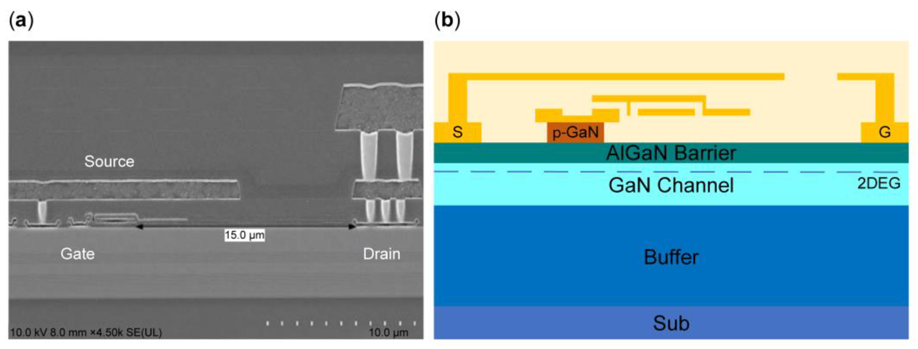
Figure 2.
Topology of UIS test circuit and test board, (a) UIS test circuit, (b) VGS waveform, (c) VDS, and IDS under UIS stress of Si/SiC MOS, (d) VDS and IDS under UIS stress of GaN HEMT, (e) the test board.
Figure 2.
Topology of UIS test circuit and test board, (a) UIS test circuit, (b) VGS waveform, (c) VDS, and IDS under UIS stress of Si/SiC MOS, (d) VDS and IDS under UIS stress of GaN HEMT, (e) the test board.
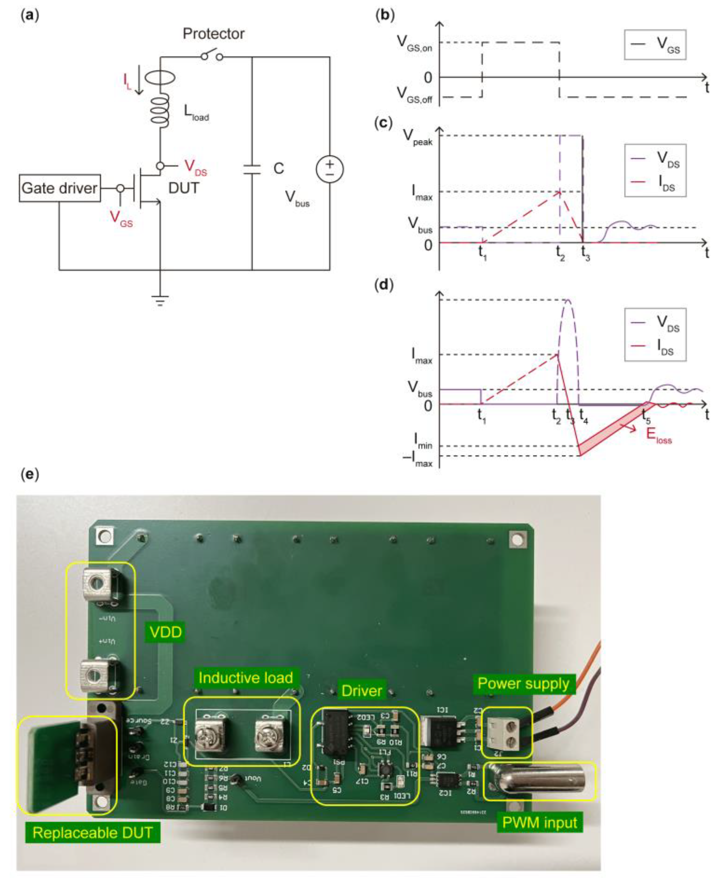
Figure 3.
Typical single-pulse UIS waveforms with load inductor of 0.3 mH at (a) the last test before failure; (b) at failure.
Figure 3.
Typical single-pulse UIS waveforms with load inductor of 0.3 mH at (a) the last test before failure; (b) at failure.
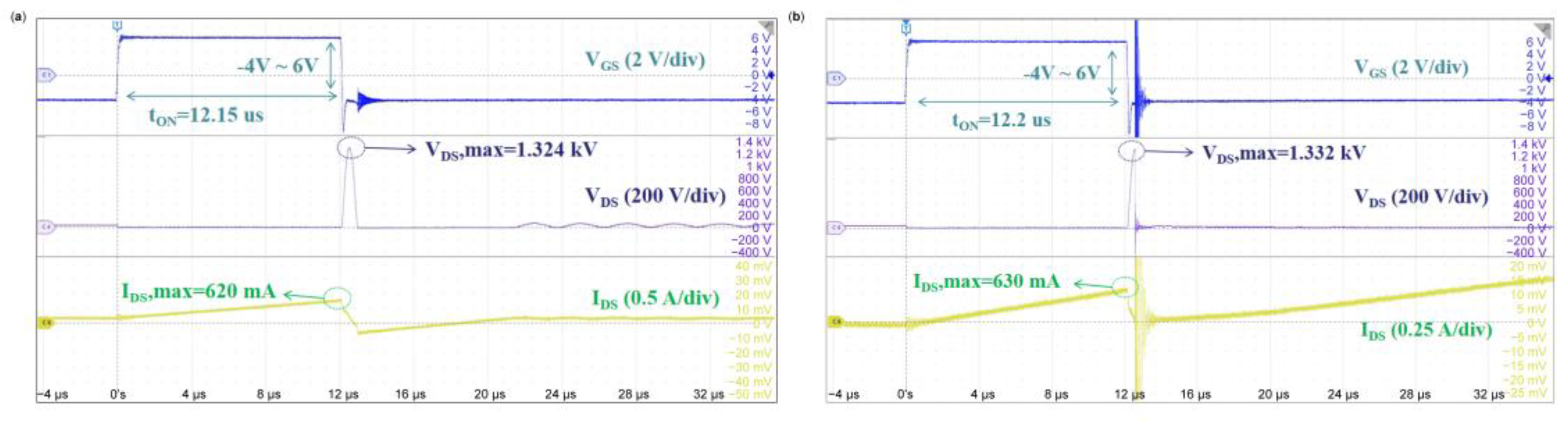
Figure 4.
Peak voltage versus peak current at single UIS test (a) different inductance; (b) at different Vgs_off; (c) at different temperature.
Figure 4.
Peak voltage versus peak current at single UIS test (a) different inductance; (b) at different Vgs_off; (c) at different temperature.
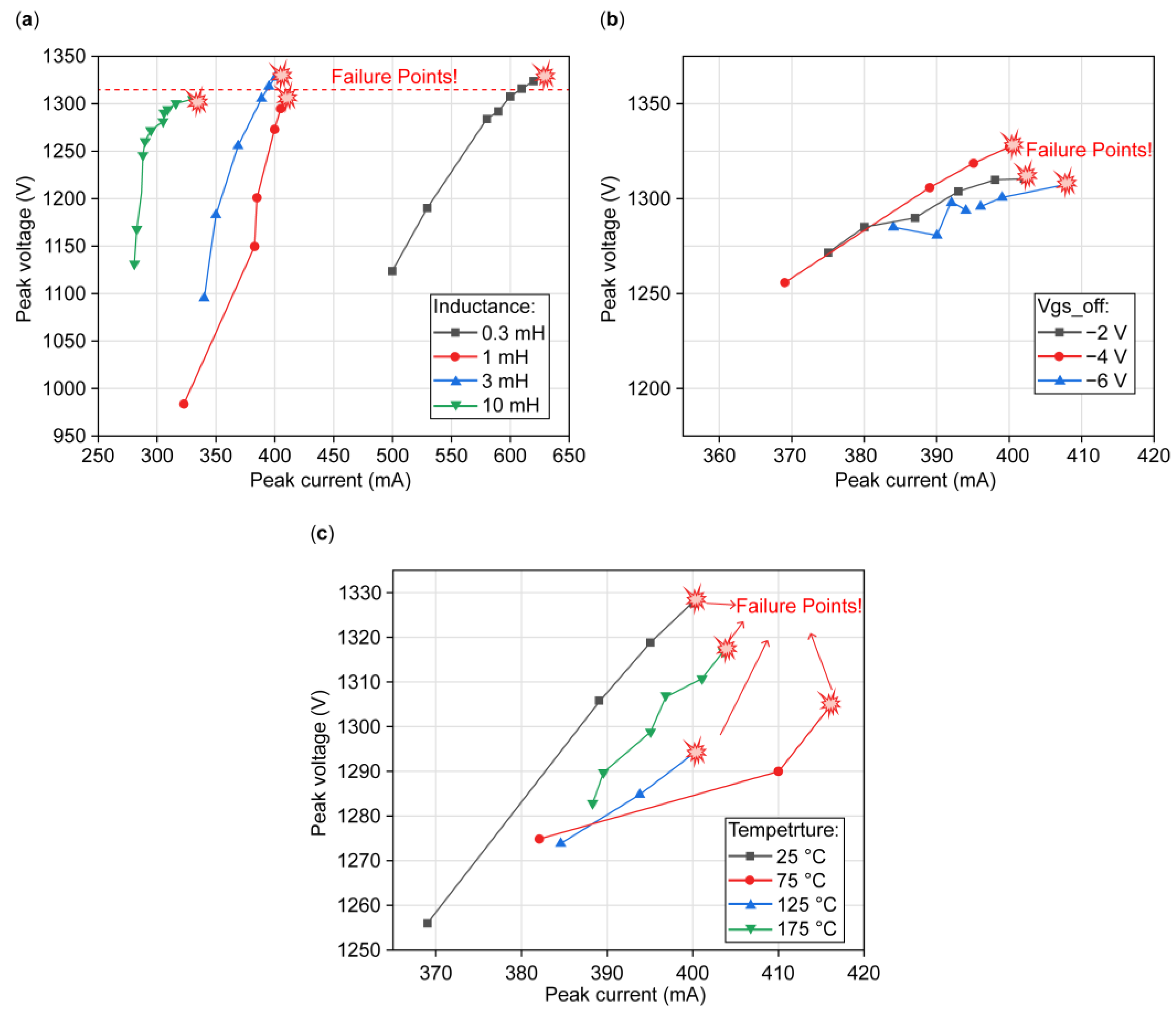
Figure 5.
Decapped failure samples and captured curves at failure: (a) decap failure point analysis of DUT ,(c) decap failure point analysis of DUT, (b) measured UIS waveforms when (a) failure occures: T=75°C, VGS= -4~6V,L=3 mH, VDD=30 V, (d) measured UIS waveforms when (b) failure occures: T=25°C, VGS= -4~6V, L=3 mH, VDD=30 V.
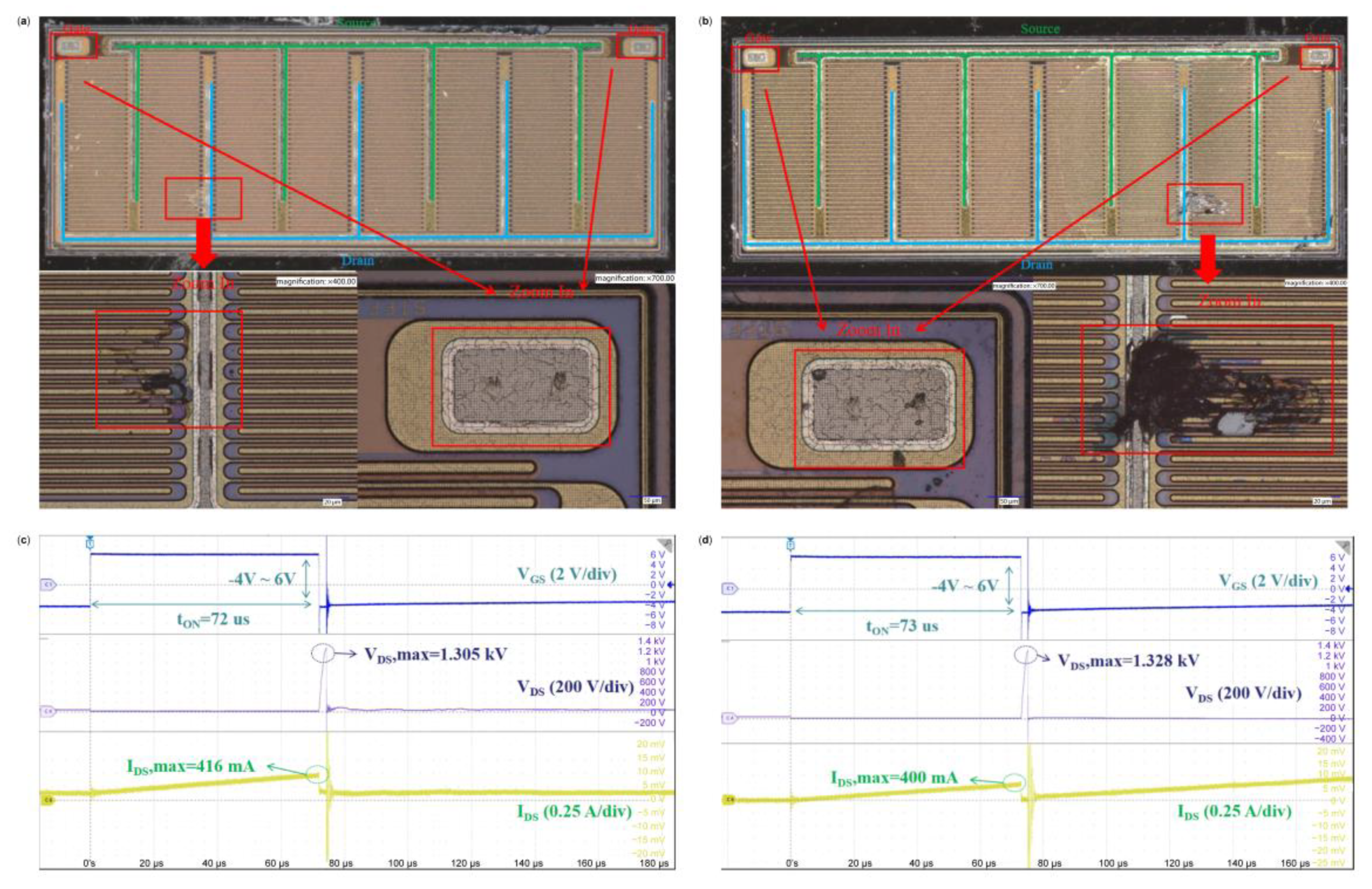
Figure 6.
Structure and simulated curves by TCAD, (a) cross section of DUT used in simulation, (b) simulated curves by TCAD.
Figure 6.
Structure and simulated curves by TCAD, (a) cross section of DUT used in simulation, (b) simulated curves by TCAD.
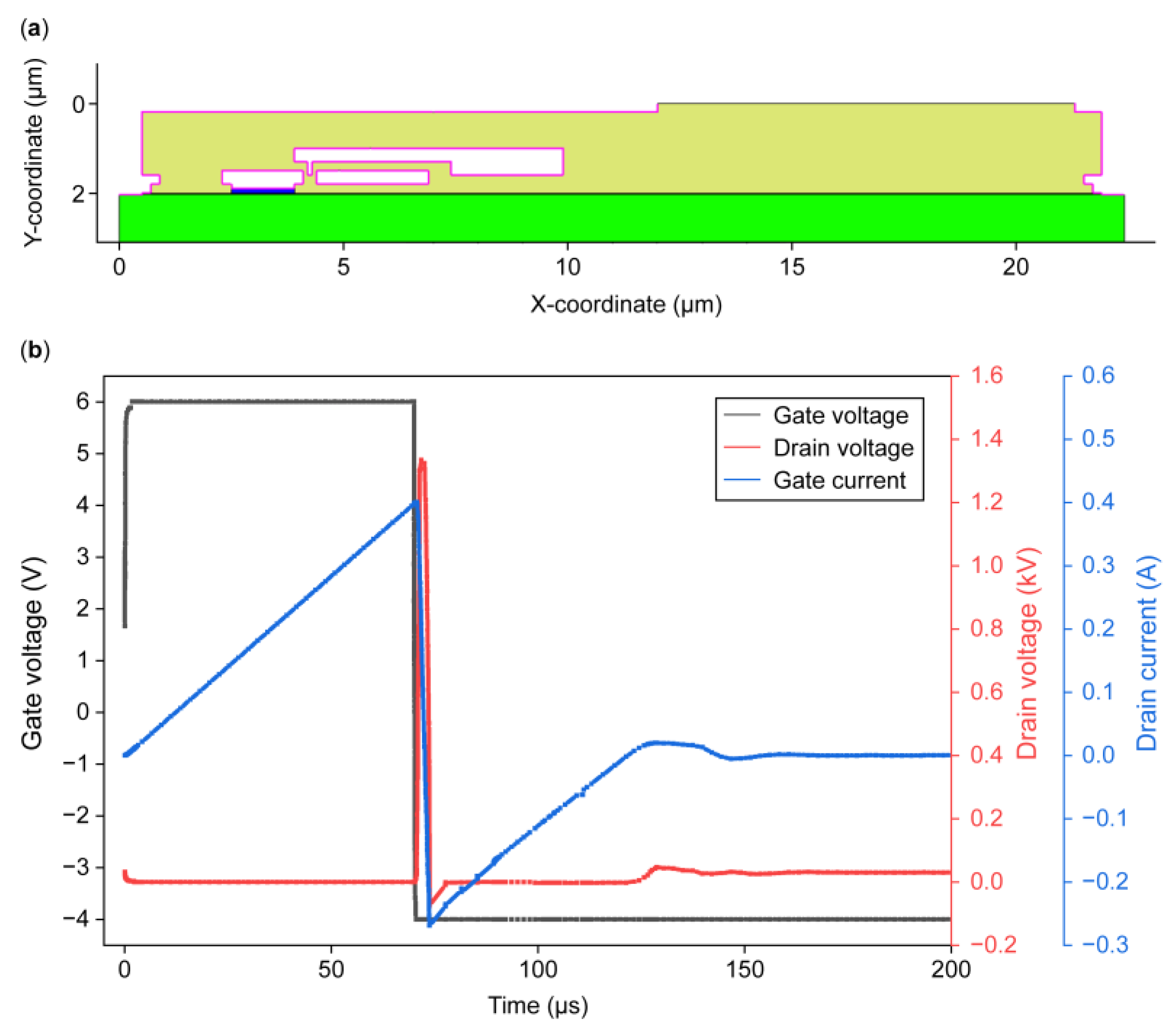
Figure 7.
Extracted profiles of DUT at peak voltage (a), electrical field and impaction ionization rate(I.I) (b), total current density (c), Electron current density (d), Hole current density.
Figure 7.
Extracted profiles of DUT at peak voltage (a), electrical field and impaction ionization rate(I.I) (b), total current density (c), Electron current density (d), Hole current density.
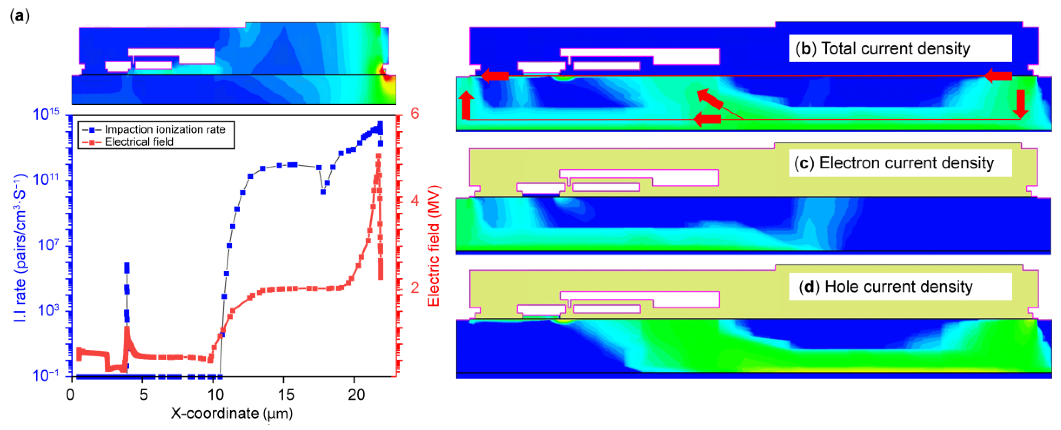
Figure 8.
Repetitive avalanche UIS test waveform diagrams.
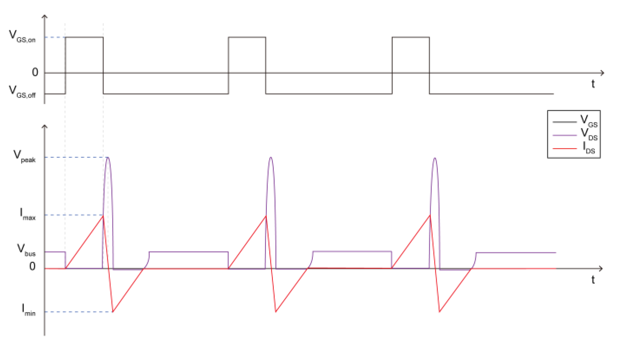
Figure 9.
Vth degradation versus cycles (a) measure instantly after cycles, (b) measure after 30min, (c) measure after 24hs lagging, (d) Vth degradation versus cycles.
Figure 9.
Vth degradation versus cycles (a) measure instantly after cycles, (b) measure after 30min, (c) measure after 24hs lagging, (d) Vth degradation versus cycles.
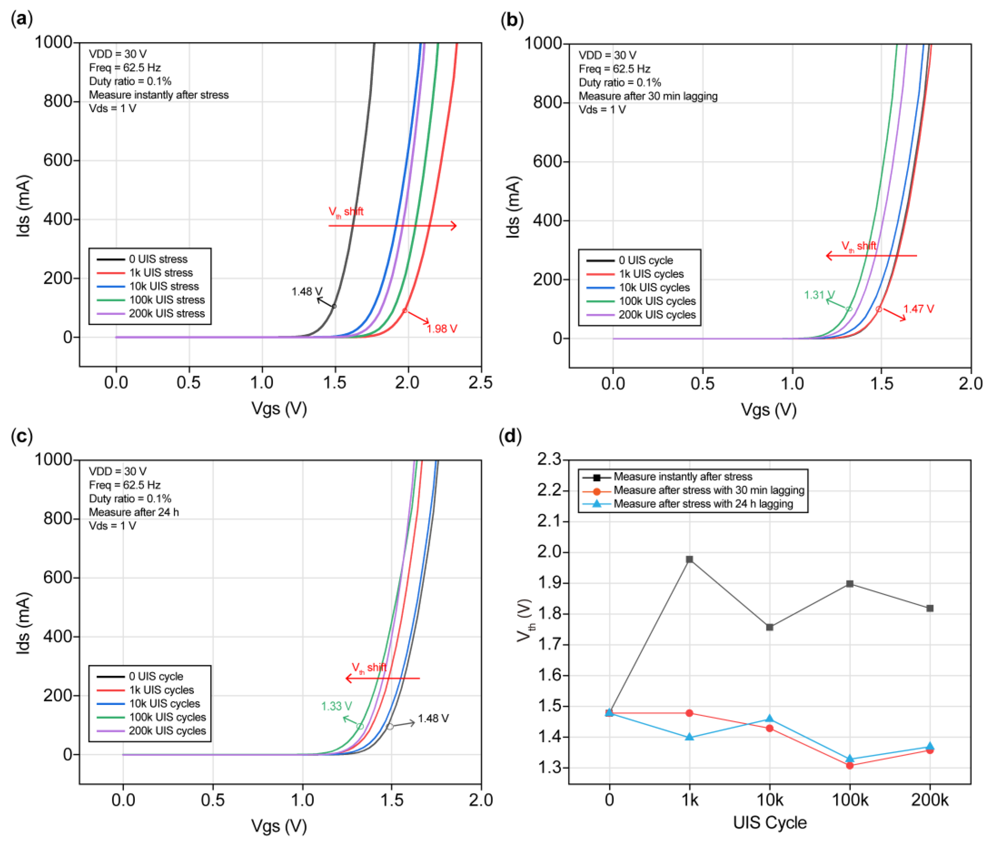
Figure 10.
Ron versus UIS cycles, (a) measure instantly after UIS cycles, (b) measure with 30mins lagging, (c) measure with 24hs lagging, (d) Ron versus UIS cycles.
Figure 10.
Ron versus UIS cycles, (a) measure instantly after UIS cycles, (b) measure with 30mins lagging, (c) measure with 24hs lagging, (d) Ron versus UIS cycles.
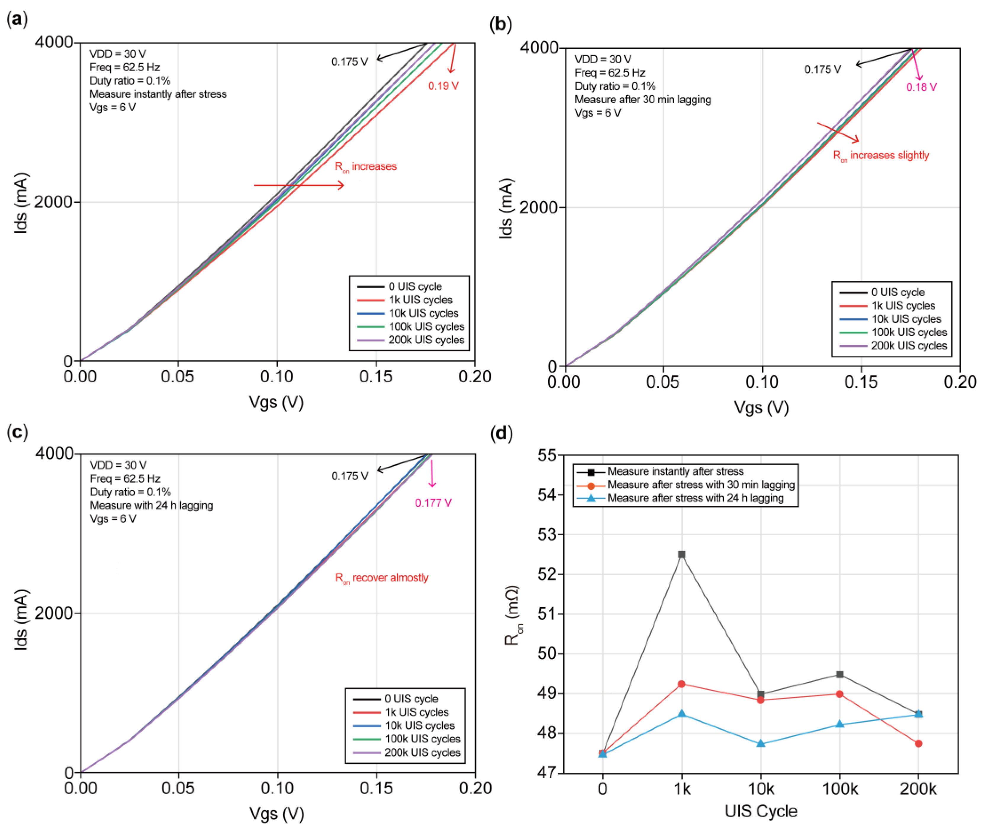
Figure 11.
Blocking characteristics under repetitive UIS stresses, (a) measure instantly after stresses, (b) measure with 30mins lagging, (c) measure with 24hs lagging, (d) BV versus UIS cycles.
Figure 11.
Blocking characteristics under repetitive UIS stresses, (a) measure instantly after stresses, (b) measure with 30mins lagging, (c) measure with 24hs lagging, (d) BV versus UIS cycles.
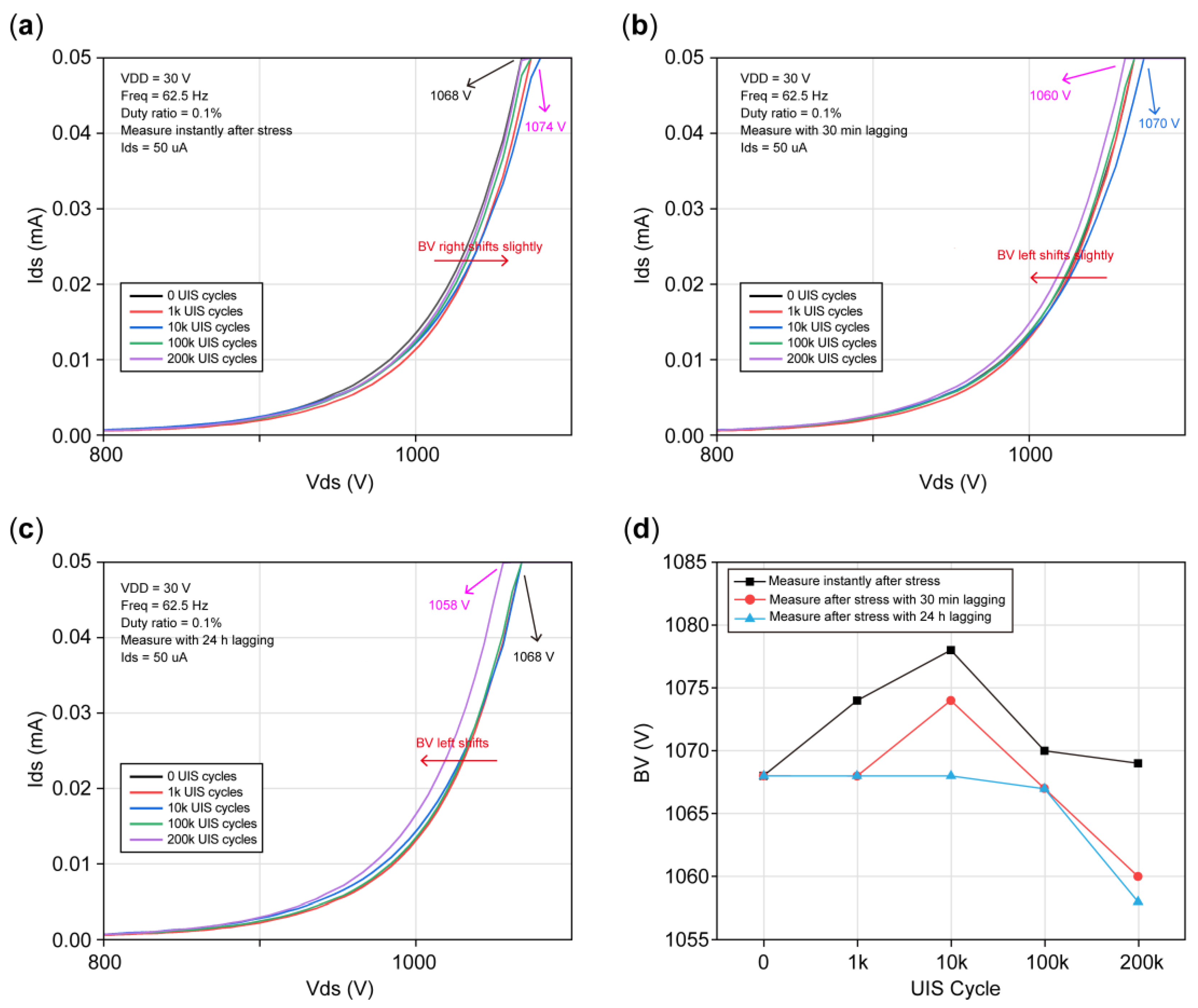
Figure 12.
gate leakage current degradation of GaN HEMT under repetitive UIS stresses, (a) measuring instantly after cycles, (b) measuring with 30mins lagging, (c) measuring with 24hs lagging, (d) Igss versus UIS cycles.
Figure 12.
gate leakage current degradation of GaN HEMT under repetitive UIS stresses, (a) measuring instantly after cycles, (b) measuring with 30mins lagging, (c) measuring with 24hs lagging, (d) Igss versus UIS cycles.
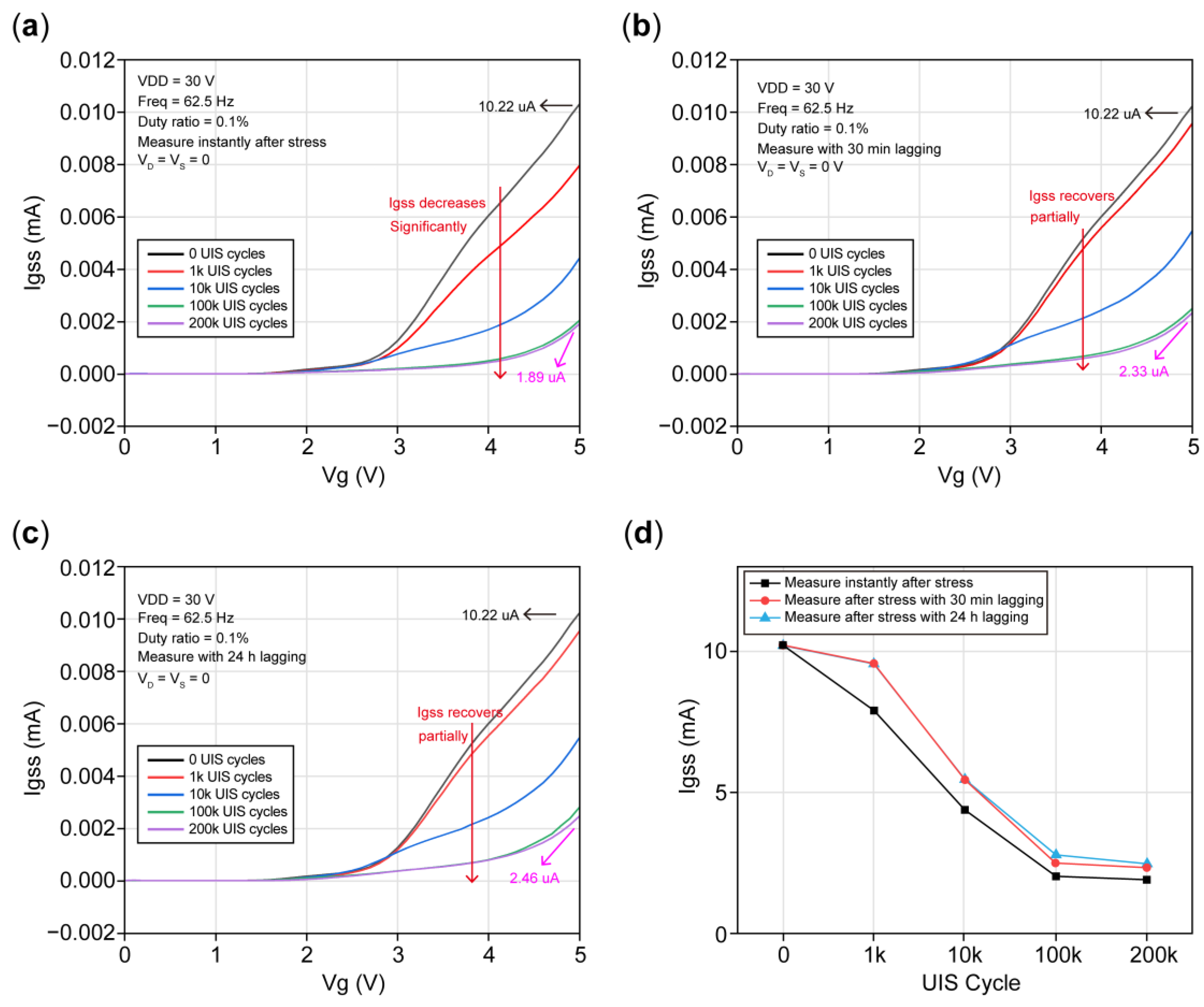
Figure 13.
Equivalent circuit of gate region in P-GaN HEMT.
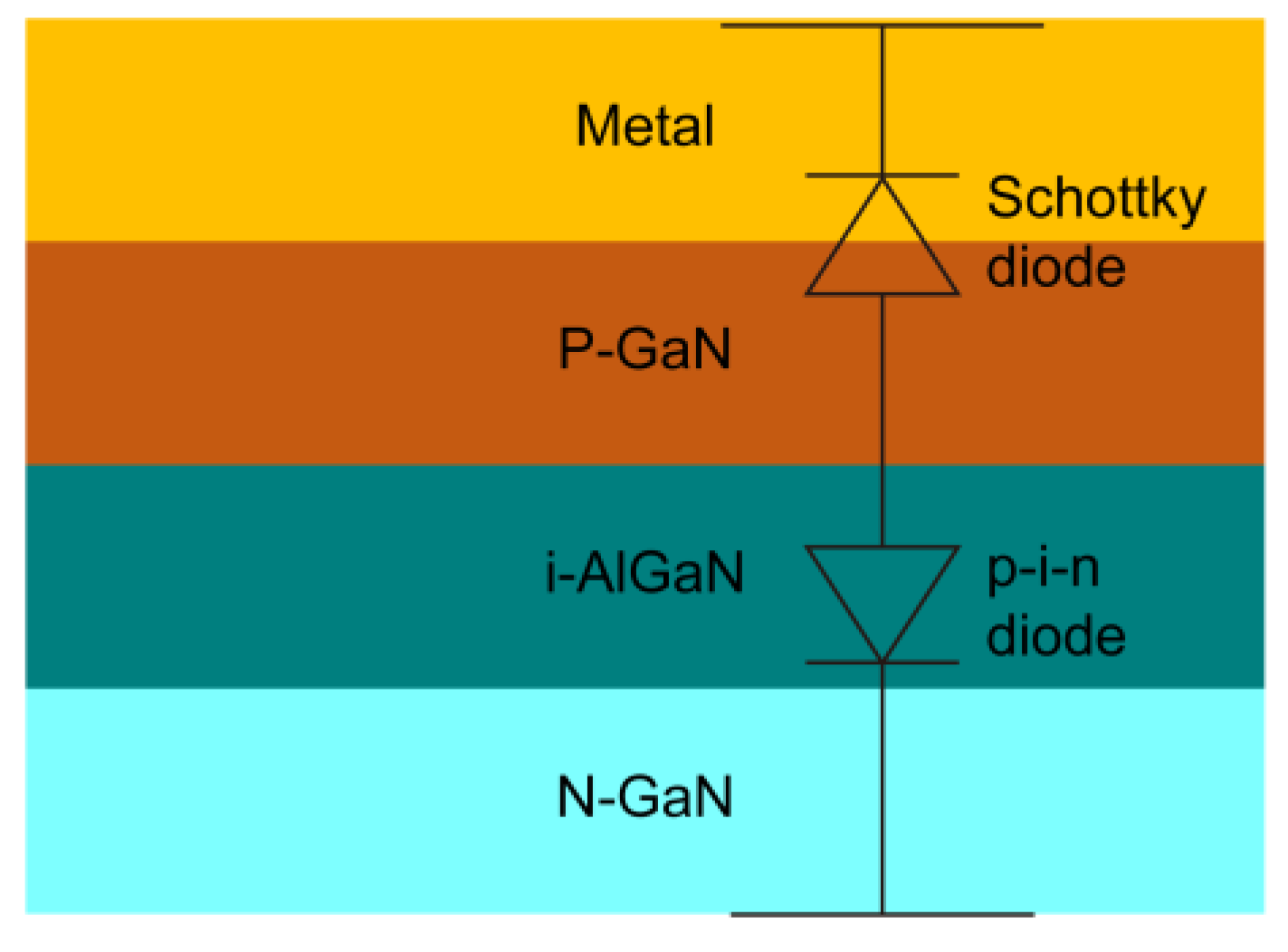
Figure 14.
charge transport when UIS occurs.
Disclaimer/Publisher’s Note: The statements, opinions and data contained in all publications are solely those of the individual author(s) and contributor(s) and not of MDPI and/or the editor(s). MDPI and/or the editor(s) disclaim responsibility for any injury to people or property resulting from any ideas, methods, instructions or products referred to in the content. |
© 2025 by the authors. Licensee MDPI, Basel, Switzerland. This article is an open access article distributed under the terms and conditions of the Creative Commons Attribution (CC BY) license (http://creativecommons.org/licenses/by/4.0/).
Copyright: This open access article is published under a Creative Commons CC BY 4.0 license, which permit the free download, distribution, and reuse, provided that the author and preprint are cited in any reuse.


