Submitted:
12 July 2023
Posted:
12 July 2023
You are already at the latest version
Abstract
In this work, we present an analytical model of dynamic power losses for enhancement-mode AlGaN/GaN high-electron-mobility transistor power devices (eGaN HEMTs).
To build this new model, the dynamic on-resistance (Rdson) is first accurately extracted by our ex-traction circuit based on a double-diode isolation (DDI) method for a high operating frequency up to 1 MHz and a large drain voltage up to 600 V, thus the unique problem of an increase in the dynamic Rdson is presented. Then the impact of the current operation mode on the on/off transi-tion time is evaluated by a dual-pulse-current-mode test (DPCT) which including a discontinu-ous conduction mode (DCM) and a continuous conduction mode (CCM), thus the transition time is revised for different current mode. Afterward the discrepancy between the drain current and the real channel current is qualitative investigated by an external shunt capacitance (ESC) meth-od, thus the losses due to device parasitic capacitance are also taken into account. After these improvements, the dynamic model will be more compatible for eGaN HEMTs.
Finally, the dynamic power losses calculated by this model are verified to be in good agreement with experimental results. Based on this model, we propose a superior solution with qua-si-resonant mode (QRM) to achieve lossless switching and accelerate switching speed.
Keywords:
AlGaN/GaN HEMT device
; CCM
; DCM
; dynamic on‐resistance
; dynamic power loss
1. Introduction
Enhancement-mode AlGaN/GaN high electron mobility transistor power devices (eGaN HEMTs) are the most promising candidates for next-generation power devices. In such devices, III-V materials have several merits due to their wide bandgap energy, high critical breakdown electric field, high electron mobility and capability [1,2], and polarization effect [3]. Because of these advantages, a high-frequency (high-fs) converter operating in the range of 1-5 MHz based on eGaN HEMTs can be readily realized. Although high-fs operation can help reduce converter size, it will generate more challenges with respect to dynamic power loss. Thus, building an analytical dynamic power loss model for an eGaN-based high- fs switch becomes important for prototype application circuit design.
Recently, some state-of-the-art dynamic power loss models for eGaN HEMTs have been proposed. Wang et al. developed two analytical loss models based on detailed parasitic parameters for high-voltage and low-voltage GaN eHEMTs [4,5]. In these models, the gate charge (Qg) and output charge (Qoss) instead of the voltage-dependent capacitance were used to improve the nonlinear characteristics. Shen et al. fully accounted for the effects of parasitic parameters and transconductance [6]. Hou et al. and Guacci et al. investigated the losses caused by output capacitance in a hard switch and soft switch, respectively [7,8]. However, these models did take into account the impact on device loss from some aspects instead of fully evaluated, the results accuracy is affected.
Chen et al. presented a complete analytical loss model for low-voltage eGaN HEMTs, which a piecewise model was employed [9]. Piecewise models are also usually used to evaluate the dynamic power losses for Si- and SiC-based metal-oxide-semiconductor field-effect transistors (MOSFETs) [10,11,12,13,14,15]. These models are carefully considered and allow accurate evaluation of device power losses. However, these models did not take into account the exclusive dynamic physical characteristics of eGaN HEMTs, such as a strong defect trapping-effect, increased dynamic on-resistance (Rdson), and no reverse body diode. Therefore, these analytical models need to be modified for eGaN HEMTs. In addition, the effect of current operation mode on device transition time and loss is not considered in all known device loss models.
To improve the dynamic power loss model of eGaN HEMTs, we propose three experimental methods according to the practical application of devices in high-fs circuits, such as a double-diode isolation (DDI) method, a dual-pulse-current-mode test (DPCT) method, and an external shunt capacitance (ESC) method. Then, the dynamic Rdson is accurately extracted in a high operating frequency (fs) up to 1 MHz and a high drain voltage up to 600 V; the effect of current operation mode on transition time is revealed for the first time and thus the loss of the device is affected; and the real channel current (Ich) is qualitative modified compared to the drain current (Idrain) we can directly test in device drain side. Afterward the dynamic power loss of eGaN HEMTs is carefully described by a modified 12-segment piecewise model. Finally, we propose a quasi-resonant mode (QRM) with a low off-state drain voltage (Vds_off), zero turn-on current, and a relatively large on-state peak current for a lossless design and fast transit speed in power switches.
2. Background And Methodology
2.1. A. Parameters and Traditional Power Loss Model
: gate voltage.
: gate voltage in high level.
: gate voltage in low level.
: Miller gate voltages during the turn-on transition.
: Miller gate voltages during the turn-off transition.
: threshold voltage.
: total turn-on time during the turn-on transition.
: turn-on delay time.
: turn-on current rise time.
: turn-on voltage fall time.
: turn-on Miller rise time.
: turn-on gate voltage rise remaining time.
: total turn-off time during the turn-off transition.
: turn-off delay time.
: Miller fall time.
: voltage rise time.
: current fall time.
: voltage continuous rise time.
: gate-source charge.
: gate-drain charge.
: overcharge gate charge.
: total gate charge, equal to the sum of Qgs, Qgd, and Qod.
: drain-source current.
: start drain-source current at turn-on transition.
: peak drain-source current during on-state.
: drain-source voltage.
In the piecewise model, the operating sequence of the device is shown in Figure 1. In particular, the device is usually connected to a choke or a transformer in power switches, thus the value of Ista indicate the current mode of device. (Ista=0) denotes the device operate in discontinuous conduction mode (DCM), while (Ista>0) denotes the device operate in continuous conduction mode (CCM).
A traditional calculation formula for high-fs power losses of device is given by [16]
where Idson_rms is the on-state drain-source current in root-mean-square (RMS) value, Kth is the temperature coefficients related to Rdson. The first term in Eq. (1) occurs in the crossing area of Ids and the Vds, while the second term is the output capacitor energy dissipated in the device during the turn-on transition. Then, the third and fourth terms are the conductive loss and driving loss, respectively. Equation (1) is approximate, as it does not take into account the problem of a dynamic Rdson increase, the impact of Idrain on the transition time, and the discrepancy between Idrain and the real channel current.
2.2. B. Experimental Circuit and Method
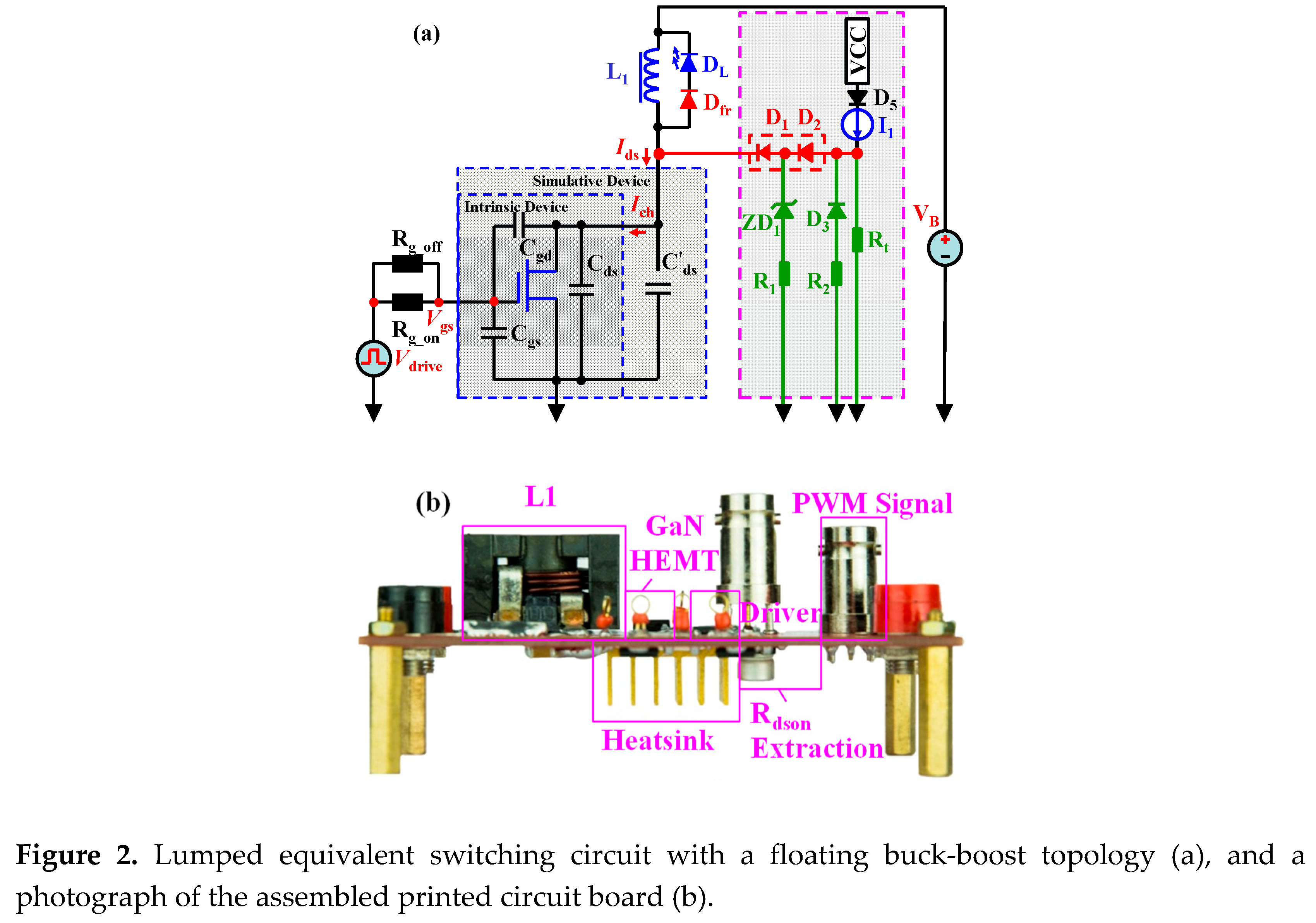
A switching circuit with a floating buck-boost topology is employed to analyze the switching processes, as shown in Figure 1a. In this circuit, an HEMT device is used and shown with a simple three-capacitor model that includes the parasitic capacitors Cgs, Cgd and Cds. The pulse width modulation (PWM) is produced by a pulse generator (81150A, Keysight Inc.) with a maximum PWM of 120 MHz, and is amplified by a gate driver (SI8271GB), which has a 1.8 A peak source current and a 4.0 A peak sink current, D1 is selected as a SiC diode (C3D10065E) rated at 15 A / 650 V, which is used to reduce the reverse recovery problem. The parasitic resistor and parasitic inductor are ignored to simply study the important role of the parasitic capacitors at a relatively high-fs that is smaller than 30 MHz. Then, various voltages and PWM in DCM and CCM are applied to elucidate the switching processes and the production of dynamic power losses.
Figure 1b shows our novel dynamic Rdson extraction circuit [17]. In this design, the model of the gate driver is SI8271GB, and D1 and D2 (1 A/1k V UF4007) are used in series to isolate the high off-state voltage of the eGaN HEMTs. Then, the dynamic Rdson of the eGaN HEMTs can be easily extracted. Diodes in series make it possible to test the real-time forward voltage drop (VF) of D2 in a low-voltage range and then to precisely estimate VF of D1 in the same forward current. In addition, diodes in series will reduce the parasitic capacitor by half, which is very helpful to the high-fs response of the extraction circuit. We call this method a DDI method. Moreover, ZD1 and D3 are freewheeling diodes and ZD1 is also a positive clamping diode. These two diodes are a general 5 V Zener ZD1 and a general small signal diode D3 (1N4148) with 75 V/150 mA. All of the functional diodes including D1, D2, ZD1 and D3 are specially selected with a very low parasitic capacitance, which will improve the high-fs response of the extraction circuit to several MHz. I1 is a constant-current source of only several mA, so it cannot produce a temperature problem and an extra self-heating effect. I1 consists of a constant-current diode, which is actually a junction field transistor with a gate-source short connection. Therefore, I1 can achieve an excellent constant current over a wide operating voltage range. Rt provides a minimum load for I1 and suppresses the voltage spike at point B. An isolated low-voltage probe (P2221 from Keysight Inc.) with a 1:1 attenuation can be used to test VF of D2 and the voltage at point B. The low-voltage probe with a 1:1 attenuation will not amplify the background noise and operate in a low-voltage range, so it can obtain an improved test accuracy.
We build the above switching circuit and extraction circuit with one printed circuit board (PCB), as shown in Figure 1c.
2.3. C. Qualitative Method to Discover the Channel Behavior
Since we cannot perform the measurements inside the HEMT device directly, we propose a new evaluation method by employing an extended parallel capacitor Cds’, as shown in Figure 3. In this lumped circuit, the intrinsic capacitor Cds is assumed to not exist, and the extended capacitor Cds’ outside the device is assumed to be the intrinsic capacitor. Therefore, the channel current (Ichannel) and Idrain can be measured directly and separately by an oscilloscope and current probes. Although an extra parallel capacitor will lead to an increase in the measured Idrain and Ichannel, this qualitative method can be used to assess the difference between these two currents, and thereby, the cause of the discrepancy can be located. After understanding this reason, the resulting loss effect on the eGaN HEMT device can be further quantified by an analytical method. In the analytical method, the additional Cds’ is no longer required, therefore, the Cds’ does not materially affect the device losses.
3. Extraction of the Dynamic Rdson
It is well known that a high Vds_off will cause surface- and buffer-related trapping processes, which will lead to a larger dynamic Rdson compared to the direct current (DC) Rdson (Rdson_DC) [18,19]. Figure 4 illustrates the mechanism of the increase in the dynamic Rdson induced by the trapping effect. The high electric field helps the electrons escape from the GaN well, and then these electrons are captured by traps or some of the surface states that are activated by a high electric field. When removing the electric field, these trapped electrons cannot be released to the well instantaneously. The reason for the slow return of electrons is that the trapping time of electrons in the off-state is on the order of ns, whereas the detrapping time of electrons in the on-state is on the order of second [20,21]. Thus, trapped electrons accumulate and worsen the device performance at a high fs. Meanwhile, electrons migrate from the gate to the gate-drain side adjacent surface to form a virtue gate; hence, the number of electrons in the access region decreases. The decreasing number of electrons in the drift region will result in a large dynamic Rdson [22,23].
In the circuit of Figure 1b, the current I1 flows partly through Rt and partly through the HEMT device, and the voltage of point B (VB) can be tested by the voltage probe P2221 directly. Then, the dynamic Rdson can be calculated by
where , , , , and I1 are the average voltages of point B and D2, the average currents through a resistive load and D2, and the current of the constant-current supply, respectively. Idrain, the voltage of point A (Vdrain) and VF_D2 of D2 are tested by a current probe (TCP0020), a high-voltage differential probe (THDP0200), and a low-voltage differential probe with a 1:1 attenuation (TIVH02) and displayed on an oscilloscope (MDO3104). Finally, the calculated dynamic Rdson is normalized by Rdson_DC, which is 200 , from an eGaN HEMT (GS66502B from GaN Systems Inc.) [24].
Figure 5b–f show the results of the dynamic Rdson of the eGaN HEMT for various Vds_off, fs, duty cycles, Idrain and operating temperatures, which are extracted in the on-state by taking average values in the stable region marked in Figure 5a,b shows that the dynamic Rdson increases as Vdrain increases, under the conditions of an 80% duty cycle and an fs of 100 kHz, so the dynamic Rdson is voltage-dependent. Figure 5c,d show the dynamic Rdson increases as fs increases and duty cycle decreases, respectively for a 500 V Vdrain condition, so the dynamic Rdson is also time-dependent. Considering that the dynamic Rdson is not only affected by the trapping effect, we further test the relationship between the dynamic Rdson and Idrain and temperature, as shown in Figure 5e,f, respectively. These two tests will help us isolate the trapping effect caused by the increase in the dynamic Rdson in a particular complex test condition.
In conclusion, the trend of the results of the extracted dynamic Rdson of the eGaN HEMT is consistent with the mechanism of the trapping-effect-induced increase in the dynamic Rdson. From Figure 6, we can obtain the real conduction resistance of the eGaN HEMT device under a certain working condition, and then the conduction loss can be corrected.
4. Discussion on the Effect of the Drain Current by a Double-Mode Test Technique
Base on the test circuit in Figure 1, a new double-mode test technique which including a DCM and a CCM is proposed. Then, the tested waveforms during the turn-on and turn-off transitions for various voltage and PWM conditions are illustrated in the Figure 6. To ensure that the switching circuit operates in open-loop CCM and DCM, VBulk is set to 400 V, and the VLoad is set to 80 V in DCM and 20 V in CCM, so the Vds_off values of the devices in the two modes are different.
The current Idrain in DCM exhibits only one resonant waveform when the drain voltage decreases, as shown in Figure 6a, while Idrain in CCM has an extra linear increase before the resonant waveform occurs, as shown in Figure 5b. The corresponding voltage fall time is approximately 14 ns in Figure 6(a) and is approximately 42 ns in Figure 6b, so that the extra linear increase in the current will increase the turn-on time and cause a high dynamic power loss. This linear increase in the current is caused by the high start current and the linear conduction of the eGaN HEM at this time. This means that DCM is a better operating mode for reducing the turn-on time.
In addition, the rise time of the drain voltage during the turn-off transition, which is approximately 10 ns, as shown in Figure 6d, is faster than that of approximately 30 ns in Figure 6c. This is because Idrain in Figure 6d is higher than that in Figure 6c, and the rise time of the drain voltage during the turn-off transition mainly depends on the charge time of Coss. Moreover, the peak current in DCM during the turn-off transition will be higher than that in CCM under the same output power conditions. This means that DCM is a better operating mode for reducing the turn-off time.
In conclusion, the drain current will significantly affect the turn-on and turn-off times, and DCM is better than CCM for reducing the crossover power losses.
5. Investigation on the Real Channel Current
According to the qualitative method in Figure 2, we can study the discrepancy between Idrain and Ichannel. Figure 7a shows the tested Idrain, Ichannel, Vdrain and Vdrive values of the AlGaN/GaN HEMT in the turn-on transition for a Vds_off of 500V, an fs of 100 kHz, and a duty cycle of 16.5%. It is shown that Ichannel is larger than Idrain while the drain voltage decreases. The current path in this time interval is shown in Figure 7b, where the channel current partially results from the discharging current of the parasitic output capacitor.
Figure 7c shows the tested Idrain, Ichannel, Vdrain and Vdrive values of the AlGaN/GaN HEMT during the turn-off transition for a Vds_off of 500 V, an fs of 100 kHz, and a duty cycle of 16.5%. It is shown that Ichannel is smaller than Idrain while the drain voltage increases. The current path in this time interval is shown in Figure 7d where the channel current is partially diverted to the branch of output capacitor.
In conclusion, Ichannel is not exactly equal to Idrain, and unfortunately, Ichannel cannot be tested directly. However, with the above test results and the current path analysis, we can acquire the reason for the discrepancy between Ichannel and Idrain so that the real Ichannel value can be obtained by a test of Idrain and an analytical method, and the power losses of eGaN HEMTs can be correctly evaluated.
6. Modeling of Switching Power Losses
Figure 8 shows a detailed timing diagram of the switching period [25] for eGaN HEMTs in DCM or CCM. The operating period of the power devices can be divided into 12-time intervals from t0 to t12 according to the status of the drain voltage and Idrain in the off-state, on-state, turn-on transition, and turn-off transition. To investigate the detailed dynamic power loss, we reclassify the 12-time intervals into the following four stages (S1-S4) according to their different contributions to the dynamic power loss.
6.1. A. Stage 1(S1) – Off-state with a High Vds
During the t0–t1, t10–t11time intervals and the time of the off-state, the device sustains a high Vds. Thus, the voltage-dependent leakage current (Ilk) will lead to an off-state power loss (Poff). We can no longer ignore this power loss, especially at a very high drain voltage and a very high frequency. In general, the t0–t1 and t10–t11time intervals can be neglected in comparison with the off-state time, so Poff can be written as
where T and D are the period and duty cycle, respectively. In addition, eGaN HEMTs have no reverse recovery problem because the 2DEG in the channel is naturally formed by the polarization effect. This will reduce the power loss and mitigate the electromagnetic interference (EMI) problem which is produced by the reverse recovery caused by ringing.
6.2. B. Stage 2(S2) – On-state in Saturation Region
During the t4–t7 time intervals, the device is in the on-state. The RMS value of the drain current (Idrain_rms) can be written as
To take the problem of the increase in the dynamic Rdson into account, the traditional conductive power loss (Pcon) can be modified by
where ,,,andare the dynamic coefficients of Rdson related to the voltage, fs, the duty cycle, the current and the temperature, respectively.
6.3. C. Stage 3(S3) – Turn-on Transition
During the t1–t4 time interval, the device is in turn-on transition. In the t1–t2 time interval, Idrain increases while Vdrain decreases slightly in CCM, but this time interval does not exist in DCM; in the t2–t3 time interval, Vdrain decreases and leads to a resonant Idrain; in the t3–t4 time intervals, Vdrain decreases to very low voltage, and the device starts to operate in an ohmic conducting state. These crossovers of Vdrain and Idrain will cause power losses during the turn-on transition (Pturn_on):
- 1)
- In the t1–t2 time interval, Idrain increases almost linearly from 0 to theat t2, similar to a Si-based MOSFET [26,27], while Vdrain decreases slightly from Vds to Vr due to the result of the parasitic inductance voltage drop caused by a high di/dt in the circuit. At t2, the current of the freewheeling diode D1 decreases to zero. In this time interval, the gate voltage of the device slightly exceeds Vth, so the device is operating in a linear region. Meanwhile, the trapping effect for a high electric field will also lead to a large dynamic Rdson in the linear region (Rturn_on_cr), similar to that in the on-state, as well as an extra gate lag. Thus, the coefficients of the dynamic Rdson should be the same as those in Figure 4. Assuming that the heatsink is large enough and the self-heating effect is ignored, the t1-t2 time interval, Vr and the power losses in this time interval (Pturn_on_cr) can be written by
- 2)
- In the t2–t3 t.ime interval, the HEMT device takes over the total inductive load current, and Vds decreases to a boundary voltage of (Vmr-Vth) at t3 due to the discharging of Coss. The stray inductors in series around the circuit are resonant with Coss and the stray capacitors (Cstray) in this time interval. The current path through the device is illustrated in Figure 5b. It is assumed here that Vgs and ista remain unchanged, and the reverse recovery of the D1 is zero. In addition, the current in this time interval is usually large enough; and hence, the charging time of Coss can be ignored. Moreover, voltage-dependent Coss is not suitable for calculating power losses in this time interval because Vdrain is always changing. Therefore, Qgd is used to replace Coss, and then the time interval of t2-t3 can be written as
Then, the power losses in this time interval (Pturn_on_vf) can be written by [28]:
where is the average channel current during the t2–t3 time interval.
- 3)
- During the t3–t4 time interval, the HEMT device operates in an ohmic conducting state. Then, Vdrain continues to decrease until it reaches a low on-voltage (Von) from(Vmr-Vth). Assuming that ista and the Miller voltage Vmr do not change, then the t3-t4 time interval, Von_r and the power losses in this time interval (Pturn_on_mr) can be written by [29]:
From the above analysis, Equation (6) can be modified by
Notice that in this stage, ista is a tested drain current instead of a real channel current and they are actually different in the t2–t3 time interval, as shown in Figure 5a. However, Ichannel is the real factor that results in the power losses in this stage, and the real Ichannel is the combined current of Idrain and the discharging current of Coss:
Thus, Equation (18) can be finally modified by [12]
Where
Thus,
6.4. D. Stage 4(S4) – Turn-off Transition
During the t7–t11 time intervals, the device is in a turn-off transition. In the t7-t8 time intervals, the drain voltage increases while Idrain stays almost constant; in the t8–t9 time intervals, the drain voltage continuously increases while Idrain decreases slightly; in the t9–t10 time intervals, Idrain decreases while the drain voltage stays almost constant. Finally, Idrain decreases to zero, and the drain voltage becomes resonant in the t10–t11 time intervals. These crossovers of Vdrain and Idrain will cause power losses during the turn-off transition (Pturn_off):
- 4)
- In the t7–t8 time interval, the observations are very similar to those in the t3–t4 time interval. The HEMT device goes into a linear region from an ohmic conducting state. Vdrain increases to a boundary voltage of . Assuming that the peak current is unchanged, and , then the t7-t8 time interval, Von_f and the power losses in this time interval (Pturn_on_mf) can be written by:
- 5)
- In the t8–t9 time interval, the observations are very similar to those in the t2–t3 time intervals. Vdrain continues to increase faster towards the off-state Vds_off, while Idrain decreases slightly to ir. This current drop is caused by a charging shunt to other peripheral devices [25], and the current path through the device is illustrated in Figure 5d. Assuming that the Miller voltage (Vmf) remains unchanged and that the current-dependent charging time of Coss can no longer be ignored, we have:
- 6)
- In the t9–t10 time interval, the observations are similar to those in the t1–t2 time interval. Idrain decreases from ir to a low value because the current begins to divert from the HEMT device to D1. In this time interval, the drain voltage is in a state of resonance, while Vgs decreases to (Vmr-Vth) and the device channel current reaches zero at t10 [30]. Then, the t9-t10 time interval and the power losses at this time interval (Pturn_off_cf) can be written by:
- 7)
- During the t10–t11 time interval, the device is turned off but Vdrain ringing occurs due to the resonance between Coss and Lstray. These fluctuations of the drain voltage will lead to a slight power loss which depends on the ringing peak voltage (Vds_pk). Assuming that the reverse recovery of D1 is zero, we have:
From the above analysis, Equation (23) can be modified by
instead of real channel currents and they are actually different in the t8–t9 time interval, as shown in Figure 5c. However, Ichannel is the real factor that results in the power losses in this stage, and the real Ichannel is the diverted current of Idrain and the charging current of Coss:
Thus,
Finally, the total power loss (Ptotal) should be described with the sum of Equations (3)–(38):
In particular, the effects of Ichannel and Idrain on Ptotal can finally cancel out for a hard switch. However, in a soft switch application such as a zero-voltage switch (ZVS), is zero; hence,can no longer cancel out. This correction becomes very meaningful to the universality of the dynamic power loss model for eGaN HEMTs.
As can be seen, Ptotal in Equation (39) is very different from that in Equation (1). Equation (39) has no power loss of reverse recovery, but it takes the trapping-effect-induced dynamic Rdson and the impacts of the Idrain and the real Ichannel into account.
7. Model Verification by Experiments
To verify our dynamic power loss model, we adopt a floating buck-boost power converter with a light-emitting diodes (LEDs) operating in DCM and CCMs. To maintain the operation mode and the output current (Io) in an open-loop control system, some key parameters are adjusted (such as L1) or tested (such as the output voltage Vo, peak operating current Ipk, and the output power Po) in the circuit, as shown in Figure 8, for an input voltage (VBulk) of 400 V, a duty cycle of 10%, and various fs and Io values.
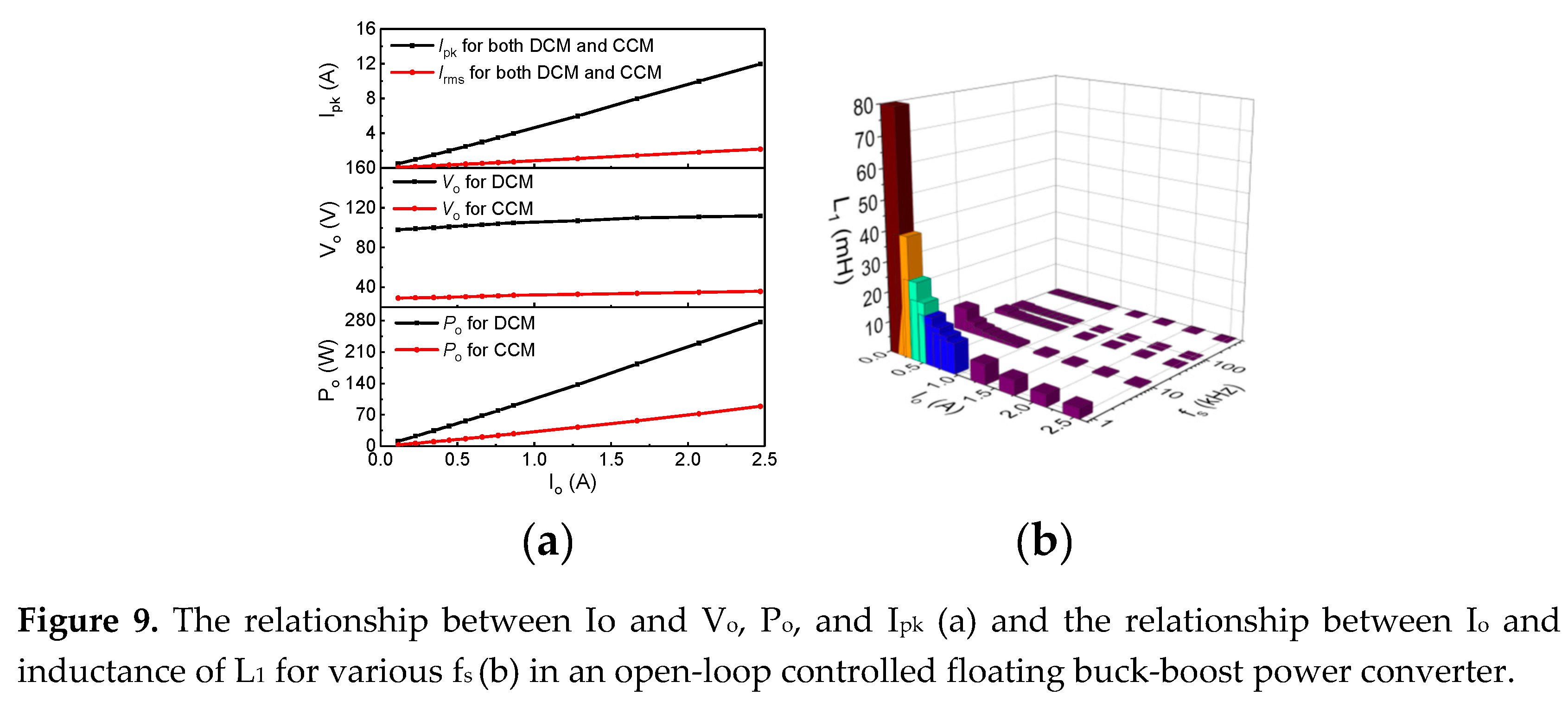
The power losses are then tested by a power analyzer (PW6001-03 from HIOKI Inc.). Figure 10a–c reveal that the analytical results of the total dynamic power losses by the proposed model are in good agreement with experimental results both in CCM and DCMs, even for various Io, fs and VBulk values. The experimental results are slightly different from the analytical results, which may be because of the measurement accuracy of the power meter reduced at a high fs.
Figure 11a shows the relationship between the total dynamic power losses and Io in CCM and DCMs. In the case of a small Io, the switching loss is dominant, while in the case of a large Io, the conduction loss is dominant. In addition, the dynamic power loss increases faster with the increase in Io in DCM than in CCM, indicating that DCM is not suitable for high current conditions.
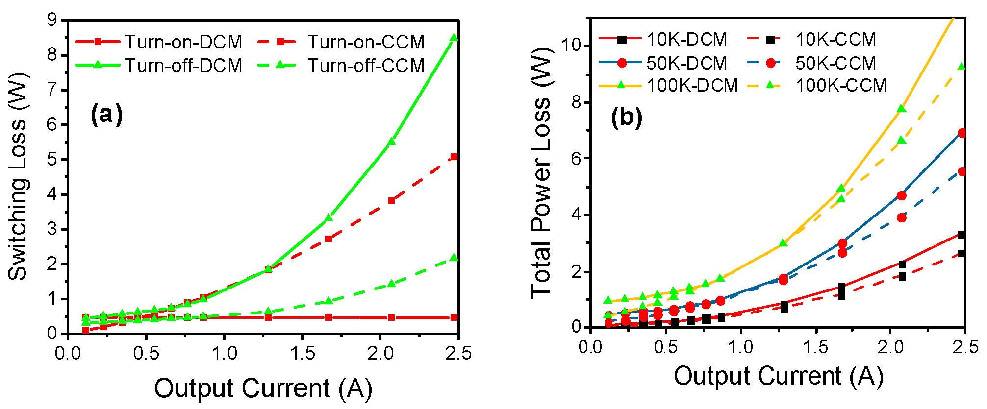
Figure 11b shows the switching loss during the turn-on and turn-off transitions in CCM and DCM. The results reveal that the switching loss is lower in DCM than in CCM during the turn-on transition but larger during the turn-off transition when Io is larger than 1.25 A. This means that DCM is more suitable for a relatively small Io. In this case, from Figures 10b and Figure 11a, 1.25 A is a moderate output current that is acceptable.
To restrain the peak current and obtain a high operating efficiency, the QRM is then proposed. The reason is that QRM works at the DCM boundary, where Vdrain will decrease to a minimum value at the beginning of the turn-on transition while Idrain decreases to zero. In addition, the peak on-state current in DCM is usually larger than that in CCM, and the current will be at a controllable high level, so the turn-off time is fast in QRM. Therefore, QRM is more suitable for achieving a lossless switch and even for reducing the turn-off transition time.
8. Conclusions
An improved 12-time-interval piecewise dynamic power loss model for eGaN HEMTs is developed by specially quantifying the effects of the increase in the dynamic Rdson, the impact of Idrain on the turn-on and turn-off times, and the real Ichannel, good agreement with some experimental results is verified.
In this work, three new methods or techniques are proposed, which are DDI method, double-mode test technique and qualitative, respectively. Then, the dynamic Rdson is obtained by our new extraction circuit at a high operating fs up to 1 MHz and high drain voltage up to 600 V, and the drain current is found to significantly affect the turn-on and turn-off times by a switching circuit operating in DCM and CCM, and the real channel current is accurately calculated to distinguish it from the measured drain current. All of these parameters are included into the power loss model.
Moreover, the QRM has a low Vds_off, zero turn-on current, and relatively large peak current. Therefore, on the basis of the model, we propose the QRM to obtain a high efficiency and decrease the turn-off switching time for the application of eGaN HEMTs.
Author Contributions
Funding acquisition, Liang Xu and Jing Yu; Investigation, Wenbo Zhang; Methodology, Rui Wang; Resources, Zhanmin Yang and Yalin Chen; Supervision, Dunjun Chen; Writing – original draft, Jianming Lei; Writing – review & editing, Yangyi Liu. All authors have read and agreed to the published version of the manuscript.
Funding
This work was supported by the State Key R&D Project of Jiangsu (BE2021026), and the State Key R&D Project of Jiangsu (BE2022070). (Corresponding author: D. J. Chen)
Data Availability Statement
Data available by request to the corresponding author.
Conflicts of Interest
The authors declare no conflict of interest. The funders had no role in the design of the study; in the collection, analyses, or interpretation of data; in the writing of the manuscript, or in the decision to publish the results.
References
- J. A. del Alamo and J. Joh, "GaN HEMT reliability," in Proc. Microelectronics Reliability, vol. 49, no. 9-11, pp. 1200-1206, July. 2009. [CrossRef]
- U. K. Mishra, P. Parikh and Y. F. Wu, ʺAlGaN/GaN HEMTs‐An overview of device operation and applications,ʺ Proc. IEEE, vol. 90, no. 6, pp. 1022‐1031, July 2002. [CrossRef]
- Ambacher, B. Foutz, J. Smart, J. R. Shealy, N. G. Weimann, K. Chu, M. Murphy, A. J. Sierakowski, W. J. Schaff, L. F. Eastman, R. Dimitrov, A. Mitchell and M. Stutzmann, "Two-dimensional electron gases induced by spontaneous and piezoelectric polarization in undoped and doped AlGaN/GaN heterostructures," J. Appl. Physics, vol. 87, issue. 1, pp. 334-344, Jan. 2000. [Google Scholar] [CrossRef]
- K. Wang, X. Yang, H. Li, H. Ma, X. Zeng, and W. Chen, "An Analytical Switching Process Model of Low-Voltage eGaN HEMTs for Loss Calculation," IEEE Transactions on Power Electronics, vol. 31, no. 1, pp.635-647, Jan. 2016. [CrossRef]
- K. Wang, M. Tian, H. Li, F. Zhang, X. Yang and L. Wang, "An improved switching loss model for a 650V enhancement-mode GaN transistor," in Proc. IEEE Annual Southern Power Electronics Conference (SPEC),2016, pp. 1-6. [CrossRef]
- Y. F. Shen, H. Wang, Z. Shen, F. Blaabjerg and Z. Qin, ʺAn Analytical Turn‐on Power Loss Model for 650‐ V GaN eHEMTs,ʺ IEEE Appl. Power Electr. Conf. and Expo. (APEC), pp. 913‐918, March 2018. [CrossRef]
- R. Hou, J. C. Lu and D. Chen, "Parasitic Capacitance Eqoss Loss Mechanism, Calculation, and Measurement in Hard-Switching for GaN HEMTs," IEEE Appl. Power Electr. Conf. and Expo. (APEC), pp. 919-924, March 2018. [CrossRef]
- M. Guacci, M. Heller, D. Neumayr, D. Bortis, J. W. Kolar, G. Deboy, C. Ostermaier and O. Haberlen, "On the Origin of the Coss-Losses in Soft-Switching GaN-on-Si Power HEMTs," IEEE J. Emerg. And Sel. Top. In Power Elect., pp. 1-1, Dec. 2018. [CrossRef]
- J. Chen, Q. M. Luo, J. Huang, Q. Q. He and X. Du, "A Complete Switching Analytical Model of Low-Voltage eGaN HEMTs and Its Application in Loss Analysis," IEEE T. on Ind. Electr., pp. 1-1, Jan. 2019. [CrossRef]
- L. Spaziani, "A study of MOSFET performance in processor targeted buck and synchronous rectifier buck converters," in Proc. High Freq.Power Convers., 1996, pp. 123-137, ISBN: 0931033632.
- J. Klein. (2006). "Synchronous buck MOSFET loss calculations with Excel model." Available: www.fairchildsemi.com.
- A. Lidow, J. Strydom, M. d. Rooij, and D. Reusch, GaN Transistors for Efficient Power Conversion, 2nd ed. Efficient Power Conversion Corporation: Wiley Press, 2015.
- Y. Ren, M. Xu, J. Zhou, and F. C. Lee, "Analytical loss model of power MOSFET," IEEE Trans. Power Electron., vol. 21, no. 2, pp. 310-319, Mar. 2006. [CrossRef]
- J. Wang, H. S. H. J. Wang, H. S. H. Chung, and R. T. H. Li, "Characterization and experimental assessment of the effects of parasitic elements on the MOSFET switching performance," IEEE Trans. Power Electron., vol. 28, no. 1, pp. 573-590, Jan. 2013. [Google Scholar] [CrossRef]
- I. Castro et al., "Analytical switching loss model for superjunction MOSFET with capacitive nonlinearities and displacement currents for DC–DC power converters," IEEE Trans. Power Electron., vol. 31, no. 3, pp. 2485-2495, Mar. 2016. [CrossRef]
- J. Cao, Y. Pei and Z. Wang, "Analysis of power of switching components in boost PFC circuit," Advanced Technology of Electrical Engineering and Energy, vol. 21, no. 1, pp. 41-44, Jan. 2002.
- J. M. Lei, R. Wang, G. Yang, J. Wang, F. L. Jiang, D. J. Chen*, H. Lu, R. Zhang and Y. D. Zheng, "Precise Extraction of Dynamic Rdson under High Frequency and High Voltage by A Double-Diode-Isolation Method," IEEE J. Electr. Dev. Society, vol. 7, pp. 690-695. July 2019. [CrossRef]
- H. Wang, C. Liu, Q. Jiang, Z. Tang and K. J. Chen, "Dynamic Performance of AlN-Passivated AlGaN/GaN MIS-High Electron Mobility Transistors Under Hard Switching Operation", IEEE Elec. Dev. Lett., vol. 36, no. 8, pp. 760-762, Aug. 2015. [CrossRef]
- J. Bocker, C. Kuring, M. Tannhauser and S. Dieckerhoff (2017, October). Ron Increase in GaN HEMTs-Temperature or Trapping Effects. ECCE, 2017 IEEE (pp. 1975-1981). IEEE. Cincinnati, OH. [CrossRef]
- J. J. Zhu, X. H. Ma, B. Hou, W. W Chen and Y. Hao, "Investigation of trap states in high Al content AlGaN/GaN high electron mobility transistors by frequency dependent capacitance and conductance analysis," Aip Advances, vol. 4, no.3, pp. 8070-215. [CrossRef]
- S. D. Gupta, M. Sun, A. Armstrong, R. J. Kaplar, M. J. Marinella, J. B. Stanley, S. Atcitty and T. Palacios, "Slow Detrapping Transients due to Gate and Drain Bias Stress in High Breakdown Voltage AlGaN/GaN HEMTs" IEEE T. Electron Dev., vol. 59, no. 8, pp. 2115-2122, Aug. 2012. [CrossRef]
- A. M. Wells, M. J. Uren, R. S. Balmer, K. P.Hilton, T. Martin, M. Missous, "Direct demonstration of the virtual gate mechanism for current collapse in AlGaN/GaN HFETs," Solid-State Electronics, Letter, vol. 49, no. 2, pp. 279-282, Feb. 2005. [CrossRef]
- R. J. Trew, D. S. Green and J. B. Shealy, "AlGaN/GaN HFET Reliability," IEEE microwave magazine, vol. 10, no. 4, pp. 116-127, July 2009. [CrossRef]
- "GS66502B bottom-side cooled 650 V E-mode GaN transistor preliminary datasheet, rev-181214," Datasheet, GaN Syst. Inc., Ottawa, ON, Canada, 2009-2018.
- M. Shen and S. Krishnamurthy (2012, Sep.). Simplified loss analysis for high speed SiC MOSFET inverter. 27th Annual IEEE Applied Power Electronics Conference and Exposition (APEC), Orlando, FL (pp. 1682-1687). [CrossRef]
- J. G. J. Chern, P. Chang, R. F. Motta and N. Godinho, "A New Method to Determine MOSFET Channel Length," IEEE Electron Device Letters, vol. EDL-1, no. 9, pp. 170-173, Oct. 1980. [CrossRef]
- Y. Ren, M. Xu, J. Zhou and F. C. Lee, "Analytical loss model of power MOSFET," IEEE Transactions on Power Electronics, vol. 21, no. 2, pp. 310-319, April 2006. [CrossRef]
- N. Roscoe, N. McNeill and S. Finney (2017, Sept.). "A simple technique to optimize SiC device selection for minimum loss." 19th European Conference on Power Electronics and Applications (EPE'17 ECCE Europe), Warsaw (pp. P.1-P.13). [CrossRef]
- Q. Zhao and G. Stojcic, "Characterization of Cdv/dt Induced Power Loss in Synchronous Buck DC–DC Converters," IEEE Transactions on Power Electronics, vol. 22, no. 4, pp. 1508-1513, July 2007. [CrossRef]
- Z. Guo, C. Hitchcock and T. P. Chow (2017, June). "Lossless turn-off switching projection of lateral and vertical GaN power field-effect transistors." Physics Status Solidi A (PSSA), vol. 214, no. 8, pp. 3-6. [CrossRef]
Figure 1.
Piecewise timing diagram of the power switching devices.
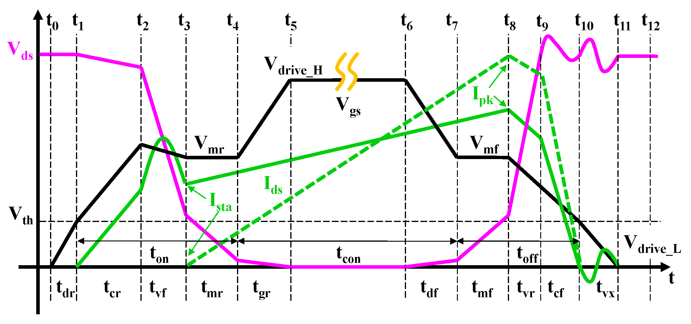
Figure 3.
The lumped simulation circuit with an extra parasitic capacitor.
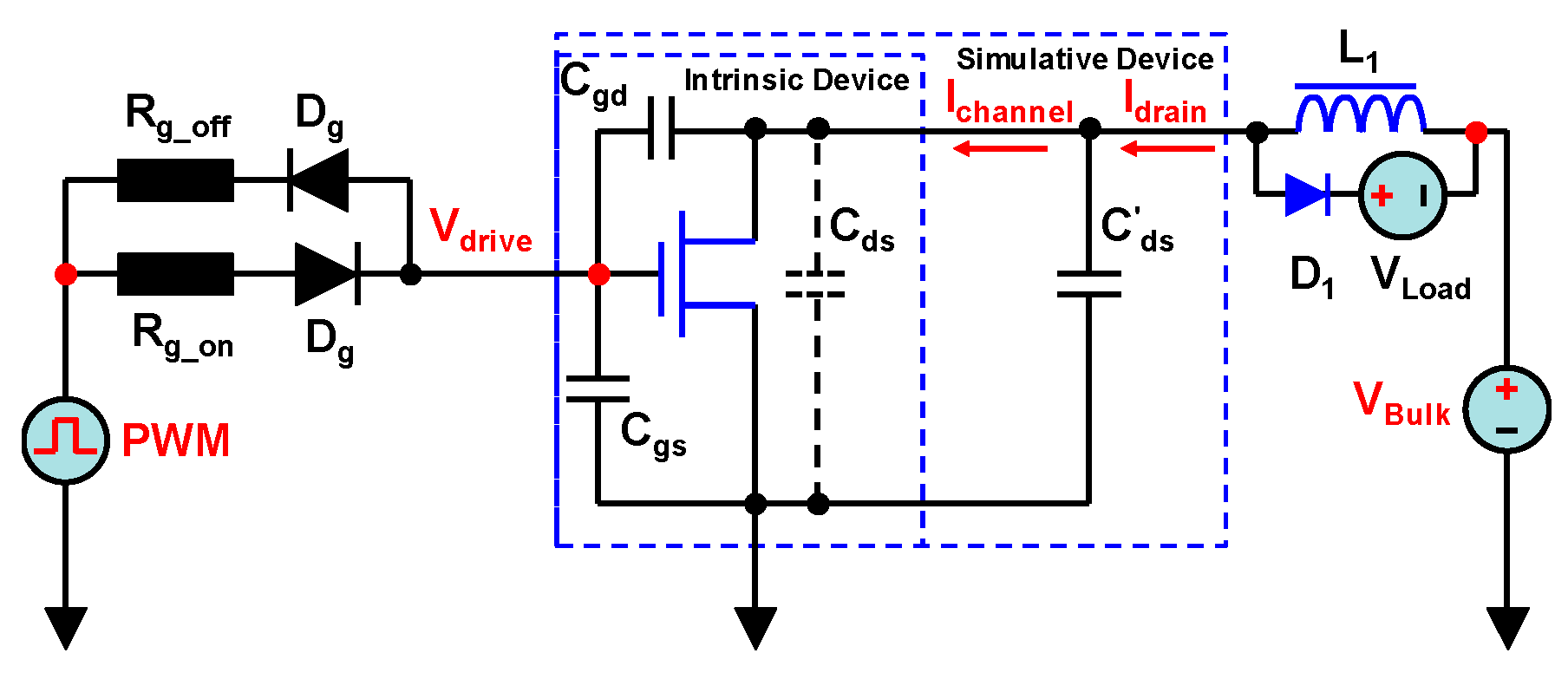
Figure 4.
Mechanism for the dynamic Rdson.
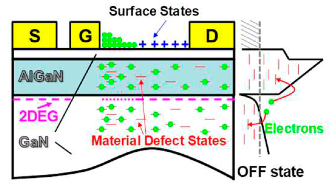
Figure 5.
Dynamic Rdson extraction waveforms at various fs (a) and the dynamic Rdson normalized by Rdson_DC for various Vds_off (b), fs (c), duty cycles (d), Idrain (e) and temperatures (f).
Figure 5.
Dynamic Rdson extraction waveforms at various fs (a) and the dynamic Rdson normalized by Rdson_DC for various Vds_off (b), fs (c), duty cycles (d), Idrain (e) and temperatures (f).
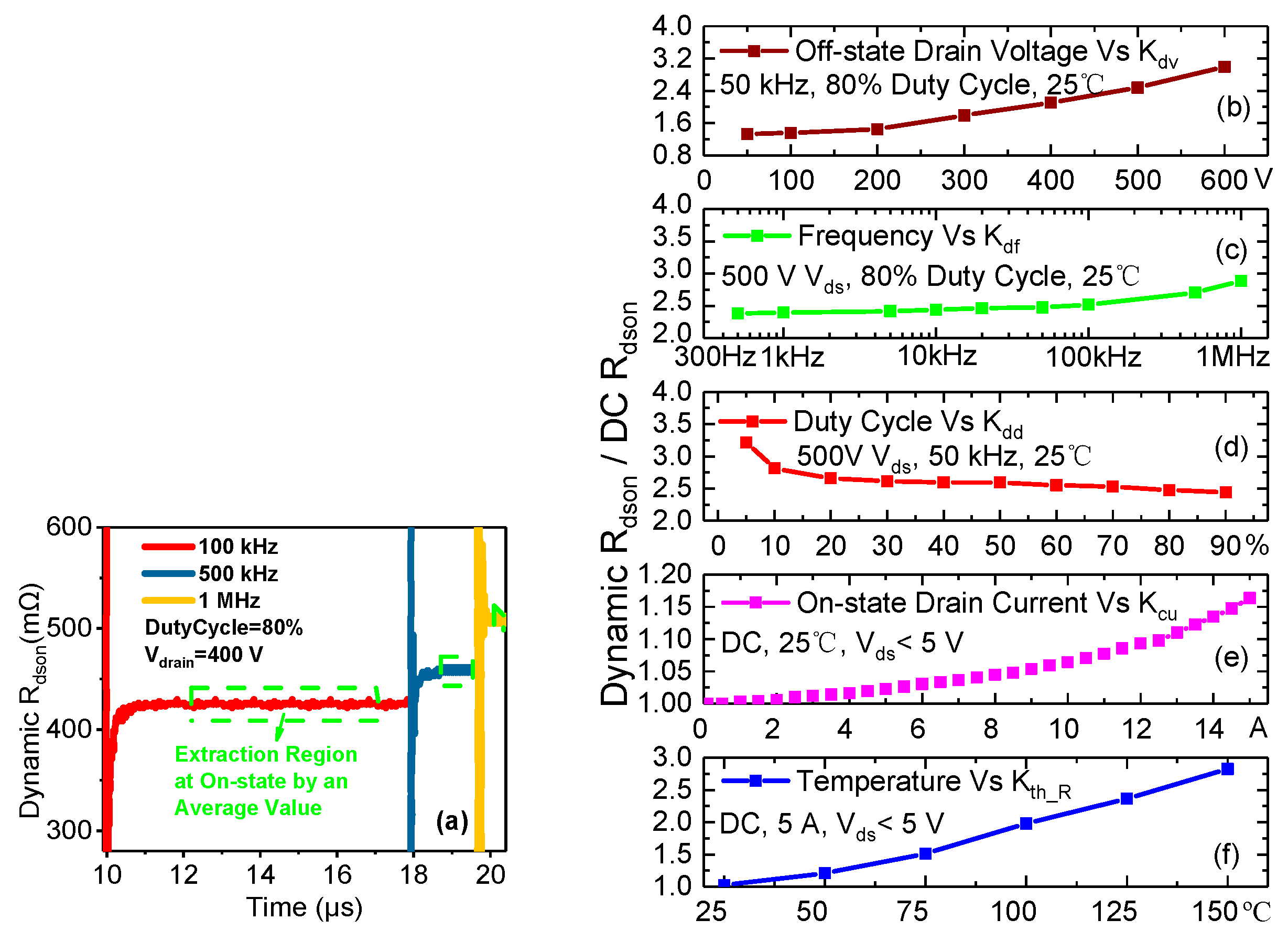
Figure 6.
Experimental waveforms of the HEMT device during the turn-on transitions in 400 V DCM with a VLoad of 80 V (a) and 400 V CCM with a VLoad of 20 V (b) and during turn-off transitions in 400 V DCM with a VLoad of 80 V (c) and 400 V CCM with a VLoad of 20 V (d).
Figure 6.
Experimental waveforms of the HEMT device during the turn-on transitions in 400 V DCM with a VLoad of 80 V (a) and 400 V CCM with a VLoad of 20 V (b) and during turn-off transitions in 400 V DCM with a VLoad of 80 V (c) and 400 V CCM with a VLoad of 20 V (d).
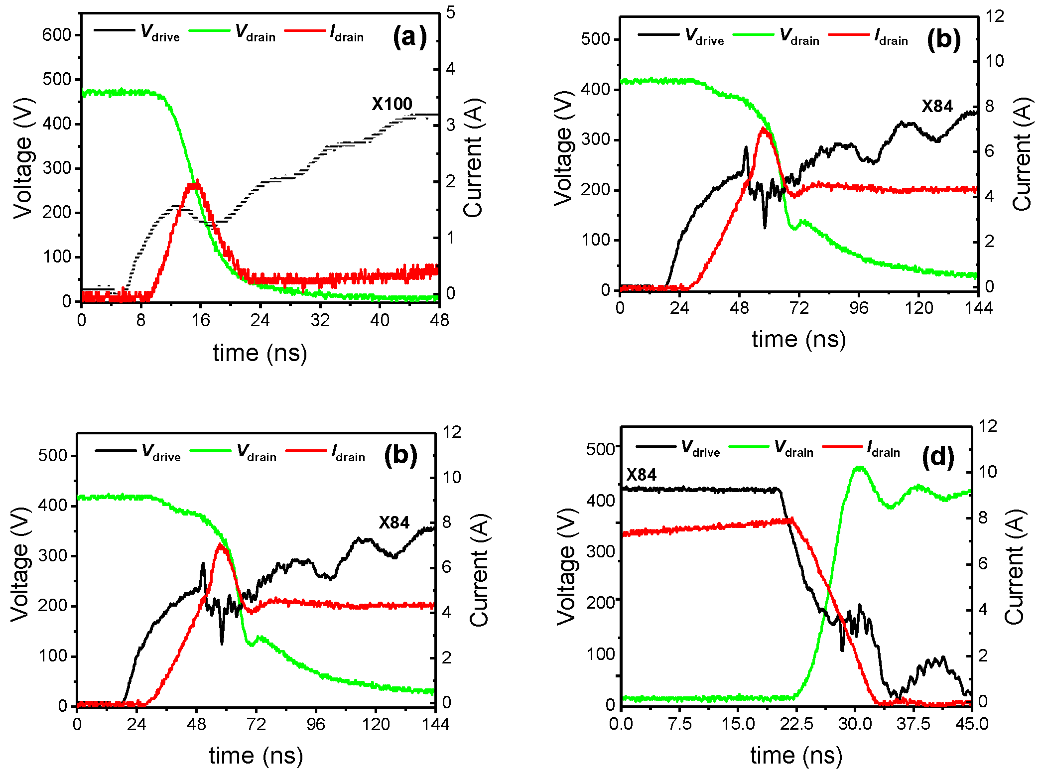
Figure 7.
Experimental results during the turn-on transition in 500 V CCM (a) and a schematic diagram of the corresponding current path (b) and the experimental results during the turn-off transition in 500 V CCM and a schematic diagram of corresponding current path (d).
Figure 7.
Experimental results during the turn-on transition in 500 V CCM (a) and a schematic diagram of the corresponding current path (b) and the experimental results during the turn-off transition in 500 V CCM and a schematic diagram of corresponding current path (d).
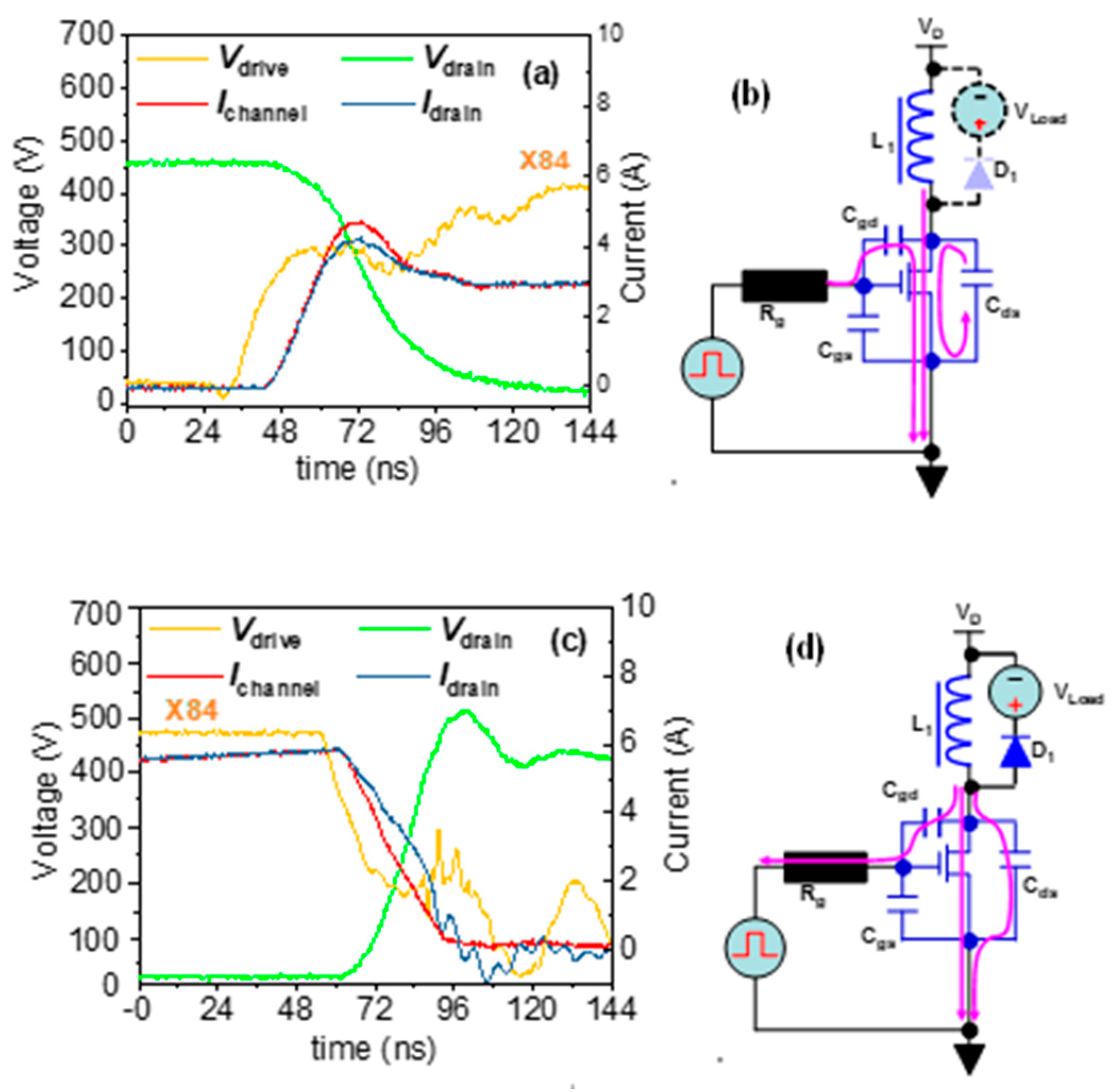
Figure 8.
Timing diagram of the GaN HEMT devices.
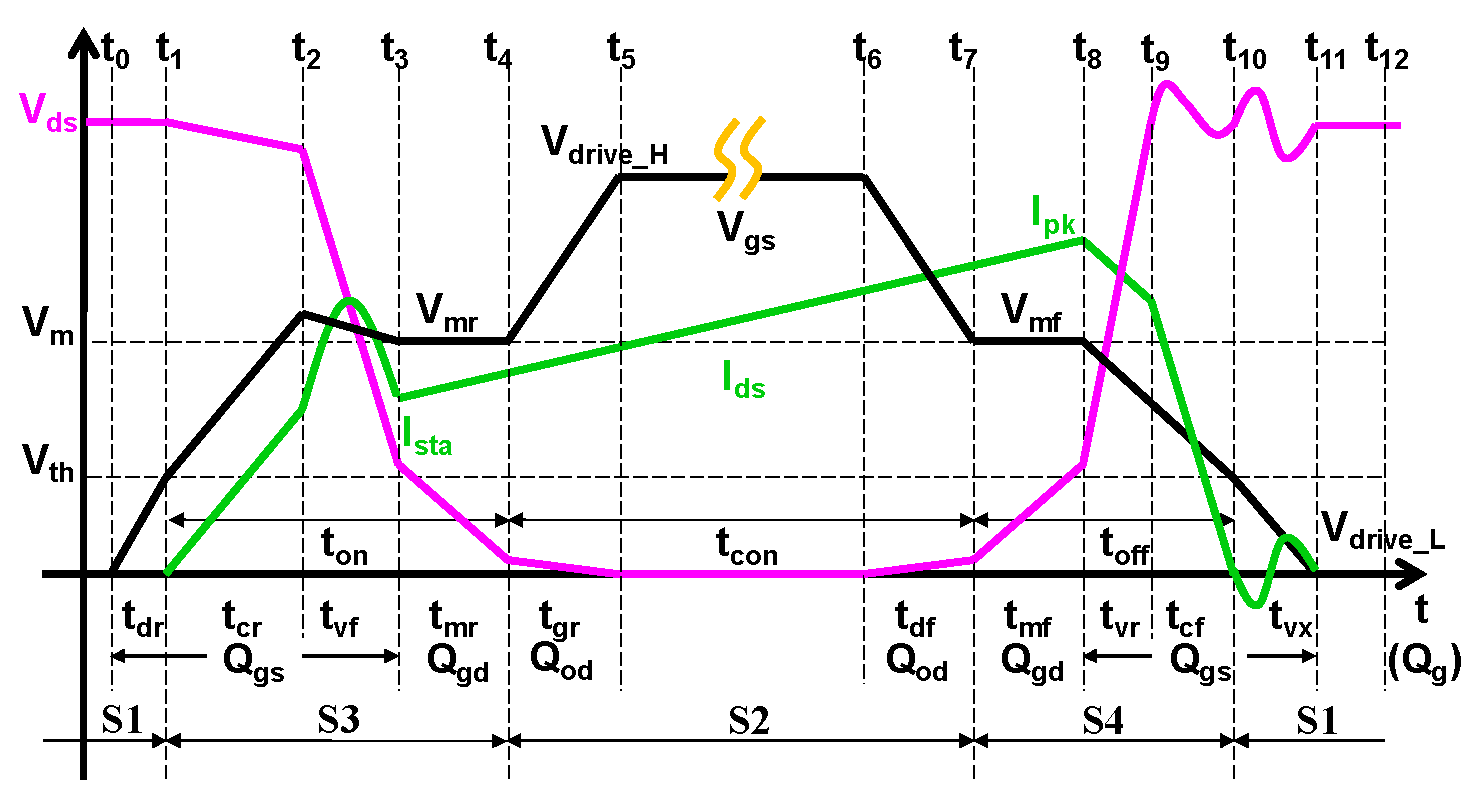
Figure 9.
The relationship between Io and Vo, Po, and Ipk (a) and the relationship between Io and inductance of L1 for various fs (b) in an open-loop controlled floating buck-boost power converter.
Figure 9.
The relationship between Io and Vo, Po, and Ipk (a) and the relationship between Io and inductance of L1 for various fs (b) in an open-loop controlled floating buck-boost power converter.

Figure 10.
Comparison of the total dynamic power losses from the analytical and experimental results both in CCM and DCMs and for various Io (a), fs (b) and VBulk (c).
Figure 10.
Comparison of the total dynamic power losses from the analytical and experimental results both in CCM and DCMs and for various Io (a), fs (b) and VBulk (c).
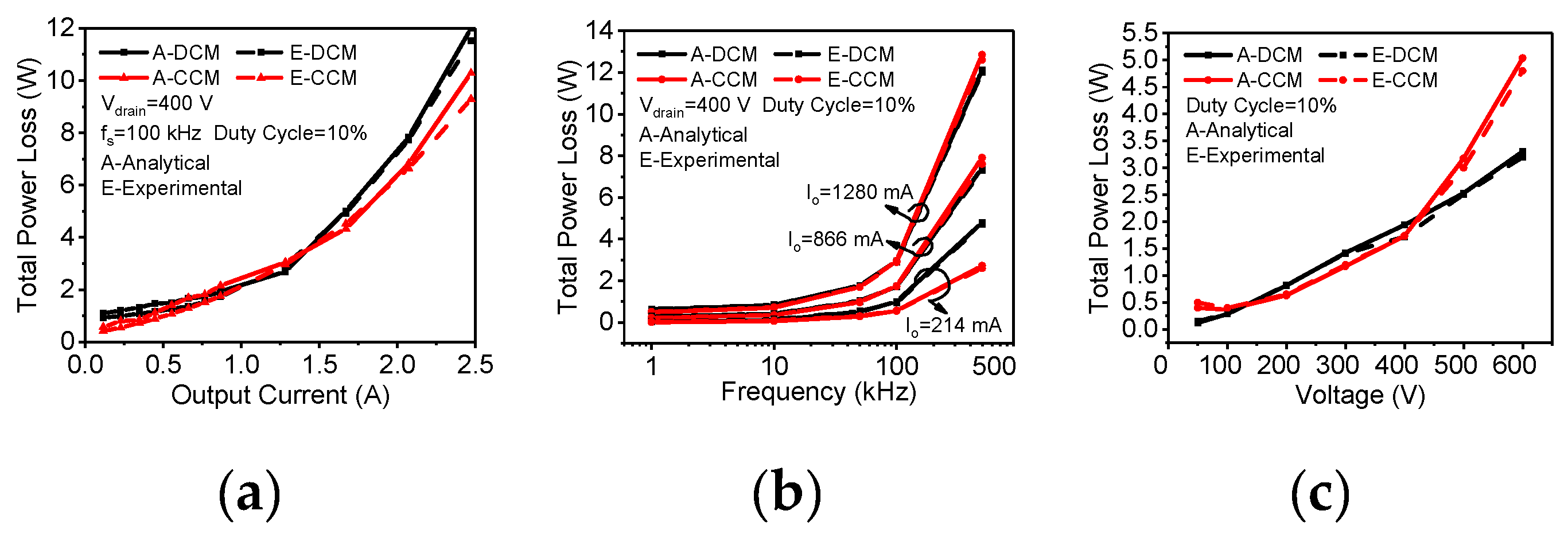
Figure 11.
Experimental total dynamic power losses (a) and switching losses (b) as a function of the output current in DCM and CCM
Figure 11.
Experimental total dynamic power losses (a) and switching losses (b) as a function of the output current in DCM and CCM
Disclaimer/Publisher’s Note: The statements, opinions and data contained in all publications are solely those of the individual author(s) and contributor(s) and not of MDPI and/or the editor(s). MDPI and/or the editor(s) disclaim responsibility for any injury to people or property resulting from any ideas, methods, instructions or products referred to in the content. |
© 2023 by the authors. Licensee MDPI, Basel, Switzerland. This article is an open access article distributed under the terms and conditions of the Creative Commons Attribution (CC BY) license (https://creativecommons.org/licenses/by/4.0/).
Copyright: This open access article is published under a Creative Commons CC BY 4.0 license, which permit the free download, distribution, and reuse, provided that the author and preprint are cited in any reuse.


