
Submitted:
21 October 2024
Posted:
21 October 2024
You are already at the latest version
Abstract
This study systematically investigates the effects of different anode work function metals (Ti/Au and Ni/Au) on the transport and temperature characteristics of β-Ga2O3 based Schottky barrier diodes (SBD), junction barrier Schottky diodes (JBSD), and P-N diodes (PND), utilizing Sentaurus TCAD simulation software for mechanistic analysis. From the perspective of transport characteristics, it is observed that the SBD exhibits a lower turn-on voltage and a higher current density. Notably, the turn-on voltage (Von) of the Ti/Au anode SBD is merely 0.2 V, marking the lowest recorded value in the existing literature. Furthermore, our study reveals that the turn-on voltages of the two types of PNDs are nearly identical, confirming that the contact between the anode metals and NiOx is ohmic contact, and the contact between Ni/Au and NiOx exhibits a lower contact resistance. The Von, current density, and variation rate of the JBSD lie between those of the SBD and PND. In terms of temperature characteristics, all diodes can work at 200 °C, with both current density and Von showing a decreasing trend as the temperature increases. Among them, the PND with a Ni/Au anode exhibits the best thermal stability, with reductions in Von and current density of 8.20% and 25.31%, respectively, while the SBD with a Ti/Au anode shows the poorest performance, with reductions of 98.56% and 30.97%. Finally, the reverse breakdown (BV) characteristics of all six devices are tested. The average BV for the PND with Ti/Au and Ni/Au anodes reach 1575 V and 1550 V, respectively. Moreover, although the Von of the JBSD decreases to 0.24 V, its average BV is approximately 220 V. This study demonstrates that β-Ga2O3 based power diodes continue to exhibit excellent characteristics and application prospects in terms of low turn-on voltage.
Keywords:
β-Ga2O3
; diode
; turn-on voltage
; temperature characteristic
; contact resistance
1. Introduction
β-Ga2O3 is a typical semiconductor material with a band gap of 4.9 eV and breakdown electric field of 8 MV/cm [1,2]. Owing to its excellent strength of high breakdown and low conduction loss [3], the potential application market in high-power electronic devices and circuits is inestimable. Besides, due to its better compatibility with traditional melt-grown methodology [4], the manufacturing cost is controllable compared to GaN and SiC. Therefore, the research on β-Ga2O3 materials and devices is of great significance.
At present, the research on β-Ga2O3 power diodes is still a hot topic, and how to increase breakdown voltage and reduce specific on-resistance are especially essential. Because they are useful to generate better power characteristics so as to achieve a higher Baliga’s figure-of-merit (BFOM) [5]. In fact, there are many ways to optimize the BFOM, such as field plates [6,7], trench [8], ion implantation [9], thermal oxidation [10], hetero-junction [11] and composite terminal structure [12,13,14,15]. And these methods have been verified to be effective. It is worth to point out that Li [14] et al propose the highest BFOM value of 13.2 GW/cm2, which combines thicker, lower drift layers and effective edge termination.
Although research on β-Ga2O3 power diodes remains focused on improving the BFOM value. In practical applications, the turn-on voltage (Von) of the device is also crucial, as it affects the conduction losses of the device. For β- Ga2O3, due to its smaller electron affinity of 3.15 eV [16], the theoretical barrier height is higher. Consequently, the turn-on voltage of β-Ga2O3 based diodes is usually around 0.9 V [17,18], which limits the potential application of β-Ga2O3 based diodes in switching power supplies. Therefore, it is necessary to conduct further research to lower Von. Therefore, it is necessary to conduct more research on the turn-on voltage. Several methods for reducing the turn-on voltage have been reported, such as trench structure [8], high-κ TiO2 interlayer [19], hydrogen treatment [20], N2O plasma treatment [21] and so on. In addition, low work function anode has been proven to be effective methods to decrease Von [22]. However, low work function anodes can lead to a decrease in breakdown voltage. Additionally, research on the thermal stability and conduction mechanisms of low work function anode diodes remains insufficient.
In this work, the effect of different anode metals on Von of Schottky barrier diodes (SBD) is studied by Sentaurus TCAD simulation. The definition of Von was consistent with the Ref. 21. It was confirmed that a smaller work function can effectively reduce the device's Von. Therefore, six types of device structures about SBDs, p-NiOx/β-Ga2O3 diodes (PNDs) and junction barrier Schottky diodes (JBSDs) are designed and the effects of two anode metals (Ti/Au and Ni/Au) on the forward conduction, temperature stability, and reverse breakdown characteristics are researched. Then the conclusions were drawn by specific comparative analysis.
2. Materials and Methods
For conventional diodes, different anode metals have different work functions. A smaller work function can effectively reduce the barrier for electron transitions, thereby inducing more electrons to transfer to the conduction band. Consequently, under the same applied voltage, diodes with lower work function anodes will turn on more easily, resulting in a larger current. Therefore, selecting an anode metal with a lower work function is beneficial for reducing the turn-on voltage of the diode. To further verify this, Sentaurus TCAD simulation software is used to design a basic diode, as shown in Figure 1(a). By selecting different anode metals and considering only the impact of work function on device performance [23], the corresponding turn-on voltage and current density are extracted and shown in Figure 1(b). The results indicate that when Ti is chosen as the anode metal, the device exhibits a minimum turn-on voltage of 0.3 V and a maximum current density of 850 A/cm². Based on these simulation results, β-Ga2O3 based SBD, PND, and JBSD diodes with Ti/Au anode metals are fabricated and tested. Meanwhile, similar devices with Ni/Au anodes are designed and fabricated for comparison.
The wafer consisted of a 10 μm thick Si doped β-Ga2O3 drift layer grown on a conductive (001) β-Ga2O3 substrate (Sn doping concentration of 2.0✕1018 cm-3). The net doping concentration (ND-NA) of the drift layer was determined to be 1.5×1016 cm-3. The fabrication processes started with ohmic contacts formed by an alloyed Ti/Au metal stack annealed at 470 °C for 1 min, and the wafer was cleaned by HF acid to remove surface impurities and oxides on the anode region, following washed with acetone, ethanol, water and finally dried. Then, the wafer was divided into six regions. For regions B and E, 40 nm p-NiOx layer was deposited on the whole anode region by Sputter in a mixed gas atmosphere of O2/Ar, and for regions C and F, the p-NiOx layer was selective deposited on the anode region with the same thickness. Then, each region needs to deposit metal (Ti/Au or Ni/Au) and lift off to form the anode. In regions A and D, the metal is contact with the drift layer directly, which could fabricate the Schottky diodes (SBDs). In regions B and E, the metal is contact with NiOx, which forms a PN junction with Ga2O3, thus enabling the fabrication of heterojunction PN diodes (PNDs) in these regions. For regions C and F, due to the selective deposition of NiOx, the metal contacts both NiOx and Ga2O3, which could fabricate the junction barrier diodes (JBSDs). The anode metals and diode structures for the six regions are listed in Table 1.
Circular device structures are set in all devices, and the radius of anode electrode is 50 μm. For JBSDs, the diameter of single NiOx is 4 µm and the spacing between adjacent NiOx is 5 µm. The structural diagrams and scanning electron microscope (SEM) images of these six devices are shown in Figure 2. The Agilent B1500 and B1505 semiconductor parameter analyzers were used for measurement.
3. Results and Discussion
The forward I-V characteristics of these samples are shown in Figure 3(a). The results indicate that the turn-on voltages of samples A and D are approximately 0.21 V and 0.81 V, respectively. This is because the work function of Ti is relatively low, at 4.33 eV, significantly reducing the barrier height between the metal and the β-Ga2O3 drift layer. The Von values for samples B and E are 2.08 V and 2.07 V, respectively. When the applied voltage of anode is below 6 V, the current curves for samples B and E almost coincide, indicating that Ti/Au and Ni/Au form the same type of metal-semiconductor contact with p-NiOx. Different Schottky metals form different barrier heights, resulting in variations in their current curves. This suggests that the metal/NiOx contact is an ohmic contact. Theoretically, the metal work functions (Wm) of Ti and Ni are 4.33 eV and 5.15 eV, respectively, while the work function of NiOx is approximately the algebraic sum of its electron affinity () and bandgap (Eg). The band diagrams of the metal and p-NiOx are shown in Figure 3(b), with the work function of p-NiOx calculated to be 5.5 eV. Due to the high doping concentration and large work function of p-NiOx, it is easier to achieve good ohmic contact. Additionally, PNDs have the highest Von, while SBDs have the lowest Von, indicating that the depletion effect of the heterojunction between p-NiOx and β-Ga2O3 is stronger than that of the Schottky junction between the anode metal and β-Ga2O3. For JBSDs, Von is determined by the smaller value between SBDs and PNDs, with the corresponding values for samples C and F being 0.24 V and 0.89 V, respectively. At the same forward voltage, the current density of JBSDs is slightly lower than that of SBDs due to the larger depletion region created by the p-NiOx/β-Ga2O3 heterojunction. Despite the metal/NiOx contact types of the two PNDs, the current density of sample E is slightly higher than that of sample B when the applied voltage of anode exceeds 6 V, possibly due to different contact resistances between the anode metals and p-NiOx. Relevant studies indicate that the contact resistance () between the metal and the p-type semiconductor is almost unaffected by temperature within the range of 200 ℃ [24].
Additionally, satisfies the constraint relationship:, where εs is the dielectric constant of p-NiOx, m∗is the effective mass of the carriers, is the barrier height, is the reduced Planck constant, and N is the carrier concentration of p-NiOx [25]. The only difference is that samples B and E have different between anode metal and p-NiOx, which can be calculated using the following formula: [26]. The results indicate that sample E has a lower , resulting in a smaller . As the applied voltage of anode gradually increases, the depletion region width will decrease. Therefore, the resistance of the PN junction will decrease, making the contact resistance between the anode metal and NiOx more prominent. Consequently, the current density of sample E is slightly higher than that of sample B. When the applied voltage of anode reaches 8 V, the corresponding current densities of samples B and E are 651 A/cm² and 665 A/cm², respectively.
The temperature-dependent I-V curves of these samples are shown in Figure 4. Figure 4(a) and Figure 4(b) present the I-V curves of the devices under linear and semi-logarithmic scales, respectively. Figure 4(c) and Figure 4(d) extract and provide the variation of current density (@ 8 V) and turn-on voltage (Von) with temperature increase for six samples. According to the thermionic emission (TE) theory [27,28], when the device current approaches saturation, the current density is negatively correlated with temperature. Clearly, all samples exhibit this characteristic. The results indicate that sample A has the highest current density, which is attributed to the presence of only a Schottky junction and a low work function metal. Due to the bandgap narrowing effect [29] and thermally-enhanced carrier diffusion [30], the Von of all samples decreases to varying degrees as the external temperature increases. The Von of the two PNDs is almost identical, but the current density at 8 V differs, consistent with previous results. Additionally, for the same anode metal, the turn-on voltage of JBSDs is slightly higher than that of SBDs. When the external temperature is set to 473 K, the Von of Samples A and C approaches zero.
Moreover, Table 2 presents the current density, turn-on voltage, and their respective change rates for the six samples at 300 K and 473 K. The results indicate that samples B and E exhibit relatively small change rates in both Von and current density. This suggests that the PND demonstrate better thermal stability, which is associated with the higher barrier height. Specifically, the larger work function of Ni increases the barrier for electron transfer from β-Ga2O3 to the anode metal, thereby maintaining better thermal stability over a wider temperature range (as described by thermal electron theory). Similarly, samples B and E have nearly identical Von values at 473 K. However, due to the poorer adaptability of Ti to high temperature environments, the thermal stability of sample B is slightly lower than that of sample E. In summary, when comparing the three types of devices, the PND exhibit superior thermal stability compared to the SBD, with the JBSD lying in between. Sample E shows the lowest change rate, while sample A has the highest, with change rates in current density of 25.31% and 30.97%, respectively. In terms of the variation in Von, samples A and C exhibit the largest change rates, indicating that the barrier height between Ti and Ga2O3 is the lowest, resulting in the poorest thermal stability.
The reverse breakdown characteristics of these samples are shown in Figure 5. In this letter, the corresponding reverse anode voltage when the anode current reaches 1 mA is defined as the breakdown voltage (BV). We tested three devices for each of the six samples, obtaining average breakdown voltages values of 145, 1575, 220, 370, 1550, and 895 V for the six samples, respectively. Due to the optimal reverse voltage withstand capability of the PN junction, samples B and E have the highest breakdown voltages [31]. Additionally, their BV values are almost identical, further indicating consistent contact between the anode metal and p-NiOx. Furthermore, the results show that the breakdown voltage of sample D is higher than that of sample A. This is because Ti has a smaller work function, reducing the barrier for carrier transition, thereby increasing the probability of electron tunneling in the off-state and resulting in higher reverse leakage current [32]. Moreover, it is found that the Von of sample C is approximately 0.24 V, while its breakdown voltage can reach 220 V without a field terminal structure. This indicates that β-Ga2O3 based diodes can achieve low power consumption and high breakdown voltage.
5. Conclusions
In conclusion, this work systematically investigates the effects of different anode work function metals (Ti/Au and Ni/Au) on the transport characteristics and temperature behavior of β-Ga2O3 based SBD, JBSD, and PND, utilizing Sentaurus TCAD simulation software for mechanistic analysis. To this end, six types of diodes with Ti/Au and Ni/Au have been designed and fabricated. Through testing and analysis, it is observed that the SBD exhibits a lower turn-on voltage and a higher current density. Notably, the Von of the Ti/Au anode SBD is merely 0.2 V, marking the lowest recorded value in the existing literature. Furthermore, our study reveals that the turn-on voltages of the two types of PNDs are nearly identical, confirming that the contact between the anode metals and NiOx is ohmic contact, and the contact between Ni/Au and NiOx exhibits a lower contact resistance. The Von, current density, and variation rate of the JBSD lie between those of the SBD and PND. In terms of temperature characteristics, all diodes can work at 200 °C, with both current density and Von showing a decreasing trend as the temperature increases. Among them, the PND with a Ni/Au anode exhibits the best thermal stability, with reductions in Von and current density of 8.20% and 25.31%, respectively, while the SBD with a Ti/Au anode shows the poorest performance, with reductions of 98.56% and 30.97%. Finally, the reverse breakdown (BV) characteristics of all six devices are tested. The average BV for the PND with Ti/Au and Ni/Au anodes reach 1575 V and 1550 V, respectively. Moreover, although the Von of the JBSD decreases to 0.24 V, its average BV is approximately 220 V. This indicates that β-Ga2O3 based diodes have broad application prospects in huge power circuits and equipment with advantages of low switch loss and high breakdown voltage.
Author Contributions
Conceptualization, Y.H. and B.S.; methodology, Y.H., X.L., G.C. and X.Z.; software, B.S. and P.L.; validation, Y.H., B.S., P.L., W.C., L.W., and J.Y.; formal analysis, Y.H., G.C. and X.Z.; investigation, B.S. and P.L.; resources, Y.H., X.L., G.C., X.Z., X.M. and Y.H.; data curation, Y.H. and B.S.; writing—original draft preparation, Y.H., B.S.; writing—review and editing, Y.H., P.L., Y.Z., X.W. and X.L.; visualization, B.S.; supervision, Y.H., X.L., X.Z., X.M. and Y.H.; project administration, Y.H.; funding acquisition, Y.H. All authors have read and agreed to the published version of the manuscript.
Funding
This work was supported by the National Natural Science Foundation of China under Grant Nos. 62474133 and U2241220, the opening project of state key laboratory of wide bandgap semiconductor devices and integrated technology under Grant No. 2413S111, the fundamental research funds for the central universities of China under Grant Nos. QTZX23019 and ZDRC2002.
Data Availability Statement
The original contributions presented in the study are included in the article/supplementary material, further inquiries can be directed to the corresponding author/s.
Conflicts of Interest
The authors declare no conflicts of interest.
References
- Stepanov, S.I.; Nikolaev, V.I. Gallium oxide: properties and applications - a review. Rev. Adv. Mater. Sci. 2016, 44, 63–86. [Google Scholar]
- Zhou, H.; Zhang, J.C. A review of the most recent progresses of state-of-art gallium oxide power devices. J. Semicond. 2019, 40, 011803. [Google Scholar] [CrossRef]
- Li, W.S.; Nomoto, K. Guiding principles for trench Schottky barrier diodes based on ultrawide bandgap semiconductors: a case study in Ga2O3. IEEE Trans. Electron Devices 2020, 67, 3938–3947. [Google Scholar] [CrossRef]
- Kuramata, A.; Koshi, K. High-quality β-Ga2O3 single crystals grown by edge-defined film-fed growth. Jpn. J. Appl. Phys. 2016, 55, 1202A2. [Google Scholar] [CrossRef]
- Xue, H.W.; He, Q.M. An overview of the ultrawide bandgap Ga2O3 semiconductor-based Schottky barrier diode for power electronics application. Nanoscale Res. Lett. 2018, 13, 290. [Google Scholar] [CrossRef]
- Konishi, K.; Goto, K. 1-kV vertical Ga2O3 field-plated Schottky barrier diodes. Appl. Phys. Lett. 2017, 110, 103506. [Google Scholar] [CrossRef]
- Allen, N.; Xiao, M. Vertical Ga2O3 Schottky barrier diodes with small-angle beveled field plates: a Baliga’s figure-of-merit of 0.6 GW/cm2. IEEE Electron Device Lett. 2019, 40, 1399–1402. [Google Scholar] [CrossRef]
- Sasaki, K.; Wakimoto, D. First demonstration of Ga2O3 trench MOS-type Schottky barrier diodes. IEEE Electron Device Lett. 2017, 38, 783–785. [Google Scholar] [CrossRef]
- Lin, C.-H.; Yuda, Y. Vertical Ga2O3 Schottky barrier diodes with guard ring formed by nitrogen-ion implantation. IEEE Electron Device Lett. 2019, 40, 1487–1490. [Google Scholar] [CrossRef]
- Wang, Y.G.; Lv, Y.J. High-voltage (-201) β-Ga2O3 vertical Schottky barrier diode with thermally-oxidized termination. IEEE Electron Device Lett. 2020, 41, 131–134. [Google Scholar] [CrossRef]
- Huang, Y.; Yang, W. NiO/β-Ga2O3 heterojunction diodes with ultra-low leakage current below 10-10 A and high thermostability. Chin. Phys. B 2023, 32, 098502. [Google Scholar] [CrossRef]
- Li, W.S.; Nomoto, K. Field-plated Ga2O3 trench Schottky barrier diodes with a BV2/Ron,sp of up to 0.95 GW/cm2. IEEE Electron Device Lett. 2020, 41, 107–110. [Google Scholar] [CrossRef]
- Yan, Q.L.; Gong, H.H. Low density of interface trap states and temperature dependence study of Ga2O3 Schottky barrier diode with p-NiOx termination. Appl. Phys. Lett. 2022, 120, 092106. [Google Scholar] [CrossRef]
- Li, J.-S.; Wan, H.-H. Ultra-wide bandgap semiconductor Ga2O3 power diodes. ESC J. Solid State Sci. Technol. 2024, 13, 035003. [Google Scholar] [CrossRef]
- Wu, F.H.; Wang, Y.G. Superior performance β-Ga2O3 junction barrier Schottky diodes implementing p-NiO heterojunction and beveled field plate for Hybrid Cockcroft-Walton voltage multiplier. IEEE Trans. Electron Devices 2023, 70, 1199–1205. [Google Scholar] [CrossRef]
- Liu, Z.; Liu, Y.Y. Energy-band alignments at ZnO/Ga2O3 and Ta2O5/Ga2O3 heterointerfaces by X-ray photoelectron spectroscopy and electron affinity rule. J. Appl. Phys. 2019, 126, 045707. [Google Scholar] [CrossRef]
- Chen, H.; Wang, H.Y. Vertical β-Ga2O3 Schottky barrier diodes with field plate assisted negative beveled termination and positive beveled termination. IEEE Electron Device Lett. 2023, 44, 21–24. [Google Scholar] [CrossRef]
- Hao, W.B.; Wu, F.H. Improved vertical β-Ga2O3 Schottky barrier diodes with conductivity-modulated p-NiO junction termination extension. IEEE Trans. Electron Devices 2023, 70, 2129–2134. [Google Scholar] [CrossRef]
- Hendricks, N.S.; Farzana, E. Vertical metal-dielectric-semiconductor diode on (001) β-Ga2O3 with high-κ TiO2 interlayer exhibiting reduced turn-on voltage and leakage current and improved breakdown. Appl. Phys. Express 2023, 16, 071002. [Google Scholar] [CrossRef]
- Yue, S.Z.; Zheng, X.F. Effect of hydrogen on electrical performance of Pt/Au β-Ga2O3 (001) Schottky barrier diodes. IEEE Trans. Electron Devices 2023, 70, 2403–2407. [Google Scholar] [CrossRef]
- He, Y.L.; Sheng, B.S. Research on the β-Ga2O3 Schottky barrier diodes with oxygen-containing plasma treatment. Appl. Phys. Lett. 2023, 122, 163503. [Google Scholar] [CrossRef]
- Su, C.X.; Zhou, H. Low turn-on voltage and 2.3 kV β-Ga2O3 heterojunction barrier Schottky diodes with Mo anode. Appl. Phys. Lett. 2024, 124, 173506. [Google Scholar] [CrossRef]
- Michaelson, H.B. The work function of the elements and its periodicity. J. Appl. Phys. 1997, 48, 4729–4733. [Google Scholar] [CrossRef]
- Lim, W.T.; Stafford, P.W. Ni/Au ohmic contacts to p-type Mg-doped CuCrO2 epitaxial layers. Appl. Phys. Lett. 2007, 90, 142101. [Google Scholar] [CrossRef]
- Li, Y.-L.; Schubert, E.F. Low-resistance ohmic contacts to p-type GaN. Appl. Phys. Lett. 2000, 76, 2728–2730. [Google Scholar] [CrossRef]
- Abdy, H.; Aletayeb, M. Investigation of metal-nickel oxide contacts used for perovskite solar cell. AIP Adv. 2019, 9, 015216. [Google Scholar] [CrossRef]
- Wang, L.; Nathan, M.I. High barrier height GaN Schottky diodes: Pt/GaN and Pd/GaN. Appl. Phys. Lett. 1996, 68, 1267–1269. [Google Scholar] [CrossRef]
- Li, A.; Feng, Q. Investigation of temperature dependent electrical characteristics on Au/Ni/β-Ga2O3 Schottky diodes. Superlattices Microstuct. 2018, 119, 212–217. [Google Scholar] [CrossRef]
- Camuso, G.; Napoli, E. Effect of bandgap narrowing on performance of modern power devices. IEEE Trans. Electron Devices 2013, 60, 4185–4190. [Google Scholar] [CrossRef]
- Gong, H.H.; Zhou, F. 1.37 kV/12 A NiO/β-Ga2O3 heterojunction diode with nanosecond reverse recovery and rugged surge-current capability. IEEE T. Power Electr. 2021, 36, 12213–12217. [Google Scholar] [CrossRef]
- Zhou, H.; Zeng, S.F. Comprehensive study and optimization of implementing p-NiO in β-Ga2O3 based diodes via TCAD simulation. Crystals 2021, 11, 1186. [Google Scholar] [CrossRef]
- Roccaforte, F.; Via, F.L. Dual metal SiC Schottky rectifiers with low power dissipation. Microelectron. Eng. 2003, 70, 524–528. [Google Scholar] [CrossRef]
Figure 1.
(a) Schematics of simulated diode prototype. (b) Turn-on voltage and current density curves of anode metal with different work functions.
Figure 1.
(a) Schematics of simulated diode prototype. (b) Turn-on voltage and current density curves of anode metal with different work functions.
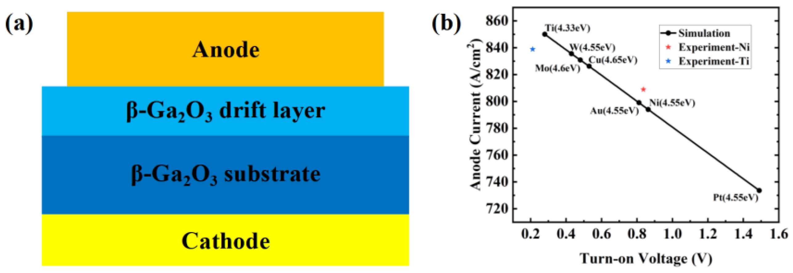
Figure 2.
(a) Schematics of samples A and D. (b) Schematics of samples B and E. (c) Schematics of samples C and F. (d) Cross-sectional SEM image of samples A and D. (e) Cross-sectional SEM image of samples B and E. (f) Cross-sectional SEM image of samples C and F.
Figure 2.
(a) Schematics of samples A and D. (b) Schematics of samples B and E. (c) Schematics of samples C and F. (d) Cross-sectional SEM image of samples A and D. (e) Cross-sectional SEM image of samples B and E. (f) Cross-sectional SEM image of samples C and F.
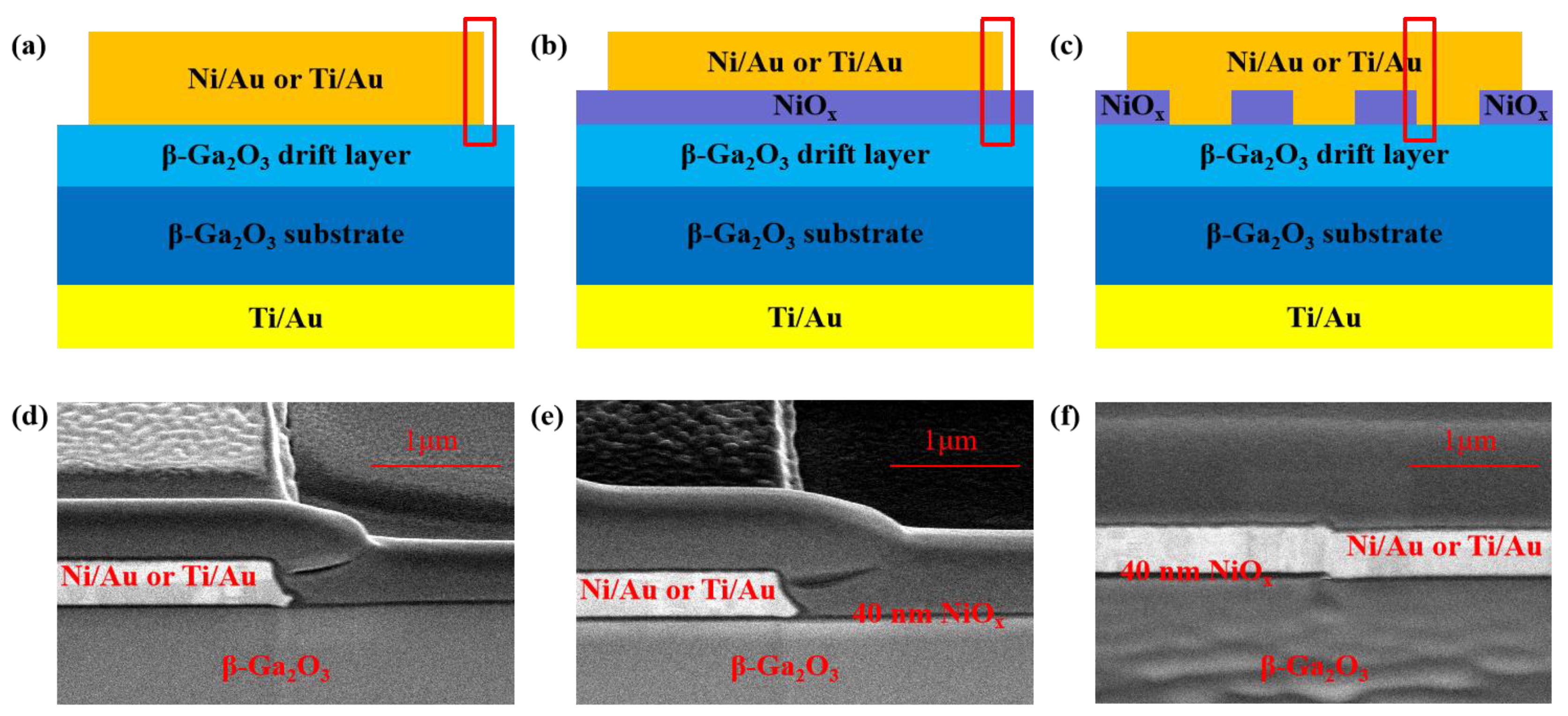
Figure 3.
(a) Forward I-V characteristics of six types of devices. (b) Schematic energy band diagram of metal and p-type NiOx.
Figure 3.
(a) Forward I-V characteristics of six types of devices. (b) Schematic energy band diagram of metal and p-type NiOx.
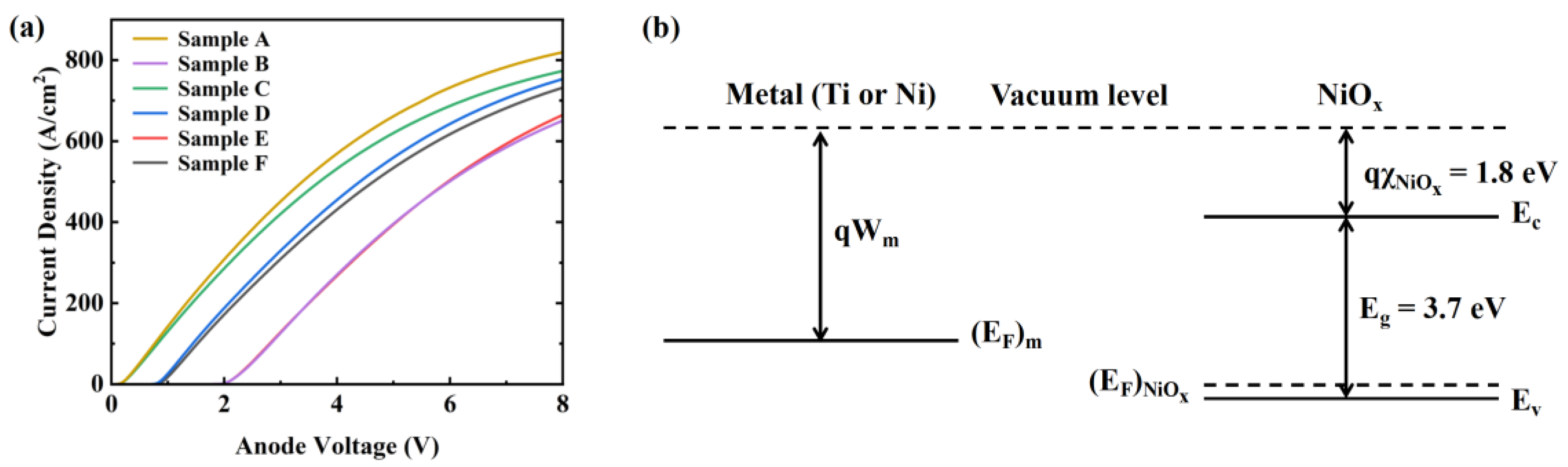
Figure 4.
(a) Temperature dependent IV characteristics of six types of devices in linear plot. (b) Temperature dependent IV characteristics of six types of devices in semi-logarithmic plot. (c) Current density curves of six types of devices. (d) Turn-on voltage curves of six types of devices.
Figure 4.
(a) Temperature dependent IV characteristics of six types of devices in linear plot. (b) Temperature dependent IV characteristics of six types of devices in semi-logarithmic plot. (c) Current density curves of six types of devices. (d) Turn-on voltage curves of six types of devices.
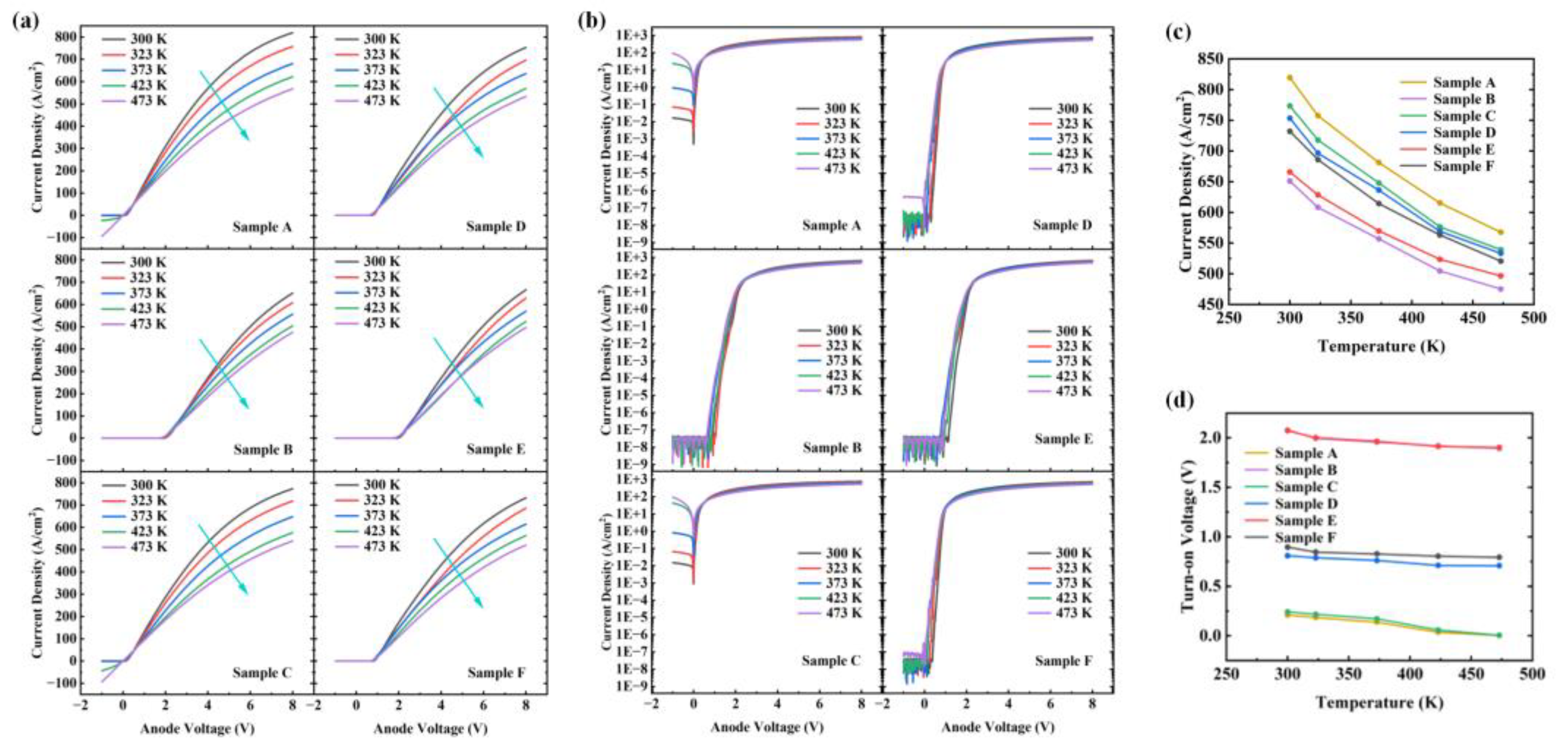
Figure 5.
The reverse breakdown characteristics of six types of devices.
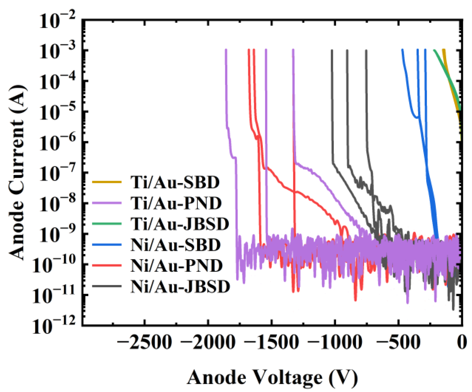

Table 1.
The structures and anode metals of six samples.
| Samples | A | B | C | D | E | F |
|---|---|---|---|---|---|---|
| Structure | SBD | PND | JBSD | SBD | PND | JBSD |
| Anode metal | Ti/Au | Ti/Au | Ti/Au | Ni/Au | Ni/Au | Ni/Au |
Table 2.
The data of current density and turn-on voltage at 300 K and 473 K.
| Samples | A | B | C | D | E | F |
|---|---|---|---|---|---|---|
| Von at 300 K (V) | 0.209 | 2.072 | 0.242 | 0.809 | 2.072 | 0.895 |
| Von at 473 K (V) | 0.003 | 1.901 | 0.005 | 0.708 | 1.902 | 0.793 |
| Variation value of Von (V) | 0.206 | 0.171 | 0.237 | 0.101 | 0.170 | 0.102 |
| Variation rate of Von | 98.56% | 8.25% | 97.93% | 12.48% | 8.20% | 11.40% |
| Current density at 300 K (A/cm2) | 807.4 | 651.0 | 770.9 | 753.4 | 664.9 | 732.1 |
| Current density at 473 K (A/cm2) | 565.6 | 475.2 | 541.6 | 533.3 | 496.6 | 520.5 |
| Variation value of current density (A/cm2) | 242.8 | 175.8 | 229.3 | 220.1 | 168.3 | 211.6 |
| Variation rate of current density | 30.97% | 27.00% | 30.29% | 29.21% | 25.31% | 28.90% |
Disclaimer/Publisher’s Note: The statements, opinions and data contained in all publications are solely those of the individual author(s) and contributor(s) and not of MDPI and/or the editor(s). MDPI and/or the editor(s) disclaim responsibility for any injury to people or property resulting from any ideas, methods, instructions or products referred to in the content. |
© 2024 by the authors. Licensee MDPI, Basel, Switzerland. This article is an open access article distributed under the terms and conditions of the Creative Commons Attribution (CC BY) license (http://creativecommons.org/licenses/by/4.0/).
Copyright: This open access article is published under a Creative Commons CC BY 4.0 license, which permit the free download, distribution, and reuse, provided that the author and preprint are cited in any reuse.


