
Submitted:
18 April 2023
Posted:
19 April 2023
You are already at the latest version
Abstract
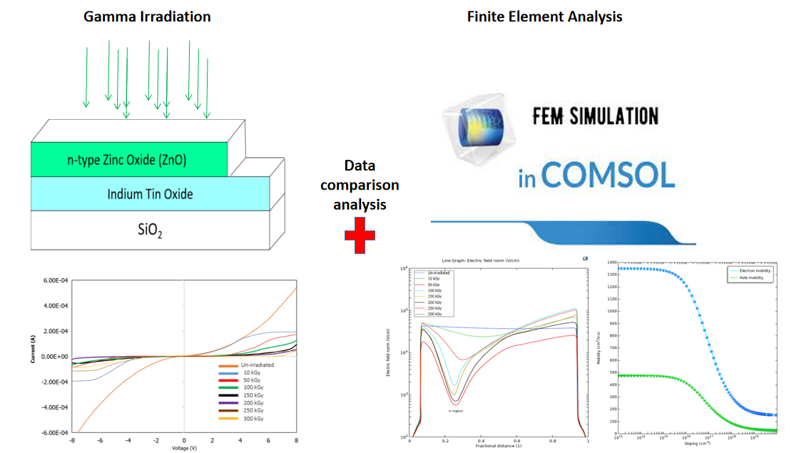
In this paper, we present the investigation results of radiation-induced effects in metal-oxide-semiconductor (MOS) doped with moderate amounts of Zinc Oxide (ZnO) as a potential candidate for space-borne application. The samples were fabricated via the sputtering method at a working pressure of 3mTorr and a deposition temperature of 300oC. The ZnO samples were exposed to 1.25-MeV gamma-ray utilizing Co60 source, and their electronic response was measured at ionizing doses ranging from 10 kGy to 300 kGy. A comparative work was performed through finite element method to simulate the electronic response of the PN junction diode due to ionizing radiation. The results indicate that the ideality factor of the MOS diode increases as the ionizing dose increases, rendering it unsuitable for use as a diode. The degradation of the electrical parameters was also simulated, showing the increase in hole concentration. These findings suggest that the ejection of electrons occurred, which agrees with the gamma radiation effects trend. Furthermore, as the intensity of radiation increases, the spatial charge that arises from the separation of hole-electron pairs results in a substantial reduction of the electric field in the central portion of the n-type region. These findings provide insights into the degradation of electrical parameters in MOS devices under gamma radiation and have implications for their use in space-borne applications.
Keywords:
MOS semiconductor
; Zinc Oxide
; Radiation Simulation
; Finite Element Analysis
; Radiation damage
; Space application
1. Introduction
There has been a growing trend of interest in metal oxide-based semiconductors (MOS) in recent times due to their superiority over silicon-based materials, as seen in recent studies [1,2,3,4]. This investigation focuses on Zinc Oxide (ZnO) as a potential semiconductor material that can endure intense radiation. ZnO possesses a wide bandgap of 3.34 eV at room temperature and a binding energy in the UV-A region (320-400 nm), along with attractive attributes such as a large surface area, low toxicity, chemical stability, electrochemical activity, and excellent conductivity [1,2,3]. Furthermore, CuGaO2 and Cu2O have the potential to form heterojunctions with ZnO-based semiconductors because of their low lattice mismatch [2]. Previous studies have revealed that ZnO films exposed to radiation from Cobalt-60 (Co-60) showed a decline in turn-on voltage and low-frequency noise [4,5], but an increase in electron mobility. These changes in electrical properties were attributed to the creation of interface states and electron-hole pairs in the insulating layer [5,6]. Research on ZnO's ability to withstand radiation is of utmost importance, as it has been discovered to be more resilient to radiation effects than conventional and emerging transistor technologies [1,2,3]. According to Nastasi et al. [7], bombardment with heavy ions possessing keV to MeV energy levels leads to lattice disorder that is influenced by ion species, energy, temperature, dose, and channeling effects. The formation of radiation damage is also dependent on ion mass, species, target temperature, dose, energy, and flux [8,9]. Bombardment with ions can alter physical, mechanical, electrical, optical, and magnetic properties, thus altering their overall properties [8]. Chee et al. [8] carried out a simulation of GaAs exposed to ion incident energy ranging from 100 keV to 3 MeV using stopping range in ion matter (SRIM) and discovered that high-energy photon exposure degrades electrical parameters due to displacement damage. Movla et al. [10] performed a similar study. The pre-irradiation work required before conducting irradiation experiments is a laborious process, hence a more efficient method is needed to simulate the impact of radiation on MOS semiconductors. This paper presents a proposal to simulate radiation damage trends using the finite element method and compares the results with physical experiment data.
2. Experimental Setup
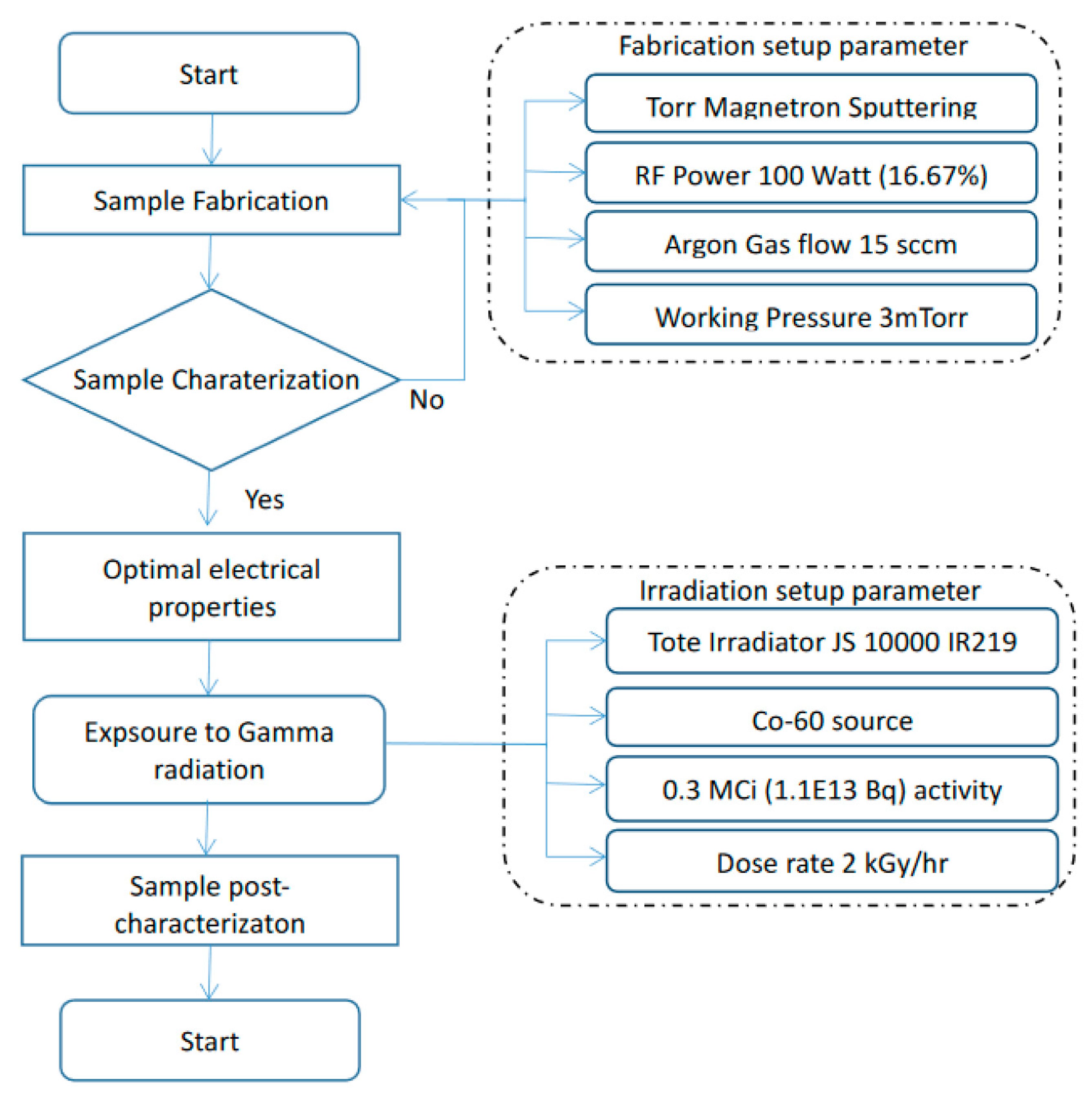
Initially, it was necessary to prepare and fabricate a physical sample to serve as a basis for the analysis of simulated data. This was accomplished through the utilization of a sputtering system for the deposition process. Subsequently, the samples were exposed to gamma radiation exposure from a Co-60 source. The irradiation was carried out using the JS10000 IR219 tote irradiator system by (MINTec-Sinagama) which boasts a high Co-60 radioactive activity [11,12,13,14] of approximately 0.3 MCi (1.1 x 10¹³ Bq) as per the Nuclear Agency of Malaysia [15]. The system had a dose rate of 2 kGy/hr and the films were exposed to a total ionizing dose ranging from 10 kGy to 300 kGy respectively.
Figure 1.
Flowchart on the irradiation setup.
2.1. Mathematical approach on the extraction of Schottky diode parameters.
Under normal circumstances, current flow in a diode is expressed as a function of diode voltage [16]:
The prefactor is represented by "", and the ideality factor, represented by "", is a factor included in the current-voltage (I-V) relationship to account for non-ideal behavior in diodes. The value of "n" typically falls between 1.5 and 2, and can vary among different semiconductor materials. If both the reverse saturation current, "Io", and the ideality factor, "n", remain constant within a certain current range, the relationship between log(I) and voltage will form a straight line. However, when series resistance starts to impact the diode's behavior, the voltage across the entire heterojunction diode, including substrate and contact resistance, and other series components, is represented by = V – Irs, and the current-voltage expression becomes [16,17]:
The equation for the Is is as follows
The effective area of the fabricated heterojunction diode is represented by "A", and "A*" represents the Richardson constant and the""Schottky barrier height of the diode. The series resistance, "RS", and the ideality factor, "n", are crucial parameters that indicate the electrical characteristics of the diodes. These values can be determined using the equation [2,16,17]:
2.2. Finite element analysis Governing equation
The electrical behavior of a semiconductor device is estimated hypothetically by applying equations that describe the flow of charge within the device while considering the limitations imposed by the diode's physical structure and electrical contacts. This approach provides insight into the distribution of electrons and holes and the strength of the electric field within the device. The obtained data is then incorporated into a finite element calculation to determine the final voltage and current levels over a period of time.
2.2.1. Carrier Transport Mathematical Equation
The calculation of the distribution and movement of carriers in a one-dimensional semiconductor device structure is achieved by resolving three fundamental equations [18].
The equation of continuity for holes,
The equation of continuity for electrons,
Poisson’s equation
Poisson’s equation connects the electric field and potential generated by the excess charge within a crystal with the charge itself. The equation involves the electric field strength I, the electronic charge (q) in the crystal, the Boltzmann constant (k), the permittivity of free space, the fundamental unit of charge (q), the concentrations of holes (p) and electrons (n), the concentrations of ionized donors (ND) and acceptors (NA), and the material’s permittivity (a intrinsic property that quantifies the opposition to the establishment of an electric field).
while
Equations (7) to (9) are subjected to boundary restrictions by incorporating appropriate boundary conditions. The applied voltage is represented by obtaining the integral of E(x, t) between two contacts to be equal to the specified voltage. Additionally, it is assumed that the electric field at both end contacts is null. The initial values for the hole and electron densities can either be specified by the analyst or obtained from the zero bias solution when the device is at rest.
and
In general, the functions gp, gn, ,µp, and µn vary at each point in the device according to the value of n, p, and E at that point.
2.2.2. Carrier Generation-Recombination Mathematical Equation
The terms responsible for producing carriers, gn and gp, consist of three main components: the formation and recombination of electrons and holes via imperfections, impact or avalanche ionization, and generation from ionizing radiation. The creation and recombination of holes and electrons through defects can be described using two varieties of the Shockley-Read-Hall (SRH) model: single-level models [17], which depict defects with neutral and solitary charge states, and multi-level models, which allow for the depiction of donor, acceptor, and neutral charge states. The rate at which holes and electrons are extracted from the valence and conduction bands by a single level center is represented by two equations that denote the formation-recombination rates[17].
In addition, a third equation describes the net rate of electron charge accumulation at the center.
If the center is an acceptor (i.e. it is capable of capturing electrons and becoming negatively charged), the charge density qNt- is included in Poisson's equation to take into account the trapped carriers' space charge. On the other hand, if the center is a donor, then the net positive charge q(Nt - N–-) is included in equation (3). The equations for the two-level model are similarly expressed [18].
The net trapped charge q(Nt - Nt-) is utilized in Poisson's equation. However, carrier generation through impact ionization (gnI and gpI) or ionizing radiation (gnR and gpR) differs from generation through a defect level in that it creates holes and electrons at equal rates. In the case of generation by ionizing radiation, the generation rates in ZnO are tied to the absorbed energy through a relationship [18].
The production of carriers through impact ionization is significantly influenced by the strength of the electric field and the quantity of holes and electrons in the area. This mechanism can be mathematically represented through the following equation [18].
Where and are given by the relations
2.2.3. Mobility Expressions
The traditional method adopted in many analytical studies assumes that the mobility of both electrons and holes remains constant [18]. However, in the case of devices experiencing large electric fields or variations in doping, it becomes imperative to consider the effect of these factors on the mobility. In the absence of high electric fields or ionized impurities, the mobility of carriers is primarily limited by lattice scattering[18]. However, when there is a substantial concentration of ionized impurities, the Coulomb potential generated by these impurities leads to scattering of electrons and holes, resulting in a decline of mobility with increasing impurity density[18,19]. Furthermore, the mobility of both electrons and holes is also impacted by the strength of the electric field [18]. When electric fields are high, carriers can accumulate sufficient energy between scatterings to raise their average energy or temperature, leading to frequent interactions with the lattice and a decrease in mobility. The limiting velocity of the carrier drift is depicted in Figure 2. The graph in Figure 2 exhibits experimental data on mobility, which can be represented by the following equations with a reasonable degree of accuracy[18].
The solid curves in Figure 2 represent the expressions that provide a reasonable approximation of the experimental data.
3. I–V characteristics curve of ZnO irradiated with gamma
The results depicted in Figure 3 reveal that the onset voltage of the hetero-diode in the manufactured sample experiences a substantial increase at 1.5V. As the exposure to growing doses of Total Ionizing Dose (TID) increases, the turn-on voltage also increases correspondingly. Once the dose reaches 50 kGy and higher, a noticeable alteration in the current region can be seen. Table 1 displays the ideality factor and series resistance of the diode for samples that were both un-irradiated and exposed to doses of 10 kGy- 300 kGy. With the increase in TID, the ideality factor of the n-ZnO/p-CuGaO2 diode tends to rise to a higher value, which implies that the diode is no longer ideal. This escalation is due to the presence of a considerable amount of dopants and impurities. The rise in ionizing radiation results in the degradation of the semiconductor diode, causing the series resistance, RS, to rise due to the decrease in the barrier height ɸ, as highlighted in Table 1.
3.1. Simulation Findings
The application of the Mathematical formulations and computational solution strategies outlined earlier in this text has employed the finite element method to examine the Charging and shifting impacts in junction devices constructed from semiconductors. The behavior of a reverse-biased PN diode exposed to both consistent and momentary ionizing radiation has been the subject of investigation by several researchers. However, prior studies have been limited to low levels of ionization and have only been able to obtain analytical solutions in closed form due to the limitations imposed by the assumptions made. The present analysis overcomes this limitation, yielding both consistent and momentary ionizing radiation for the general one-dimensional case without any assumptions. Figure 3 displays the doping profile simulated for this analysis.
Figure 3.
Impurity Doping Profile for PN diode.
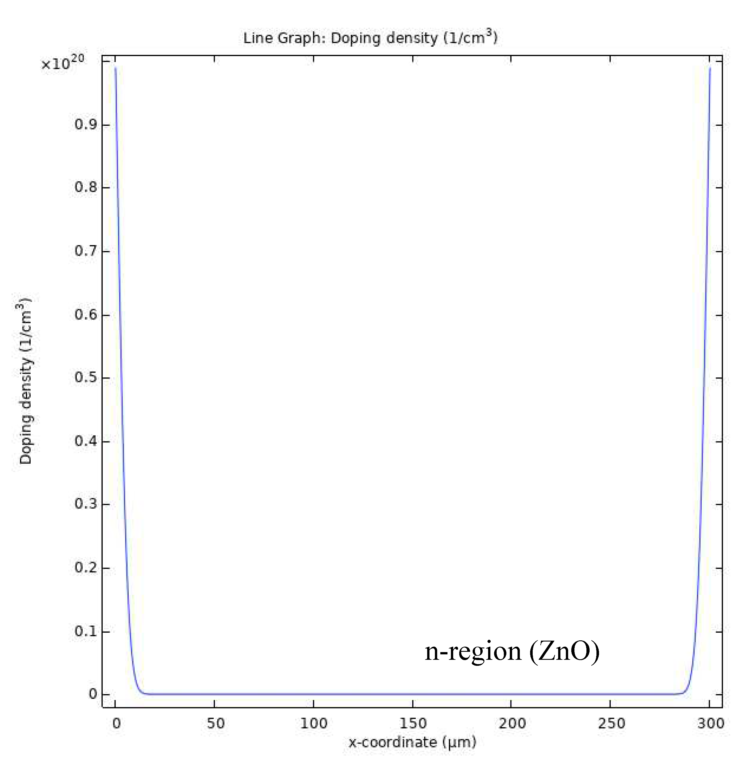
The hetero-diode (n-ZnO, p-CuGaO2) is made up of regions with high levels of impurities, referred to as N+ and P+. These regions are located within a 300nm wafer of essentially pure ZnO, resulting in a rapid transit time shorter than typical carrier lifetimes and causing minimal recombination. To increase the hole lifetime in the nth region, gold centers with a concentration of 1013/cm3 were introduced, but the effect of trapping was not considered. When the PN diode is put into reverse-bias, a depletion zone arises at the N+ junction and extends into the pi region. To understand this, Poisson's equation (2) and the continuity equations (3) can be solved to determine how the electric field and hole density vary with position and applied voltage.
3.1.1. Steady state analysis
In an ionization field with a low and steady state, the electrons and holes produced by radiation are promptly moved across the n-region due to the strong electric field. This results in a low concentration of free carriers, preventing the space charge produced by these carriers from significantly affecting the intensity of the field. However, when the intensity of the radiation is elevated, the separation of the electron-hole pairs results in a substantial increase in space charge, leading to a significant reduction of the field intensity within the n-type region.
The static electric field and hole distributions shown in Figure 4 exhibit the impact of energy infusion on the system at varying doses from 10 kGy to 300 kGy. A minor dose of 10 kGy already causes a noticeable shift in the electric field distribution, which intensifies significantly with a dose of 50 kGy as the central part of the region experiences a sharp decline. As the central field intensity decreases, a compensating rise can be observed at both edges of the n-type area. This alteration in the distribution of the electric field results in a rapid movement of holes from the left part of the n-type area into the area with low electric field, where the velocity of drift is greatly reduced.
As a result of the generation of carriers, the hole densities in the central region of the -type region significantly surpass the values observed in other areas of the same region. This phenomenon, which is easily discernible from the comparison between the curves representing 50 kGy and 100 kGy in Fig. 4b, exhibits a rapid escalation (from 1012 to 1016 /cm3) until the density of carriers in the center of the device becomes so considerable that recombination becomes a significant factor, resulting in a decrease in the collection efficiency of the diode. The swift increase in carrier density with dose rate leads to the conclusion that energy deposition rates of the magnitude of 50 kGy would likely cause a substantial reduction in the collection efficiency of the diode. The IV analysis, as indicated in Table 1, suggests a noteworthy enhancement in the ideality factor, which can be attributed to the decline in the collection efficiency of the diode and the concomitant increase in series resistance, which would result in a drastic reduction in electrical properties.
When subjected to gamma rays, the interaction with materials leads to the inevitable generation of defects, brought about by the ionizing properties of the rays and resulting in the ejection of electrons [20,21]. Additionally, atomic displacement, which results from irradiation and produces primary knock-on atoms (PKA), leads to lattice defects [22,23,24]. Studies have shown that exposure of ZnO-based semiconductors to gamma radiation results in a deterioration of their electrical parameters, as evidenced by a decrease in turn-on voltage, which is caused by structural defects present in the semiconductor, leading to an increase in its ideality factor [1,2,24,25]. These alterations can also be attributed to the combined effects of the creation of interface states and the generation of electron-hole pairs in the insulating layer. The simulated data clearly demonstrates an increase in hole concentration with increased dose, thereby confirming the ejection of electrons as the device interacts with ionizing radiation.
Conclusion
The impact of Total Ionizing Dose (TID) on materials can vary significantly. In this research, the effect of TID on a proposed diode through finite element analysis is simulated. The results indicate a decrease in the diode's efficiency as TID increases, with observable degradation in its electrical properties. Specifically, we noticed an increase in turn-on voltage from 1.5V to 7.3V and an increase in ideality factor from 2.8 to 102.16, indicating the presence of imperfections. This degradation is due to the ionizing properties of gamma rays. Our finite element simulation also showed an increase in hole concentration from 1012 to 1016/cm3, indicating electron vacancies caused by gamma radiation. As the intensity of radiation increased, the space charge created by separated hole-electron pairs reduced the field within the p-type region.
Acknowledgments
This work was supported by Ministry of Higher Education Fundamental Research Grant Scheme (FRGS) Year 2020, FRGS/1/2020/STG07/UMS/02/1 titled “Explication on the Damage Mechanism Induced by High Energy Radiation On ZnO based Photoconductive Radiation Detector for Space Borne Application”.
References
- Duinong, M., Rasmidi, R., Chee, F. P., Moh, P. Y., Salleh, S., Mohd Salleh, K. A., & Ibrahim, S. (2022). Effect of Gamma Radiation on Structural and Optical Properties of ZnO and Mg-Doped ZnO Films Paired with Monte Carlo Simulation. Coatings, 12(10), 1590. [CrossRef]
- Mivolil, D. S., Chee, F. P., Rasmidi, R., Alias, A., Salleh, S., & Salleh, K. A. M. (2020). Gamma ray and neutron radiation effects on the electrical and structural properties of n-ZnO/p-CuGaO2 Schottky diode. ECS Journal of Solid State Science and Technology, 9(4), 045019. [CrossRef]
- Chee, F. P., Duinong, M. I. V. O. L. I. L., Rani, A. I. A., Chang, J. H. W., Alias, A. F. I. S. H. A. H., & Salleh, S. A. A. F. I. E. (2019). Simulation of displacement damage cross section of cuprous oxide/zinc oxide (Cu2O/ZnO) based heterojunction device. J. Eng. Sci. Technol, 14(4), 1820-1834.
- Liu, Y.; Wu, W.-J.; En, Y.-F.; Wang, L.; Lei, Z.-F.; and Wang, X.-H. (2014). Total dose ionizing radiation effects in the indium-zinc oxide thin-film transistors. IEEE Electron Device Letters, 35(3), 369-371. [CrossRef]
- Indluru, A.; Holbert, K.E.; and Alford, T.L. (2013). Gamma radiation effects on indium-zinc oxide thin-film transistors. Thin Solid Films, 539, 342-344. [CrossRef]
- Lee, E. H., Indluru, A., Allee, D. R., Clark, L. T., Holbert, K. E., & Alford, T. L. (2011). Effects of gamma irradiation and electrical stress on a-Si: H thin-film transistors for flexible electronics and displays. Journal of Display Technology, 7(6), 325-329. [CrossRef]
- Nastasi, M.; Mayer, J.W.; and Hirvonen, J.K. (1996). Ion-solid interactions: fundamentals and applications. Cambridge, United Kingdom: Cambridge University Press.
- Chee, F.P.; Amir, H.F.A.; and Salleh, S. (2011). Range distribution and electronic stopping power for Cobalt (Co) ions in Gallium Arsenide (GaAs) optoelectronic devices. Proceedings of the 4 th International Conference on Modeling, Simulation and Applied Optimization (ICMSAO). Kuala Lumpur, Malaysia, 1-5. [CrossRef]
- Wendler, E. (2009). Mechanisms of damage formation in semiconductors. Nuclear Instruments and Methods in Physics Research Section B: Beam Interactions with Materials and Atoms, 267(16), 2680-2689. [CrossRef]
- Movla, H.; Babazadeh, M.; and Sadreddini, S.V. (2016). Influence of α particle radiation on the structural and electronic properties of thin film GaAs solar cells: A simulation study. Optik, 127(8), 3844-3847. [CrossRef]
- Jalili, M., Jinap, S., & Noranizan, M. A. (2012). Aflatoxins and ochratoxin a reduction in black and white pepper by gamma radiation. Radiation Physics and Chemistry, 81(11), 1786-1788. [CrossRef]
- Mohiju, Z. A., Adnan, N. A., Hamid, N. A., & Abdullah, Y. (2018). Phase formation and microstructure of gamma irradiated Bi-2223 Superconductor. In IOP Conference Series: Materials Science and Engineering (Vol. 298, No. 1, p. 012021). IOP Publishing. [CrossRef]
- Hamid, N. A., Mohiju, Z. A., Jamal, N. F., & Abdullah, Y. (2017). Effect of low doses gamma and electron irradiation on mechanical strength of Bi2Sr2CaCu2O8 (Bi-2212) superconductor ceramics. In Materials Science Forum (Vol. 880, pp. 45-49). Trans Tech Publications Ltd. [CrossRef]
- Hamid, N. A., & Abdullah, Y. (2019, June). Impact of gamma and electron irradiations on superconducting properties of Bi1. 6Pb0. 4Sr2Ca2Cu3O10 (Bi-2223) superconductor. In IOP Conference Series: Materials Science and Engineering (Vol. 555, No. 1, p. 012025). IOP Publishing. [CrossRef]
- Baharin, R., Ramli, S., Hairaldin, S. Z., & Ahmad, R. (2020, April). Risk analysis and hazard identification at ALURTRON and MINTec-Sinagama. In IOP Conference Series: Materials Science and Engineering (Vol. 785, No. 1, p. 012050). IOP Publishing. [CrossRef]
- Cheung, S. K., & Cheung, N. W. (1986). Extraction of Schottky diode parameters from forward current-voltage characteristics. Applied physics letters, 49(2), 85-87. [CrossRef]
- Rhoderick, E. H., & Williams, R. H. (1988). Metal-semiconductor contacts (Vol. 252). Oxford: Clarendon press.
- Gwyn, C. W., Scharfetter, D. L., & Wirth, J. L. (1967). The analysis of radiation effects in semiconductor junction devices. IEEE Transactions on nuclear science, 14(6), 153-169. [CrossRef]
- Coehoorn, R., Van Eersel, H., Bobbert, P., & Janssen, R. (2015). Kinetic Monte Carlo study of the sensitivity of OLED efficiency and lifetime to materials parameters. Advanced Functional Materials, 25(13), 2024-2037. [CrossRef]
- Elgazzar, A. H., & Kazem, N. (2014). Biological effects of ionizing radiation. In The pathophysiologic basis of nuclear medicine (pp. 715-726). Cham: Springer International Publishing. [CrossRef]
- Korchuganov, A. V., Zolnikov, K. P., Kryzhevich, D. S., Chernov, V. M., & Psakhie, S. G. (2015). Generation of shock waves in iron under irradiation. Nuclear Instruments and Methods in Physics Research Section B: Beam Interactions with Materials and Atoms, 352, 39-42. [CrossRef]
- Gilbert, M. R., Marian, J., & Sublet, J. C. (2015). Energy spectra of primary knock-on atoms under neutron irradiation. Journal of nuclear materials, 467, 121-134. [CrossRef]
- Gilbert, M. R., & Sublet, J. C. (2016). PKA distributions: Contributions from transmutation products and from radioactive decay. Nuclear Materials and Energy, 9, 576-580. [CrossRef]
- Salari, M. A., Güzeldir, B., & Sağlam, M. (2018, February). The effects of gamma irradiation on electrical characteristics of Zn/ZnO/n-Si/Au-Sb structure. In AIP Conference Proceedings (Vol. 1935, No. 1, p. 050002). AIP Publishing LLC. [CrossRef]
- Salari, M. A., Sağlam, M., & Güzeldir, B. (2019). The protection from the effects of gamma rays of metal-semiconductor diodes by means of ZnO thin interface layer. Radiation Physics and Chemistry, 165, 108416. [CrossRef]
Figure 2.
Drift mobilities vs doping of ZnO.
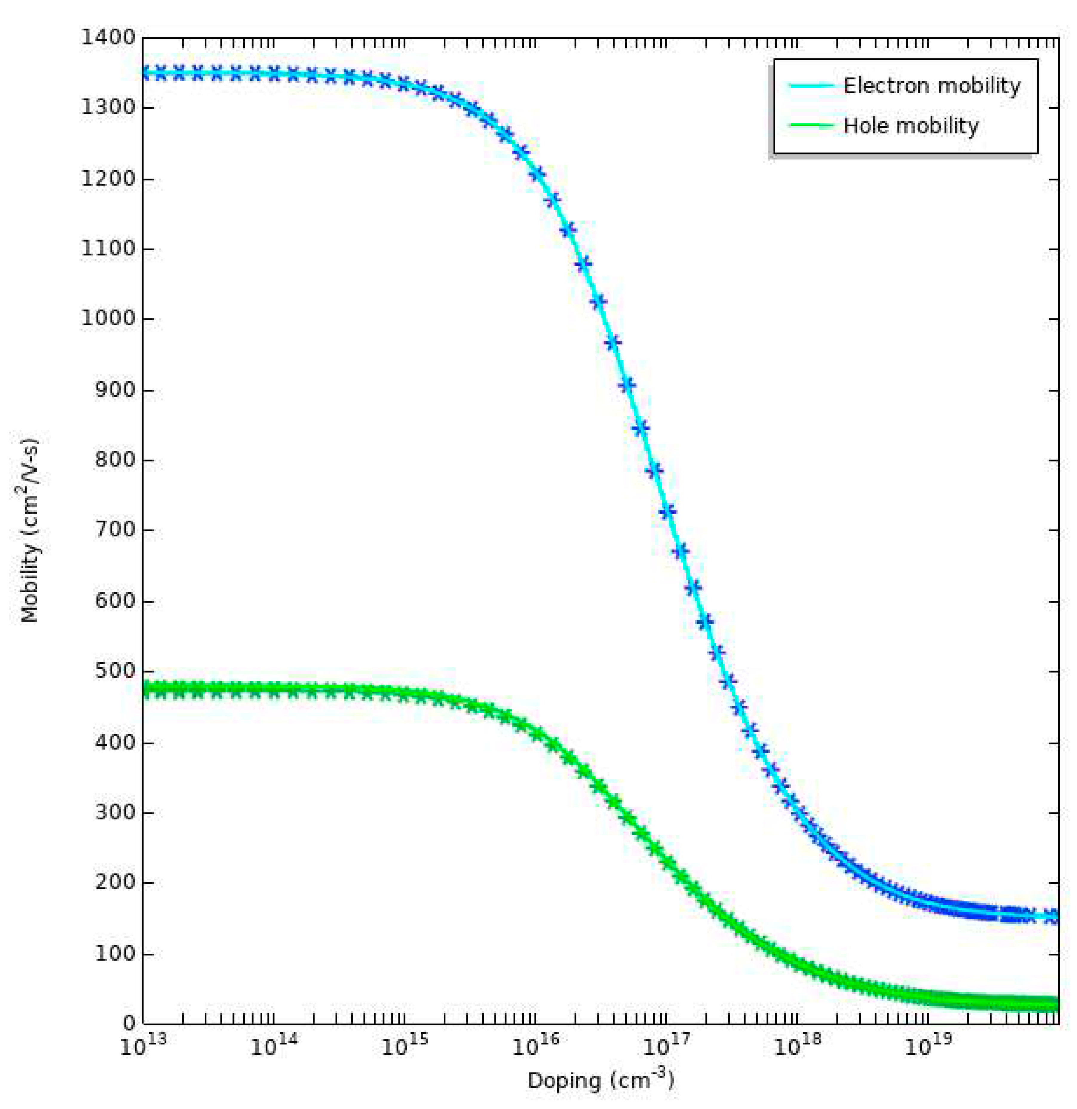
Figure 3.
I-V characteristic of n-ZnO/p-CuGaO2 heterojunction diode at different ionizing dose.

Figure 4.
a. Steady state electric field within a PN diode across various levels of ionization dose.
Figure 4.
a. Steady state electric field within a PN diode across various levels of ionization dose.
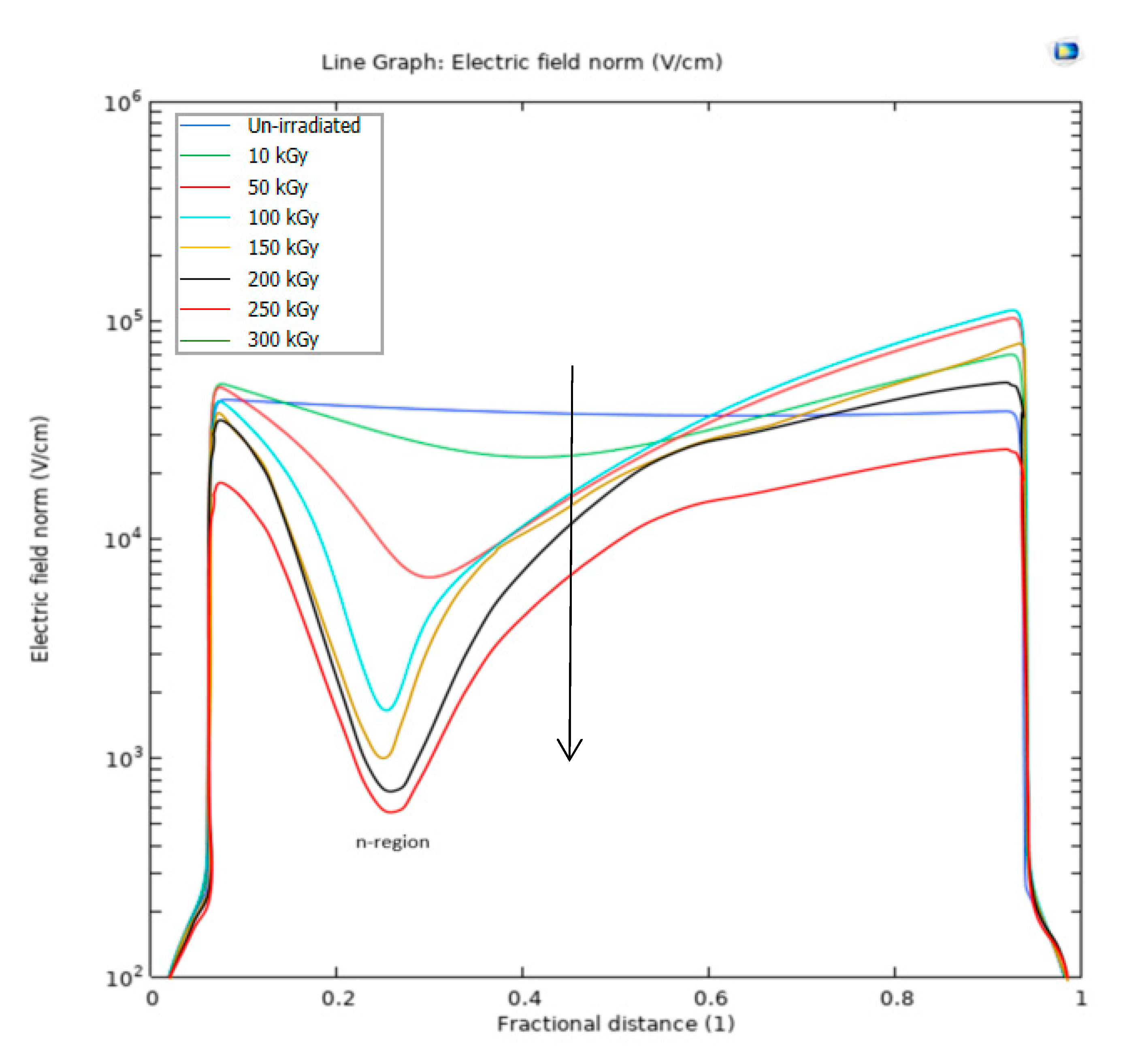
Figure 4.
b. Steady Hole distribution in PN diode for several ionization doses.
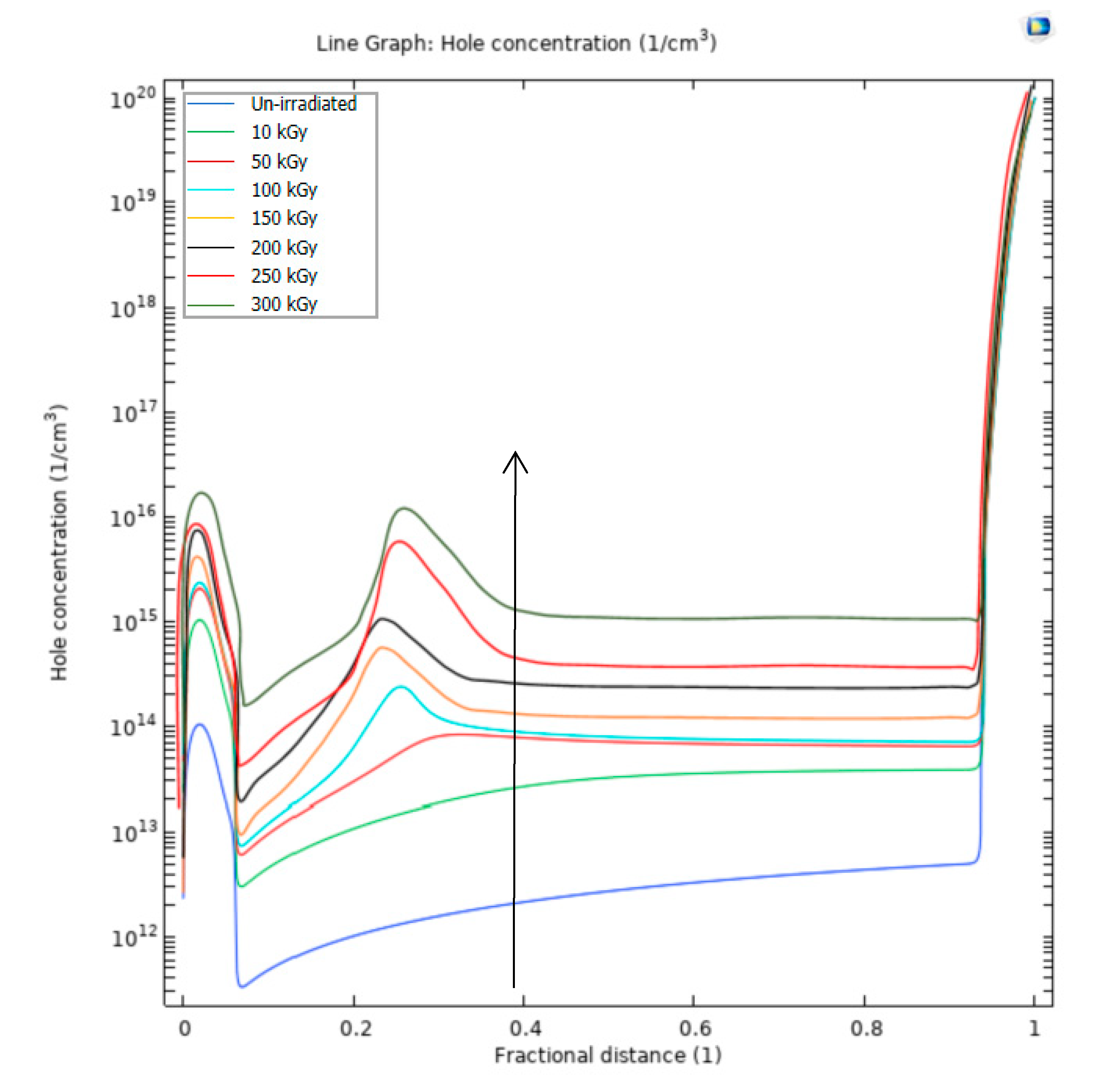

Table 1.
Electrical properties of un-irradiated and irradiated n-ZnO/p-CuGaO2 heterojunction.
| dV/dlnI | ||||
| Samples | Turn-on-Voltage, | Ideality Factor, | Series Resistance, | Barrier Height, |
| V | n | Rs (Ω) | ɸ(eV) | |
| Un-Irradiated(kGy) | 1.5 | 2.80 | 1680.0 | 0.63 |
| 10 | 1.6 | 30.27 | 1859.0 | 0.56 |
| 50 | 1.8 | 47.94 | 4796.0 | 0.56 |
| 100 | 3.2 | 58.22 | 8596.0 | 0.61 |
| 150 | 4.5 | 68.72 | 36578 | 0.58 |
| 200 | 4.7 | 88.16 | 52348 | 0.45 |
| 250 | 5.2 | 97.162 | 67748 | 0.41 |
| 300 | 7.3 | 102.162 | 102112 | 0.39 |
Disclaimer/Publisher’s Note: The statements, opinions and data contained in all publications are solely those of the individual author(s) and contributor(s) and not of MDPI and/or the editor(s). MDPI and/or the editor(s) disclaim responsibility for any injury to people or property resulting from any ideas, methods, instructions or products referred to in the content. |
© 2023 by the authors. Licensee MDPI, Basel, Switzerland. This article is an open access article distributed under the terms and conditions of the Creative Commons Attribution (CC BY) license (http://creativecommons.org/licenses/by/4.0/).
Copyright: This open access article is published under a Creative Commons CC BY 4.0 license, which permit the free download, distribution, and reuse, provided that the author and preprint are cited in any reuse.


