Submitted:
01 July 2025
Posted:
02 July 2025
You are already at the latest version
Abstract
Tantalum nitride (TaN) is a typical transition metal nitride with the characteristic of adjustable resistivity over a wide range. Low-resistance TaN even exhibits a resistivity similar to that of metals. Since the electrical resistance of the compound can influence the secondary electron emission (SEE) behaviors, this study aims to investigate the relationship between the electrical resistivity and the SEE regularities of TaN films. We prepared five groups of TaN films by varying the N₂ partial pressure during sputtering. Microstructural analysis revealed that the film thickness ranged from approximately 197 to 281 nanometers. Results obtained by X-ray photoelectron spectroscopy (XPS) indicated that the Ta:N atomic ratio of the TaN films ranged from approximately 0.53 to 0.87. Additionally, XPS results indicated the presence of non-adsorbed oxygen on the surface of the TaN films, and Further accurate XPS analysis revealed that there was TaNO compounds formed on the TaN surfaces under the influence of oxygen. Square resistivity tests show that the resistivity of the TaN films ranges from 5.67×10⁻³ to 2.43 Ω·cm. Furthermore, the lower the Ti:N atomic ratio is, the lower the electrical resistivity of the TaN film becomes. SEE coefficient (SEEC) results indicate a clear positive correlation between SEEC and electrical resistivity of the TaN films, meaning that smaller SEEC can be acquired by film with lower electrical resistivity. When the N₂ gas flow rate was 16/0 sccm, SEEC of the TaN film was the smallest/largest, with a SEEC maximum of about 1.88/2.25. The research provides valuable reference for expanding the application of TaN films in engineering scenarios involving electrical resistivity adjustment and SEE applications.
Keywords:
tantalum nitride
; electrical resistivity
; secondary electron emission
; atomic ratio
1. Introduction
Tantalum Nitride (TaN) is a versatile, high-performance ceramic material that plays a vital role in key technologies in areas as diverse as optoelectronic devices, integrated circuit manufacturing and aerospace [1,2,3,4]. TaN possesses excellent physical properties including thermal stability, chemical inertness, diffusion barrier, tunable resistivity and high stiffness, making it ideally suited for film applications where reliability is critical under extreme conditions [3,4,5], as well as, TaN also has applications in micro electromechanics and energy harvesting [5,6,7]. In the field of semiconductor manufacturing, TaN films act as a diffusion barrier in copper interconnect technology to prevent the rapid diffusion of copper atoms into the surrounding silicon, this advantage is a capability that is critical for nanoscale feature sizes in advanced chips [8,9,10]. In addition, TaN is a key material for metal gates in transistors, acting as a stable electrode and functional layer for power function tuning in MOSFETs [10,11,12]. Besides, by combining the stability with metallic/semi-metallic conductivity of TaN in certain phases, TaN is considered to be an ideal candidate for electrodes in a variety of miniature sensors used in harsh environments [13,14]. In coating engineering, TaN films excel as protective coatings against high temperatures, thermal cycling, radiation exposure, friction and oxidizing environments [15,16]. Besides, TaN coatings can be used as functional layers on electronic components in satellites and spacecraft to protect them from the damaging effects of cosmic rays and solar radiation, as well as, the chemical inertness and oxidation resistance of TaN ensure long-term performance stability in challenging environments [16,17,18].
Many transition metal nitrides have physical and chemical properties similar to those of TaN [3], among which, titanium nitride (TiN) is a nitride with extremely similar physical and chemical properties to those of TaN, including adjustable metal-like conductivity [19], wear-resistant and high-temperature-resistant physical properties [20,21,22], and good chemical stability that does not easily react with other substances [22]. In addition, the low secondary electron emission (SEE) coefficient (SEEC) property of TiN makes it widely used in scenarios where secondary electron multiplying discharges are suppressed [23,24,25,26]. Typical scenarios where TiN is applied to reduce SEEC include, suppressing electron cloud generation in particle accelerators[23], and mitigating multipactors in space microwave systems [25,26]. Since TaN has similar physical properties with TiN, it is curious for us to see if TaN can be used as a new SEEC modulating functional material in a variety of scenarios involving electron emission. From previous studies, we know that the SEEC of films partly depends on their resistance characteristics [27]. Although there has been very little research on the electron emission phenomenon of TaN films, there have been reports on electrical resistance control on TaN films [28,29,30]. For example, in 2004, Lal et al. investigated the resistive properties of TaN thin films deposited by ion beam assisted deposition, and they found the non-metallic properties of TaN are attributed to nitrogen-induced carrier localization effects, as well as, they also achieved a change in resistivity from 789 μΩ·cm to 2882 μΩ·cm by controlling the nitrogen content [28]. In 2018, by employing the technology of 30 keV nitrogen ion implantation, Ramezani et al achieved a controllable increase in the resistivity of TaN film from 182.7 mΩ·cm to 272.6 mΩ·cm, revealing the synergistic control mechanism of nitrogen doping dose on TaN phase transformation, surface morphology, and electrical properties [29]. In 2021, Jiang et al. researched the electrical resistance control characteristics of TaN films under the influence of oxygen, it was concluded that the oxygen doping strategy enabled precise control of the resistivity of cubic TaN thin films over seven orders of magnitude, namely, from 5.3×10⁻⁴ S/m to 4.1×10³ S/m [30]. The above studies show that TaN exhibits excellent resistive tunability. Although there are few reports on electron emission of TaN, we expected that TaN would also exhibit a unique SEEC regularity as TiN act as.
In this work, by controlling the process parameters, we investigated the composition, electrical resistivity, and SEEC regularity for TaN, to reveal the tunability of electrical resistivity, and see whether it can be used in certain applications involving electron emission. We conducted a systematic study on the influence of gas flow rate on the physical properties of TaN films, including the effect of N₂ flow rate on the film composition. Additionally, we presented the experimental relationship between the elemental composition and the electrical resistivity of TaN films, as well as, experimentally explored the influence of film electrical resistivity on the SEEC. To theoretically explain the experiment results, the potential physical mechanisms by which free electron concentration affects the SEEC process was discussed. This research provides valuable insights for expanding the application of TaN materials in the field of vacuum electron emission.
2. Results and Discussion
2.1. Surface and Fracture Surface Characterization of TaN Film Samples
Five TaN film samples, denoted as #1-#5, were fabricated by reacting sputtering process, and the gas flow rate of #1-#5 TaN film samples were N2:Ar=0:16, 4:16, 8:16, 12:16, 16:16, respectively. Figure 1 shows the surface morphologies and fracture surfaces of TaN film samples characterized by scanning electron microscopy (SEM) at the same magnification. Figure 1a-d are the SEM photos of top view for the #1, #2, #3, #5 TaN film samples, where Figure 1e-h are the corresponding fracture surface images. Comparing the surface morphologies of the TaN film samples in Figure 1, it can be seen that the gas flow rate of N2:Ar during the sputtering process has some effect on the surface morphology of the TaN film samples. To be specific, as shown in Figure 1a, it can be found that when N2 is not fed into the preparation process, namely N2:Ar=0:16, the surface of TaN film has many raised irregular structures, the size of the crystal grains is about a few tens of nanometers and the crystal boundaries between the crystal grains are pronounced. When the gas flow rate goes higher, N2:Ar=4:16, as shown in Figure 1b, the crystal grain size becomes significantly smaller, and on closer inspection, the crystal grain size is about tens of nanometers, and the boundaries between the crystal grains are no longer obvious. As for the cases that gas flow rate of N2:Ar≥8:16, no visible crystal grains or crystal boundaries can be observed on the surface in Figure 1c-d, except for tiny contamination particles. The above results indicate that the crystal grain size of the formed TaN films is large and crystal grain boundaries are obvious when the N2 gas flow rate is low in the process of this experiment. Conversely, when the N2 flow rate is increased, the grain size of the formed TaN films becomes smaller.
The thickness information of the TaN film samples can be obtained from the fracture surface images in Figure 1e-h, which has been marked with a green line segment. Via the software embedded in the SEM system, we acquire the approximate thickness values of #1-#5 TaN film samples, namely, 281 nm, 251 nm, 239 nm, 213 nm and 197 nm, respectively. Here, we find that for TaN samples #1-#5, the thickness values of the prepared film samples become progressively smaller as the N2 gas flow rate rises for the same period of time. This result suggests that the rise in N2 gas flow rate slows down the sputtering rate. In fact, during the experiment, N2 is the main gas involved in the reaction, while Ar atoms are the main actors involved in the ionization and collisional sputtering process, so the decrease of Ar gas concentration slows down the sputtering rate, resulting in a decrease in the film thickness in the same time.
2.2. Elemental Content Characterization of TaN Film Samples
In addition to the surface morphology and fracture surface characterization using SEM, we have also analyzed the surface elements of the prepared TaN films using energy dispersive X-ray spectroscopy (EDS), an accessory hardware to SEM. Figure 2 demonstrates the EDS test results of the TaN film samples, where Figure 2a shows the results of the EDS spectra of #1-#5 TaN film samples, Figure 2b shows the morphology of the EDS test region of sample #3, and Figure 2c-e show the distribution of the three elements, Ta, N, and O inside sample #3. Table 1 gives the elemental proportions in different TaN films obtained from EDS analysis. Figure 2a indicates that the peak intensity of each element in the EDS spectrum of sample #1 is significantly higher than other samples, which is due to the fact that the thickness of #1 is greater than other samples and the depth of detection of EDS is greater than the thickness of the films. Comparing the elemental distributions in Figure 2c-e, it is clear that the elemental densities of Ta and N in sample #3 are significantly higher than those of O. This indicates that the O content is very low within the detection depth range of EDS, which is consistent with the results in Table 1. Besides, From Table 1, it can be seen that Si element can be detected by EDS, and it comes from the substrate since the detecting depth of EDS is typically on the sub-micron to micron scale, exceeding the thickness of the TaN film samples. Table 1 shows that the Si element accounts for a considerable proportion of the direct EDS test results, and here, in order to more accurately analyze the changes in the composition of the film elements, we need to remove the Si element from the test results.
By removing the element Si from the test results in Table 1, we obtained the ratios of the four elements Ta, N, C, and O in Table 2. Table 2 shows that the sputtered TaN film samples are mainly composed of four major elements, namely, Ta, N, C, and O, and the proportions of the various elements change significantly with the change of the proportion of N2 in the gas mixture. The presence of the C and O elements suggests that there is some gas adsorption and organic contamination on the surface of the sample before it enters the XPS analysis chamber. Removing the effects of C and O, we can see that for samples #1-#5, there is a significant increase in the content of N element and a significant decrease in the content of Ta element in the films with the increase of N2 gas flow rate during the preparation process. The Ta:N atomic ratio data is given in the last column of Table 2, which also shows the variation of the elemental ratios of Ta and N elements in the films, namely, the Ta:N atomic ratio in the films is 0.739 when the N2 gas flow rate is 0, and the Ta:N atomic ratio in the films decreases to 0.254 when the N2 gas flow rate is 16 sccm. The results of the above analysis of the elemental ratio data show that the prepared films meet the expectations of our designed experiments.
2.3. Accurate Composition Characterization of TaN Film Samples
X-ray photoelectron spectroscopy (XPS) is another precise method used for surface elemental analysis, with detection depths typically in the range of a few to a dozen nanometers. XPS technology is therefore well suited for the quantitative analysis of the most superficial elements for the prepared TaN film samples. Figure 3 shows the XPS test results of the #1-#5 TaN film samples. From Figure 3a, we are able to observe the binding energy positions corresponding to the various elemental characteristic peaks, as well as the intensity of the various characteristic peaks. In the XPS spectra in Figure 3, the characteristic peaks at binding energies of about 396 eV, 25 eV, 283 eV and 530 eV are corresponding to N 1s, Ta 4f, C 1s and O 1s respectively, as well as there are some other characteristic peaks of Ta, mainly including Ta 4d and Ta 4p. Besides, the existence of two characteristic peaks of C and O indicates the adsorption of organic contamination on the film surface. By observing the intensity of the characteristic peaks in the XPS spectrum of Figure 3a, we know that as the N2 gas flow rate rises, the proportions of the elements N and Ta also increase significantly, and there is a significant decrease in the proportion of O. Meanwhile, the characteristic peak intensity of element C does not change much, indicating that the amount of organic contamination on the surface of the five film samples is relatively close. From the fine spectral analysis of elemental N in Figure 3b, Ta in Figure 3c and O in Figure 3d, it can be seen that O not only exists in the form of organic contamination and impurity gas adsorption, but also combines with elemental Ta to form compound Ta2O5. The results in Figure 3b-d indicate that the TaN film samples we prepared in this work are actually in the form of TaNO.
For the XPS results of five TaN films, the atomic percentage data of all elements Ta, N, C, and O tested by XPS are listed in Table 3. Comparing the XPS elemental test results in Table 3 with the EDS elemental test results in Table 2, we can see that the proportion of O elements measured by XPS is significantly higher. Since the detecting depth of XPS is in the range of a dozen nanometers from the surface, the results of the comparison between Table 2 and Table 3 indicate that the oxidation of TaN films to form TaNO thin layer just occurs at the outermost surface of the TaN film, as well as, the thickness of TaNO is about several nanometers. In addition, the data in Table 3 show that the content of elemental C in the five TaN films is similar, indicating that the degree of organic contamination on the sample surfaces is approximate. Besides, for samples #1-#5, the Ta:N atomic ratio gradually decreases with the increase of N2 gas flow rate, indicating that increasing the gas flow rate of N2 is effective for the adjustment of film composition.
2.4. Characterization of Electrical Resistivity Property for the TaN Film Samples
In addition to the microanalysis of the TaN thin film samples, we also performed a characterization and analysis of the electrical resistivity property of the samples. It should be noted that since Si is a semiconductor substrate, the accuracy of the test results will be affected when using the four-probe method for square resistance testing. Here, in order to eliminate the effect of the substrate on the test results, we use a glass sheet as the substrate for the square resistance test of TaN film samples. The values of physical property parameters of five TaN film samples are given in Table 4, where the thickness of the films has been read out from the analysis results of SEM photos in Figure 1. The square resistance of the TaN film samples is measured by the four-probe method. Finally, the electrical resistivity, ρ, of the TaN film samples can be calculated by the following equation,
Here, R is the square resistance, and t refers to the film thickness. The calculated film electrical resistivity is given in the last column of Table 4.
From the data in Table 4, it can be seen that with the increase of N2:Ar gas flow rate during the sputtering process, the electrical resistivity also tends to decrease. Merely, it is clear that gas flow rate is not a direct factor that varying the film electrical resistivity. Through the analyses in Table 2 and Table 3, we can see that the gas flow rate directly affects the elemental ratio of Ta and N during the formation of TaN films, and according to the reference [29,30], it is known that the elemental ratio inside the TaN film composition will greatly affect the film electrical resistivity. For this reason, we plotted Figure 4 to depict the dependence of electrical resistivity on the film elemental composition. Figure 4a-b demonstrate the effect of N:Ar gas flow rate and XPS-measured Ta:N atomic ratio on the electrical resistivity of TaN films, respectively. From Figure 4b, it can be concluded that the element proportions in TaN films has a very significant effect on film electrical resistivity, which varies by up to three orders of magnitude over the range of process parameters used in this work. To be specific, Figure 4b indicates that the lower Ta:N atomic ratio results in lower electrical resistivity of the TaN films, and a lowest electrical resistivity of 2.75×10⁻³ Ω·cm was obtained at Ta:N=0.52 (XPS results) when N2:Ar=12:16.
2.5. SEE Characterization of TaN Film Samples
SEE is an important physical phenomenon in vacuum environment. SEE phenomenon involves a variety of vacuum scenarios, such as electron multipliers [32], space electrostatic discharge [33], secondary electron multiplication discharge [34], space dielectric surface charging and discharging [35], and other typical scenarios. SEEC is a physical parameter used to measure the number of secondary electrons induced by collisions between electrons and solid surfaces. SEEC is defined as the ratio of the number of secondary electrons induced by collisions between electrons and solid surfaces to the number of initially incident electrons. Considering that the TaN films studied in this work have similar electrical resistance tunable properties as TiN, as reported in reference [30], we believe that the resistance tunable properties of TaN films may have applications in SEEC modulation studies like TiN [23,24,25,26]. In addition, TaN films may have applications in low SEEC scenarios since they have low electrical resistance properties similar to TiN films [27,30,31]. Based on the above considerations, we believe that there is a large potential for the research targeting the SEEC of TaN film samples.
The measured SEEC curves of TaN film samples are shown in Figure 5a. Figure 5 shows that as the primary electron energy rises, the SEEC curve shows a tendency to rise and then fall, which is due to the different abilities of primary electrons with different energies to excite internal secondary electrons in their paths, as well as the different probabilities for these internal secondary electrons to escape to the surface and eject as secondary electrons. In fact, when the primary electron energy is low (tens of eV), the number of internal secondary electrons that can be excited by the incident electrons is very small, resulting in a low SEEC. With the increment of the primary electron energy, the primary electron enters the solid interior and generates energy loss on its motion path, and more internal secondary electrons can be excited, resulting a SEEC increment. However, when the energy of the primary electrons continues to rise, although it can excite more internal secondary electrons on the motion path, these internal secondary electrons have longer distance away from the surface. This long travelling distance leads to the fact that these internal secondary electrons do not easily travel to the surface and escape to become outgoing secondary electrons, as a result, the probability of electron ejection decreases in this case. Based on the above discussion, the phenomenon that the SEEC curve shows a tendency of first increasing and then decreasing with the increase of incident energy, is determined by a combination of both internal electron excitation and escape processes.
Figure 5a shows that as the N2:Ar gas flow ratio increases, the SEEC of TaN film samples gradually decreases and eventually tends to stabilize. Specifically, the SEEC maximum of the prepared TaN film sample is 2.23 when the N2 gas flow rate is 0, and the SEEC maximum of the prepared TaN film sample decreases to 1.89 when the N2 gas flow rate reaches 16 sccm. In fact, the decrease of the SEEC of the TaN film originates from the decrease of the film electrical resistivity due to the rise of the N2 gas flow rate. In other words, as the N2 flow rate rises, the Ta:N atomic ratio in the film decreases, as a result, the electrical resistivity decreases, and leading to the decrease of SEEC. Via the perspective of the physical process of electron-matter interaction, the phenomenon of SEEC decrease induced by electrical resistivity variation can be explained as follow. Since the motion of excited internal secondary electrons is sharply affected by the scattering with internal free electrons, then the probability that scattering occurs determines the probability that the internal secondary electrons are ejected. Specifically, the greater the scattering probability of internal secondary electrons is, the more severe the energy loss shows, and the lower its ejection probability is, which is macroscopically manifested by a smaller SEEC. Therefore, the concentration of free electrons is an important factor in determining the electrical resistivity of the TaN films, namely, the higher concentration of free electrons means the lower electrical resistivity; conversely, the lower concentration of free electrons means the higher electrical resistivity. Therefore, for #1 TaN sample with relatively higher electrical resistivity, its SEEC is higher, while for #4 and #5 TaN samples with relatively lower electrical resistivity, its SEEC is also lower. The results in Figure 5b show an approximately linear increase in SEEC maximum for the exponential growth of TaN electrical resistivity, which demonstrates that there may be an underlying mathematical relationship between electrical resistivity and SEEC for TiN film samples.
3. Methods
3.1. TaN Film Preparation
TaN thin films were prepared in the laboratory by direct current magnetron sputtering, N-type silicon wafers and glass sheets were employed as the substrates for film deposition. Prior to preparation, the substrate surface was cleaned with acetone, alcohol and ultrapure water to remove any contaminants that may be present on the substrate. The sputtering material used in the laboratory is a 99.99% pure TaN target with a diameter of 50.8 mm and a thickness of 3 mm. The gas pressure inside the sputtering chamber is pumped to below 5×10⁻⁴ Pa to reduce the negative influence of other gases on the sputtering process. Before the process of sputtering, there are two gases introduced, namely, high-purity Ar and high-purity N2. Here, high-purity Ar (99.99% purity) is indispensable for the working gas of magnetron sputtering ionization glow, while high-purity N2 (99.99% purity) is used as a reaction gas. In this experiment, the elemental percentage in TaN films is mainly changed by adjusting the ratio of gas flow through N2 and Ar, so as to study the effect of elemental percentage on the electrical resistivity and SEEC of TaN film samples. During the sputtering process, the partial pressures of N2 and Ar in the vacuum chamber were controlled by two gas flow meters, the sputtering time was controlled to be 120 min, and the substrate was not heated during the sputtering process. Five samples were prepared according to the flow rate of N2 and Ar, from 0:16 to 16:16, during the sputtering process. Other detailed experimental parameters have been given by Table 5.
3.2. Physical Characterization Methods
The surface morphology and thickness of the TaN films were characterized using a SEM (Zessi Gemini 500, Oberkochen, Germany). The elemental composition of the coatings is analyzed by EDS (Oxford Instrument, accessory of Gemini 500, Oberkochen, Germany). Additionally, the surface element composition of the TaN films was characterized by XPS (Thermo Fisher ESCALAB Xi+, Al Kα, Massachusetts, USA). The square resistance of TaN films was obtained by the technology of four-probe test (Nuoleixinda, RTS-9, Tianjin, China).
SEEC is usually calculated by measuring the secondary electron current and incident current due to the difficulty of counting the number of electrons. The SEEC test principle applied in this work can be found in reference [36].The specific measurement principle and steps of the SEEC test equipment can be briefly described as follows. Firstly, the primary electrons are incident perpendicular to the sample, and the excited secondary electrons are captured by the positively biased collector, at which time the secondary electron current ISE can be measured. For dielectric samples with surface charge accumulation after SEE process, compare the sample surface potential VS with the ground potential VB, if VS>VB, then the neutralizing gun 1 emits electrons to eliminate the positive charge accumulated on the surface until VS=VB; otherwise, the neutralizing gun 2 is activated and emits electrons with an energy of about 300 eV, at which time the secondary electrons are released. About 300 eV of electrons, then the secondary electron emission process will lead to the accumulation of positive charges on the surface, and the resulting positive charges are neutralized with the electrons accumulated on the original surface until VS>VB, then neutralization gun 2 is switched off, and neutralization gun 1 is activated and removes the positive surface charges until VS=VB; after the surface potential neutralization is completed, the SEEC measurement of the next point of the initial electron energy is initiated. Here, the test sample TaN film in this work is conductor, so it does not involve the neutralization process mentioned above, and after the ISE is obtained from the first step of the test, the SEEC can be calculated directly by combining with the incident electron energy beam current IP by
4. Conclusions
In this work, we studied various physical properties of TaN films obtained by magnetron sputtering, investigated the influence of sputtering N2 partial pressure on film composition, and established the variation regularity in film resistivity and SEEC under the influence of film composition. Through our research, we obtained the following three conclusions. (1) By adjusting the N2 gas flow rate during the sputtering process, it is possible to control the thickness, deposition rate, and elemental composition of TaN films. When the N₂ ratio is relatively low/high during sputtering, the film deposition rate is relatively fast/slow, resulting in TaN films with low/high N content. (2) SEEC results indicate that TaN films prepared with an N₂ partial pressure of 0 exhibit the highest SEEC, with a SEEC maximum of approximately ~2.25; TaN films prepared with an N₂ partial pressure of 16 sccm exhibit the lowest SEEC, with a SEEC maximum of approximately ~1.88. (3) Experimental results show a positive correlation between the SEEC of TaN films and their electrical resistivity. This can be attributed to differences in the probability of internal secondary electrons being scattered due to varying concentrations of free electrons inside the film, resulting in increased/decreased SEEC as electrical resistivity increases/decreases. This work has thoroughly investigated the variation regularity of elemental composition in TaN films under different N₂ partial pressures, as well as the trends in how composition affects electrical resistivity and SEEC. This research holds engineering application value for expanding the use of TaN films in scenarios involving resistivity control and SEEC control.
Author Contributions
Conceptualization, Y.S. and T.W.; methodology, Y.S. and Q.W.; software, Y.S.; validation, Y.S. and T.W.; formal analysis, Y.S. and T.W.; investigation, Y.S. and Q.W.; resources, Y.S.; data curation, Y.S. and Q.W.; writing—original draft preparation, Y.S. and Q.W.; writing—review and editing, Y.S.; visualization, Y.S. and Q.W.; supervision, Y.S; project administration, Y.S.; funding acquisition, Y.S. All authors have read and agreed to the published version of the manuscript.
Funding
This work was supported by the Project of Natural Science Basic Research Program of Shaanxi (Program No. 2024JC-YBMS-525).
Data Availability Statement
The original contributions presented in the study are included in the article, further inquiries can be directed to the corresponding authors.
Conflicts of Interest
The authors declare no conflicts of interest.
References
- Aouadi, S.M. and Debessai, M. Optical properties of tantalum nitride films fabricated using reactive unbalanced magnetron sputtering. J. Vac. Sci. Technol. A, 2004, 22, 1975–1979. [Google Scholar] [CrossRef]
- Bousquet, A.; Zoubian, F.; Cellier, J.; Taviot-Gueho, C.; Sauvage, T.; Tomasella, E. Structural and ellipsometric study on tailored optical properties of tantalum oxynitride films deposited by reactive sputtering. J. Phys. D Appl. Phys. 2014, 47, 475201. [Google Scholar] [CrossRef]
- Patsalas, P.; Kalfagiannis, N.; Kassavetis, S.; Abadias, G.; Bellas, D.V.; Lekka, C.; Lidorikis, E. Conductive nitrides: Growth principles, optical and electronic properties, and their perspectives in photonics and plasmonics. Mat. Sci. Eng. R. 2018, 2018. 123, 1–55. [Google Scholar] [CrossRef]
- Bernoulli, D.; Müller, U.; Schwarzenberger, M.; Hauert, R.; Spolenak, R. Magnetron sputter deposited tantalum and tantalum nitride thin films: An analysis of phase, hardness and composition. Thin Solid Films 2013, 548, 157–161. [Google Scholar] [CrossRef]
- Pihosh, Y.; Minegishi, T.; Nandal, V.; Higashi, T.; Katayama, M.; Yamada, T.; Sasaki, Y.; Seki, K.; Suzuki, Y.; Nakabayashi, M.; Sugiyamaa, M.; Domen, K. Ta3N5-Nanorods enabling highly efficient water oxidation via advantageous light harvesting and charge collection. Energy Environ. Sci. 2020, 13, 1519–1530. [Google Scholar] [CrossRef]
- Ding, C.; Shi, J.; Wang, Z.; Li, C. Photoelectrocatalytic water splitting: significance of cocatalysts, electrolyte, and interfaces. ACS Catal. 2016, 7, 675–688. [Google Scholar] [CrossRef]
- Li, Y.B.; Takata, T.; Cha, D.; Takanabe, K.; Minegishi, T.; Kubota, J.; Domen, K. Vertically aligned Ta3N5 nanorod arrays for solar-driven photoelectrochemical water splitting. Adv. Mater. 2013, 25, 125–131. [Google Scholar] [CrossRef]
- Kolawa, E.; Sun, X.; Reid, J.S.; Chen, J.S.; Nicolet, M.A.; Ruiz, R. Amorphous W40Re40B20 Diffusion-Barriers for [Si]/Al and [Si]/Cu Metallizations. Thin Solid Films 1993, 236, 301–305. [Google Scholar] [CrossRef]
- Holloway, K.; Fryer, P.M.; Cabral, C.; Harper, J.M.E.; Bailey, P.J.; Kelleher, K.H. Tantalum As a Diffusion Barrier Between Copper and Silicon - Failure Mechanism and Effect of Nitrogen Additions. J. Appl. Phys. 1992, 71, 5433–5444. [Google Scholar] [CrossRef]
- Shimada, H.; Ohshima, I.; Ushiki, T.; Sugawa, S.; Ohmi, T. Tantalum nitride metal gate FD-SOI CMOS FETs using low resistivity self-grown bcc-tantalum layer. IEEE T. Electron Dev. 2001, 48, 1619–1626. [Google Scholar] [CrossRef]
- Dekkers, H.F.W; Ragnarsson, L.Å.; Schram, T.; Horiguchi, N. Properties of ALD TaxNy films as a barrier to aluminum in work function metal stacks. J. Appl. Phys. 2018, 124, 165307. [Google Scholar] [CrossRef]
- Thareja, G.; Chun-Wen, H.; Harris, R.; Majhi, P.; Lee, B.H.; Lee, J.C. NMOS compatible work function of TaN metal gate with gadolinium oxide buffer layer on Hf-based dielectrics. IEEE T. Electron Dev. 2006, 27, 802–804. [Google Scholar] [CrossRef]
- Park, H.; Chang, M.; Jo, M.; Choi, R.; Lee, B.H.; Hwang, H. Device Performance and Reliability Characteristics of Tantalum-Silicon-Nitride Electrode/Hafnium Oxide n-Type Metal-Oxide-Semiconductor Field-Effect Transistor Depending on Electrode Composition. Jpn. J. Appl. Phys. 2009, 48, 116506. [Google Scholar] [CrossRef]
- Yeh, Y.H.; Chen, W.C.; Chang, T.C.; Tan, Y.F.; Wu, C.W.; Zhang, Y.C.; Lee, Y.H.; Lin, C.C.; Huang, H.C.; Sze, S.M. Degradation mechanism differences between TiN- and TaN-electrode HZO-based FeRAMs analyzed by current mechanism fitting. Semicond. Sci. Tech. 2023, 38, 085004. [Google Scholar] [CrossRef]
- Smith, BW; Zavyalova, L; Bourov, A; Butt, S; Fonseca, C. Investigation into excimer laser radiation damage of deep ultraviolet optical phase masking films. J. Vac. Sci. Technol. A 1997, 15, 2444–2447. [Google Scholar] [CrossRef]
- Mota, O.U.O.; Araujo, R.A.; Wang, H.Y.; Çagina, T. Mechanical Properties of Metal Nitrides for Radiation Resistant Coating Applications: A DFT Study. 23rd International Conference on the Application of Accelerators in Research and Industry-CAARI 2014. 2015, 66, 576–585. [Google Scholar] [CrossRef]
- Yang, Y.H.; Wu, F.B. Microstructure evolution and protective properties of TaN multilayer coatings. Surf. Coat. Tech. 2016, 308, 108–114. [Google Scholar] [CrossRef]
- Achille, A.; Mauvy, F.; Fourcade, S.; Michau, D.; Cavarroc, M.; Poulon-Quintin, A. Electrochemical Behavior of Tantalum Nitride Protective Layers for PEMFC Application. Energies 2024, 17, 5099. [Google Scholar] [CrossRef]
- Popović, M.; Novaković, M.; Mitrić, M.; Zhang, K.; Bibic, N. Structural, optical and electrical properties of argon implanted TiN thin films. Int. J. Refract. Met. Hard Mater. 2015, 48, 318–323. [Google Scholar] [CrossRef]
- Patsalas, P.; Kalfagiannis, N.; Kassavetis, S. Optical Properties and Plasmonic Performance of Titanium Nitride. Materials 2015, 8, 3128–3154. [Google Scholar] [CrossRef]
- Chin, Y.L.; Chou, J.C.; Lei, Z.C.; Sun, T.P.; Chung, W.Y.; Hsiung, S.K. Titanium nitride membrane application to extended gate field effect transistor pH sensor using VLSI technology, Jpn. J. Appl. Phys. 2002, 40 Pt 1, 6311–6315. [Google Scholar] [CrossRef]
- Gavarini, S.; Bes, R.; Millard-Pinard, N.; Cardinal, S.; Peaucelle, C.; Perrat-Mabilon, A.; Garnier, V.; Gaillard, C. A comparative study of TiN and TiC: Oxidation resistance and retention of xenon at high temperature and under degraded vacuum. J. Appl. Phys. 2011, 109, 014906. [Google Scholar] [CrossRef]
- Suetsugu, Y; Fukuma, H; Ohmi, K; Tobiyaina, M; Flanagan, J; Ikeda, H; Mulyani, E; Shibata, K; Ishibashi, T; Shirai, M; Terui, S; Kanazawa, K; Hisamatsu, H. Mitigating the electron cloud effect in the SuperKEKB positron ring. Phys. Rev. Accel. Beams 2019, 22, 023201. [Google Scholar] [CrossRef]
- Yao, L.; Ouyang, L.J.; Wang, D.; Chen, J.X.; He, Y.N.; Xu, Y.N. Modulation of secondary electron emission from boron nitride composite ceramics. High Volt. Eng. 2023, 49, 3848–3855. [Google Scholar] [CrossRef]
- Meng, X.C.; Wang, D.; Cai, Y.H.; Ye, Z.; He, Y.N.; Xu, Y.N. Secondary electron emission suppression on alumina surface and its application in multipactor suppression. Acta Phys. Sin. 2023, 72, 107901. [Google Scholar] [CrossRef]
- Michizono, S.; Kinbara, A.; Saito, Y.; Yamaguchi, S.; Anami, S.; Matuda, N. TiN film coatings on alumina radio frequency windows. J. Vac. Sci. Technol. A 1992, 10, 1180–1184. [Google Scholar] [CrossRef]
- Wang, D.; He, Y.N.; Cui, W.Z. Secondary electron emission characteristics of TiN coatings produced by RF magnetron sputtering. J. Appl. Phys. 2018, 124, 053301. [Google Scholar] [CrossRef]
- Lal, K.; Ghosh, P.; Biswas, D.; Meikap, A.K.; Chattopadhyay, S.K.; Chatterjee, S.K.; Ghosh, A.; Baba, K.; Hatada, R. A low temperature study of electron transport properties of tantalum nitride thin films prepared by ion beam assisted deposition. Solid State Commun. 2004, 131, 479–484. [Google Scholar] [CrossRef]
- Ramezani, A.H.; Hoseinzadeh, S.; Bahari, A. The Effects of Nitrogen on Structure, Morphology and Electrical Resistance of Tantalum by Ion Implantation Method. J. Inorg. Organomet. P. 2018, 3, 847–853. [Google Scholar] [CrossRef]
- Jiang, C.M.; Wagner, L.I.; Horton, M.K.; Eichhorn, J.; Rieth, T.; Kunzelmann, V.F.; Kraut, M.; Li, Y.B.; Persson, K.A.; Sharp, I.D. Metastable Ta2N3 with highly tunable electrical conductivity via oxygen incorporation. Mater. Horiz. 2021, 8, 1744–1755. [Google Scholar] [CrossRef]
- Kearney, B.T.; Jugdersuren, B.; Culbertson, J.C.; Desario, P.A.; Liu, X. Substrate and annealing temperature dependent electrical resistivity of sputtered titanium nitride thin films. Thin Solid Films. 2018, 661, 78–83. [Google Scholar] [CrossRef]
- Lian, Z.X.; Yao, K.W.; Wang, D.; Zhang, K.Y.; Wang, R.; He, Y.N. Surface potential evolution and DC discharge measurement of the microstrip antenna dielectric under electron beam irradiation. Vacuum 2025, 238, 114270. [Google Scholar] [CrossRef]
- Lian, Z.X.; Wang, D.; Zhu, X.P.; He, Y.N. High-performance microchannel plates based on atomic layer deposition for the preparation of functional layers. J. Phys. D Appl. Phys. 2025, 58, 115106. [Google Scholar] [CrossRef]
- Wang, D.; Mao, Z.S.; Ye, Z.; Cai, Y.H.; Li, Y.; He, Y.N.; Qi, K.C.; Xu, Y.N.; Jia, Q.Q. Ultralow electron emission yield achieved on alumina ceramic surfaces and the application in multipactor suppression. J. Phys. D Appl. Phys. 2022, 55, 455301. [Google Scholar] [CrossRef]
- Wang, J.Y.; Xu, Y.N.; Lian, Z.X.; Wang, D.; Meng, X.C.; Zhou, N.; He, YN. Dynamic evolution investigation on the dielectric surface charging under electron irradiation with various energy distributions. Results Phys. 2024, 57, 107339. [Google Scholar] [CrossRef]
- Cai, Y.H.; Wang, D.; Qi, K.C.; He, Y.N. Measurement of total electron emission yield of insulators based on self-terminating charge neutralization. Rev. Sci. Instrum. 2022, 93, 055103. [Google Scholar] [CrossRef]
Figure 1.
Surface morphology photos and fracture surface photos of TaN film samples characterized by SEM, (a)-(d) are the top view of SEM photos for TaN film samples when N2:Ar=0:16, 4:16, 8:16 and 16:16, as well as (e)-(h) are the corresponding fracture surface photos.
Figure 1.
Surface morphology photos and fracture surface photos of TaN film samples characterized by SEM, (a)-(d) are the top view of SEM photos for TaN film samples when N2:Ar=0:16, 4:16, 8:16 and 16:16, as well as (e)-(h) are the corresponding fracture surface photos.
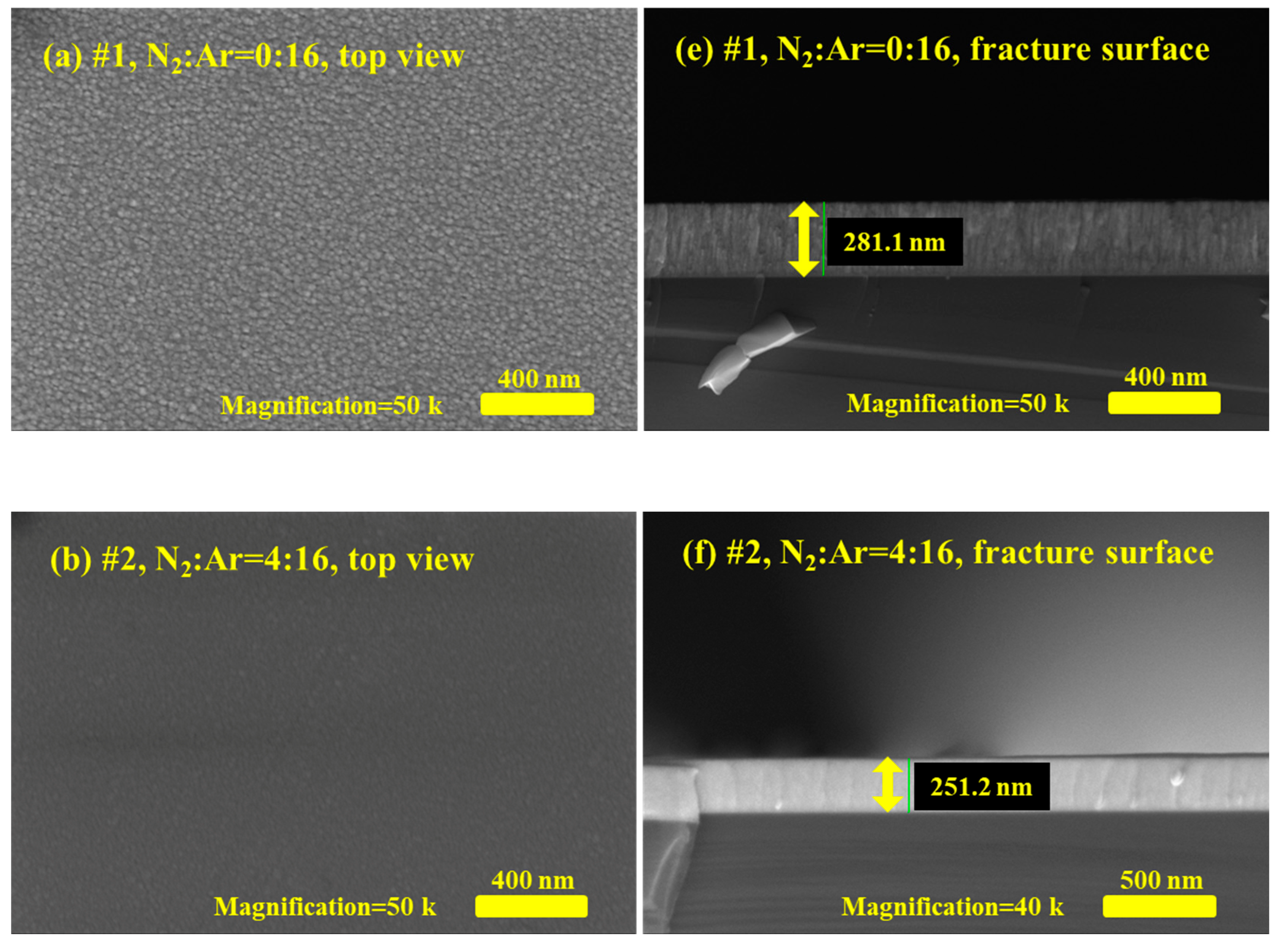
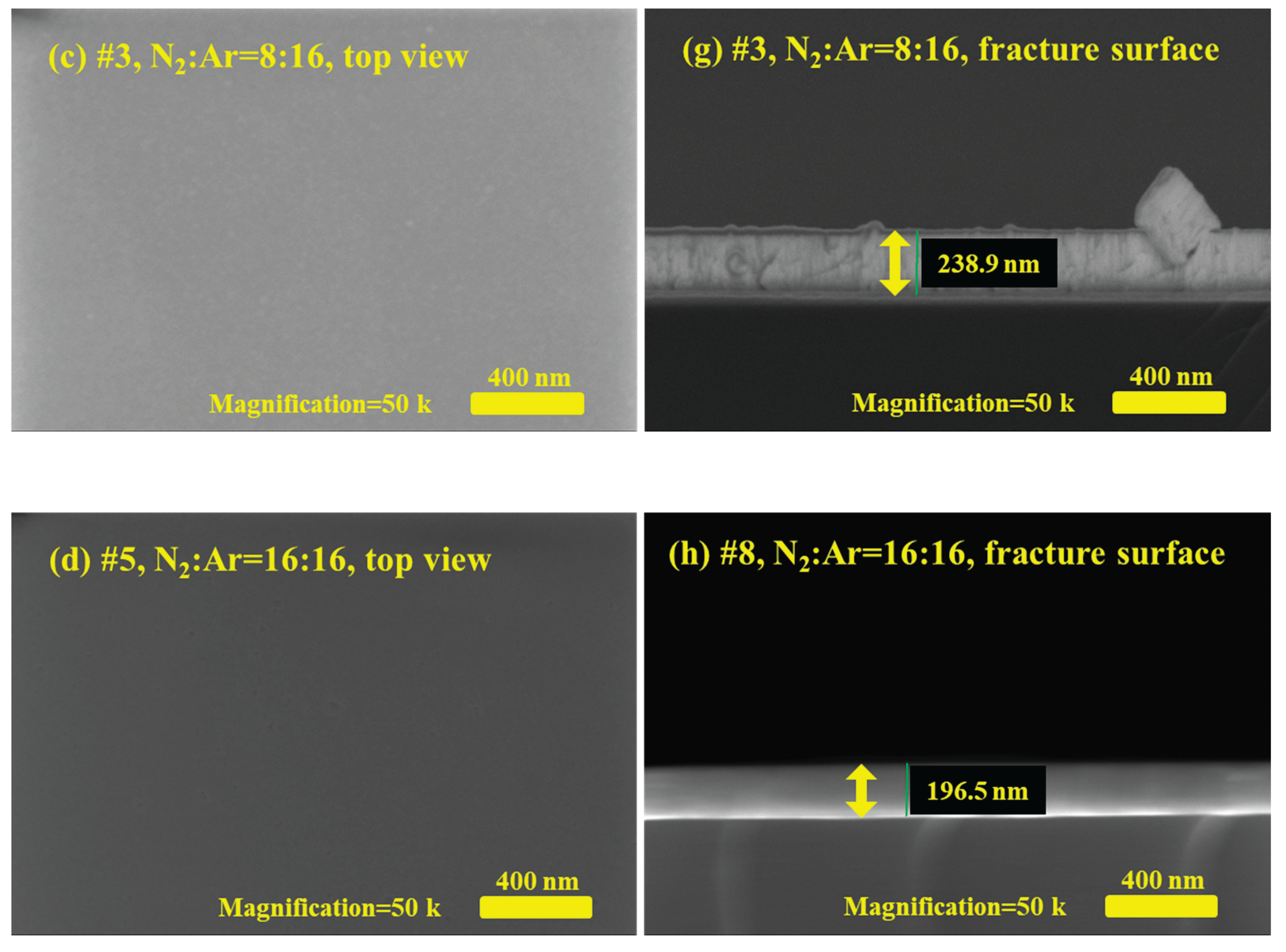
Figure 2.
(a) EDS results of #1-#5 TaN film samples, (b) the EDS testing area of TaN #3 characterized by SEM, (c)-(e) the elemental distribution of Ta, N, and O inside the #3 TaN sample characterized by EDS.
Figure 2.
(a) EDS results of #1-#5 TaN film samples, (b) the EDS testing area of TaN #3 characterized by SEM, (c)-(e) the elemental distribution of Ta, N, and O inside the #3 TaN sample characterized by EDS.
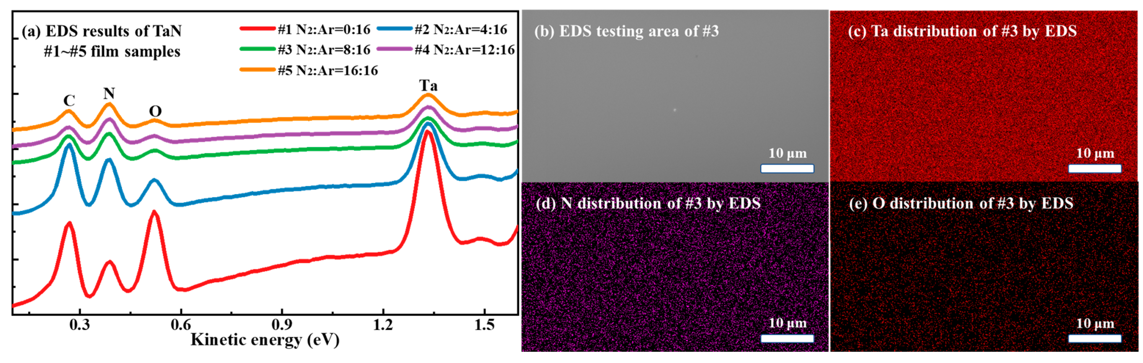
Figure 3.
(a) XPS spectra of the #1-#5 TaN film samples, (b) N 1s fine spectra of TaN film when N2:Ar=8:16, (c) Ta 4f fine spectra of TaN film when N2:Ar=8:16, (d) O 1s fine spectra of TaN film when N2:Ar=8:16, (e) C 1s fine spectra of TaN film when N2:Ar=8:16.
Figure 3.
(a) XPS spectra of the #1-#5 TaN film samples, (b) N 1s fine spectra of TaN film when N2:Ar=8:16, (c) Ta 4f fine spectra of TaN film when N2:Ar=8:16, (d) O 1s fine spectra of TaN film when N2:Ar=8:16, (e) C 1s fine spectra of TaN film when N2:Ar=8:16.
Figure 4.
Variation tendency of electrical resistivity for the prepared TaN film samples, (a) electrical resistivity versus the N2:Ar gas flow rate, (b) electrical resistivity versus the Ta:N atomic ratio.
Figure 4.
Variation tendency of electrical resistivity for the prepared TaN film samples, (a) electrical resistivity versus the N2:Ar gas flow rate, (b) electrical resistivity versus the Ta:N atomic ratio.
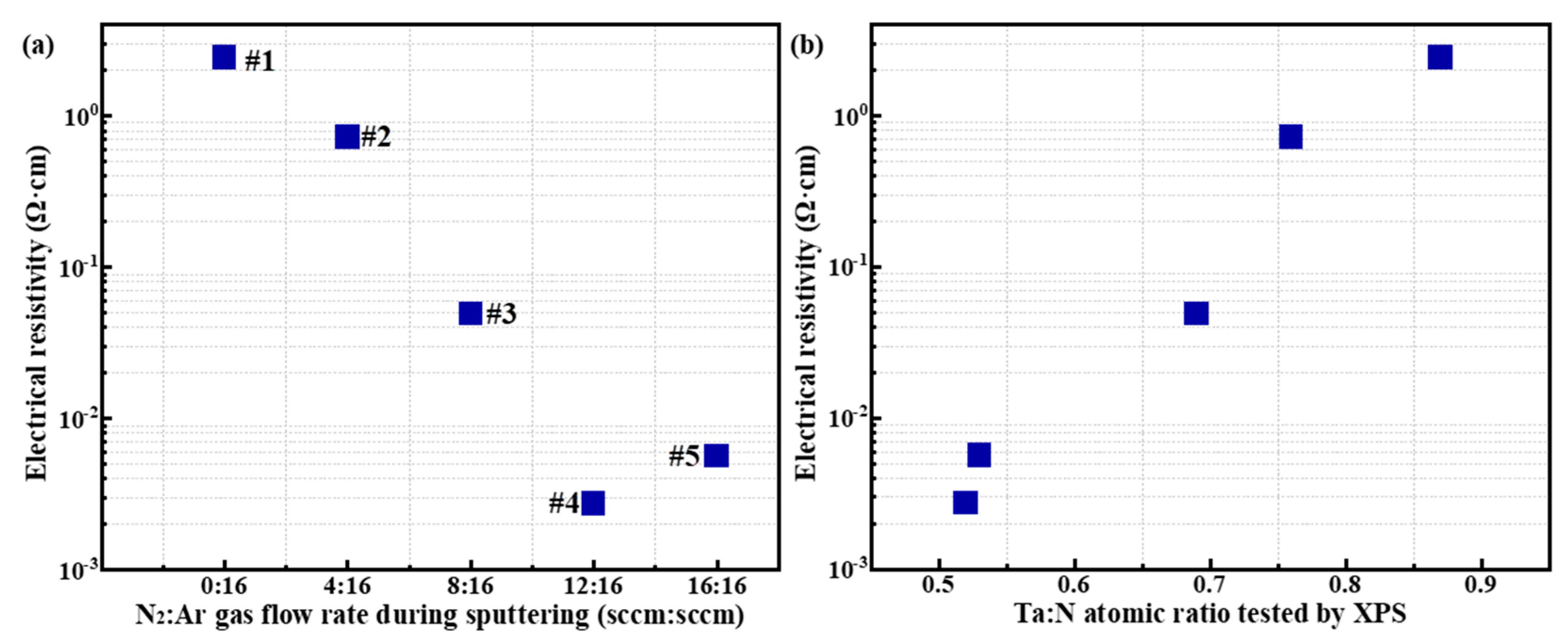
Figure 5.
(a) SEEC of TaN film samples versus the primary electron energy, (b) maximum of SEEC versus the film electrical resistivity.
Figure 5.
(a) SEEC of TaN film samples versus the primary electron energy, (b) maximum of SEEC versus the film electrical resistivity.
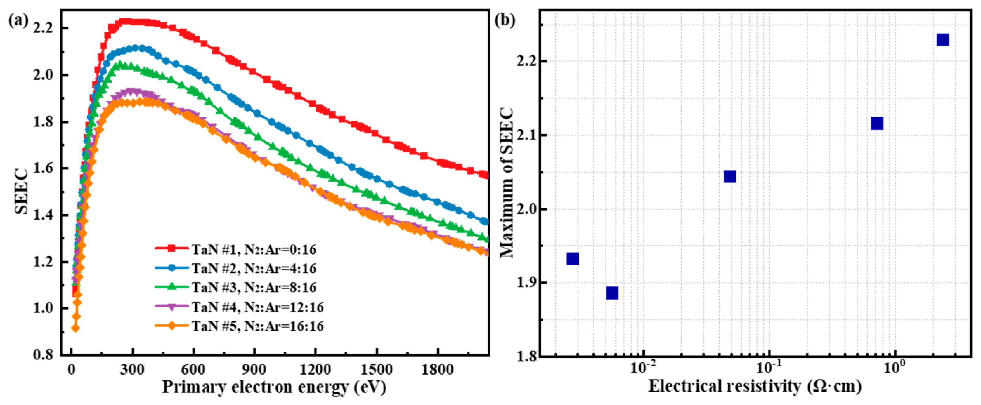

Table 1.
Tested atomic ratio of TaN film samples by EDS, including the substrate Si.
| Sample | N2:Ar | Ta (At%) | N (At%) | C (At%) | O (At%) | Si (At%) |
| #1 | 0:16 | 14.3 | 19.4 | 27.5 | 26.1 | 12.7 |
| #2 | 4:16 | 11.4 | 24.7 | 32.7 | 10.4 | 20.8 |
| #3 | 8:16 | 9.8 | 28.8 | 25.6 | 3.6 | 32.2 |
| #4 | 12:16 | 8.0 | 27.8 | 19.0 | 2.8 | 42.4 |
| #5 | 16:16 | 6.7 | 26.3 | 20.0 | 2.6 | 44.4 |
Table 2.
Tested atomic ratio of TaN film samples by EDS, exclude the substrate Si.
| Sample | N2:Ar | Ta (At%) | N (At%) | C (At%) | O (At%) | Ta:N (At ratio) |
| #1 | 0:16 | 16.4 | 22.2 | 31.5 | 29.9 | 0.739 |
| #2 | 4:16 | 14.4 | 31.2 | 41.3 | 13.1 | 0.462 |
| #3 | 8:16 | 14.5 | 42.5 | 37.7 | 5.3 | 0.341 |
| #4 | 12:16 | 13.9 | 48.3 | 33.0 | 4.8 | 0.288 |
| #5 | 16:16 | 12.0 | 47.3 | 36.0 | 4.7 | 0.254 |
Table 3.
Surface elemental composition of TaN film samples obtained by XPS tests.
| Sample | N2:Ar | Ta (At%) | N (At%) | C (At%) | O (At%) | Ta:N (At ratio) |
| #1 | 0:16 | 12.17 | 13.91 | 34.37 | 39.55 | 0.87 |
| #2 | 4:16 | 13.81 | 18.23 | 35.67 | 32.29 | 0.76 |
| #3 | 8:16 | 14.85 | 21.52 | 33.98 | 29.65 | 0.69 |
| #4 | 12:16 | 10.19 | 19.70 | 38.31 | 31.80 | 0.52 |
| #5 | 16:16 | 12.26 | 23.13 | 34.76 | 29.85 | 0.53 |
Table 4.
Square resistance and electrical resistivity information of TaN film samples.
| Sample | N2:Ar | Thickness (nm) | Square resistance (Ω) | Electricalresistivity(Ω·cm) |
| #1 | 0:16 | 281 | 8.65×10⁴ | 2.43×100 |
| #2 | 4:16 | 251 | 2.89×10⁴ | 7.25×10⁻¹ |
| #3 | 8:16 | 239 | 2.05×10³ | 4.90×10⁻² |
| #4 | 12:16 | 213 | 1.29×10² | 2.75×10⁻³ |
| #5 | 16:16 | 197 | 2.88×10² | 5.67×10⁻³ |
Table 5.
Statistical results of the process parameters for sputtering TaN film samples.
| Sample | N2:Ar (sccm) | Voltage (V) | Current (mA) | Pressure (Pa) | Duration (min) |
| #1 | 0:0 | 800 | 160 | 1.0 | 120 |
| #2 | 0:4 | 800 | 160 | 1.0 | 120 |
| #3 | 0:8 | 800 | 160 | 1.0 | 120 |
| #4 | 0:12 | 800 | 160 | 1.0 | 120 |
| #5 | 0:16 | 800 | 160 | 1.0 | 120 |
Disclaimer/Publisher’s Note: The statements, opinions and data contained in all publications are solely those of the individual author(s) and contributor(s) and not of MDPI and/or the editor(s). MDPI and/or the editor(s) disclaim responsibility for any injury to people or property resulting from any ideas, methods, instructions or products referred to in the content. |
© 2025 by the authors. Licensee MDPI, Basel, Switzerland. This article is an open access article distributed under the terms and conditions of the Creative Commons Attribution (CC BY) license (http://creativecommons.org/licenses/by/4.0/).
Copyright: This open access article is published under a Creative Commons CC BY 4.0 license, which permit the free download, distribution, and reuse, provided that the author and preprint are cited in any reuse.


