Submitted:
14 August 2025
Posted:
15 August 2025
You are already at the latest version
Abstract
Despite recent intensified research efforts in novel alkaline earth oxides (AEOs), there still exist very few studies on their basic structural, optical and phonon characteristics. Exceptional combination of AEOs’ material traits including high thermal conductivity, electrical insulation, wide bandgap, spontaneous polarization at graded interfaces, have made BeO/ZnO strained layer superlattices (SLs) valuable for developing different electro-optical devices. These prospects offered opportunities to integrate SLs into flexible transparent high-performance transistors, ultraviolet light-emitting diodes, biosensors, nano-electronic and nanophotonic modules, etc. Such units are playing vital roles in thermal management solutions to provide safety for nuclear reactors and many medical equipment. In the absence of experimental data on phonon dispersions, dynamic displacements and Raman intensity profiles, systematic simulations are required. Using both elastic continuum and modified linear chain models, we have studied phonon characteristics of short-period BeO/ZnO SLs. Bond-polarizability method is adopted to calculate Raman scattering spectra of graded (BeO)10-D/(Be0.5ZnO0.5O)D/(ZnO)10-D/(Be0.5ZnO0.5O)D SLs by varying interfacial layer thickness from D ≡ 0 to 3 monolayers. The study has showed acoustic phonon branches of SLs weakly affected by interfacing. Low frequency optical modes are shifted upwards in frequency while the high frequency phonons exhibited downward changes up to ~171 cm-1. Increasing D has collectively caused the phonon modes to collapse in the middle of the optical phonon mode region. This has triggered perceiving many prominent Raman scattering features. Such effects are linked to the localization of atomic displacements. Our methodical study markedly insinuated that the Raman intensity profiles of optical modes in strained layer SLs can be well suited for probing the thickness of interfacial layer D, when epitaxially grown samples will become available.
Keywords:
novel BeO/ZnO superlattice
; Raman scattering intensity
; elastic continuum model
; modified-linear-chain model
; interfacial layer thickness
; alloyed inerfaces
1. Introduction
In recent years, many research efforts have been made on novel alkaline earth oxides (AEOs) with the motivations to achieve flexible nano-structured; doped, and composite semiconductor materials [1,2,3,4,5,6]. The AEOs are frequently labelled as II-Os, as they include oxygen (O) atom of group VIA and elements of group IIB (e.g., beryllium Be, magnesium Mg, zinc Zn, cadmium Cd) from the periodic table. Advanced II-O semiconductors generally possess high alkalinity, wide bandgaps, and strong ionic bonding [7,8,9,10,11]. They exist in various crystalline phases ranging from the wurtzite (wz) → zinc blende (zb) → rock salt (rs) structures [1,2,3,4,5,6]. In the realm of materials science, and solid-state physics, the II-Os (e.g., BeO, MgO, ZnO, CdO) and III-Ns (e.g., BN, AlN, GaN, InN) have recently gained significant attention due to their unique electrical and chemical properties. Unlike III-Ns, II-Os can be grown relatively easily. Interestingly, many basic traits of III-Ns have revealed similarities with II-Os (viz., BN→ BeO; AlN, (GaN, InN) → MgO, (ZnO, CdO)). Electronic devices based on II-Os and III-Ns covered nearly the same wavelength range. However, the ZnO (for instance) is considered superior to GaN for fabricating lower threshold laser diodes (LDs), with excitons to operate at higher efficiencies [1,2,3,4,5,6,7,8,9,10,11].
Among other AEOs, the ZnO and BeO show unique electrical, optical, elastic and thermal properties suitable for diverse technological applications. [1,2,3,4,5,6,7,8,9,10,11] Due to large electromechanical coupling with excellent piezoelectric characteristics, ZnO has received considerable attention for fabricating high-frequency acoustic resonance wave devices. Large exciton binding energy ~ 60 meV of ZnO encourages its use for efficient excitonic recombination and plays crucial role for engineering high efficiency and low-cost UV photodetectors [1,2,3,4,5,6]. So far, only a highly textured ZnO film has confirmed optically pumped UV lasing at room temperature (RT) [1,2,3,4,5,6]. Before ZnO could offer a significant contribution to the world of micro- and nano-electronics, it is important to achieve reproducible p-type epilayers [6]. Besides ZnO, the BeO is another distinctive member of the II-Os family. BeO exhibits high thermal conductivity κ, exceptional hardness, large bond strength, high melting point ~2570 ◦C, radiation resistance, and higher dielectric constant, despite having an extremely large bandgap. Combining direct bandgap ZnO ~3.37 eV with BeO ~10.6 eV has encouraged scientists to prepare ternary alloys. This has offered many applications to achieve ultraviolet (UV) UV-LDs, UV light emitting diodes (UV-LEDs), UV detectors, and transparent conducting oxide electrodes (TCOEs). While ZnO is valuable for optoelectronic, biomedical, and antimicrobial devices, BeO exceled its use in thermal management applications to optimize high-frequency, high-temperature electronics. Recently, many BeO-based electronic components are being developed including the UV-LEDs, LDs, gas sensors, and solar cells, etc. [1,2,3,4,5,6,7,8,9,10,11] The material has fulfilled its use in the growing demands for efficient operations of nuclear reactors [12,13,14,15]. BeO has also contributed to lasers for DNA sequencing and tissue analysis. As a TCOE, BeO has been employed in high frequency electronics within displays that require efficient heat dissipation. Recently, BeO-based devices are methodically incorporated: (i) in satellites/aircraft for space exploration, (ii) in nuclear reactors as neutron reflectors, (iii) medical equipment for radiation detection, and (iv) in managing excess heat generation for secured operations of both electronic and optoelectronic systems [7,8,9,10,11].
Substantial improvement has been made recently in the epitaxial growth of II-Os [16,17,18,19,20,21,22,23,24,25,26,27,28]. Commonly used epitaxial methods included the chemical vapor deposition (CVD), metal organic (MOCVD) [16,17], laser ablation [18,19,20], molecular beam epitaxy (MBE), pulsed laser deposition (PLD), atomic layer deposition (ALD), plasma-enhanced ALD (PEALD), plasma-assisted PA-MBE [21,22,23,24,25,26,27,28], etc. Progress in the epitaxial growth process helped achieving high-quality single crystals, ultrathin large area epifilms, BexZn1−xO ternary, BexCdyZn1−x-yO quaternary alloys and low dimensional heterostructures (LDHs) [viz., ZnO/BexZn1−xO multi quantum wells (MQWs), and (ZnO)m/(BexZn1−xO)n superlattices (SLs)]. The integration of BexZn1−xO alloy epifilms in MQWs offered unlimited opportunities to engineer device structures for improving flexible electronics modules. Recently, ZnO/BexZn1−xO based MQWs and SLs are also employed to harness strong excitonic effects to achieve stimulated emission at elevated temperatures for micro-electronic/nano-photonic devices.
Large lattice mismatch between ZnO and BeO is anticipated leading to a large internal strain near the interfacial layers. This could trigger negative impact on the performance of optoelectronic devices [6,7]. In SLs, the in-plane strain depends not only on the structures of constituent layers but also their growth conditions. To ease the lattice strain in BeO/ZnO MQWs and SLs, it is necessary to introduce graded interface between the two integral layers. In heterostructures, such distribution over a wider region can help reduce the stress. For the emergence of rough interfaces at nanometer (nm) scale during epitaxial growth of MQWs, surface segregation has played an important role. Earlier high-resolution transmission electron microscopy (HR-TEM) [29] measurements have reported the appraisal of indium (In) concentration related interfacial gradient thickness in GaN/ In0.43Ga0.57N/Al0.1Ga0.9N. The study [29] has pointed out a typical interface width of 1 nm for GaN/InGaN while more than twice of this value is reported for the InGaN/AlGaN interface [30]. Ab initio calculations are also performed by Boguslawski et al. [31] for comprehending surface segregation energies in wide bandgap III-N alloys. The authors [31] have indicated an order of magnitude larger segregation energies in III-Ns than the conventional III-As (AlAs, GaAs, InAs) alloys and SLs. This difference has been attributed to two major aspects: (a) the chemical bonds are significantly more ionic in nitrides than arsenide’s, and (b) the large mismatch between atomic radii of their cations and anions triggers an increased disorder in wider interfaces. Most importantly, the presence of strained interfacial layers in GaN, AlN, and InN based MQWs, and SLs have shown significant impact on the optical and electrical processes [32,33].
To estimate thickness of thin-film materials, many experimental techniques have been frequently used [29,30,34,35,36,37]. Different methods are adopted including reflectance [34], Raman scatting spectroscopy (RSS) and spectroscopy ellipsometry [35,36,37]. For assessing structural quality and thickness of film interfaces, Raman scattering of phonons is judged as one of the most powerful techniques. Interaction of incident and scattered light with interfaces cause interferences that lead to the variations of Raman intensity profiles [34,35,36]. In each material the observed Raman signatures are unique. In multilayer systems, such features are known to vary non-monotonically with the thickness of different layers. The observed Raman scattering intensity depends on the incident excitation wavelength of laser source, power, detector efficiency, gain, and integration time, etc. If experimental parameters are kept consistent between measurements, the intensity of Raman signal could potentially be used as a measure of estimating film thickness. It is simply because the interference patterns change with film textures, affecting the amount of light scattered and detected in Raman scattering studies. Observed enhanced intensity features in Raman spectroscopy has made it easier to analyze, comprehend the structural and optical properties of heterostructures. Like HR-TEM, RSS has been frequently exploited to confirm the role of interfacial effects in arsenide and nitride-based MQWs [32,33,34,35]. For BeO/ZnO SLs neither the HR-TEM nor RSS studies are available in the literature.
Theoretical methods of varying complexity [38,39,40,41,42,43,44,45,46,47,48,49,50,51,52] have been used to study the phonon dispersions, atomic displacements and Raman intensity profiles in semiconductor SLs. For extracting phonon characteristics, the most comprehensive technique is based on an ab initio local density functional (LDF) approach [50,51,52]. Phenomenological models [38,39,40,41,42,43,44,45,46,47,48,49], though less fundamental than LDF, are quite feasible for examining the vibrational mode behavior in SLs [38,39,40,41,42,43,44,45,46,47,48,49]. Three basic methods are frequently employed: These are: (a) elastic continuum model (ECM) [53], (b) linear chain model (LCM) [38,39,40,41,42,43,44,45,46,47,48,49], and (c) transfer matrix method (TMM) [54]. Although ECM [53] described folding of acoustic phonon branches in SLs, an LCM [38,39,40,41,42,43,44,45,46,47,48,49] has allowed the calculations of acoustic and optical phonon dispersions. The LCM revealed how interfaces between different layers has affected the phonon mode behavior in SLs. Rigorous treatment by TMM has also been used recently to calculate Raman spectra for assessing multilayer thin film thickness [54]. Barker et al. [38] were the first to adopt an LCM approach by considering nearest neighbor (NN) interactions to explore the lattice dynamics of GaAs/AlAs SLs. The method [38] is considered effective in the frequency region where bulk-phonon dispersions are non-linear. An LCM has epitomized discrete nature of crystal structures and offered information about the evanescent behavior of optical phonons. In an earlier LCM study [38], the agreement between the calculated and experimental phonon dispersions of bulk constituents was rather poor. By including interactions up to second-nearest neighbors (2NN) [39,40,41,42,43,44,45,46,47,48,49], the modified LCM (MLCM) provided improvements in the bulk-phonon characteristics.
It is to be noted that [53] the folding of acoustic phonons in ECM is sensitive to the periodicity of SL structure’s alternative constituent materials (e.g., III-As GaAs-AlAs or III-N GaN-AlN). The acoustic/optical phonon modes of SLs in MLCM are receptive to the width and shape of the two layers. Careful analyses of RSS results using MLCM have established that the interfacial effects are responsible for lifting the degeneracies of modes to cause considerable gains in the intensity of Raman active phonon features [39,40,41,42,43,44,45,46,47,48,49]. Even though the acoustic modes of bulk zb BeO material overlap with optical phonon branches of zb ZnO, the optical phonon dispersions of both constituent materials are, however, well separated. As no efforts are made using Raman scattering to study the phonon characteristics of novel BeO/ZnO SLs, it is interesting to simulate Raman intensity profiles of confined optical modes (COMs) and report the impact of interfacial dependence on graded (BeO)10-Δ/(Be0.5ZnO0.5O)Δ/(ZnO)10Δ/ (Be0.5ZnO0.5O)Δ SLs.
This paper aims to describe the results of a systematic study for capturing the phonon characteristics of short-period SLs (cf. Section 2.1) by using two different methodologies: an ECM [53] (cf. Section 2.2) and an MLCM [39,40,41,42,43,44,45,46,47,48,49] (cf. Section 2.3). Since Raman selection rules in the (0 0 1) SLs has allowed the observation of longitudinal phonons [33,34,35] we have focused our efforts exclusively on studying the longitudinal vibrational modes (cf. Section 2.4). By treating each layer of zb BeO/ZnO SLs as an elastic continuum, the Rytov’s model is exploited for predicting the folded acoustic modes (FAMs). An MLCM is employed for examining the acoustic and non-overlapping behavior of optical modes. The choice of MLCM is justified by Raman measurements [33,34,35]. Comparison of FAMs is made between MLCM and Rytov’s [53] methods. Systematic simulations are performed on phonon dispersions of graded (BeO)10-Δ/(Be0.5ZnO0.5O)Δ/(ZnO)10-Δ/(Be0.5ZnO0.5O)Δ SLs. Interfacial effects are considered using one monolayer (ML) of Be0.5Zn0.5O and increasing its value in steps up to three Δ (≡ 1, 2, 3) MLs. Results are reported for the phonon dispersions, atomic displacements and Raman intensity spectra. Bond-polarizability model (BPM) [55] is adopted for calculating Raman intensity profiles in BeO/ZnO SLs. The BPM has already provided a very good description of optical modes in conventional SLs [39,40,41,42,43,44,45,46,47,48,49]. In ideal (sharp) interface (BeO)m/(ZnO)n, the number N (= 1-40; 2 (n + m); n = m =10) of phonon dispersions are formed. Among these, half N (= 1-20) of the modes exhibit acoustical and the other half N (= 21-20) optical branches. While acoustic phonons of BeO overlap with optical modes of ZnO, the optical phonon branches of both the constituents BeO, and ZnO are well separated. Due to non-overlapping traits the optical modes in ideal SLs are confined in their respective layers. The simulations have clearly revealed the common FAMs of BeO, ZnO showing negligible affects by increasing interfacial thickness Δ (≡ 1, 2, 3 MLs) [56,57,58,59,60,61,62,63]. The study indicated strong confinement of optical modes in ideal (BeO)m/(ZnO)n SLs for n = m = 10 with Δ (= 0). With the change of Δ (≡ 1, 2, 3 MLs) some of the phonon modes exhibited significant frequency shifts with substantial changes in Raman intensity profiles (cf. Section 3). Effects of graded interfaces are carefully considered by varying Δ, n, and m to reveal their impact on simulated Raman intensity features. These changes are linked to the accidental degeneracies and localization of modes. We hope that the outcome of our methodical study will encourage experimentalists to use Raman scattering spectroscopy to authenticate our theoretical conjectures on zb BeO/ZnO SLs.
2. Theoretical Background
2.1.(BeO)m/(ZnO)n Superlattice Structure
Compound semiconductor based zb (AC)m/(BC)n (0 0 1) SLs are considered manmade (artificial) nanoscale structures [64,65,66]. Here, we have considered two binary materials AC (≡ BeO), BC (≡ ZnO) of layers m, n with thickness dAC, dBC, respectively. Stacking these layers alternatively along the growth direction (001) can form a SL with a period dSL (≡ dAC + dBC). Atomically controlled SLs are expected to significantly induce both the electronic and optical characteristics. These changes are being used for tailoring structural, phonon and optical traits of ZnO-based heterostructures for designing many electronic devices that emit light in the UV, blue-green, and white spectrum [6]. Figure 1 (a) displays the schematic diagram of a planar nature of the zb BeO/ZnO SL with BeO and ZnO layers [44] coupled together with interactions (see Figure 1 (b)) up to second nearest neighbors.
2.2. Phonons in zb (BeO)m/(ZnO)n SLs
The zb (AC)m/(BC)n (0 0 1) SLs exhibit pseudo-morphic [44] structures of tetragonal D2d point group symmetry. This conception of SL was first proposed by Esaki and Tsu [64,65,66]. In our choice of BeO/ZnO SL we have used two binary materials AC, BC of layers m, n with thicknesses dAC, dBC and period dSL by assembling them alternatively. The atomic basis of this artificial structure can be viewed as a crystal having 2 (m + n) atoms. Thickness of one monolayer in a zb-SL signifies one half of the lattice constant ‘a’ of the constituent materials. As the stacking sequence is enlarged from bulk crystal lattice constant a to dSL, it leads to a reduced Brillouin zone or reduced mini zone (RMZ) with the edge at π/dSL instead of 2π/a.
2.2.1. Rytov’s Model
The acoustic modes with a wave vector along the SL growth direction is considered as resulting from the folding back of the original lattice phonon dispersions into the RMZ with openings of the band gaps at the zone-center (= 0) as well as zone-boundaries (= π/). Rytov’s model [53] treats the SL as a layered elastic medium, and the phonon dispersions () are derived for the structure where the number of periods approaches to infinity. In an ECM approach, the dispersion curve along the SL growth axis can be obtained by solving [53]:
where ; ; .
The first term on the right-hand side of Equation (1) describes the folding of the “average” acoustic phonon dispersion curves of the SL reflecting the geometry of its structure. The second term illustrates acoustical modulation leading to the frequency splitting of phonon dispersion curves for causing the opening of bandgaps at = 0 and= π/The values of , and , are evaluated for the bulk AC (BeO), BC (ZnO) zb materials, respectively (see Section 3). These quantities are necessary for comprehending the FAMs in the zb (BeO)m/(ZnO)n SLs.
2.2.2. Phonon Dispersions in Superlattices
Numerical simulations of phonon dispersions and atomic displacements for zb (BeO)m/(ZnO)n SLs are carefully performed by using an MLCM. Raman intensity profiles are studied by employing a bond-polarizability model (BPM) [55] (cf. Section 2.2.3).
The MLCM represents an array of BeO and ZnO layers coupled with interactions up to 2NN (see Figure 1 (b)). Effective force constants fi−j; fi−i, fj−j are evaluated by considering experimental/first principles values of optical and acoustic modes along the Γ→X direction of bulk zb BeO and ZnO [56,57,58,59,60,61] materials including the shapes of their phonon branches. Vibrating atomic planes in MLCM makes it possible to map three-dimensional SL onto a linear chain which simplifies the numerical analysis of a complex problem. The model fully supports RSS measurements in the backscattering geometry with[001]. In the harmonic approximation, appropriate dynamical matrices of SLs are diagonalized to obtain phonons (i.e., eigenvalues and eigenvectors). Atomic displacements are integrated in the Bond-polarizability model [55] (cf. Section 2.3) to simulate Raman intensity profiles (ω) of graded (BeO)10-Δ/(Be0.5ZnO0.5O)Δ/(ZnO)10-Δ/(Be0.5ZnO0.5O)Δ SLs by varying the values of number of m, n layers and interfacial Δ (≡ 1, 2, 3) thickness (cf. Section 3).
2.2.3. Raman Intensity Profiles in Superlattices
In ideal zinc-blende SLs, it is well established [33,34,35] that only the modes contribute to the RSS in the backscattering geometry along the (0 0 1) axis [33]. Using a bond-polarizability model [55], we have simulated Raman intensity profiles, by carefully incorporating the calculated MLCM phonon modes, the relative displacements of the neighboring atoms and the components of differential bond-polarizability [55] tensor . Following Zhu and Chao [55] and assuming the polarizability constants in BPM to have fixed values throughout, we have (see Section 3.2.3) numerically simulated Raman intensity profiles {(ω)} for zb BeO/ZnO (0 0 1) SLs by using [55]:
for modes of symmetry, and
for modes of symmetry.
The summation in Equations (2a) and (2b) runs over all A atoms indicated either by the beryllium (green open circle) or zinc (blue open circle) atoms (see Figure 1 (a)), with being the displacements of each of these while and represent the displacements of NN oxygen (red solid circle) atoms.
3. Numerical Simulations, Results and Discussions
By using Equation (1) with an appropriate set of physical parameters of the bulk zb BeO and ZnO materials (see Table 1) the FAMs are reported for zb BeO/ZnO SLs using an ECM (cf. Section 3.1). In Sections 3.2-3.4 the results are presented for the phonon dispersions, Raman intensity profiles, and atomic displacements by incorporating an MLCM.
3.1. Folded Acoustic Modes Elastic Continuum Model
Since the recognition of an artificial SL [64,65,66], the ECM is considered suitable for describing the folding of acoustic mode dispersions. In most cases the wavelengths of acoustic phonons are larger than the thickness of each component of layers in a SL. The theory developed by Rytov [53] has predicted two important differences between the FAMs in a SL from the acoustic phonons of bulk materials. First, the Brillouin zone in SLs is folded which can be seen from the simplified version of Equation (1):
where
Second, the phonon gaps are opened at the zone center = 0) and at the boundary (|| = π/dSL) of the RMZ. Here, the concept of a wave vector in associated to the full periodicity, is strictly valid for ℵ→ ∞. To assess the splitting of FAMs by Raman scattering for longer period SLs, one exploits the momentum conservation relation = ± , where , are the wave vectors of incident and scattered light. The phonon wavevector in the backscattering geometry can be evaluated by using [33]:
where λ and (λ) are, respectively, the incident wavelength of laser light and the refractive index of the SL at that wavelength. Except for a limited experimental phonon data in conventional SLs [33,34,35], no attempts are made by Raman spectroscopy to extract the vibrational modes of zb BeO/ZnO (0 0 1) SLs. Again, in zb SLs the doublets of zone folded modes propagating along [0 0 1] direction can be observed in the backscattering configuration within the limits of the RMZ [33].
Figure 2 a) displays the ECM results of FAMs in a zb (BeO)m/(ZnO)n SL, m = n =10. Vertical black color dashed line is drawn for the scattering wavevector || ∼ 4π(λ)/λ using λ = 488 nm (say). In Figure 2 b), the separation between the first and 2nd doublets is displayed as a function of layer thickness n = m. Obviously, the separation decreases significantly with the increase of n. The ECM results of FAMs are found in very good agreement with MLCM calculations for the zb (BeO)10/(ZnO)10 SL (cf. Section 3.2).
3.2. Modified Linear Chain Model
Calculated phonon dispersions using MLCM for a (BeO)n/(ZnO)m SL with N (2 (n + m); and n = m = 10) has provided 20 optical and 20 acoustical branches. In an ideal case (sharp interface; Δ ≡ 0), the vibrational modes N (≡ 1 to 40) are identified with increasing frequency. Calculations for graded (BeO)10-Δ/(Be0.5ZnO0.5O)Δ/(ZnO)10-Δ/(Be0.5ZnO0.5O)Δ SLs are also performed by varying Δ (≡ 1, 2, 3). Phonon dispersions of acoustical and optical modes will be reported next (cf. Section 3.2.1) for Δ (≡ 0, 1) and Δ (≡ 2, 3), respectively.
3.2.1. Phonon Dispersions
Due to common lowest acoustic phonons ω < 268 cm-1 of bulk zb BeO and ZnO materials, the results of FAMs are displayed in Figure 3ab). For N (≡ 1 to 10) the results reveal highly dispersive characteristics like ECM (cf. Figure 2a)). These modes can propagate through the entire BeO/ZnO SL. The other acoustic modes N (≡ 11-20) in the frequency range of 270 – 555 cm-1 are non-dispersive. Such behavior of confined phonon modes (CPMs) is usually noticed in SLs having well separated optical branches of individual AC, BC layers of bulk materials (cf. Figure 3cd)). Unlike conventional (e.g., GaN/AlN; GaAs/AlAs) SLs, the mode of BeO (707 cm-1) overlaps with the optical phonon band (403 – 558 cm-1) of ZnO and falls between the optical phonons of BeO at X critical point in the BZ. One could expect the high frequency BeO acoustical modes with ω > 558 cm-1 to have an extended behavior. This atypical phonon trait will be explained further (cf. Section 3.2.3, 3.2.4 and 3.3) when we discuss the Raman intensity profiles and atomic displacements of different modes in superlattices.
In graded SLs, the MLCM calculations of FAMs have revealed negligible affect (see Figure 3ab)) while CPMs shifted significantly (see Figure 3cd)) by changing interface width Δ (≡ 1, 2, 3). Several dispersion curves at extreme frequency regions (i.e., near ω ~ 555 -558 cm-1 and 1067 -1070 cm-1) correspond to slightly different vibrational modes for certain Δ values. Enhancement of Raman intensity features of few optical phonons in the middle frequency region have emerged by increasing Δ. This behavior is linked to localization of atomic displacements either to BeO/ZnO or ZnO/BeO non abrupt interfaces.
3.2.3. Raman Scattering
- (a)
- Impact of Interfacial Widths
In Figure 4, we have displayed our simulated Raman scattering spectra of the optical modes in graded (BeO)10-Δ/(Be0.5ZnO0.5O)Δ/(ZnO)10-Δ/(Be0.5ZnO0.5O)Δ SLs. Calculations are performed in the framework of MLCM using a bond-polarizability model (see Section 2.2.3) by varying interfacial width Δ (≡ 0, 1, 2, 3 MLs).
Major features of confined optical modes (COMs) shown by violet-colored vertical arrows in the low frequency region (21< N < 30) are linked to the zb ZnO, while sky blue colored vertical arrows in the high frequency side (31 < N < 40) are related to zb BeO structures. The numbers close to Raman peaks indicate those modes whose contributions have played important roles to their existence. Interestingly, the dominant feature close to the lower frequency (ω ~558 cm-1) side corresponds to a quasi-confined ZnO like mode while a trait near the high frequency (ω ~ 1070 cm-1) region is linked to truly confined BeO like mode. Except for a few lines N > 30, the impact of interfacial width Δ has exhibited small frequency shifts in Raman scattering intensities.
- (b)
- Impact of Number of Monolayers
Methodical attempts are made for comprehending the behavior of Raman intensities by selecting a diverse set of monolayers by varying the number n between 2 to 10. Next, we will present the results of our simulated Raman spectra for a series of ideal Δ (= 0) zb (BeO)10/(ZnO)n and (BeO)n/(ZnO)10 (0 0 1) SLs. Like Figure 4, the rational of this study is to focus only on the optical phonon frequency regions to discriminate the changes on major Raman features of the vibrational modes.
For n = 10, the calculated Raman scattering intensity profiles in Figure 5ab) has recognized two prominent peaks at ∼558 and ∼1071 cm−1. In addition, several weak attributes of Raman intensities are identified between the two major optical phonon features near the frequency regions at ∼586, 606, 654, 692, 777, 866, 910, 932, 958, 984 and 1009 cm−1. The identification of these phonon attributes is cautiously made by comparison of the Raman intensity lines with the mode frequencies derived from the SL phonon dispersions (cf. Section 3.2.1) Surprisingly, the major traits for n = 10 perceived near ∼558 and ∼11071 cm−1 (see Figure 5ab)) are quasi-concurrent with the bulk (Γ) modes of the zb ZnO and BeO materials, respectively. Obviously, the effects of layer thickness n on the optical phonon modes of the SLs have demonstrated some interesting aspects. For instance, the key ZnO-like Raman lines in zb (BeO)10/(ZnO)n SLs (see Figure 5 a)) are seen shifting towards the lower frequency sides as n is changed from 10 to 2. Moreover, the Raman peak intensities decrease monotonically, and they are steadily diminishing while the major BeO-related Raman features remained largely unaltered. Similar occurrence has also been noticed (see Figure 5 b)) in our simulations for the zb (BeO)n/(ZnO)10 SLs, where the main BeO-like Raman intensity lines shift towards the lower energy side with decrease of peak intensities by changing n from 10 to 2 while the leading ZnO-related attributes remained typically unchanged. This study has clearly shown that Raman scattering spectroscopy can be used for characterizing novel zb (BeO)(10)/(ZnO)(n) and or zb (BeO)(n)/(ZnO)(10) SLs by changing the number of layers n which might help determining their epitaxial growth parameters.
Similar calculations for the zb (BeO)n/(ZnO)10 SLs are reported in Figure 6, Figure 7 and Figure 8ab) for interfacial thickness Δ ≡ 1, 2, 3 MLs, respectively.
Calculations of phonon dispersions reported earlier in Figure 3cd) for Δ (≡ 0) have indicated extreme optical frequency regions of ZnO near ω (~ 555 -558 cm-1) and BeO (~1067 -1071 cm-1). These modes are marginally altered for certain values of interfacial thickness Δ. Thus, the MLCM simulations of phonon dispersions have made it quite difficult for identifying the exact correspondence of optical phonons at larger interfacial thickness Δ (≡ 1, 2, 3 MLs) with respect to Δ (≡ 0). Due to this issue of classification for the COMs, we have carefully analyzed the shifts of optical phonon frequencies in graded SLs by changing Δ = 0, 1, 2, 3 MLs. Results of the optical mode shifts versus Δ (= 0, 1, 2, 3 MLs) are displayed in the lower energy region N (= 21 – 30) (see Figure 9a)), and higher frequency side N (= 31 – 40) (see Figure 9b)).
For ideal SL (Δ = 0) we have noticed (see Figure 4) that most optical modes are confined either in the ZnO or BeO layers. Figure 9 ab) also revealed lowest energy phonons 21-23 are nearly unaffected by changing Δ - the modes 24 -25 shift upward, while the energies of phonons 26-31 exhibit anomalous behavior. The remaining high energy phonons 32-40 are seen consistently moving linearly downwards in frequency with the increase of Δ. Anomalous behavior of phonon modes 26-31 are shown associated to the localization of atomic displacements at interfaces (cf. Section 3.3). In graded BeO/ZnO SLs, the atomic displacements are reported next for a few selected vibrational modes. Systematic analyses have substantiated that the localization of atomic displacements is most likely responsible for the enhancement of Raman spectral features noticed in Figure 4.
In Table 2 we have listed Δ dependent frequency changes of selected COMs – mode 32 exhibiting shift up to ~171 cm-1. Downward changes are noticed for higher frequency phonons 40-32 while upward shift perceived for the lower frequency modes 21-26.
3.3. Atomic Displacements
In Figure 10, we have reported simulated results of atomic displacements for selected optical modes 22, 24, 31, 32, 36, 38 and 40 of graded (BeO)10-Δ/(Be0.5ZnO0.5O)Δ/(ZnO)10-Δ/(Be0.5ZnO0.5O)Δ SLs as a function of increasing interfacial thickness Δ = 0, 1, 2, 3.
In Figure 10, the red colored dashed vertical lines are drawn to separate the atomic displacements of BeO (left hand side) from those of the ZnO (right hand side). The perusal of Figure 10 has clearly revealed that except mode 40, the atomic displacements of phonons 24, 31, 32 have caused significant changes, as the interfacial layer thickness is varied between Δ ≡ 1 to 3 MLs. For Δ = 2 ML, the study has indicated that for BeO/ZnO SL, the atomic displacements of phonon 31 transform from confined mode to the localized one. The corresponding variations are clearly noticed in the simulated Raman intensity profiles for these and other vibrational modes. We feel that the changes in Raman features originate from the overlapping of two-quasi-degenerate phonons. Careful inspection and analysis of the vibrational displacements has inspired us to track the changes in Raman spectra (see Figure 4) to the atomic localization. Interestingly, by comparison the changes in simulated Raman intensities of the strained layer graded (BeO)10-Δ/(Be0.5ZnO0.5O)Δ/(ZnO)10-Δ/(Be0.5ZnO0.5O)Δ SLs are found much stronger than those observed earlier in the conventional GaAs/AlAs SLs [34,35,36]. We strongly feel that Raman scattering profiles of both optical mode frequencies and intensities can be well suited for probing the interfacial layer thickness Δ in SLs.
4. Conclusions
Strained layer BeO/ZnO heterostructures hold significant promises in applications for the development of high-resolution, flexible, and transparent nanoelectronics/nano photonics devices. Progress made in the epitaxial growth along with unique structural, optical and phonon properties of the constituent BeO-ZnO materials have contributed to the structural design and engineering applications. High-resolution imaging devices are developed in recent years. Electronics requiring accurate light manipulation have been incorporated in several medical imaging tools, high-power radio frequency modules, sensors/biosensors, photodetectors/solar cells, and resistive random-access memory functions. Strain caused by large lattice mismatch between BeO-ZnO has played significant role in MQWs and SLs. Differences in thermal expansion coefficients of BeO and ZnO also contributed to strain, during the change of temperature, T in growth processes. Strain is known to impact structural, optical and phonon properties. Growth T and other parameters are known to impact on the strain distribution. Interlayer coupling and interface modes played important roles in Raman scattering intensities. In novel BeO/ZnO SLs, it is necessary to introduce graded interface to ease strain between the constituent layers. In such systems, composition, and/or other properties viz., layer thickness can be varied across the MQWs. For (BeO)10-Δ/(Be0.5ZnO0.5O)Δ/(ZnO)10-Δ/(Be0.5ZnO0.5O)Δ SLs, we have meticulously performed simulations of phonon dispersions, atomic displacements, and Raman intensity spectra by carefully changing interfacial layer thickness Δ ≡ 0, 1, 2, 3, MLs. While our results have clearly revealed negligible changes on the FAMs by increasing Δ (≡ 0, 1, 2, 3 MLs) the COMs of upper high frequency region are shifted by interfacing up to ~ 171 cm-1 causing drastic impacts on phonons and Raman scattering spectra.
In strained layered heterostructures, Raman scattering spectroscopy can provide valuable insights into their vibrational properties revealing accurate information of constituent layers m, n, and graded interfacial thickness Δ. Analysis of Raman intensity in conventional SLs [34,35,36] has already been confirmed as a powerful tool for providing information about the period, structure, and coherent length of phonons. In graded BeO/ZnO SLs, our calculations of phonon dispersions, dynamical displacements, and Raman intensity profiles have exhibited interesting structural and interfacial variations of phonon features. We strongly feel that the intensity of Raman signals in such novel materials can be used for determining thickness of layers in the context of multilayer systems. The study has confirmed that Raman spectra of optical modes can be well suited for probing interfacial layer Δ, when epitaxially grown samples become available.
Author Contributions
DT has been responsible for the conceptualization, developing methodology, investigations for the computational analysis of results that are reported here and for writing the original manuscript. As a supervisor PB, has provided important feedback on the methodology used in the manuscript for assessing the structural, elastic and mechanical characteristics – checked, reviewed, and edited the original draft.
Funding
This research has received no external funding.
Data and Code Availability
The data that supports the findings of this study will be available from the corresponding author upon reasonable request.
Ethical approval
There are no experiments involving human tissue or any ethical issues.
Acknowledgments
The work reported here was done at the Physics Department, University of North Florida (UNF) in Jacksonville, FL 32224. The author DT would like to thank Deanne Snavely, Dean College of Natural Science and Mathematics at Indiana University of Pennsylvania, for the travel support and Innovation Grant that he received from the School of Graduate Studies which made this research possible. D.N.T. would like to thank Jason Haraldsen of the UNF, Physics Department providing the Origin 2017 software for data analysis and graphing. D.N.T. also thanks Sky Semone one of his undergraduate students now at the Electrical Engineering Department, Penn State University, College Station for help on graphing the interfacial layer Δ thickness dependent atomic displacements reported in Figure 10.
Conflict of interest
The author declares having no financial and/or competing interests.
References
- Sharma, D.K.; Shukla, S.; Sharma, K. K.; Kumar, V., A review on ZnO: Fundamental properties and applications, Materials Today: Proceedings 2022, 49, 3028–3035.
- Pushpalatha, C.; Suresh, J.; Gayathri, V.S.; Sowmya, S.V.; Augustine, D.; Alamoudi, A.; Zidane, B.; Albar, N. H. M.; Patil, S., Zinc Oxide Nanoparticles: A Review on Its Applications in Dentistry, Nanoparticles: A Review on Its Applications in Dentistry, Front. Bioeng. Biotechnol. 2022, 10: 917990. [CrossRef]
- Borysiewicz, M. A., ZnO as a Functional Material, a Review, Crystals 2019, 9, 505;. [CrossRef]
- Pearton, S.; Norton, D.; Ip, K.; Heo, Y.; Steiner, T. Recentprogress in processing and properties of ZnO. Superlattices Microstruct. 2003, 34, 3–32.
- Schmidt-Mende, L.; MacManus-Driscoll, J. L. ZnO nanostructures, defects, and devices. Mater. Today 2007, 10, 40−48.
- Özgür, Ü.; Alivov, Ya. I.; Liu, C.; Teke, A.; Reshchikov, M. A.; Doğan, S.; Avrutin, V.; Cho, S.-J.; Morkoç, H., A comprehensive review of ZnO materials and devices, J. Appl. Phys. 2005, 98, 041301.
- Yum, J.H.; Akyol, T.; Ferrer, D.A.; Lee, J.C.; Banerjee, S.K.; Lei, M.; Downer, M.; Hudnall, T.W.; Bielawski, C.W.; Bersuker, G. Comparison of the Self-Cleaning Effects and Electrical Characteristics of BeO and Al2O3 Deposited as an Interface Passivation Layer on GaAs MOS Devices. J. Vac. Sci. Technol. A 2011, 29, 061501.
- Subramanian, M.A.; Shannon, R.D.; Chai, B.H.T.; Abraham, M.M.; Wintersgill, M.C. Dielectric Constants of BeO, MgO, and CaOUsing the Two-Terminal Method. Phys. Chem. Miner. 1989, 16, 741–746.
- Sashin, V.A.; Bolorizadeh, M.A.; Kheifets, A.S.; Ford, M.J. Electronic Band Structure of Beryllium Oxide. J. Phys. Condens. Matter 2003, 15, 3567.
- Yim, K.; Yong, Y.; Lee, J.; Lee, K.; Nahm, H.-H.; Yoo, J.; Lee, C.; Hwang, C.S.; Han, S. Novel High-κ Dielectrics for Next-Generation Electronic Devices Screened by Automated Ab Initio Calculations. NPG Asia Mater. 2015, 7, e190.
- Yum, J.H.; Akyol, T.; Lei, M.; Ferrer, D.A.; Hudnall, T.W.; Downer, M.; Bielawski, C.W.; Bersuker, G.; Lee, J.C.; Banerjee, S.K. Electrical and Physical Characteristics for Crystalline Atomic layer Deposited Beryllium Oxide Thin Film on Si and GaAs Substrates. Thin Solid Film. 2012, 520, 3091–3095.
- Chandramouli, D.; Revankar, S.T. Development of Thermal Models and Analysis of UO2-BeO Fuel during a Loss of Coolant Accident. Int. J. Nucl. Energy 2014, 2014, 751070.
- Garcia, C.B.; Brito, R.A.; Ortega, L.H.; Malone, J.P.; McDeavitt, S.M. Manufacture of a UO2-Based Nuclear Fuel with Improved Thermal Conductivity with the Addition of BeO. Metall. Mater. Trans. E 2017, 4, 70–76.
- Camarano, D.M.; Mansur, F.A.; Santos, A.M.M.; Ribeiro, L.S.; Santos, A. Thermal Conductivity of UO2–BeO–Gd2O3 Nuclear Fuel Pellets. Int. J. Thermophys. 2019, 40, 110.
- Chen, S.; Yuan, C. Neutronic Study of UO2-BeO Fuel with Various Claddings. Nucl. Mater. Energy 2020, 22, 100728.
- Nicolay, S.; Fay, S.; Ballif, C. Growth Model of MOCVD Polycrystalline ZnO. Cryst. Growth Des. 2009, 9, 4957.
- Zhang, J.; Cui, X.; Shi, Z.; Wu, B.; Zhang, Y.; Zhang, B. Nucleation and growth of ZnO films on Si substrates by LP-MOCVD. Superlattices Microstruct. 2014, 71, 23–29.
- Youdou, Z.; Shulin, G.; Jiandong, Y.; Wei, L.; Shunmin, Z.; Feng, Q.; Liqun, H.; Rang, Z.; Yi, S. MOCVD Growth and Properties of ZnO and Znl-x,MgxO Films. In Proceedings of the Sixth Chinese Optoelectronics Symposium, Hong Kong, China, 14 September 2003.
- Kadhim, G.A. Study of the Structural and Optical Traits of In:ZnO Thin Films Via Spray Pyrolysis Strategy: Influence of laser Radiation Change in Different Periods. AIP Conf. Proc. 2024, 2922, 240006.
- Wei, X.H.; Li, Y.R.; Zhu, J.; Huang, W.; Zhang, Y.; Luo, W.B.; Ji, H. Epitaxial properties of ZnO thin films on SrTiO3 substrates grown by laser molecular beam epitaxy. Appl. Phys. Lett. 2007, 90, 151918.
- Opel, M.; Geprags, S.; Althammer, M.; Brenninger, T.; Gross, R. Laser molecular beam epitaxy of ZnO thin films and heterostructures. J. Phys. D Appl. Phys. 2014, 47, 034002.
- Chauveau, J.-M.; Morhain, C.; Teisseire, M.; Laugt, M.; Deparis, C.; Zuniga-Perez, J.; Vinter, B. (Zn, Mg)O/ZnO-based heterostructures grown by molecular beam epitaxy on sapphire: Polar vs. non-polar. Microelectron. J. 2009, 40, 512–516.
- Peltier, T.; Takahashi, R.; Lippmaa, M. Pulsed laser deposition of epitaxial BeO thin films on sapphire and SrTiO3. Appl. Phys. Lett. 2014, 104, 231608.
- Triboulet, R.; Perrière, J. Epitaxial growth of ZnO films. Prog. Cryst. Growth Charact. Mater. 2003, 47, 65–138.
- Yıldırım, Ö.A.; Durucan, C. Synthesis of zinc oxide nanoparticles elaborated by microemulsion method. J. Alloys Compd. 2010, 506, 944–949.
- Mao, Y.; Li, Y.; Zou, Y.; Shen, X.; Zhu, L.; Liao, G. Solvothermal synthesis and photocatalytic properties of ZnO micro/ nanostructures. Ceram. Int. 2019, 45, 1724–1729.
- Araujo, E.A., Jr.; Nobre, F.X.; Sousa, G.d.S.; Cavalcante, L.S.; Santos, M.R.M.C.; Souza, F.L.; de Matos, J.M.E. Synthesis, growth mechanism, optical properties and catalytic activity of ZnO microcrystals obtained via hydrothermal processing. RSC Adv. 2017, 7, 24263–24281.
- Brown, R.A.; Evans, J.E.; Smith, N.A.; Tarat, A.; Jones, D.R.; Barnett, C.J.; Maffeis, T.G.G. The effect of metal layers on the morphology and optical properties of hydrothermally grown zinc oxide nanowires. J. Mater. Sci. 2013, 48, 4908–4913.
- Kisielowski, C.; Weber, Z.L.; Nakamura, S. Atomic scale indium distribution in a GaN/In0.43Ga0.57N/Al0.1Ga0.9N quantum well structure. Jpn. J. Phys. 1997, 36, 6932.
- Behr, D.; Niebuhr, R.; Wagner, J.; Bachem, K.-H.; Kaufmann, U. Resonant Raman scattering in GaN/(AlGa)N single quantum wells, Appl. Phys. Lett. 1997, 70, 363–365.
- Bogusławski, P.; Bernholc, J. Segregation effects at vacancies in AlxGa1-xN and SixGe1-x alloys, Phys. Rev. B 1987, 59, 1567-1570.
- Davydov, V.; Roginskii, E.; Kitaev, Y.; Smirnov, A.; Eliseyev, I.; Nechaev, D.; Jmerik, V.; Smirnov, M. Phonons in Short-Period GaN/AlN Superlattices: Group-Theoretical Analysis, Ab initio Calculations, and Raman Spectra. Nanomaterials 2021, 11, 286.
- Davydov, V.Y.; Roginskii, E.M.; Kitaev, Y.E.; Smirnov, A.N.; Eliseyev, I.A.; Rodin, S.N.; Zavarin, E.E.; Lundin, W.V.; Nechaev, D.V.; Jmerik, V.N.; et al. Analysis of the sharpness of interfaces in short-period GaN/AlN superlattices using Raman spectroscopy data. In Proceedings of the International Conference PhysicA.SPb/2021, Saint Petersburg, Russia, 18–22 October 2021; Volume 2103, p. 012147.
- Jusserand, B.; Cardona, M. Light Scattering in Solids V. In Topics in Applied Physics; Cardona, M., Güntherodt, G., Eds.; Springer: Heidelberg, Germany, 1989; Volume 66, p. 49.
- Ruf, T. Phonon Raman Scattering in Semiconductors, Quantum Wells and Superlattices; Springer: Berlin, Germany, 1998.
- Dharma-Wardana, M.W.C.; Aers, G.C.; Lockwood, D.J.; Baribeau, J.M. Interpretation of Raman spectra of Ge/Si ultrathin superlattices. Phys. Rev. B 1990, 41, 5319.
- Kim, Min-gab, Spectroscopic imaging ellipsometry for two-dimensional thin film thickness measurement using a digital light processing projector, Meas. Sci. Technol. 2022, 33, 095016.
- Barker, A, S. Jr; Sievers, A. J., Optical studies of the vibrational properties of disordered solids, Rev. Mod. Phys. 1975, 47 Suppl. 1, 2. [CrossRef]
- Klein, M.V.; Gant, T.A.; Levi, D.; Zhang, S.-L. Raman Studies of Phonons in GaAs/AlGaAs Superlattices. Laser Opt. Condens. Matter 1988, 119-126.
- Silva, M.A.A.; Ribeiro, E.; Schulz, P.A.; Cerdeira, F.; Bean, J.C. Linear-chain-model interpretation of resonant Raman scattering in GenSim microstructures. Phs. Rev. B 1996, 53, 15871.
- Talwar, Devki, N. Computational phonon dispersions structural and thermo-dynamical characteristics of novel C-based XC (X = Si, Ge and Sn) materials. Next Mater. 2024, 4, 100198.
- Talwar, Devki, N. Composition dependent phonon and thermo-dynamical characteristics of C-based XxY1-xC (X, Y≡Si, Ge, Sn) alloys. Inorg. Inorg. 2024, 12, 100. [CrossRef]
- Talwar, D.N.; Semone, S.; Becla, P. Strain dependent effects on confinement of folded acoustic and optical phonons in shortperiod (XC)m/(YC)n with X,Y (≡Si, Ge, Sn) superlattices. Materials 2024, 17, 3082. [CrossRef]
- Talwar, Devki N.; Lenze, Benjamin A.; Czak, Jason E. Bensaoula, Abdelhak, Phonon modes and Raman intensity profiles in zinc-blende BN/GaN superlattices, J. Phys. D: Appl. Phys. 2014, 47, 015305.
- Bezerra, E.F.; Filho, A.G.S.; Freire, V.N.; Filho, J.M.; Lemos, V. Strong interface localization of phonons in non-abrupt InN/GaN superlattices. Phys. Rev. B 2001, 64, 201306.
- Gaisler, V.A.; Govorov, A.; Kurochkina, T.V.; Moshegov, N.T.; Stenin, S.I.; Toropov, A.I.; Shebanin, A.P. Phonon spectrum of GaAs-lnAs superlattices. Sov. J. Exp. Theor. Phys. 1990, 98, 1081–109.
- Pokatilov, E.P.; Beril, S.I. Electron–Phonon Interaction in Periodic Two-Layer Structure, Phys. Status Solidi b 118 1983,118, 567–573.
- Camley, R.E.; Mills, D.L. Collective excitations of semi-infinite superlattice structures: Surface plasmons, bulk plasmons, and the electron-energy-loss spectrum Phys. Rev. B 1984, 29, 1695.
- Nakayama, M.; Ishida, M.; Sano, N. Raman scattering by interface-phonon polaritons in a GaAs/AlAs heterostructure Phys. Rev. B 1988, 38, 6348.
- Paudel, Tula R.; Lambrecht, Walter R. L. Computational study of phonon modes in short-period AlN/GaN superlattices, Phys. Rev. B 2009, 80, 104202.
- 2017; 7, 51. Kothari, Kartik; Maldovan, Martin, Phonon Surface Scattering and Thermal Energy Distribution in Superlattices, Scientific Reports 2017, 7, 5625 (2017).
- Hoglund1, Eric R.; Bao, De-Liang; O’Hara, Andrew; Makarem, Sara; Piontkowski, Zachary T.; Matson, Joseph R.; Yadav, Ajay K.; Haislmaier, Ryan C.; Engel-Herbert, Roman; Ihlefeld, Jon F.; Ravichandran, Jayakanth; Ramesh, Ramamoorthy; Caldwell, Joshua D.; Beechem, Thomas E.; Tomko, John A.; Hachtel, Jordan A.; Pantelides, Sokrates T.; Hopkins1, Patrick E.; Howe, James M., Emergent interface vibrational structure of oxide superlattices, Nature 2022, 601, 556-563.
- Rytov, S. M. Electromagnetic properties of laminated medium, Zh. Eksp. Teor. Fiz. 1955, 29, 605–616.
- Van Velson, Nathan; Zobeiri, Hamidreza; Wang, Xinwei, Thickness-Dependent Raman Scattering from Thin-Film Systems, J. Phys. Chem. C 2023, 127, 2995−3004.
- Zhu, B.; Chao, K.A. Phonon modes and Raman scattering in GaAs/Ga1-xAlxAs. Phys. Rev. B 1987, 36, 4906.
- Talwar; Devki N., Becla, Piotr, Composition-Dependent Structural, Phonon, and Thermodynamical Characteristics of Zinc-Blende BeZnO, Materials 2025, 18, 3101 . [CrossRef]
- Talwar; Devki N., Becla, Piotr, Atypical Pressure Dependent Structural Phonon and Thermodynamic Characteristics of Zinc Blende BeO, Materials 2025, 18, 3671 . [CrossRef]
- Talwar; Devki N., Becla, Piotr, Systematic Simulations of Structural Stability, Phonon Dispersions, and Thermal Expansion in Zinc-Blende ZnO, Nanomaterials 2025, 15, 308 . [CrossRef]
- Talwar; Devki N., Becla, Piotr, Microhardness, Young’s and Shear Modulus in Tetrahedrally Bonded Novel II-Oxides and III-Nitrides, Materials 2025, 18, 494 . [CrossRef]
- Talwar; Devki N., Becla, Piotr, Impact of Acoustic and Optical Phonons on the Anisotropic Heat Conduction in Novel C-Based Superlattices, Materials 2024, 17, 4894. [CrossRef]
- Talwar; Devki N., Haraldsen, Jason T. Simulations of Infrared Reflectivity and Transmission Phonon Spectra for Undoped and Doped GeC/Si (001), Nanomaterials 2024, 14, 1439. [CrossRef]
- Wang, H.; Farias, G.A.; Freire, V.N. Interface related exciton-energy blueshift in GaN/AlxGa1-xN zinc-blende and wurtzite single quantum wells. Phys. Rev. B 1999, 60, 5705.
- Talwar, D.N.; Feng, Z.C.; Liu, C.W.; Tin, C.-C. Influence of surface roughness and interfacial layer on the infrared spectra of V-CVD grown 3C-SiC/Si (1 0 0) epilayers. Semicond. Sci. Technol. 2012, 27, 115019.
- Esaki, L.; Tsu R., Nonlinear optical response of conduction electrons in a superlattice, Appl. Phys. Lett. 1971, 19, 246.
- Esaki, L., A bird’s-eye view on the evolution of semiconductor superlattices and quantum wells, IEEE Journal of Quantum Electronics 1986, 22, 1611 – 1624, DOI: 10.1109/JQE.1986.1073162.
- Nizzoli, Fabrizio; Rieder, Karl-Heinz; Willis, Roy F. Editors: Dynamical Phenomena at Surfaces, Interfaces and Superlattices Proceedings of an International Summer School at the Ettore Majorana Centre, Erice, Italy, July 1–13, 1984 Springer Series in Surface Sciences (SSSUR, volume 3, 1984-85).
Figure 1.
(a) Following Ref. [44], we have reported the link between a three-dimensional zb BeO/ZnO (001) SL and an effective planar modified linear chain model (MLCM). (b) The nearest neighbor NN f1−2, and f1−1, f2−2 and second nearest-neighbors 2NN effective force constants are used in MLCM for studying the vibrational properties of SLs (see text).
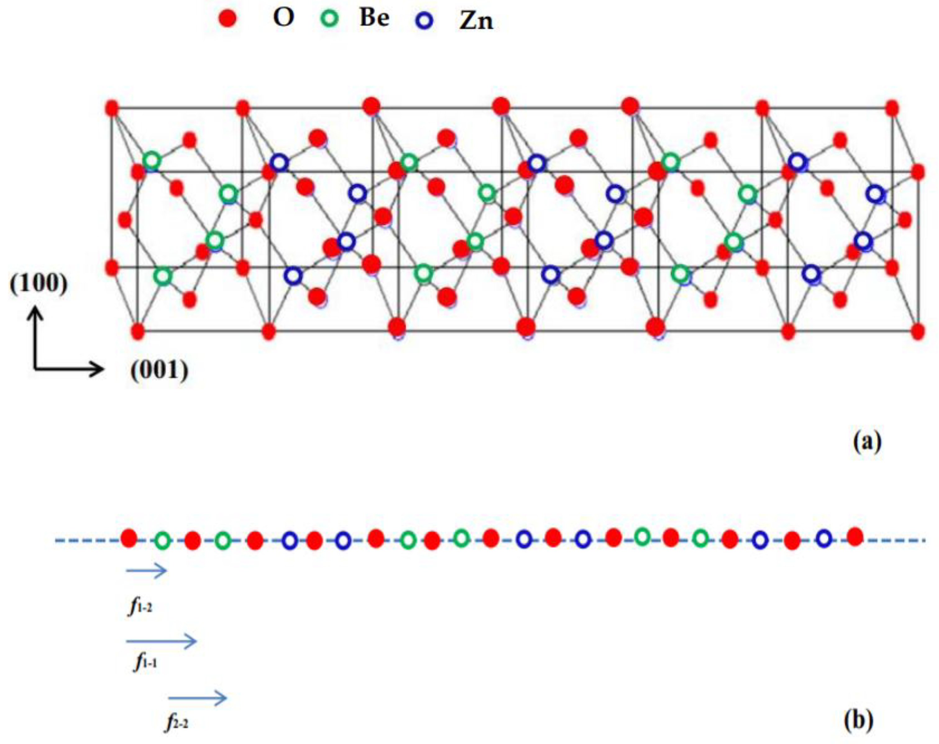
Figure 2.
(a) Calculated longitudinal FAMs of zb (BeO)n/(ZnO)m (0 0 1) SL with dBeO = dZnO (n = m = 10) using Rytov’s ECM model [] with parameters from Table 1. The dotted line represents the phonon wavevector || yielding doublets that can be observed in high-resolution Raman scattering spectroscopy. (b) Calculated frequencies of the first two doublets, as a function of SL period n = m.
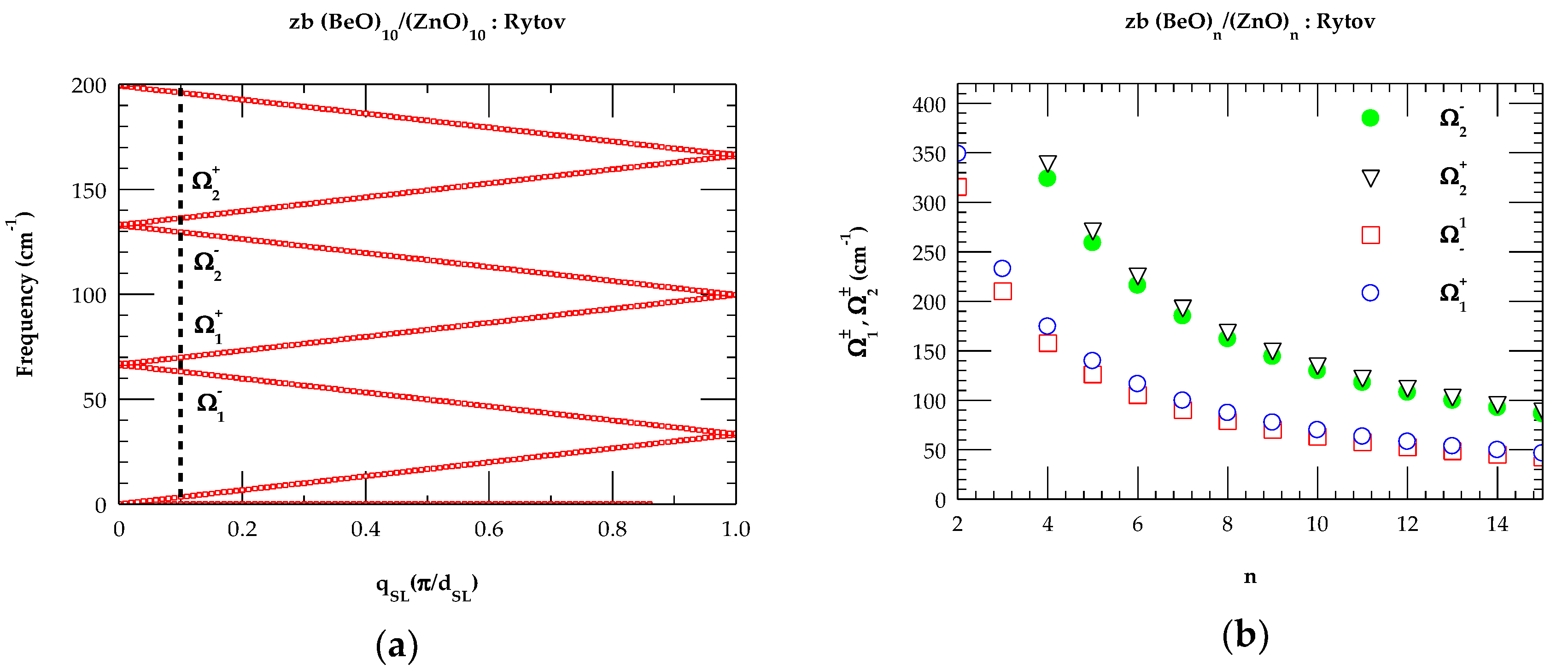
Figure 3.
Calculated MLCM phonon dispersion curves of acoustic modes (Figure 3ab)) and optical phonon branches (Figure 3cd)) for graded (BeO)10-Δ/(BeO0.5ZnO0.5)Δ/(ZnO)10-Δ/(BeO0.5ZnO0.5)Δ SLs.
Figure 3.
Calculated MLCM phonon dispersion curves of acoustic modes (Figure 3ab)) and optical phonon branches (Figure 3cd)) for graded (BeO)10-Δ/(BeO0.5ZnO0.5)Δ/(ZnO)10-Δ/(BeO0.5ZnO0.5)Δ SLs.
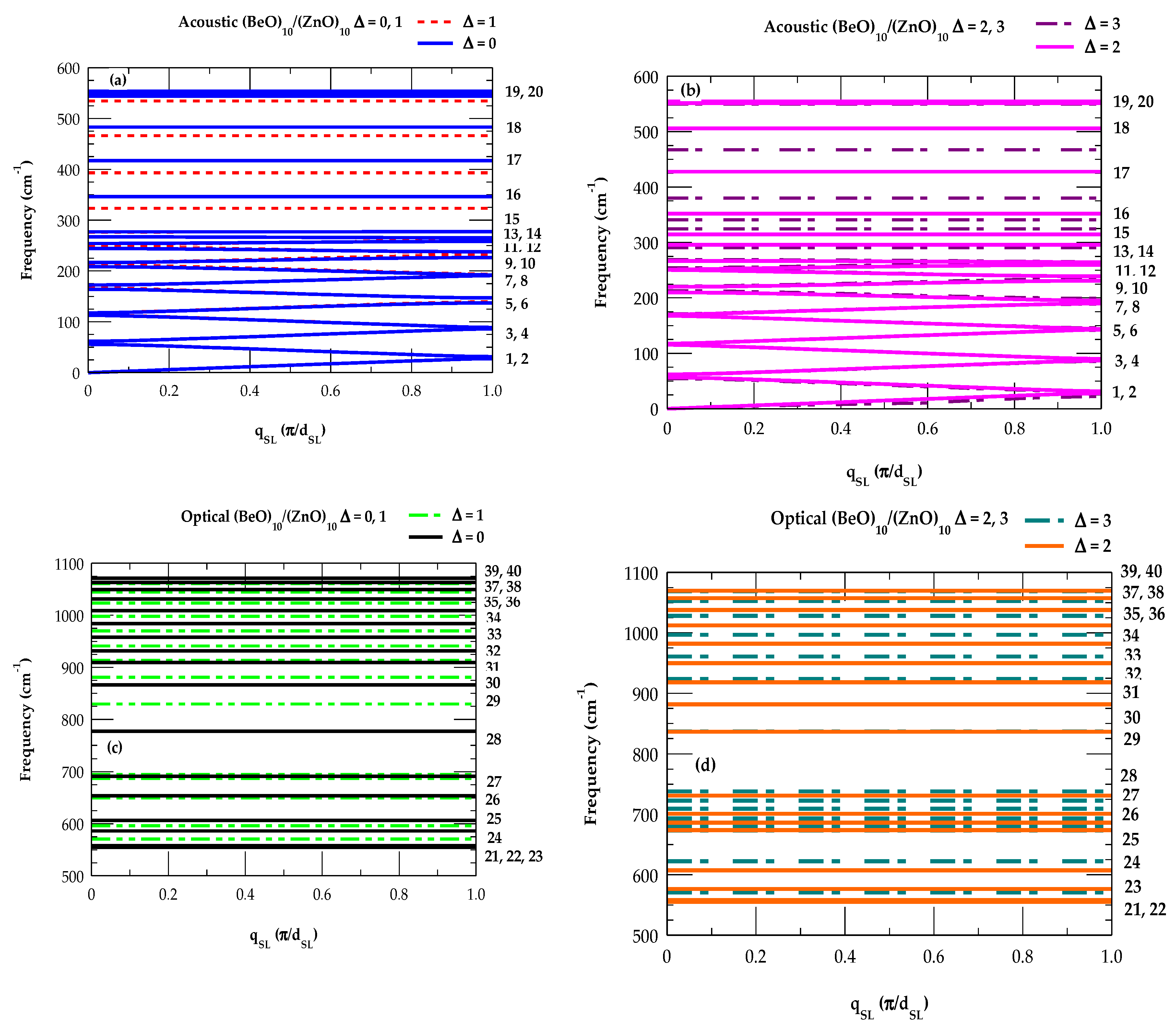
Figure 4.
Simulated Raman scattering spectra based on bond-polarizability model of the confined optical modes for graded (BeO)10-Δ/(Be0.5ZnO0.5O)Δ/(ZnO)10-Δ/(Be0.5ZnO0.5O)Δ SLs for different, interfacial thickness Δ = 0, 1, 2, 3 MLs.
Figure 4.
Simulated Raman scattering spectra based on bond-polarizability model of the confined optical modes for graded (BeO)10-Δ/(Be0.5ZnO0.5O)Δ/(ZnO)10-Δ/(Be0.5ZnO0.5O)Δ SLs for different, interfacial thickness Δ = 0, 1, 2, 3 MLs.
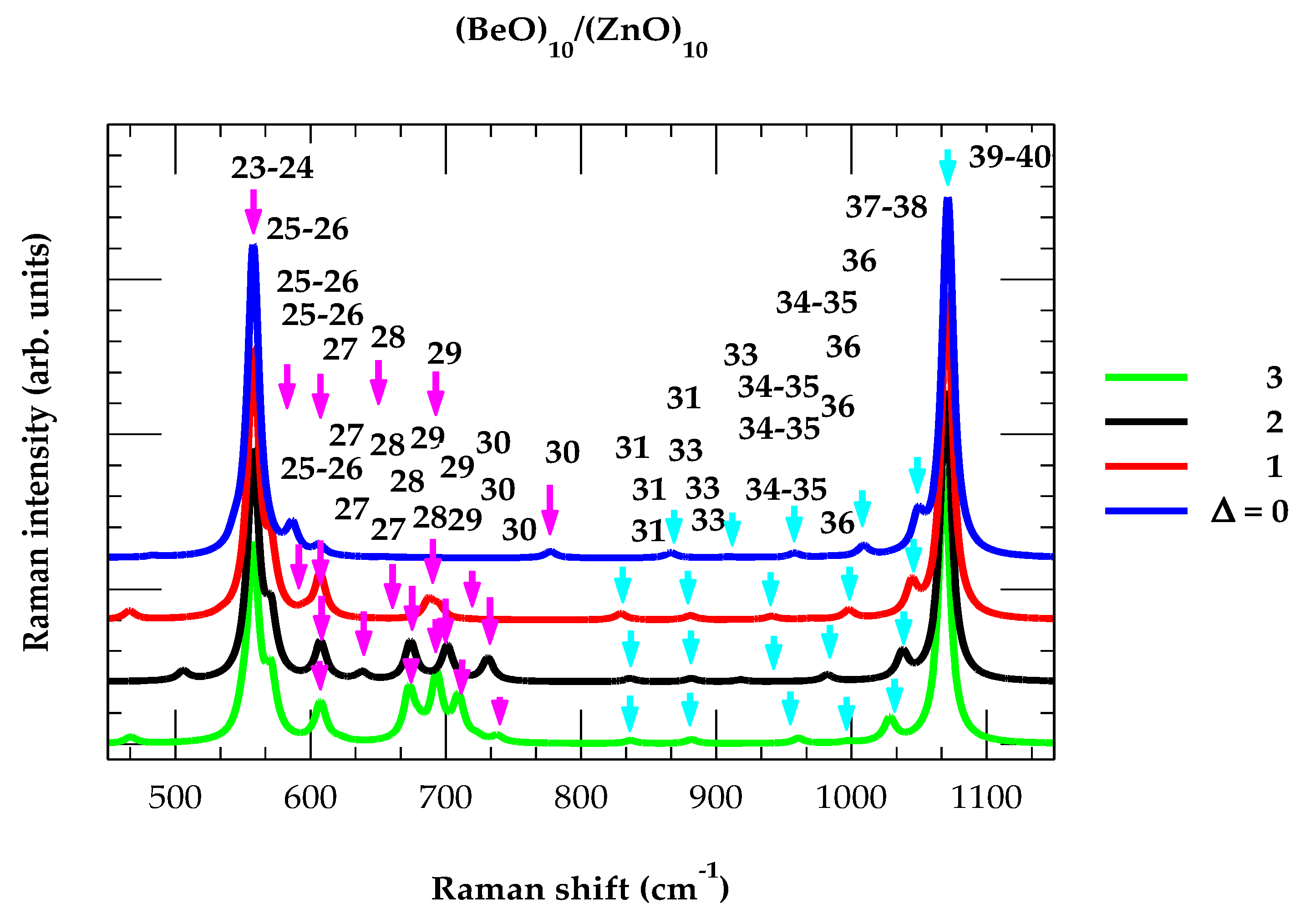
Figure 5.
Impact of the layer thickness (m = n =10; with Δ = 0) on simulated Raman scattering spectra of confined optical modes in graded (BeO)10-Δ/(Be0.5ZnO0.5O)Δ/(ZnO)10-Δ/(Be0.5ZnO0.5O)Δ SLs.
Figure 5.
Impact of the layer thickness (m = n =10; with Δ = 0) on simulated Raman scattering spectra of confined optical modes in graded (BeO)10-Δ/(Be0.5ZnO0.5O)Δ/(ZnO)10-Δ/(Be0.5ZnO0.5O)Δ SLs.
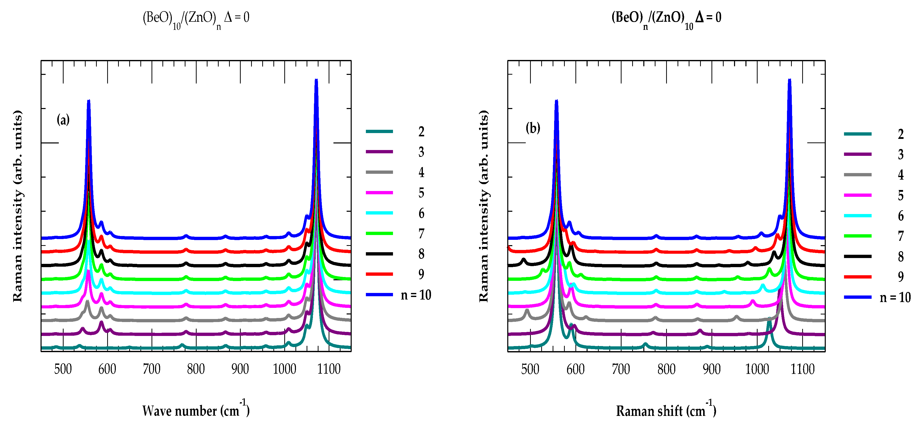
Figure 6.
Impact of the layer thickness (m = n =10; with Δ = 1 ML) on simulated Raman scattering spectra of confined optical modes in graded (BeO)10-Δ/(Be0.5ZnO0.5O)Δ/(ZnO)10-Δ/(Be0.5ZnO0.5O)Δ SLs.
Figure 6.
Impact of the layer thickness (m = n =10; with Δ = 1 ML) on simulated Raman scattering spectra of confined optical modes in graded (BeO)10-Δ/(Be0.5ZnO0.5O)Δ/(ZnO)10-Δ/(Be0.5ZnO0.5O)Δ SLs.
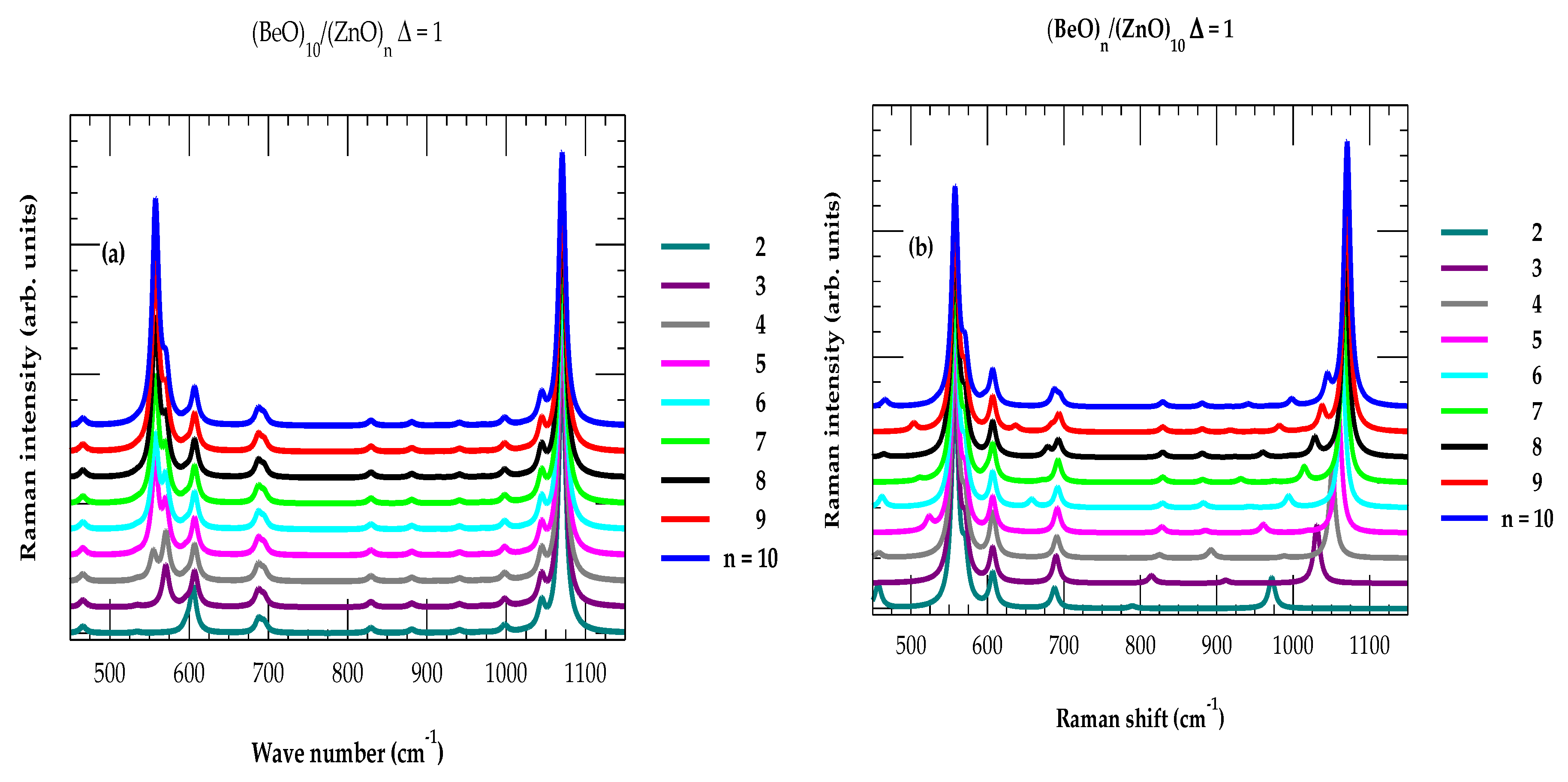
Figure 7.
Impact of the layer thickness (m = n =10; with Δ = 2 ML) on simulated Raman scattering spectra of confined optical modes in graded (BeO)10-Δ/(Be0.5ZnO0.5O)Δ/(ZnO)10-Δ/(Be0.5ZnO0.5O)Δ SLs.
Figure 7.
Impact of the layer thickness (m = n =10; with Δ = 2 ML) on simulated Raman scattering spectra of confined optical modes in graded (BeO)10-Δ/(Be0.5ZnO0.5O)Δ/(ZnO)10-Δ/(Be0.5ZnO0.5O)Δ SLs.
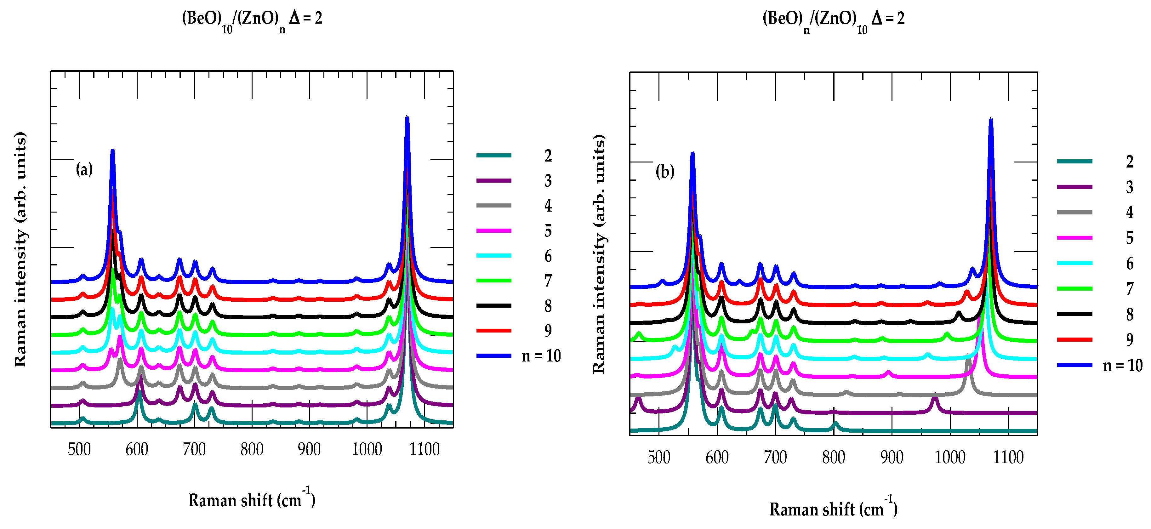
Figure 8.
Impact of the layer thickness (m = n =10; with Δ = 3 ML) on simulated Raman scattering spectra of confined optical modes in graded (BeO)10-Δ/(Be0.5ZnO0.5O)Δ/(ZnO)10-Δ/(Be0.5ZnO0.5O)Δ SLs.
Figure 8.
Impact of the layer thickness (m = n =10; with Δ = 3 ML) on simulated Raman scattering spectra of confined optical modes in graded (BeO)10-Δ/(Be0.5ZnO0.5O)Δ/(ZnO)10-Δ/(Be0.5ZnO0.5O)Δ SLs.
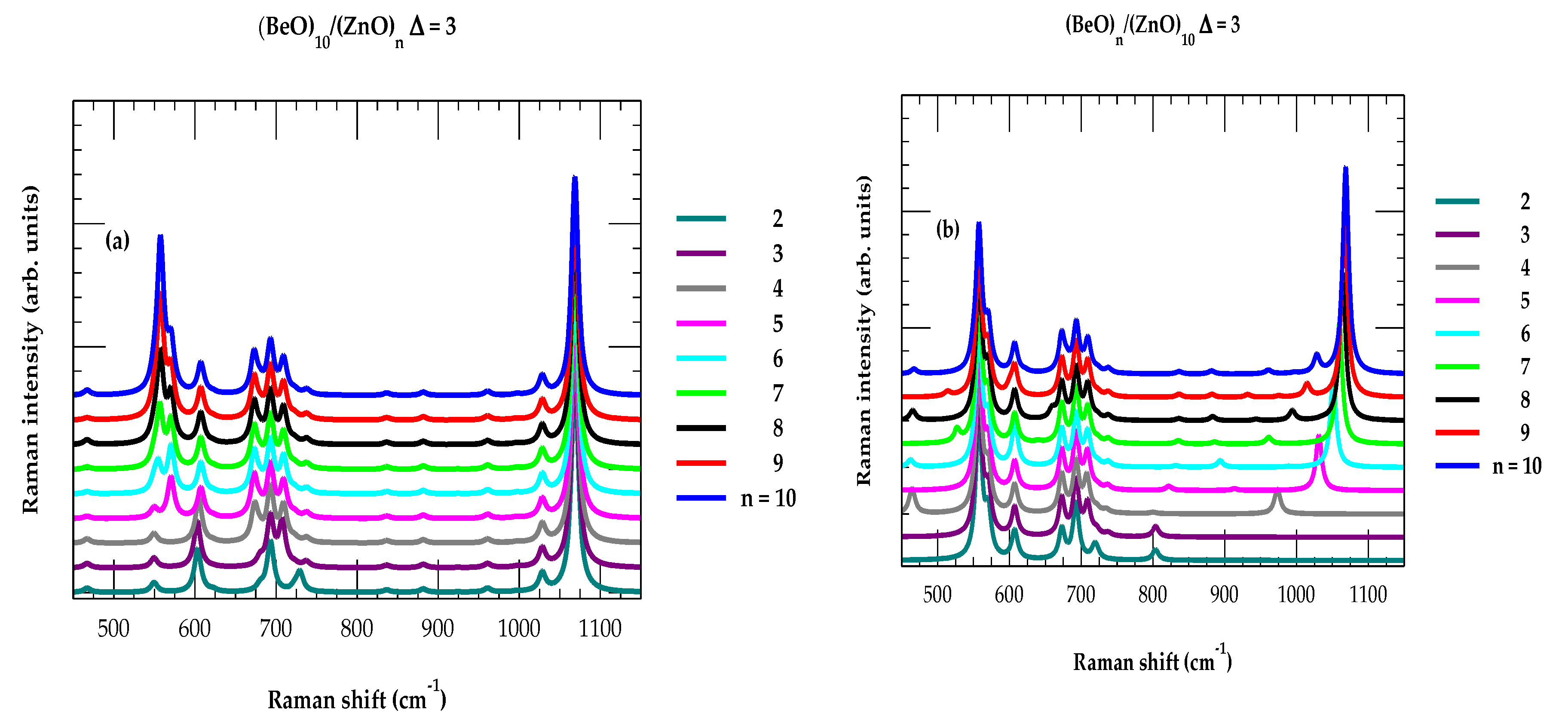
Figure 9.
(a) Calculated frequency shifts versus interface thickness Δ (= 0, 1, 2, 3 MLs) for the COMs 21-30, and (b) 31-40 in the graded (BeO)10-Δ/(Be0.5ZnO0.5O)Δ/(ZnO)10-Δ/(Be0.5ZnO0.5O)Δ SLs (see text).
Figure 9.
(a) Calculated frequency shifts versus interface thickness Δ (= 0, 1, 2, 3 MLs) for the COMs 21-30, and (b) 31-40 in the graded (BeO)10-Δ/(Be0.5ZnO0.5O)Δ/(ZnO)10-Δ/(Be0.5ZnO0.5O)Δ SLs (see text).
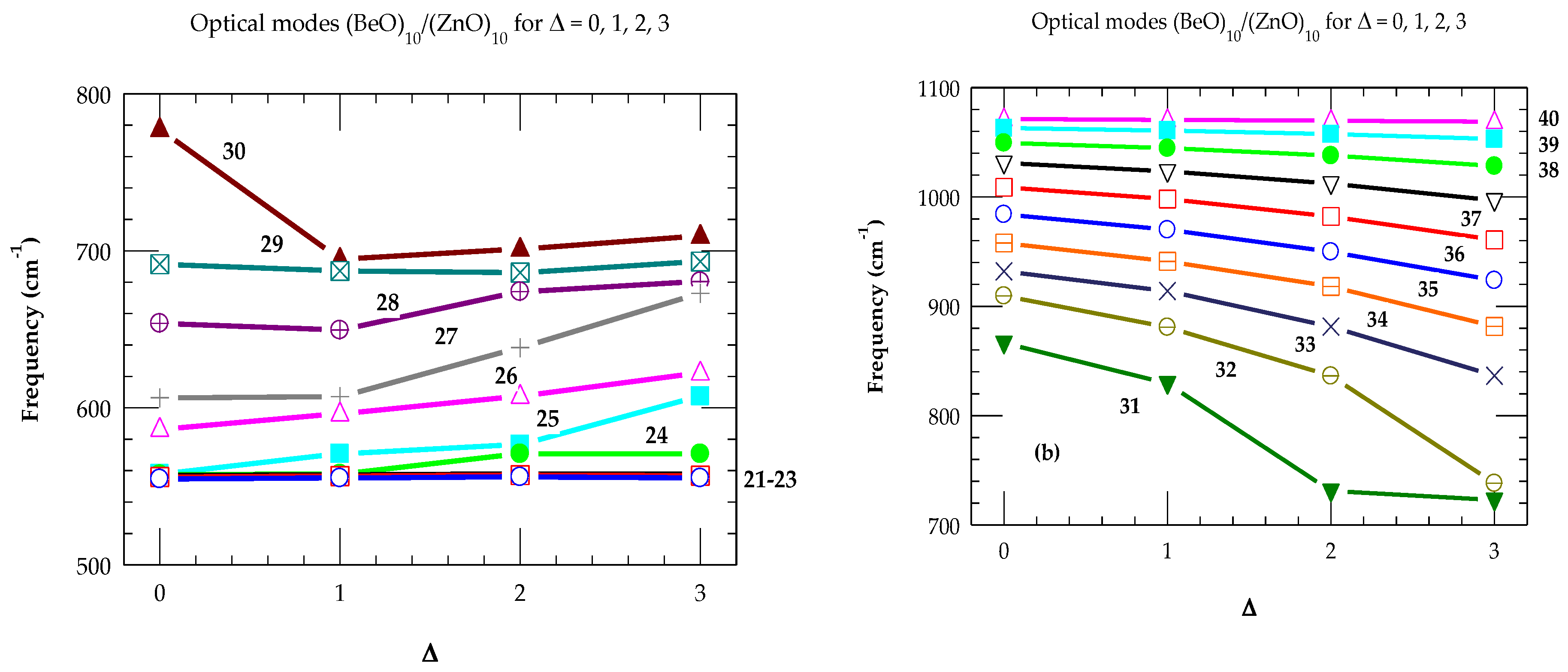
Figure 10.
Atomic displacements as a function of Δ = 0, 1, 2, 3, for some selected optical modes of (BeO)10-Δ/(Be0.5ZnO0.5O)Δ/(ZnO)10-Δ/(Be0.5ZnO0.5O)Δ SLs. Red, blue and green colored filled circles represent, respectively the Be, O and Zn atoms.
Figure 10.
Atomic displacements as a function of Δ = 0, 1, 2, 3, for some selected optical modes of (BeO)10-Δ/(Be0.5ZnO0.5O)Δ/(ZnO)10-Δ/(Be0.5ZnO0.5O)Δ SLs. Red, blue and green colored filled circles represent, respectively the Be, O and Zn atoms.
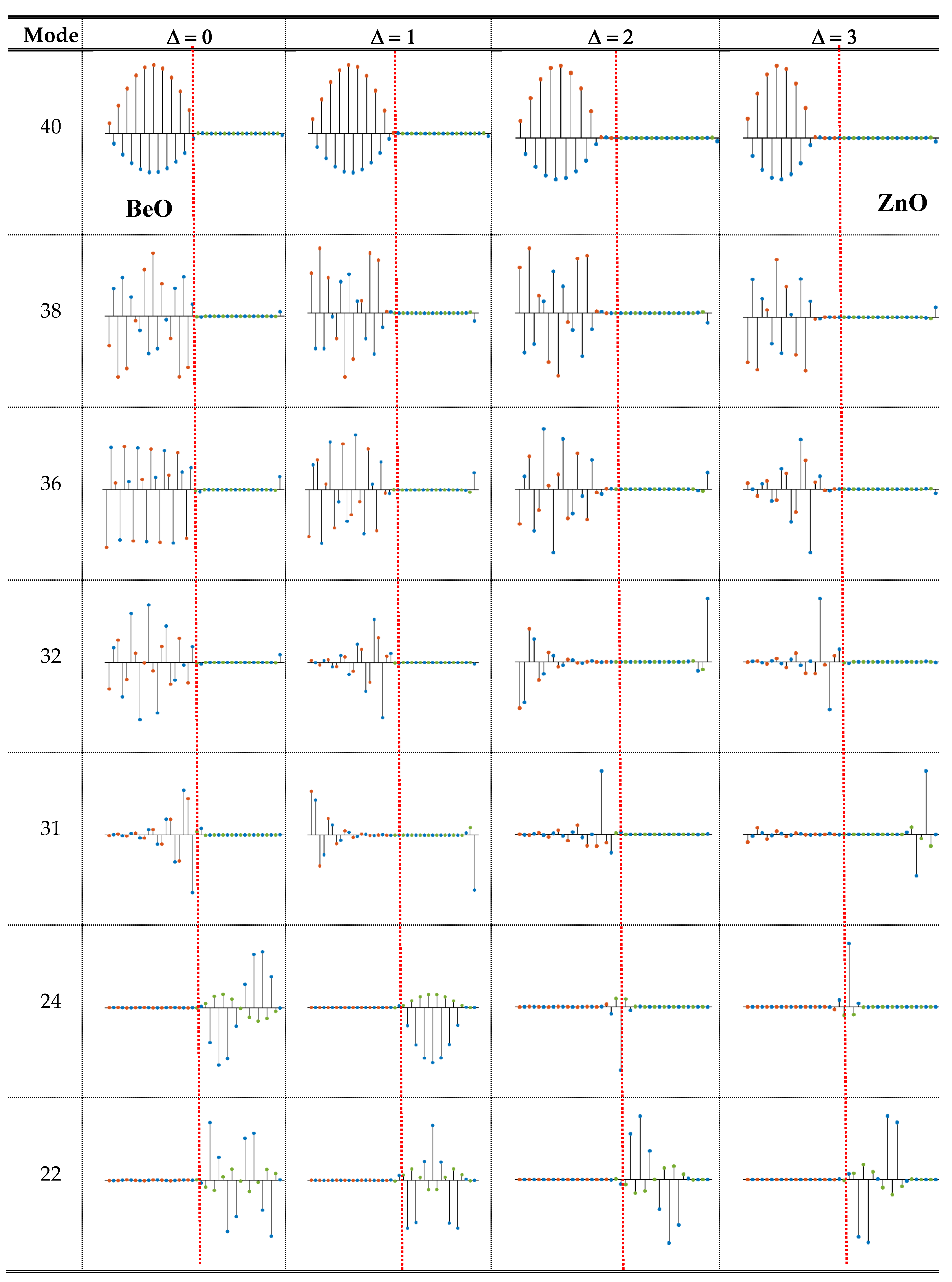

Table 1.
Basic parameters (e.g., lattice constant, elastic constant, mass density, sound velocity and critical point phonons) of the bulk zb BeO and zb ZnO used in the calculations of FAPs; MLCM phonon dispersions; and Raman intensity profiles in zb BeO/ZnO SLs.
Table 1.
Basic parameters (e.g., lattice constant, elastic constant, mass density, sound velocity and critical point phonons) of the bulk zb BeO and zb ZnO used in the calculations of FAPs; MLCM phonon dispersions; and Raman intensity profiles in zb BeO/ZnO SLs.
| Parameters | zb BeO | zb ZnO |
| 3.80 | 4.50 | |
| (1011dyn cm-2) | 34.2 | 19.19 |
| (g cm-3) | 3.0287 | 5.9339 |
| (105 cm s-1) | 10.626 | 5.6883 |
| (cm-1) | 1071 | 558 |
| (cm-1) | 899 | 551 |
| (cm-1) | 707 | 269 |
Table 2.
Selected simulated confined optical phonon frequencies ω0 at Δ = 0 for the (BeO)10/(ZnO)10 SL. The shift in frequencies Δω10, Δω20, Δω30 is also listed by varying interfacial thickness Δ = 1, 2, 3 ML. All phonon values reported near || = 0 are in wavenumbers (cm-1).
Table 2.
Selected simulated confined optical phonon frequencies ω0 at Δ = 0 for the (BeO)10/(ZnO)10 SL. The shift in frequencies Δω10, Δω20, Δω30 is also listed by varying interfacial thickness Δ = 1, 2, 3 ML. All phonon values reported near || = 0 are in wavenumbers (cm-1).
| N | ω0 | Δω10 | Δω20 | Δω30 |
| 21 | 554.7 | 0.6 | 1.3 | 0.6 |
| 25 | 586.4 | 9.8 | 21.0 | 35.9 |
| 26 | 606.4 | 0.7 | 31.9 | 66.6 |
| 27 | 653.8 | -4.3 | 20.2 | 26.6 |
| 29 | 691.5 | -4.3 | -5.4 | 1.7 |
| 30 | 777.4 | -79.7 | -76.3 | -69.0 |
| 31 | 866.4 | -37.0 | -135.3 | -143.5 |
| 32 | 909.5 | -28.5 | -73.1 | -171.4 |
| 33 | 932 | -18.1 | -50.6 | -95.5 |
| 34 | 957.9 | -16.8 | -39.8 | -76.3 |
| 35 | 984.1 | -14.0 | -34.3 | -60.3 |
| 36 | 1008.9 | -10.8 | -26.7 | -48.1 |
| 37 | 1031.1 | -7.7 | -18.9 | -34.3 |
| 38 | 1049.4 | -4.8 | -11.6 | -21.0 |
| 40 | 1071.2 | -0.6 | -1.4 | -2.5 |
Disclaimer/Publisher’s Note: The statements, opinions and data contained in all publications are solely those of the individual author(s) and contributor(s) and not of MDPI and/or the editor(s). MDPI and/or the editor(s) disclaim responsibility for any injury to people or property resulting from any ideas, methods, instructions or products referred to in the content. |
© 2025 by the authors. Licensee MDPI, Basel, Switzerland. This article is an open access article distributed under the terms and conditions of the Creative Commons Attribution (CC BY) license (http://creativecommons.org/licenses/by/4.0/).
Copyright: This open access article is published under a Creative Commons CC BY 4.0 license, which permit the free download, distribution, and reuse, provided that the author and preprint are cited in any reuse.


