
Submitted:
22 May 2025
Posted:
23 May 2025
You are already at the latest version
Abstract
We theoretically investigate electron–surface optical phonon (SOP) interactions mediated by long-range Fröhlich coupling in monolayer platinum diselenide (PtSe₂) and platinum disulfide (PtS₂) supported on SiO₂ and hexagonal boron nitride (hBN) substrates. Using an effective Hamiltonian approach near the K₊ and K₋ valleys of the hexagonal Brillouin zone, we analyze electronic energy renormalization, polaronic oscillator strength, and SOP-induced scattering rates. Our findings reveal a strong dependence of the interaction strength on the dielectric properties of the substrate, with higher optical phonon energies and larger static permittivities leading to reduced carrier scattering. Moreover, increasing the van der Waals interfacial spacing significantly suppresses scattering due to the exponential decay of the electric field, thereby enhancing carrier mobility and optical performance. These insights underscore the importance of substrate selection and interface engineering as key strategies for tailoring electron–phonon interactions in 2D optoelectronic devices.
Keywords:
Pt‐based van der Waals heterostructures
; polaron
; surface optical phonon
; polaronic oscillator strength
; polaronic scattering rate
; platinum diselenide (PtSe₂)
; platinum disulfide (PtS₂)
1. Introduction
Group-X transition metal dichalcogenides (TMDCs), with the general formula MX2 (where M = Pt or Pd, and X = S, Se, or Te), have garnered considerable attention due to their tunable bandgaps, which range from the visible spectrum in monolayers to the mid-infrared in multilayer forms [1]. These materials also exhibit high electron mobility [2] and exceptional chemical stability under ambient and aqueous conditions [3,4], making them ideal candidates for a wide range of optoelectronic applications. Their unique properties have enabled progress in technologies such as broadband photodetectors [5], light-emitting devices [6], field-effect transistors [7], label-free biosensors [4,8], holographic systems [9], and nanoscale optical components like ultrathin lenses [10]. A thorough understanding of their optical properties is therefore essential for optimizing their integration in advanced device architectures.
Among these TMDCs, platinum diselenide (PtSe2) and platinum disulfide (PtS2) stand out for their versatile electronic and optical behavior. PtSe2 displays a thickness-dependent band structure, transitioning from a semiconducting monolayer to a semimetallic bulk phase. This feature enables precise tuning of its conductivity and bandgap, making it suitable for nanoelectronic applications. Furthermore, its high electron mobility and strong spin–orbit coupling make it a promising material for logic circuits, photodetectors, and spintronic devices [11]. In contrast, PtS2 retains semiconducting behavior even in multilayer configurations, with a notable indirect bandgap and high photoresponsivity under visible light [12]. Both materials exhibit excellent ambient stability, which is critical for practical deployment. Optically, PtSe2 and PtS2 demonstrate strong light–matter interactions, high absorption coefficients across the visible to near-infrared range, and fast photoresponse times, rendering them attractive for broadband photodetection, optical modulation, and flexible sensing applications [13,14]. Additionally, their compatibility with layered heterostructures enables fine-tuning of optical responses through interlayer coupling and dielectric engineering.
The role of dielectric substrates, particularly polar materials such as silicon dioxide (SiO2) and hexagonal boron nitride (hBN), is pivotal in the fabrication of van der Waals heterostructures involving PtSe2 and PtS2. SiO2, widely used in microelectronics as a gate dielectric, has a relatively low dielectric constant (~3.9), a wide bandgap (~9 eV), and supports surface optical (SO) phonon modes that can interact with charge carriers in adjacent 2D layers. This interaction, particularly via the long-range Fröhlich mechanism, can significantly influence carrier mobility, scattering processes, and the optical response of the TMDC layers, especially under high electric fields or elevated temperatures [15,16]. In contrast, hBN provides an atomically flat, chemically inert surface with high thermal conductivity and a wide bandgap (~6 eV). Its low defect density helps preserve the intrinsic properties of TMDC monolayers, while reducing charge in homogeneities and suppressing non-radiative recombination [17,18]. Understanding and tailoring the interaction between substrate phonons and 2D materials is therefore critical for enhancing charge transport and optical performance in TMDC-based heterostructures.
When integrated with insulating substrates such as SiO2 and hBN, platinum-based TMDCs can form heterostructures with enhanced performance. PtSe2/SiO2 systems, for example, exhibit high carrier mobility and thickness-dependent bandgap transitions, enabling efficient photodetection across the visible to infrared range [19]. Similarly, PtS2 films grown on SiO2 maintain stable semiconducting behavior and structural uniformity, making them suitable for field-effect transistors and optoelectronic devices [12]. On the other hand, the use of hBN as a substrate offers considerable advantages due to its atomically smooth surface, wide bandgap, and chemical inertness. PtSe2/hBN and PtS2/hBN heterostructures preserve the intrinsic properties of the active TMDC layers while minimizing substrate-induced disorder and charge trapping effects [20,21]. These combinations result in improved electrical stability, enhanced optical performance, and low-noise operation, which are crucial for applications in flexible electronics, photodetectors, and spintronic devices.
Recent experimental and theoretical studies have shed light on the structural and functional characteristics of PtSe2 and PtS2 on dielectric substrates such as SiO2 and hBN. Ullah et al., demonstrated the fabrication of high-performance PtSe2/SiO2 photodetectors with broadband sensitivity and ultrafast response, attributed to the high carrier mobility and tunable band structure of the PtSe2 layer [19]. In parallel, Aftab et al., reported on the deposition of environmentally stable PtS2 thin films on SiO2, highlighting their uniform morphology and sustained semiconducting nature, which are essential for integration into optoelectronic and FET devices [12].
On the hBN side, Jia et al., achieved epitaxial growth of PtSe2 on hBN using molecular beam epitaxy, demonstrating enhanced photodetector performance and reduced defect scattering due to the flat and inert nature of the substrate [20]. Kim et al., also investigated charge transport in PtS2/hBN heterostructures and observed low-noise performance and efficient carrier mobility, critical attributes for next-generation low-power and flexible devices [21]. These combined efforts underscore the synergy between experimental and theoretical approaches in the design and optimization of Pt-based van der Waals heterostructures for advanced optoelectronic, sensing, and spintronic applications.
This study presents a detailed theoretical investigation of electron–surface optical phonon (SOP) interactions in monolayer platinum disulfide (PtS2) and platinum diselenide (PtSe2) deposited on polar dielectric substrates, namely silicon dioxide (SiO2) and hexagonal boron nitride (hBN). These interactions play a critical role in shaping the electronic and optical behavior of two-dimensional (2D) materials integrated into heterostructures. Our study begins with an analysis of the substrate-induced electron–phonon coupling mechanisms, followed by a quantitative evaluation of the resulting polaronic oscillator strength. This allows us to assess the extent to which the dielectric environment modifies the optical response of the monolayers. We further examine the temperature dependence of the polaronic scattering rate to elucidate the impact of thermal fluctuations on carrier dynamics. In addition, we analyze how the van der Waals (vdW) separation between the monolayer and the substrate influences SOP-mediated scattering, offering deeper insight into the interplay between interfacial geometry and many-body effects in 2D material systems.
2. Electron-Surface Optical Phonon Interaction in ML PtSe2 and PtS2 on Polar Substrates
Monolayer PtS2 and PtSe2 are part of the group-10 transition metal dichalcogenides and adopt a 1T-phase structure, where a central layer of platinum (Pt) atoms is sandwiched between two layers of chalcogen atoms—either sulfur (S) or selenium (Se). These atoms form a hexagonal lattice in which the Pt atoms are arranged in a two-dimensional triangular Bravais lattice, with the chalcogen atoms occupying aligned positions above and below the Pt plane. The real-space lattice is defined by the primitive vectors and , where is the lattice constant (see Figure 1. (a)). In reciprocal space, the structure is also triangular, with reciprocal lattice and (see Figure 1. (b)). The first Brillouin zone is hexagonal and contains high-symmetry points such as Γ at the center, K+ and K− at the corners, and M at the midpoints of the edges. These points play a crucial role in determining the electronic, optical, and vibrational properties of PtS2 and PtSe2, particularly in the context of band structure and excitonic phenomena.
The corresponding reciprocal lattice also forms a hexagonal structure, with the first Brillouin zone exhibiting high-symmetry points labeled Γ, K, and M. These points play a crucial role in the electronic band structure. These points are critical for understanding the electronic band dispersion and optical transitions, particularly in the context of interband transitions and electron–phonon interactions. Notably, unlike other TMDCs such as MoS2, PtSe2 and PtS2 exhibit an indirect band gap in their monolayer form, with the valence band maximum located at the Γ point and the conduction band minimum near the M point. This distinct band alignment influences their optical and transport properties, making them suitable for specific optoelectronic and sensing applications. The high-symmetry points denoted as are defined as follows:
Near the K+ point, the behavior of the conduction and valence band states with parallel spin can be described using an effective 2×2 Hamiltonian, expressed as follows [22,23,24]:
Here, represents the in-plane wave vector measured relative to the point. The parameter is proportional to the square of the interband momentum matrix element and is given by where denotes the effective mass of the electron, and corresponds to the band gap energy.
For spin sublevels with in the same valley, the Hamiltonian retains the structure of Equation (1), but with the band gap replaced by , where accounts for the combined spin–orbit splitting of the conduction and valence bands. In the valley, the corresponding effective Hamiltonian is obtained from Equation (1) by replacing with .
The energy dispersion relation obtained from the Hamiltonian in Equation (1) exhibits a Dirac-like form:
In this context, and refer to the conduction and valence bands, respectively. For the sake of computational feasibility, our study assumes idealized conditions with uniform, defect-free interfaces between the PtSe2 and PtS2 monolayers and the underlying dielectric substrates, an approximation commonly adopted in theoretical modeling and simulation.
In this study, we investigate the interaction between electrons and surface optical phonons (SOPs) in monolayer (ML) PtSe2 and PtS2 supported on SiO2 and hexagonal boron nitride (hBN) substrates, within the framework of long-range Fröhlich coupling. This model provides a solid theoretical foundation for describing electron–SOP interactions in these 2D materials on polar substrates. However, it involves several simplifying assumptions. For instance, it relies on the Born–Oppenheimer approximation [25] and neglects short-range electron–phonon interactions, which may play a role in non-polar environments [26]. The model also assumes a constant effective electron mass, and typically disregards non-linear effects and multi-phonon processes [27]. Furthermore, it does not account for the presence of impurities, defects, or other sources of disorder [25,28]. Phonon dispersion is often approximated as linear, which may not be valid across all phonon branches or substrate types [29]. Finally, the analysis usually focuses on a single dominant phonon mode, potentially overlooking contributions from other relevant modes.
For simplicity, the phonon spectrum is treated as isotropic, allowing us to classify phonons as either longitudinal or transverse. The electron–phonon interaction described by the Fröhlich Hamiltonian involves a scattering event in which an electron transitions from an initial momentum state to a final state , due to the emission or absorption of a phonon. In both processes, the conservation of total momentum holds and can be written as:
The term represents the phonon energy contribution, accounting for both longitudinal optical (LO) and surface optical (SO) phonon modes, and is given by:
In this expression, , , denote the creation and annihilation operators, respectively, for a phonon with wave vector , while represents the phonon frequency associated with mode . The second term, , describes the electron–phonon interaction Hamiltonian [30]:
The Fröhlich Hamiltonian, which describes the long-range interaction between electrons and polar optical phonons, is given by:
The interaction between charge carriers in monolayer PtSe2 and PtS2 and the surface optical phonons is described by the second term in Equation (6). The coupling matrix element in the Fröhlich Hamiltonian quantifies the strength of the interaction between an electron in the monolayer and a surface optical phonon mode of the polar substrate. It is given by the following expression [31,32,33]:
In this context, denotes the strength of the polarization field associated with phonon mode and is determined by the Fröhlich coupling constant [34]:
Here, and are the static (low-frequency) and high-frequency dielectric constants of the polar substrate, respectively (see Table 1). The parameter represents the vertical separation between the monolayer PtSe2 and PtS2 and the polar substrate (see Table 2). The quantity corresponds to the energy of the surface optical (SO) phonons, with denoting the two phonon branches.
The surface optical phonon (SOP) energies are derived from the bulk longitudinal optical (LO) phonon modes using the following relation [30]:
The screening of the Coulomb interaction by the surrounding polar dielectric environment is accounted for using the parameter . Due to the weak screening of the out-of-plane electric field in monolayer PtSe2 and PtS2, is taken to be 1 [43].
On polar substrates, surface optical phonons (SOPs) generate an electric field that interacts with electrons in the adjacent monolayer PtSe2 and PtS2. Based on equations (7) and (8), the SOP coupling strength can be expressed as:
The summation is carried out over a single spin orientation and a single valley. Here, represents the area of the two-atom unit cell, with being the lattice constant.
In this work, we adopt the same theoretical approach as outlined in our previous studies [44,45,46,47,48,49,50,51,52]. To investigate the interaction between electrons and surface optical phonons in monolayer PtSe2 and PtS2, we focus on the electronic states and , associated with electron energies and , respectively. Additionally, we consider an effective 2×2 Hamiltonian that describes the conduction and valence band states with parallel spin projections , in the vicinity of the point of the hexagonal Brillouin zone.
The space of polaronic states arises from the tensor product of the electronic and phononic state subspaces. Consequently, we define new states, referred to as polaronic states, given by:
The polaronic electron energies for the states in monolayer PtSe2 and PtS2, on polar substrates are expressed as follows [44,45,46,47,48,49,50,51,52]:
Figure 2 illustrates the strength of the surface optical (SO) coupling between the electronic states ⟩ and as a function of the wave vector in monolayer PtS2 on SiO2 and hBN polar substrates. As shown in Figure 2, it is clear that the coupling with surface optical phonons is strongly dependent on the type of polar substrate.
Figure 3 illustrates the polaronic electron energy dispersion as a function of the wave vector for monolayer (ML) PtS2 and PtSe2 deposited on polar substrates, specifically SiO2 and hBN. For reference, the corresponding non-interacting electronic states and are plotted alongside the interacting dispersion. In the case of PtS2, the non-interacting energy branches intersect near on SiO2 and on hBN, indicative of a resonant condition where the energy spacing between the electronic states coincides with the optical phonon energy , which equals for SiO2 and for hBN. These resonances lead to the emergence of pronounced anticrossings in the interacting spectrum, replacing the bare-level crossings and evidencing strong electron–phonon coupling. The resulting Rabi splittings reach approximately on SiO2 and on hBN.
A similar behavior is observed for PtSe2: the non-interacting states intersect around on SiO2 and on hBN. Again, the condition for resonant coupling is met, with energy separations matching the corresponding phonon energies. The strong coupling regime manifests as anticrossings, with Rabi splittings of about and for SiO2 and hBN, respectively. As highlighted in Figure 3, the magnitude of the Rabi splitting is notably larger on hBN compared to SiO2, underscoring an enhancement of the electron–phonon interaction strength in the hBN-supported configurations.
In polar substrates, surface optical (SO) phonons generate electric fields that penetrate into the adjacent monolayer, where they couple directly with electrons in PtSe2 and PtS2, layers via dipole interactions. This coupling significantly enhances the electron–phonon interaction strength, leading to a renormalization of the electronic states. As a result, the energy splitting between hybridized polaronic states increases, manifesting as an enhanced Rabi splitting.
The observed variation in Rabi splitting between silicon dioxide (SiO2) and hexagonal boron nitride (hBN) substrates (Figure 3) arises from the distinct surface phonon characteristics, dielectric properties, and phonon energy scales of the two materials. hBN, for example, exhibits a higher static dielectric constant compared to SiO2, which leads to stronger electric fields associated with its surface phonons at the interface. This results in a more pronounced coupling with monolayer PtSe2 and PtS2, electronic states, thereby amplifying the strength of the electron–phonon interaction and yielding a larger Rabi splitting.
Conversely, SiO2, due to its relatively lower dielectric constant, generates weaker electric fields associated with its surface optical phonons. As a result, the electron–phonon coupling with the PtSe2- and PtS2-monolayer is comparatively weaker, leading to a reduced Rabi splitting. This comparison highlights the crucial influence of the polar substrate in modulating the electron–phonon interaction strength, and consequently, in tuning the optical response and performance of monolayer PtSe2- and PtS2-based optoelectronic devices.
At the anticrossing points, the electronic wave functions become hybridized, enabling multiple transition pathways such as: , and . This behavior indicates that the interaction between electrons and surface optical phonons (SOPs) cannot be treated within the weak-coupling regime. Instead, the strong coupling gives rise to Rabi splitting of the electronic levels. Theoretical calculations thus support the occurrence of energetically resonant coupling between electronic subbands and surface vibrational modes in monolayer TMDCs interfaced with the considered polar substrates. The resulting hybrid states, or polarons, can be expressed as:
The weight of the electronic component and the weight of the one-phonon component of the polaron states ± vary with the polaron energies . The expressions detailing these dependencies are as follows [44,45,46,47,48,49,50,51,52]:
Figure 4 illustrates the variation of the electronic and one-phonon component weights of the lower polaron state in monolayer (ML) PtS2 and PtSe2, supported on SiO2 and hBN polar substrates, as a function of the wave vector . Notably, for ML PtS2 on hBN (refer to Figure 4), the one-phonon component for the lower polaron state becomes dominant near , with its weight significantly exceeding that of the electronic component . This behavior highlights the strong influence of surface optical phonons (SOPs) at the ML PtS2/hBN interface, which facilitate resonant coupling between the non-interacting states and , thereby enabling polaron formation [44,45,46,47,48,49,50,51,52]. Similar trends are observed for the other configurations involving ML PtS2 and PtSe2 on both SiO2 and hBN substrates (refer to Figure 4).
3. Polaronic Oscillator Strength of ML PtS2 and PtSe2 on SiO2 and hBN Dielectric Polar Substrates
In this section, we present a theoretical analysis of the polaronic oscillator strength (OS), a key parameter characterizing light–matter interactions in these systems. Drawing an analogy with interband transitions in quantum dots, we evaluate the OS for interband transitions in ML PtS2 and PtSe2 placed on polar substrates. In the regime of strong confinement, the OS is directly related to the spatial overlap between polaronic states and is expressed in terms of the square modulus of the overlap integral, , as given by the following relation [53,54]:
where denotes the Kane energy, and represents the emission energy associated with a single optical phonon in ML PtS2 and PtSe2 on polar substrates. The latter is given by:
Here, is the energy of the lower polaron branch of the electron, corresponds to the energy of the emitted optical phonon, and denotes the electronic band gap of ML PtS2 and PtSe2. The oscillator strength (OS) has been calculated for the lower polaronic state , which arises as a coherent superposition of the two basis states and :
Figure 5 presents the calculated polaronic oscillator strength (OS) for monolayer PtSe2 on SiO2 and hBN substrates as a function of the wave vector . Our theoretical analysis reveals that the polaronic OS is highly sensitive to the optical phonon modes of the surrounding dielectric environment. This sensitivity arises from the dependence of the phonon emission energy, , on both the material’s band structure and the phonon characteristics of the substrate. Specifically, the emission energy is given by , where is the band gap and is the lower polaron energy. Consequently, the strongest oscillator strength is observed for the substrate with the highest longitudinal optical phonon energy, confirming that .
Using the same approach, it can be readily demonstrated that for monolayer PtS2, the polaronic oscillator strength satisfies the inequality:
This behavior is attributed to the higher dielectric constant of and the greater longitudinal optical (LO) phonon energy compared to that of , (see Table 1). Consequently, the polarization field induced at the ML–substrate interface is stronger for , resulting in a more pronounced polaronic optical response in ML PtS2 and PtSe2 supported on hBN. Furthermore, as shown in Figure 6, the oscillator strength in ML PtSe2 exceeds that in ML PtS2:
This result is explained by the difference in the effective electron masses in the two materials. Heavier electrons, as found in ML PtS2, lead to reduced polaronic oscillator strength near the ML /dielectric interface. In contrast, lighter electrons, such as in ML PtSe2, result in a significant enhancement of the oscillator strength, particularly in the regime of strong confinement.
4. Polaronic Scattering Rate in ML and on Polar Substrates
We now examine the temperature dependence of the polaronic scattering rate induced by surface optical (SO) phonons. The SO phonon scattering rate, which quantifies the rate of momentum relaxation for polarons interacting with interface phonons, is expressed as follows [55]:
Here, denotes the Bose–Einstein occupation number of the phonons, is the angle associated with the direction of the wave vector , and represents the squared modulus of the electron–phonon interaction matrix element, defined as:
The summation symbol ∑ is replaced by the integral , which accounts for integration over the Brillouin zone while incorporating both spin and valley degrees of freedom. Here, denotes the area of the elementary unit cell containing two atoms. Accordingly, the expression transforms into:
Figure 7 illustrates the temperature dependence of the surface optical (SO) phonon scattering rate in monolayer PtSe2 on SiO2 and hBN polar substrates. It is clearly observed that at temperatures above room temperature, the SO phonon scattering rate increases with temperature, reflecting the enhanced phonon population. In contrast, at low temperatures, the scattering rate remains negligible due to the weak phonon occupation. Furthermore, Figure 7 indicates that the scattering rate is consistently higher for the hBN substrate compared to SiO2 across the entire temperature range. This behavior is attributed to the higher LO phonon energy and stronger polarization field associated with the hBN substrate, which enhance electron–phonon interactions at the interface.
Figure 7 further reveals that the surface optical (SO) phonon scattering rate in monolayer PtSe2 is strongly influenced by the dielectric properties of the underlying polar substrate. Specifically, the scattering rate follows the relation:
This behavior arises from the larger dielectric mismatch and stronger polarization fields at the PtSe2/hBN interface, which enhance the Fröhlich-type electron–phonon coupling, thereby increasing the scattering rate.
Ultimately, by selecting an appropriate polar dielectric substrate, it is possible to optimize and enhance the surface optical (SO) phonon scattering rate in monolayer PtSe2 and PtS2, thereby tuning their polaronic and transport properties.
We now explore how the van der Waals (vdW) separation affects the surface optical phonon (SOP) scattering in monolayer PtS2 and PtSe2 with polar substrates, specifically SiO2 and hexagonal boron nitride (hBN) (see Figure 8). At typical interface distances (d = 0.4 nm for SiO2, d = 0.34 nm for hBN as reported in Table 2), strong electron–phonon coupling is observed due to the proximity of the 2D layer to the SOP field. However, as the vdW distance increases to d = 1.0 nm, the SOP-induced scattering rate drops significantly—by more than an order of magnitude—due to the exponential decay of the electric field away from the substrate. This reduction leads to enhanced carrier mobility and improved optoelectronic properties. These results underscore the critical importance of interfacial spacing as a tunable parameter for engineering electron–phonon interactions in two-dimensional materials, with direct implications for next-generation optoelectronic device design.
A thorough understanding of electron–surface optical phonon (SOP) interactions in monolayer PtS2 and PtSe2 necessitates close attention to the dielectric environment—especially when these materials are supported on polar substrates such as SiO2 and hexagonal boron nitride (hBN). The substrate’s dielectric response plays a dual role: it screens Coulomb interactions, thereby modulating excitonic binding energies and carrier mobility, while simultaneously introducing remote surface optical phonon modes that open additional scattering channels. Gopalan et al. [56], through first-principles transport calculations, highlighted this trade-off by showing that although high-κ dielectrics can suppress intrinsic phonon scattering and enhance mobility, the presence of remote interfacial phonons from polar substrates can counteract these gains by reintroducing scattering pathways.
This interplay becomes particularly critical in PtS2 and PtSe2 due to their pronounced polarizability and quasi-flat electronic bands, which amplify sensitivity to substrate-induced perturbations. Experimental observations further corroborate this susceptibility. Chow et al. [57] reported the emergence of symmetry-forbidden Raman modes in TMDC monolayers interfaced with hBN, attributing them to strong exciton–phonon coupling at the van der Waals interface. Similarly, Kizel et al. [58] demonstrated that asymmetric dielectric environments in rhombohedral MoS2 heterostructures induce polarization-dependent shifts in photoluminescence, resulting from exciton–trion rebalancing governed by Fermi level tuning—an effect potentially mirrored in Pt-based dichalcogenides.
These findings align with Giustino’s comprehensive theoretical framework [59], which emphasizes that both short- and long-range dielectric screening profoundly modulate electron–phonon interactions in low-dimensional materials. Complementary insights are provided by Stier et al. [60], who showed that excitonic properties in WSe2 can be finely tuned via substrate engineering, with significant impacts on exciton binding energies and optical spectra.
Recent studies further underscore the importance of interfacial dielectric design. Adeniran and Liu [61] investigated the spatially resolved screening profile at TMDC/hBN interfaces, revealing that screening strength evolves markedly from monolayer to bulk due to local-field effects. Their work underscores the role of interface-specific dielectric engineering in optimizing transport and optical response. Knobloch et al. [62] further confirmed that hBN, thanks to its atomically flat surface and low impurity density, outperforms SiO2 in enabling high-mobility, low-scattering device platforms—an essential requirement for PtS2 and PtSe2 integration. Lastly, Wang et al. [63] demonstrated that substrate selection (e.g., SiO2 vs. hBN) critically impacts carrier polarity and transport efficiency in 2D materials, reinforcing the idea that substrate-driven electron–phonon coupling is a tunable and decisive factor in device performance.
Altogether, these theoretical and experimental advances converge to highlight the critical role of dielectric engineering in governing SOP-mediated processes in PtS2 and PtSe2 monolayers. Substrate choice, especially when involving polar materials like SiO2 and hBN, emerges as a decisive factor for tailoring excitonic phenomena, phonon-assisted scattering, and overall optoelectronic performance in 2D heterostructures.
Furthermore, the interaction with surface optical phonon (SOP) modes leads to the formation of polaronic states, which play a critical role in the energy relaxation processes within PtS2 and PtSe2 monolayers. By adjusting the strength of this coupling—achievable through careful selection of the supporting polar substrate—it becomes possible to influence the dynamics of phonon-assisted hot carrier relaxation. This level of control is particularly advantageous for improving the performance of devices such as photodetectors and solar cells, where efficient energy dissipation and rapid carrier response are essential.
5. Conclusions
In summary, our study highlights the pronounced influence of the polar substrate on the strength of the surface optical phonon (SOP) coupling in monolayer PtSe2 and PtS2. We find that the resonant interaction between electronic sub-levels and surface polar vibrational modes gives rise to a Rabi-like splitting of electronic states, signaling strong light–matter hybridization in these systems. This resonance occurs when the energies of the electronic and vibrational modes become comparable, resulting in a robust coupling mediated by the interfacial polarization field. Such coupling mechanisms are expected to suppress nonradiative recombination channels and thereby improve photoluminescence (PL) efficiency.
Moreover, we show that the most intense interfacial polarization fields lead to the strongest polaronic oscillator strength (OS) and an enhancement in surface optical phonon scattering rates. These polaronic effects—both in oscillator strength and scattering dynamics—are highly sensitive to the dielectric properties of the substrate. The emergence of polaronic states introduces new pathways for carrier energy relaxation, emphasizing their potential role in tuning the optoelectronic performance of monolayer PtSe2 and PtS2. Overall, our findings underscore the critical importance of electron–surface phonon interactions in dictating the carrier dynamics and energy dissipation processes in two-dimensional semiconductors, especially in contexts involving hot carrier relaxation.
We have also explored how the van der Waals (vdW) separation affects the surface optical phonon (SOP) scattering in monolayer PtS2 and PtSe2 with polar substrates, strong electron–phonon coupling is observed due to the proximity of the 2D layer to the SOP field. However, as the vdW distance increases to d = 1.0 nm, the SOP-induced scattering rate drops significantly—by more than an order of magnitude—due to the exponential decay of the electric field away from the substrate. This reduction leads to enhanced carrier mobility and improved optoelectronic properties. These results underscore the critical importance of interfacial spacing as a tunable parameter for engineering electron–phonon interactions in two-dimensional materials, with direct implications for next-generation optoelectronic device design.
Author Contributions
Conceptualization and visualization M.M., R.B., A.O. and S.G.; methodology, M.M.; investigation and formal analysis, M.M.; writing—original draft preparation, M.M.; writing—review and editing, M.M., R.B., and S.G.; supervision, S.G. All authors have read and agreed to the published version of the manuscript.
Funding
This research received no funding.
Institutional Review Board Statement
Not applicable.
Informed Consent Statement
Not applicable.
Data Availability Statement
The data presented in this study are available on request from the corresponding author. The data are not publicly available due to privacy issues.
Conflicts of Interest
The authors declare no conflicts of interest.
References
- Miró, P.; Ghorbani-Asl, M.; Heine, T. Two Dimensional Materials Beyond MoS2: Noble-Transition-Metal Dichalcogenides. Angew. Chemie Int. Ed. 2014, 53, 3015–3018. [Google Scholar] [CrossRef] [PubMed]
- Zhao, Y.; Qiao, J.; Yu, Z.; Yu, P.; Xu, K.; Lau, S.P.; Zhou, W.; Liu, Z.; Wang, X.; Ji, W.; et al. High-Electron-Mobility and Air-Stable 2D Layered PtSe2 FETs. Adv. Mater. 2017, 29, 1604230. [Google Scholar] [CrossRef]
- Oyedele, A.D.; Yang, S.; Liang, L.; Puretzky, A.A.; Wang, K.; Zhang, J.; Yu, P.; Pudasaini, P.R.; Ghosh, A.W.; Liu, Z.; et al. PdSe2: Pentagonal Two-Dimensional Layers with High Air Stability for Electronics. J. Am. Chem. Soc. 2017, 139, 14090–14097. [Google Scholar] [CrossRef] [PubMed]
- Ermolaev, G.; Voronin, K.; Baranov, D.G.; Kravets, V.; Tselikov, G.; Stebunov, Y.; Yakubovsky, D.; Novikov, S.; Vyshnevyy, A.; Mazitov, A.; et al. Topological phase singularities in atomically thin high-refractive-index materials. Nature Communications 2022, 13, 2049. [Google Scholar] [CrossRef]
- Yu, X.; Yu, P.; Wu, D.; Singh, B.; Zeng, Q.; Lin, H.; Zhou, W.; Lin, J.; Suenaga, K.; Liu, Z.; et al. Atomically thin noble metal dichalcogenide: A broadband mid-infrared semiconductor. Nat. Commun. 2018, 9, 1545. [Google Scholar] [CrossRef]
- Yuan, J.; Mu, H.; Li, L.; Chen, Y.; Yu, W.; Zhang, K.; Sun, B.; Lin, S.; Li, S.; Bao, Q. Few-Layer Platinum Diselenide as a New Saturable Absorber for Ultrafast Fiber Lasers. ACS Appl. Mater. Interfaces 2018, 10, 21534–21540. [Google Scholar] [CrossRef]
- Han, S.S.; Kim, J.H.; Noh, C.; Kim, J.H.; Ji, E.; Kwon, J.; Yu, S.M.; Ko, T.-J.; Okogbue, E.; Oh, K.H.; et al. Horizontal-to-VerticalTransition of 2D Layer Orientation in Low-Temperature Chemical Vapor Deposition-Grown PtSe 2 and Its Influences on Electrical Properties and Device Applications. ACS Appl. Mater. Interfaces 2019, 11, 13598–13607. [Google Scholar] [CrossRef] [PubMed]
- Jia, Y.; Li, Z.; Wang, H.; Saeed, M.; Cai, H. Sensitivity Enhancement of a Surface Plasmon Resonance Sensor with Platinum Diselenide. Sensors 2019, 20, 131. [Google Scholar] [CrossRef]
- Wang, Y.; Deng, Z.-L.; Hu, D.; Yuan, J.; Ou, Q.; Qin, F.; Zhang, Y.; Ouyang, X.; Li, Y.; Peng, B.; et al. Atomically Thin Noble Metal Dichalcogenides for Phase-Regulated Meta-optics. Nano Lett. 2020, 20, 7811–7818. [Google Scholar] [CrossRef]
- Lin, H.; Xu, Z.-Q.; Cao, G.; Zhang, Y.; Zhou, J.; Wang, Z.; Wan, Z.; Liu, Z.; Loh, K.P.; Qiu, C.-W.; et al. Diffraction-limited imaging with monolayer 2D material-based ultrathin flat lenses. Light Sci. Appl. 2020, 9, 137. [Google Scholar] [CrossRef]
- Zhang, C.; et al. High mobility and gate-tunable transport in PtSe2 thin films. Advanced Functional Materials 2023, 33, 2208725. [Google Scholar]
- Aftab, S.; et al. Ambient stable PtS2 thin films on SiO2 for optoelectronic applications. Journal of Alloys and Compounds 2023, 945, 169188. [Google Scholar] [CrossRef]
- Yang, F.; et al. Layer-dependent optical properties of PtSe2 and PtS2 for broadband photodetection. ACS Applied Materials & Interfaces 2024, 16, 1304–1312. [Google Scholar]
- Lee, J.H.; et al. Photocarrier dynamics in PtS2-based photodetectors. Nano Research 2023, 16, 582–591. [Google Scholar]
- Fischetti, M.V.; et al. Electron interaction with surface optical phonons in supported 2D semiconductors. Journal of Applied Physics 2023, 133, 114501. [Google Scholar] [CrossRef]
- Park, J.H.; et al. Remote phonon scattering in monolayer TMDs on polar substrates. Nano Letters 2022, 22, 1998–2005. [Google Scholar] [CrossRef]
- Wu, F.; et al. Electron–phonon interaction in PtSe2/hBN heterostructures: First-principles insights. 2D Materials 2023, 10, 035005. [Google Scholar]
- Kang, K.; et al. Carrier transport modulation in PtS2 on dielectric substrates. ACS Applied Materials & Interfaces 2023, 15, 102–110. [Google Scholar]
- Ullah, S.; et al. High-performance broadband PtSe2/SiO2 photodetectors. Nanomaterials 2024, 15, 519. [Google Scholar]
- Jia, J.; et al. Growth of high-quality PtSe2 films on hBN for broadband photodetectors. Applied Surface Science 2023, 628, 157321. [Google Scholar] [CrossRef]
- Kim, J.; et al. Charge transport in PtS2/hBN heterostructures. ACS Applied Electronic Materials 2023, 5, 55–62. [Google Scholar]
- Glazov, M.M.; Ivchenko, E.L. Valley Orientation of Electrons and Excitons in Atomically Thin Transition Metal Dichalcogenide Monolayers. JETP Lett. 2021, 113, 7–17. [Google Scholar] [CrossRef]
- Durnev, M.V.; Glazov, M.M. Excitons and trions in two-dimensional semiconductors based on transition metal dichalcogenides. Phys.–Uspekhi 2018, 61, 825–845. [Google Scholar] [CrossRef]
- Kormanyos, A.; Burkard, G.; Gmitra, M.; Fabian, J.; Zolyomi, V.; Drummond, N.D.; Fal’ko, V. k·p theory for two-dimensional transition metal dichalcogenide semiconductors. 2D Mater. 2015, 2, 022001. [Google Scholar] [CrossRef]
- Antonius, G.; Louie, S.G. Theory of exciton-phonon coupling. Phys. Rev. B 2022, 105, 085111 . [Google Scholar] [CrossRef]
- Sohier, T.; Calandra, M.; Mauri, F. Two-dimensional Fröhlich interaction in transition-metal dichalcogenide monolayers: Theoretical modeling and first-principles calculations. Phys. Rev. B 2016, 94, 085415. [Google Scholar] [CrossRef]
- Wang, Y.; He, C.; Tan, Q.; Tang, Z.; Huang, L.; Liu, L.; Yin, J.; Wang, X.; Pan, A. Exciton–phonon coupling in two-dimensional layered (BA)2PbI4 perovskite microplates. RSC Adv. 2023, 13, 5893–5899. [Google Scholar] [CrossRef] [PubMed]
- Ma, J.; Xu, D.; Hu, R.; Luodoi, X. Examining two-dimensional Fröhlich model and enhancing the electron mobility of monolayer InSe by dielectric engineering. J. Appl. Phys. 2020, 128, 035107. [Google Scholar] [CrossRef]
- Hinsche, N.F.; Thygesen, K.S. Electron–phonon interaction and transport properties of metallic bulk and monolayer transition metal dichalcogenide TaS2. 2D Mater. 2017, 5, 015009. [Google Scholar] [CrossRef]
- Xiao, Y.; Li, Z.Q.; Wang, Z.W. Polaron effect on the bandgap modulation in monolayer transition metal dichalcogenides. J. Phys. Cond. Matter 2017, 29, 485001. [Google Scholar] [CrossRef]
- Nguepnang, J.V.; Kenfack, C.; Kenfack, A.; Fobasso, M.F.C.; Sun, Y. Optical signature of bipolaron in monolayer transition metal dichalcogenides: All coupling approach. Opt. Quantum Electron. 2021, 53, 728. [Google Scholar] [CrossRef]
- Devreese, J.T.; Huybrechts, W.; Lemmeks, L. On the optical absorption of free polarons at weak coupling. Phys. Status Solidi 1971, 48, 77–86. [Google Scholar] [CrossRef]
- Mafra, D.L.; Araujo, P.T. Intra- and Interlayer Electron-Phonon Interactions in 12/12C and 12/13C BiLayer Graphene. Appl. Sci. 2014, 4, 207–239 . [Google Scholar] [CrossRef]
- Wang, S.Q.; Mahan, G.D. Electron Scattering from Surface Excitations. Phys. Rev. B 1972, 6, 4517. [Google Scholar] [CrossRef]
- Tomadin, A.; Brida, D.; Cerullo, G.; Ferrari, A.C.; Polini, M. Nonequilibrium dynamics of photoexcited electrons in graphene: Collinear scattering, Auger processes, and the impact of screening. PHYSICAL REVIEW B 2013, 88, 035430. [Google Scholar] [CrossRef]
- Fischetti, M.V.; Neumayer, D.A.; Cartier, E.A. Effective electron mobility in Si inversion layers in metal–oxide–semiconductor systems with a high-κ insulator: The role of remote phonon scattering. J. Appl. Phys. 2001, 90, 4587. [Google Scholar] [CrossRef]
- Schiefele, J.; Sols, F.; Guinea, F. Temperature dependence of the conductivity of graphene on boron. Phys. Rev. B 2012, 85, 195420. [Google Scholar] [CrossRef]
- Geick, R.; Perry, C.H.; Rupprecht, G. Normal Modes in Hexagonal Boron Nitride. Phys. Rev. 1966, 146, 543. [Google Scholar] [CrossRef]
- Zhao, Y.; Yang, L.; Liu, H.; Sun, S.; Wei, X. Tuning the optoelectronic properties of PtS2/PtSe2 heterostructure via strain engineering. Journal of Computational Electronics 2024, 23, 1413–1422. [Google Scholar] [CrossRef]
- Zhang, W.; Huang, Z.; Zhang, W.; et al. Two-dimensional semiconductors with possible high room temperature mobility. Nano Res. 2014, 7, 1731–1737. [Google Scholar] [CrossRef]
- Zhang, H.; Pei, M.; Liu, B.; Wang, Z.; Zhao, X. The structure and electronic properties of the MoSe2/PtS2 van der Waals heterostructure. Phys. Chem. Chem. Phys. 2022, 24, 19853. [Google Scholar] [CrossRef] [PubMed]
- Huang, X.; Xu, L.; Li, H.; Tang, S.; Ma, Z.; Zeng, J.; Xiong, F.; Li, Z.; Wang, L.-L. Two-dimensional PtSe2/hBN vdW heterojunction as photoelectrocatalyst for the solar-driven oxygen evolution reaction: A first principles study. Applied Surface Science 2021, 570, 151207. [Google Scholar] [CrossRef]
- Schiefele, J.; Sols, F.; Guinea, F. Temperature dependence of the conductivity of graphene on boron nitride. Phys. Rev. B 2012, 85, 195420. [Google Scholar] [CrossRef]
- Mahdouani, M.; Bourguiga, R.; Gardelis, S. A Theoretical Study of the Electron–Surface Optical Phonon Interaction in Monolayer Transition Metal Dichalcogenides Deposited on SiC and Hexagonal BN Dielectric Substrates in the Vicinity of the Points K+(K−) of the Brillouin Zone. Materials 2024, 17, 5552. [Google Scholar] [CrossRef]
- Mahdouani, M.; Bourguiga, R.; Gardelis, S. Auger Recombination and Carrier-Surface Optical Phonon Interaction in Van Der Waals Heterostructures Composed of Graphene and 2D Transition Metal Chalcogenides. Materials 2025, 18, 720. [Google Scholar] [CrossRef]
- Mahdouani, M. Investigation of the electron-surface phonon interaction effects in graphene on a substrate made of polar materials. PHYSE 2017, 87, 192–198. [Google Scholar] [CrossRef]
- Mahdouani, M.; Gardelis, S.; Bourguiga, R. The effect of Si impurities on the transport properties and the electron-surface phonon interaction in single layer graphene deposited on polar substrates. Phys. B Condens. Matter 2018, 550, 171–178. [Google Scholar] [CrossRef]
- Mahdouani, M.; Bourguiga, R. Auger and carrier-surface phonon interaction processes in graphene on a substrate made of polar materials. Superlattices Microstruct. 2017, 102, 212–220. [Google Scholar] [CrossRef]
- Mahdouani, M.; Bourguiga, R.; Jaziri, S. Polaronic states in Si nanocrystals embedded in SiO2 matrix. Physica E 2008, 41, 228–234. [Google Scholar] [CrossRef]
- Mahdouani, M.; Gardelis, S.; Nassiopoulou, A.G. Role of surface vibration modes in Si nanocrystals within light emitting porous Si at the strong confinement regime. J. Appl. Phys. 2011, 110, 023527. [Google Scholar] [CrossRef]
- Gardelis, S.; Nassiopoulou, A.G.; Mahdouani, M.; Bourguiga, R.; Jaziri, S. Enhancement and red shift of photoluminescence (PL) of fresh porous Si under prolonged laser irradiation or ageing: Role of surface vibration modes. Physica E 2009, 41, 986–989. [Google Scholar] [CrossRef]
- Mahdouani, M.; Bourguiga, R.; Jaziri, S. Polaronic states in Si nanocrystals embedded in SiO2 matrix. Phys. E 2008, 41, 228–234. [Google Scholar] [CrossRef]
- Hwang, E.H.; Sarma, S.D. Surface polar optical phonon interaction induced many-body effects and hot-electron relaxation in graphene. Phys. Rev.B 2013, 87, 115432. [Google Scholar] [CrossRef]
- Mahdouani, M.; Zalfani, M.; Bourguiga, R.; Su, B.-L. Radiative and non radiative recombinations study in the novel nanocomposites BiVO4/3DOM-TiO2, ZnO/3DOM-TiO2 and BiVO4/3DOM-ZnO: Application to the photocatalysis. Physica E 2019, 108, 269–280. [Google Scholar] [CrossRef]
- Perebeinos, V.; Avouris, P. Inelastic scattering and current saturation in graphene. Phys. Rev. B 2010, 81, 195442. [Google Scholar] [CrossRef]
- Gopalan, S.; Van de Put, M.L.; Gaddemane, G.; Fischetti, M.V. Theoretical study of electronic transport in two-dimensional transition metal dichalcogenides: Effects of the dielectric environment. Physical Review Applied 2022, 18, 054062. [Google Scholar] [CrossRef]
- Chow, C.M.; Yu, H.; Jones, A.M.; Yan, J.; Mandrus, D.G.; Taniguchi, T.; Watanabe, K.; Yao, W.; Xu, X. Unusual exciton-phonon interactions at van der Waals engineered interfaces. Nano Letters 2017, 17. [Google Scholar] [CrossRef]
- Kizel, I.; et al. Photoluminescence detection of polytype polarization in r-MoS2 enabled by asymmetric dielectric environments. arXiv 2025, arXiv:2503.03466. https://arxiv.org/abs/2503, 03466. [Google Scholar]
- Giustino, F. Electron–phonon interactions from first principles. Reviews of Modern Physics 2017, 89, 015003. [Google Scholar] [CrossRef]
- Stier, A.V.; et al. Probing the influence of dielectric environment on excitons in monolayer WSe2: Insight from high magnetic fields. Nano Letters 2016, 16, 7054–7060. [Google Scholar] [CrossRef]
- Adeniran, O.; Liu, Z.-F. Dielectric screening at TMD:hBN interfaces: Monolayer-to-bulk transition, local-field effect, and spatial dependence. Phys. Rev. Materials 2023, 7, 054001. [Google Scholar] [CrossRef]
- Knobloch, T.; Illarionov, Y.Y.; Ducry, F.; et al. The performance limits of hexagonal boron nitride as an insulator for scaled CMOS devices based on two-dimensional materials. Nat Electron 2021, 4, 98–108. [Google Scholar] [CrossRef]
- Wang, Z.; et al. Influence of SiO2 or h-BN substrate on the room-temperature electronic transport in chemically derived single layer graphene. RSC Adv. 2019, 9, 38011. [Google Scholar] [CrossRef] [PubMed]
Figure 1.
(a) The triangular Bravais lattice of monolayer PtS2. Blue and yellow spheres denote the platinum (Pt) atoms and sulfur (S) atoms, respectively. (b) The first Brillouin zone and high-symmetry points , , and of PtS2 in reciprocal space of the triangular lattice. Its primitive lattice vectors are and .
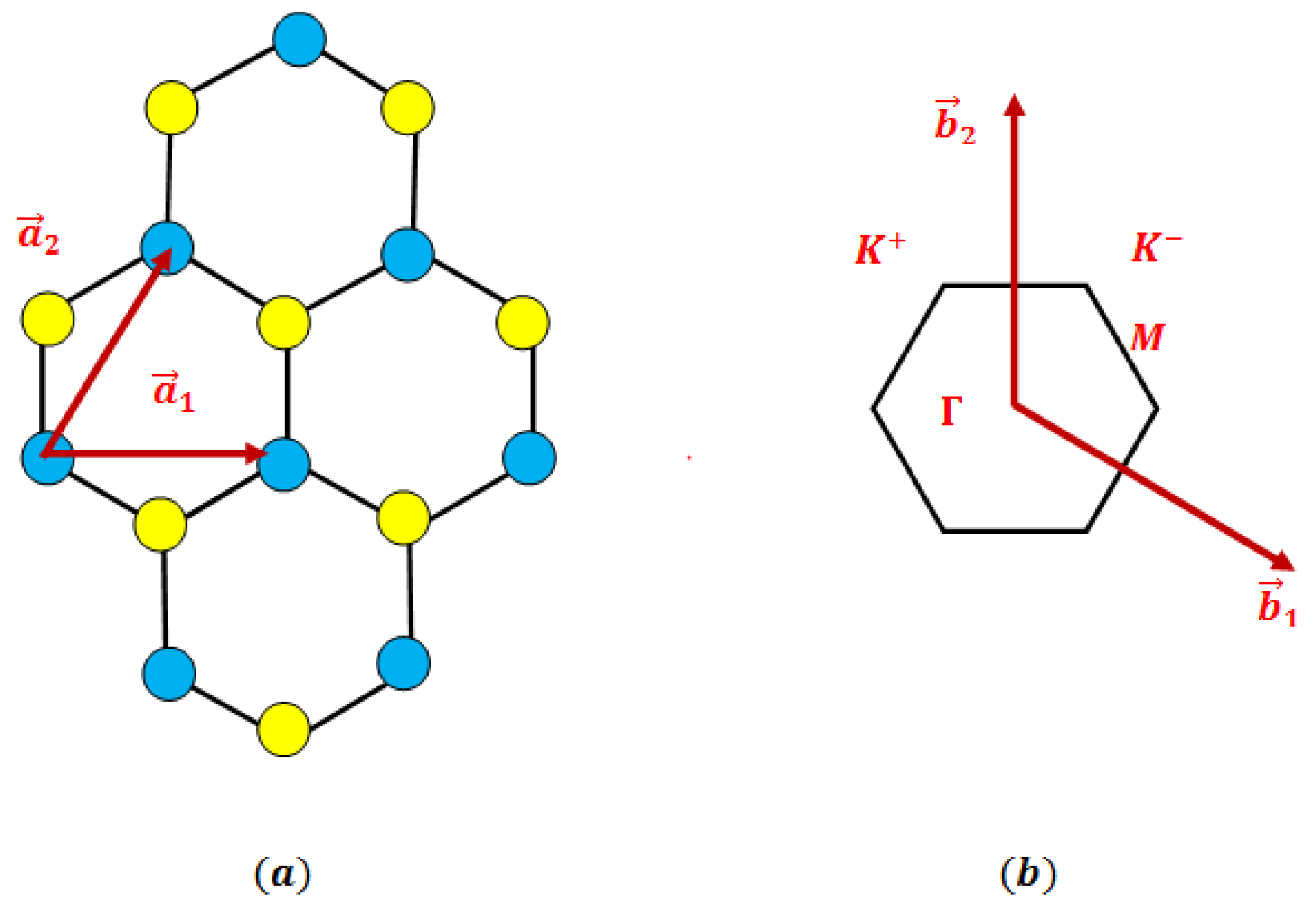
Figure 2.
The strength of the surface optical (SO) coupling between the electronic states ⟩ and as a function of the wave vector in ML PtS2 on SiO2 and hBN polar substrates.
Figure 2.
The strength of the surface optical (SO) coupling between the electronic states ⟩ and as a function of the wave vector in ML PtS2 on SiO2 and hBN polar substrates.
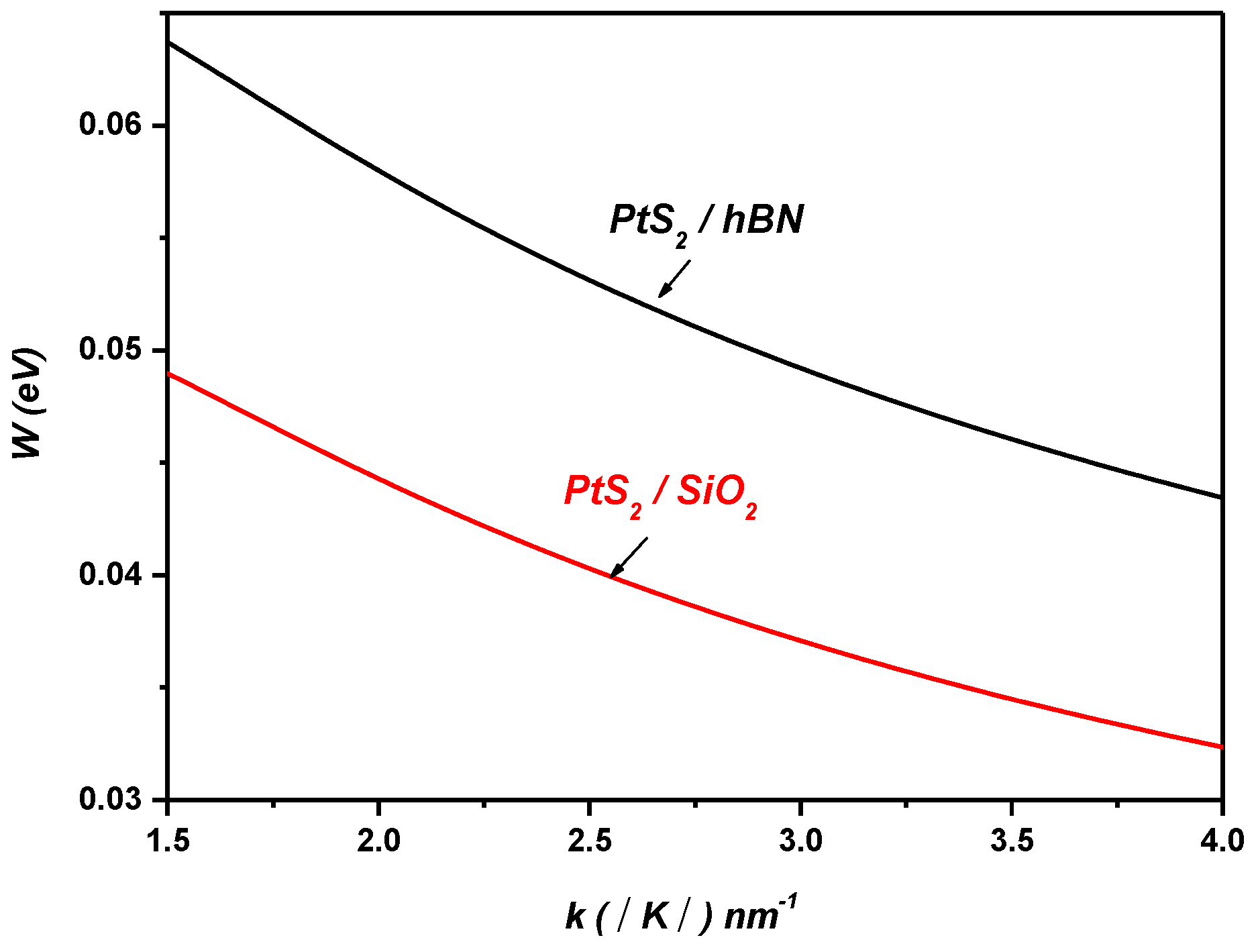
Figure 3.
Polaron electron energies versus the wave vector in the following ML TMDCs on the dielectric polar substrates hBN and SiO2, respectively: (a) and (b) ; (c) and (d) .
Figure 3.
Polaron electron energies versus the wave vector in the following ML TMDCs on the dielectric polar substrates hBN and SiO2, respectively: (a) and (b) ; (c) and (d) .
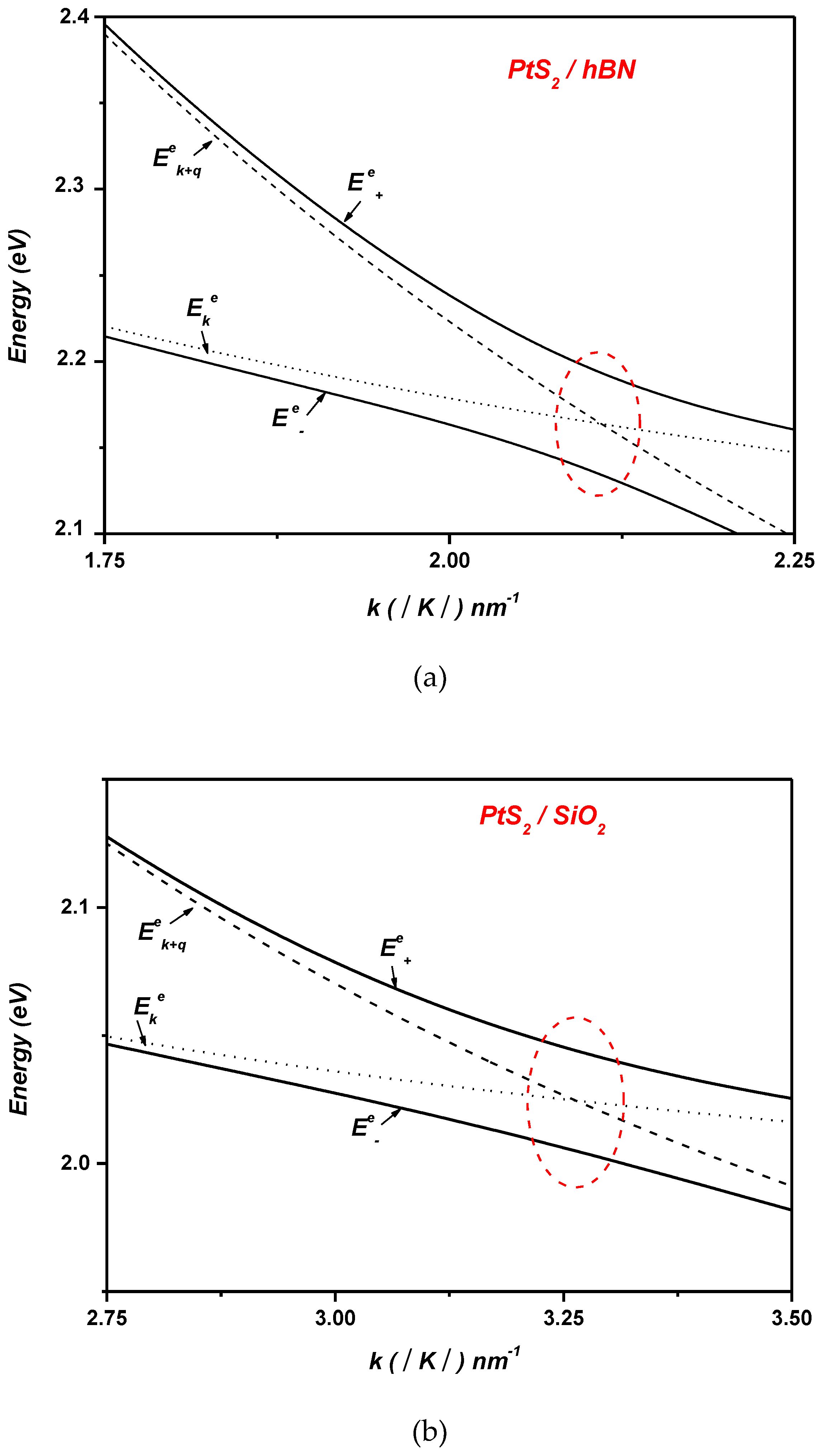
Figure 4.
The weight of the electronic components and the one-phonon components of the lower polaron state in ML and on the and substrates (a) in and (b) in versus the wave vector .
Figure 4.
The weight of the electronic components and the one-phonon components of the lower polaron state in ML and on the and substrates (a) in and (b) in versus the wave vector .
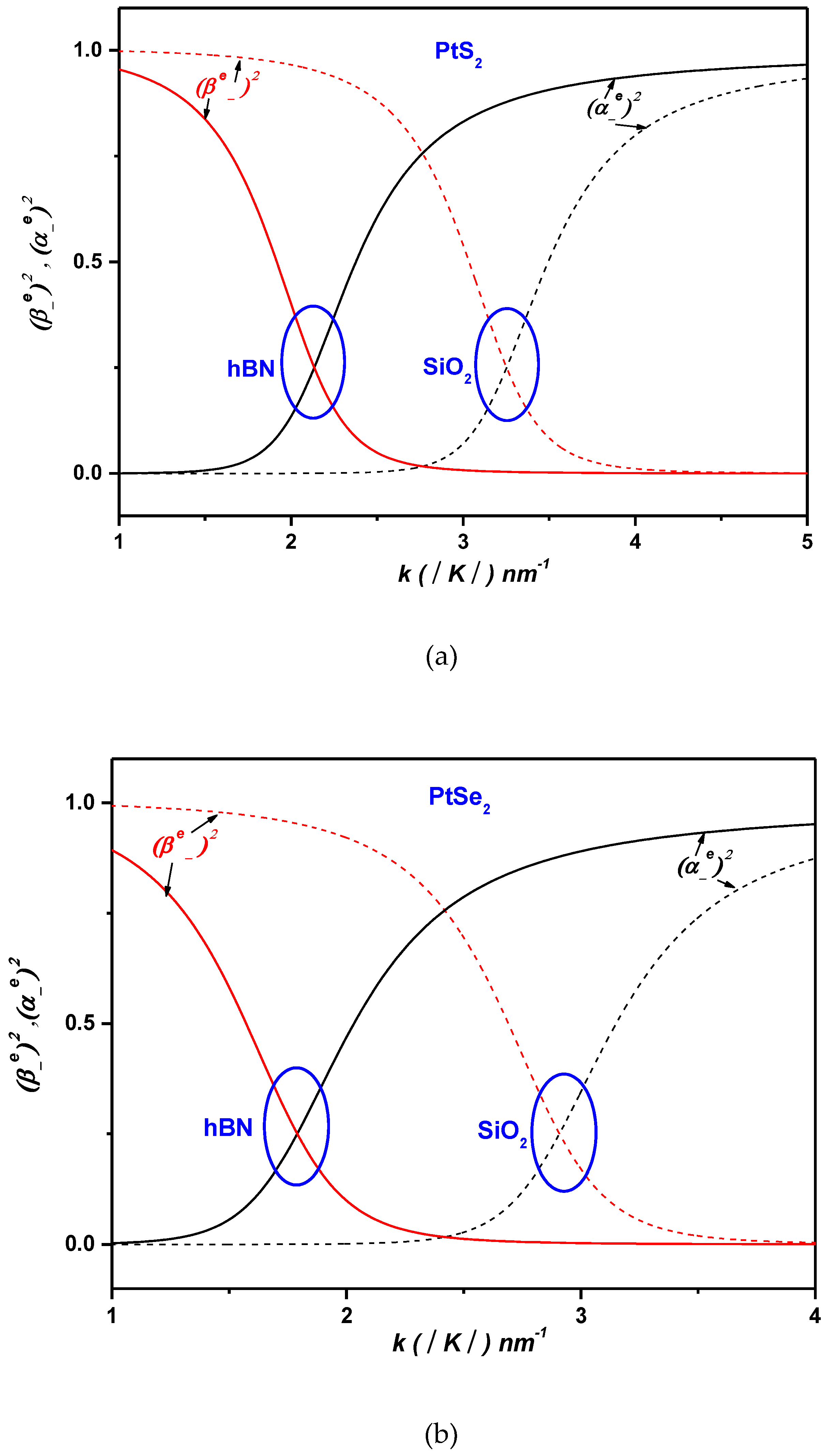
Figure 5.
The polaronic OS of on the and h polar substrates versus the wave vector .
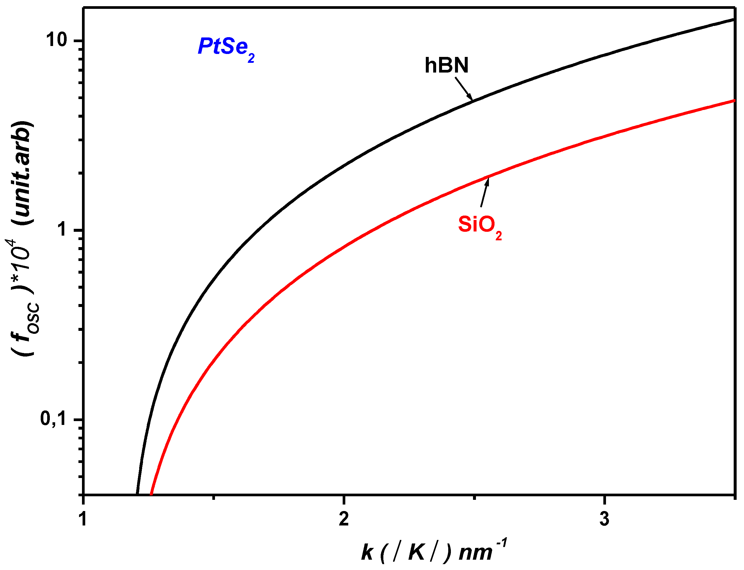
Figure 6.
The polaronic OS in the ML and on polar substrate versus the wave vector .
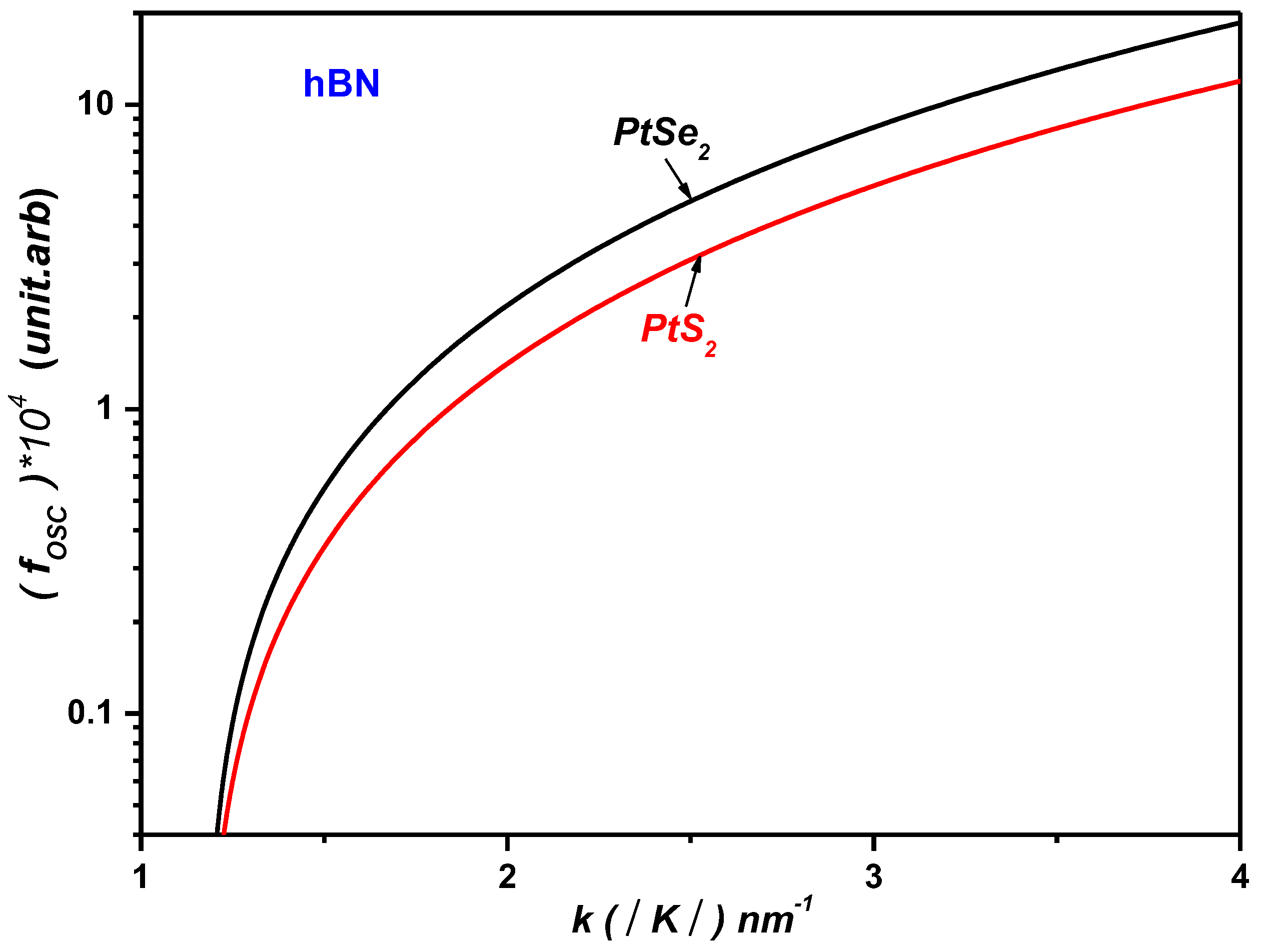
Figure 7.
The temperature dependence of the SO phonon scattering rate in the ML on the and h dielectric polar substrates.
Figure 7.
The temperature dependence of the SO phonon scattering rate in the ML on the and h dielectric polar substrates.
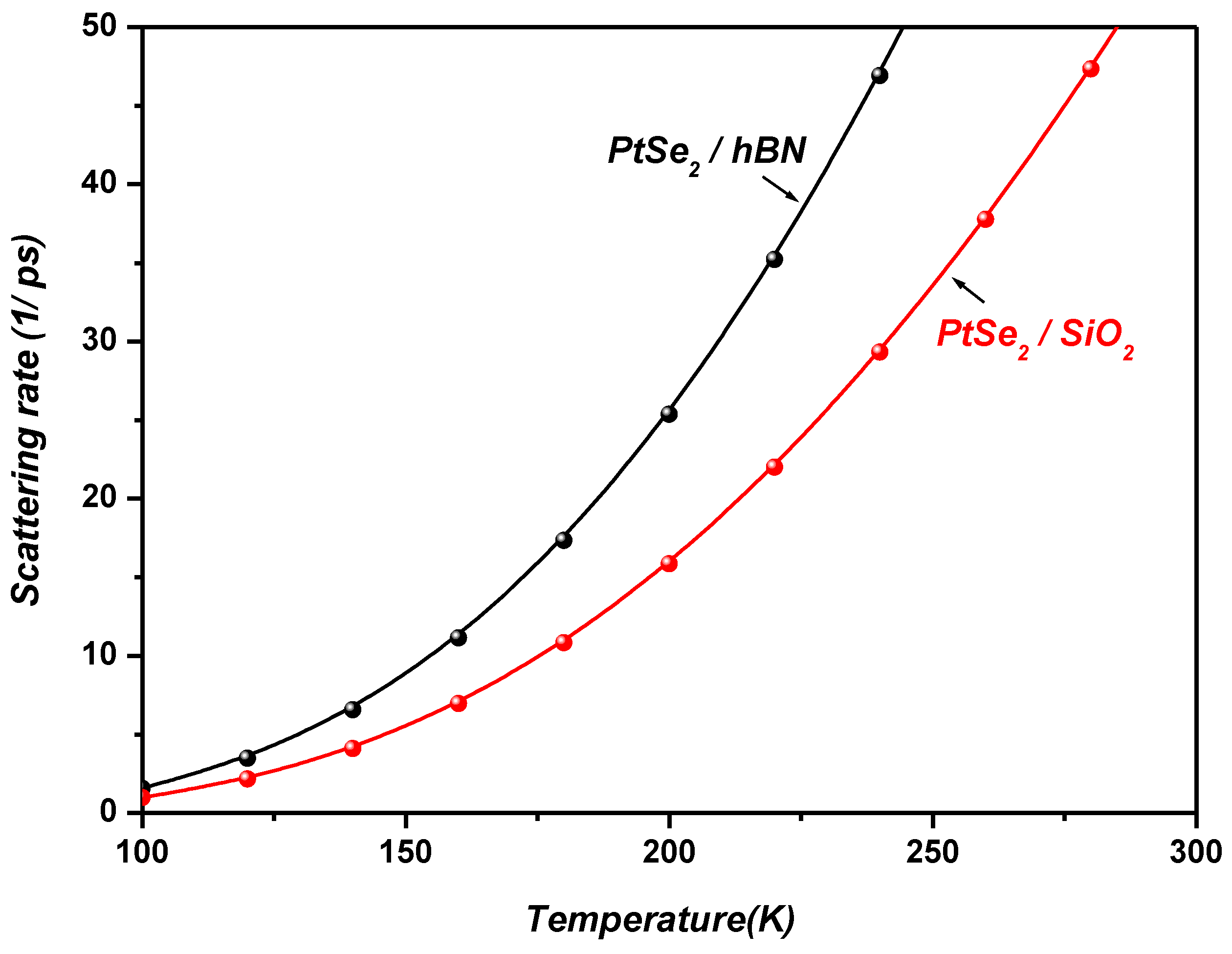
Figure 8.
The SO phonon scattering rate in the ML on the and h dielectric polar substrates as a function of temperature, for various van der Waals (vdW) separation distances.
Figure 8.
The SO phonon scattering rate in the ML on the and h dielectric polar substrates as a function of temperature, for various van der Waals (vdW) separation distances.
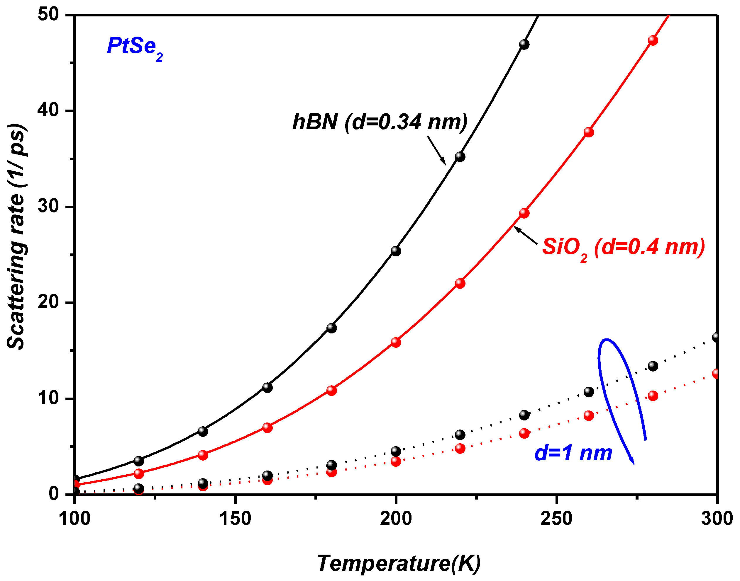

Table 1.
Parameters used for surface polar phonon scattering in monolayer PtSe2 and PtS2 on SiO2 and hBN polar substrates.
Table 1.
Parameters used for surface polar phonon scattering in monolayer PtSe2 and PtS2 on SiO2 and hBN polar substrates.
| 3.9 | 5.09 | |
| 2.4 | 4.1 | |
| 58.9 | 101.7 | |
| 62.5 | 103.7 | |
| 0.237 | 0.258 | |
| 0.4 | 0.34 |
Disclaimer/Publisher’s Note: The statements, opinions and data contained in all publications are solely those of the individual author(s) and contributor(s) and not of MDPI and/or the editor(s). MDPI and/or the editor(s) disclaim responsibility for any injury to people or property resulting from any ideas, methods, instructions or products referred to in the content. |
© 2025 by the authors. Licensee MDPI, Basel, Switzerland. This article is an open access article distributed under the terms and conditions of the Creative Commons Attribution (CC BY) license (http://creativecommons.org/licenses/by/4.0/).
Copyright: This open access article is published under a Creative Commons CC BY 4.0 license, which permit the free download, distribution, and reuse, provided that the author and preprint are cited in any reuse.


