
Submitted:
26 May 2025
Posted:
27 May 2025
You are already at the latest version
Abstract
We present an alternative process for production of binary Nb1−βSnβ superconducting phases using pre- and post-treatment of arc melted Nb+Sn ingots. This process combines sequential sintering, arc melting, and annealing procedures that provide dense, bulk samples of Nb1−βSnβ with varying stoichiometry between 0.18 < β < 0.25 depending on annealing time and temperature. We show, through magnetization measurements of these Nb1−βSnβ bulks, that annealing of arc-melted samples at 900 °C for 3 hours significantly enhances Jc values compared with arc-melted Nb1−βSnβ samples without annealing. Microstructural analyses show that optimum grain size and orientation is achieved by sintering and annealing at lower temperatures (i.e. 720 oC and 900 oC, respectively) with short annealing times (i.e. < 10 hours). Processing at higher temperatures and for longer times enhances grain growth and fewer pinning centres. This process creates effective pinning centres that deliver a Jc = 0.61×10⁵ A/cm2 at 10 K, compared to Jc = 0.34×10⁵ A/cm2 for Nb1−βSnβ subjected to a longer annealing time at a higher temperature and Jc = 775 A/cm2 for an arc melted sample without post-annealing. We suggest that further work addressing post-treatment annealing times between 3 hr < tpost < 60 hr at temperatures between 900 oC and 1000 oC will offer opportunity to control stoichiometric and microstructural imperfections in bulk Nb1−βSnβ materials.
Keywords:
Superconductor
; bulk Nb3Sn
; Arc melting
; Stoichiometry
; Critical current density
; Microstructures
1. Introduction
Nb3Sn was discovered more than half a century ago [1] and continues to hold a crucial role in applications involving high-field magnets. These applications include nuclear magnetic resonance spectroscopy [2], Future Circular Colliders [3], and the International Thermonuclear Experimental Reactor (ITER) [4]. Nb3Sn is an intermetallic compound of niobium and tin with an A15-type structure that enables superconductivity without anisotropy in wire applications [5]. Of the common low-temperature superconducting materials, Nb3Sn has a higher Jc and higher Tc but is very brittle compared with ductile NbTi material [6].
The primary use of Nb3Sn is as superconducting wires for high magnetic field applications [7]. Effective application has built upon fundamental studies [5,8] of the binary Nb–Sn system and recognition that wire manufacture requires utilisation of a ternary system such as Nb–Cu–Sn or Nb–Ti–Sn [5,7,9,10,11]. For example, the bronze route to synthesis using Cu, enables production of Nb1−βSnβ compositions (including Nb3Sn) by moderating the chemical potential of component elements, particularly that of Sn [12]. An excellent summary of reaction behaviours of Nb3Sn in wire processing via the bronze route and by other techniques is provided by Banno [12].
The synthesis of binary Nb3Sn as bulk material is a challenge due to the high diffusivity of Sn and other phases such as NbSn2 with consequent departure from Fick’s law [12]. These challenges led Devantay et al. [8], Goldacker et al. [13] and others to explore novel syntheses to produce homogeneous bulk Nb3Sn. For example, by using levitation melting at high Argon pressure [8] or by utilizing a hot isostatic press (HIP) at 1100 °C [13]. To further minimize inhomogeneity, Zhou et al. [14] also employed a HIP process capable of reaching temperatures up to 2200 °C in combination with ball milling and pre-annealing of starting materials.
Arc melting is an alternative synthesis technique [15] that offers rapid in situ melting to very high temperatures and rapid solidification with minimal element losses. The technique is readily available for laboratory use and is a well-established, scalable industrial process for many alloys and intermetallics [15]. In this work, we evaluate pre-treatment preparation, arc melting of pre-treated samples and annealing times before and after arc melting to explore suitability for effective binary production of bulk Nb3Sn material. To determine stoichiometry of specific phases in these bulk samples, we use high spatial and analytical precision electron microprobe analyses in addition to spatially resolved crystallographic parameters that enable sub-micrometre delineation of microstructure and phase relations.
2. Materials and Methods
A molar ratio of niobium powder (45 μm, 99.8% purity) and tin powder (< 325 mesh size, 99.8% purity) supplied by Sigma-Aldrich are weighed, ground in an agate mortar in an Argon filled glove box, and pressed into a pellet under an applied pressure of 10 Tonne for 2 minutes. Since the difference in melting temperature of Sn and Nb is large, arc melting may cause deviations from intended stoichiometry due to vaporization or loss of Sn. Therefore, pre-annealing is performed on all samples to reduce the potential for Sn evaporation. Two sets of samples are prepared using a mixture of 3:1 stoichiometric Nb+Sn, heat treated at (i) 720 oC for 105 h and (ii) 1000 oC for 60 h under an Ar atmosphere.
These sintered pellets are then melted in an arc furnace on a water-cooled copper hearth under argon. The use of a water-cooled hearth with the arc melting technique helps reduce contamination from the crucible that contains the starting mixture, and allows for easy removal of oxygen from the surrounding gas in the arc furnace. Prior to arc melting experiments, the chamber is vented and filled with argon three times and then filled with argon in order to eliminate oxygen in the chamber. The argon atmosphere was further purified by melting zirconium foam before melting the Nb-Sn pellet. The sample mixture was melted three times to ensure complete mixing. The arc melted samples are then annealed at 900 oC for 3 h and the other samples are annealed at 1000 oC for 60 h. Table 1 lists sample ID and relevant sintering and/or annealing time/temperature of samples.
All samples were subjected to x-ray powder diffraction (XRD) analysis using a Bruker D8 Advance X-ray diffractometer with Co Kα1 radiation in Bragg Brentano geometry. XRD measurements were performed with a step size of 0.02° 2θ and a counting time of 10 s per step. Diffraction patterns were refined and indexed using the software program Topas. Rietveld refinements using Topas determine quantitative estimates of phase abundance in each product. In general, phase abundances determined by this technique are within < 5% relative error.
The microstructures of sintered, arc-melted, and annealed specimens are examined using scanning electron microscopy (SEM) equipped with microanalysis. Microstructural features were examined on polished samples using a field emission JEOL 7001SEM (JEOL Australasia Pty Ltd., French’s Forest, Australia), equipped with a secondary X-ray detector (Oxford Instruments SDD XMax 50 mm2, Abington, UK) and an electron backscatter diffraction (EBSD) pattern analyzer with Channel 5 analysis software and automated feature detection. Finely polished samples mounted in conductive resin are selected for EBSD mapping using an accelerating voltage of 25 kV and a step size of 0.2 µm.
Quantitative elemental analyses are performed using a JEOL JXA 8530F field emission electron probe microanalyzer (FE-EPMA, JEOL, Tokyo, Japan) equipped with five wavelength-dispersive spectrometers (WDS) and using Probe for EPMA software (Eugene, OR, USA). Operating conditions are 10kV accelerating voltage, with a beam current of 40 nA and a fully focused beam. Wavelength dispersive analysing crystals are PETL for Nb La, and PETH for Sn La, and calibration standards include pure Nb and Sn metals. On- and off-peak counting times are 30 s, and a linear off-peak correction method is employed for background positions selected on either side of the analytical peaks. Average detection limits (single spot, 3-sigma) are 360 ppm for Nb and 390 ppm for Sn, with analytical sensitivity (at the 99% confidence interval) of 0.3 % relative. Estimated spatial precision for each analysis based on earlier Monte Carlo simulations of secondary X-ray trajectories [16] is < 1.5 μm. For these analyses, the samples are combined with conductive resin and positioned in a 30 mm diameter mould within a hot mounting press. The mounted samples are then polished using a sequence of diamond pads and cloths to achieve a mirror-like finish, which is ideal for electron microprobe analysis.
Zero field cooled (ZFC) and field cooled (FC) magnetization (M) curves are recorded as a function of temperature at 10 Oe using a Cryogenic Ltd. Mini Cryogen-free System (Cryogenic Ltd., London, UK) with a 5 Tesla magnet. Tc was determined by finding the intersection of the linearly extrapolated M(T) with constant M line. Magnetic hysteresis loops were measured at several temperatures below Tc for all samples. A magnetic Jc was calculated for samples using the Bean model: Jc = 20 ΔM/ [V.a(1- a/3b)] (a < b), where a and b are the width and length of the sample perpendicular to the applied field, respectively. V is the sample volume and ΔM is the amplitude of the magnetic hysteresis loop.
3. Results
Table 1 summarizes information regarding selected sample IDs, synthesis techniques and heat treatment conditions for Nb3Sn bulks reported in this study. For instance, the sample ID “NS-1000/60” represents a Nb+Sn mixture sintered at 1000 °C for 60 hours with no arc melting process, while the ID “NS-1000/60/arc” represents a sample that has been subject to arc melting after a sintering process at 1000 oC for 60 hours.
Two sintering temperatures, at 720 oC and 1000 oC, have been evaluated for this work to explore both lower and higher sintering temperature effects. Preliminary evaluation showed that a Nb–Sn phase did not form with sintering at 720 oC. Nevertheless, NS-720/105/arc/ann/900/3 is prepared from an arc-melted sample where Nb+Sn mixtures are sintered at 720 °C for 105 hours before arc melting, followed by annealing at 900 oC for 3 hours. The sample ID NS-1000/60/arc/ann/1000/60 represents a sintered sample at 1000 °C for 60 hours with arc melting and an annealing treatment at 1000 °C for 60 hours.
3.1. Crystallography and Phase Relations
Results from a Rietveld refinement to quantitatively determine phase abundances is shown in Figure 1 for the XRD pattern from NS-1000/60/arc/ann/1000/60 (Run 3). The blue, red and grey colours represent experimental, refined, and difference in models, respectively. As shown in Figure 1, Nb3Sn is the predominant phase (94.88%) with denoted indexed reflections while a minor proportion of secondary phase such as niobium oxide is also observed (green symbols). Similar refinements were performed for all other samples including those with a high proportion of Nb3Sn phase.
Table 2 shows the relative proportions of Nb3Sn and other products obtained from selected syntheses with a high proportion of Nb3Sn phase based on indexed XRD patterns. Refined XRD data including change in lattice parameters, weighted R factor (Rwp) and goodness of fit (gof) for each refinement are also shown in Table 2. Run 4 is not included in Table 2 because diffraction from a Nb3Sn phase was not observed. The sample from Run 5 was damaged during sample preparation for characterisation and is also not included in Table 2.
In all cases, Nb3Sn is the major phase (in proportions above 85%) with minor amounts of other compounds including Nb and NbO. An increase in reaction time for NS-1000/60/arc/ann/1000/60 (Run 3) improves the yield of Nb3Sn due to complete conversion of excess Nb. The lattice parameter a decreases for arc melted and annealed samples compared with a sample sintered at 1000 oC for 60 h (NS-1000/60; Run 1). Note the relatively high proportions of unreacted Nb for samples NS-1000/60/arc (Run 2) and NS-720/105/arc/ann/900/3 (Run 6).
3.2. Microstructures and Grain Compositions
EBSD phase maps of Nb3Sn bulks for sintered, arc melted and annealed samples are shown in Figure 2. For all samples, Nb3Sn is the major phase and confirms XRD Rietveld analyses that >85% of all samples are Nb3Sn. According to EBSD analysis, minor phases Nb, Sn and NbO are present in all samples. Diffraction peaks for Sn have not been detected in XRD patterns. The discrepancy in detecting Sn by diffraction methods may be due to a localized presence on the surface of samples, low concentration or an amorphous structure. In the latter case, Sn is detectable via EBSD but not by using XRD.
Irregular Nb3Sn crystals of < 10 μm dimension are formed together with Nb and NbO in samples from NS-1000/60 (Figure 2a; Run 1). The presence of large Nb grains (> 30 μm) indicates that an extended sintering process did not eliminate minor phases such as Nb or NbO. In Figure 2a, black areas (indicated by white arrows) indicate the presence of pores in these sintered samples. The microstructure of the NS-1000/60/arc (Figure 2b; Run 2) shows the formation of Nb and Sn phases along with Nb3Sn phase as well as a more consolidated microstructure with fewer pores than in Figure 2a. Most solidification morphologies due to arc melting conditions possess an approximate hemispherical shape.
Figure 2 indicates that arc melting provides higher-density products. Figure 2c, clearly indicates that Nb3Sn grains produced after annealing of the arc melted sample at 900 oC for 3 h (NS-720/105/arc/ann/900/3; Run 6), are significantly smaller (i.e., sub-micrometre to micrometre size) than those (i.e., > 10 μm) produced at a higher temperature (1000 oC) and annealed for a longer time (60 h) as shown for NS-1000/60/arc/ann/1000/60 (Run 3). Extended annealing of the sample at higher temperature of 1000°C for 60 h results in dense packed and large grains (> 50 μm) of Nb3Sn. This morphology is due to significant grain growth, driven by increased atom mobility at the higher annealing temperature over time.
Figure 3 shows Euler maps (determined by the EBSD technique) of Nb3Sn samples listed in Table 2. Euler maps, which represent the crystallographic orientation of individual grains, reveal significant variations among the Nb₃Sn bulk samples subjected to different heat treatments. For the sintered sample NS-1000/60 (Figure 3a), the map shows a wide range of orientations, indicating a lack of common crystallographic orientation among the grains. This Euler map suggests that the sintering process at 1000 °C for 60 h did not result in a uniform texture for all grains, including Nb₃Sn.
The sample NS-720/105/arc/ann/900/3 (Run 6) displays a more uniform crystallographic orientation with three predominant orientations observed for all grains in the field of view (Figure 3c). This texture indicates a more consistent grain orientation resulting from the annealing process. In contrast, the sample with extended annealing at 1000 °C for 60 h after arc-melting (NS-1000/60/arc/ann/1000/60) shows the presence of large Nb₃Sn grains, each exhibiting distinct crystallographic orientations. This grain morphology confirms that prolonged annealing at high temperatures promotes grain growth, resulting in larger grains with diverse orientations. These observations highlight the significant impact of heat treatment protocols on the crystallographic orientation and grain structure of Nb₃Sn samples.
Figure 4 shows backscattered images of four samples listed in Table 1. The backscattered electron (BSE) image displays a broad range of image contrast typically attributed to fluctuations in the relative mean atomic number. Generally, regions appearing lighter in a BSE image have a higher atomic number compared to darker regions. This image contrast also highlights microstructural changes in the Nb3Sn samples due to different processing and annealing conditions. For instance, black colour delineates pores in the sample (Figure 4a), while the dark grey and brighter grey colour denotes the Nb-rich and Sn-rich phases, respectively. In Figure 4a, the BSE image of NS-1000/60 (Run 2) reveals Nb3Sn aggregates surrounded by pores. These aggregates exhibit a distinctive pattern with a dark core and a lighter outer margin, corresponding to Nb-rich and Sn-rich phases, respectively.
A BSE image of the arc melted sample (NS-1000/60/arc; Figure 4b) shows a darker Nb-rich area surrounded by lighter Sn-rich areas (arrowed). Figure 4c shows a BSE image of NS-720/105/arc/ann/900/3 (Run 6) with uniform structure and substantially smaller grain sizes compared to NS-1000/60 (Run 1) and NS-1000/60/arc (Run 2). The BSE image in Figure 4d shows that extended annealing of the arc melted sample at 1000 °C for 60 h (NS-1000/60/arc/ann/1000/60; Run3) resulted in larger grains (i.e., > 20 μm) compared to NS-720/105/arc/ann/900/3 (Figure 4c; Run 6). Note the use of different scale bars in Figure 4.
BSE images in Figure 4 are used to guide locations for EPMA analyses; the locations for which are annotated by a small red dot. Table 3 provides average compositions from selected spot analyses for syntheses identified in Table 1. For each sample, the number of point analyses (n) used to obtain average compositions based on similar BSE image contrast is also listed in Table 3, along with corresponding average analytical totals that range from 98.7 to 99.8 (wt%) for the Nb–Sn phases. A majority of individual point analyses are Nb1−βSnβ phases albeit other analyses are consistent with the presence of Nb and NbO in these samples.
3.3. Electrical and Magnetic Properties
Figure 5a shows the zero-field cooled and field cooled measurements for Nb3Sn bulks under an applied magnetic field of 10 Oe. All samples show a clear superconducting transition similar to that obtained previously [14]. NS-1000/60 (Run 1) and NS-720/105/arc/ann/900/3 (Run 6) demonstrate very sharp superconducting transitions at 16.45 K and 16.58 K, respectively. NS-1000/60/arc/ann/1000/60 (Run 3) shows a slightly lower transition temperature at 16.26 K. The arc melted sample without further annealing (NS-1000/60/arc), shows a broad transition at 16.21 K followed by other transitions at 15.42 K and 6.78 K.
Figure 5b shows the field dependence of Jc for samples arc melted (NS-1000/60/arc; Run 2), annealed at 900 oC for 3 h (NS-720/105/arc/ann/900/3; Run 6) and annealed at 1000 oC for 60 h (NS-1000/60/arc/ann/1000/60; Run 3). As shown in Figure 5b, the Jc of arc melted Nb3Sn is much lower than the Jc of post-annealed Nb3Sn bulks. Both Nb3Sn bulk samples annealed at 900 oC and 1000 oC (NS-720/105/arc/ann/900/3 and NS-1000/60/arc/ann/1000/60) demonstrate enhanced Jc performance compared to only arc melted Nb3Sn (NS-1000/60/arc).
Both annealed samples, NS-720/105/arc/ann/900/3 and NS-1000/60/arc/ann/1000/60, exhibited significantly enhanced critical current density (Jc)—about 1.5 orders of magnitude greater—compared to the arc-melted sample (NS-1000/60/arc; Run 2). NS-720/105/arc/ann/900/3 demonstrated the highest Jc across the entire field range up to 5 T. Specifically, at 10 K, the low-field and high-field Jc values for NS-720/105/arc/ann/900/3 (Run 6) were 1.8 times and 5.8 times higher, respectively, than comparable values for NS-1000/60/arc/ann/1000/60 (Run 3).
Electrical resistance, R, versus temperature, T, curves for samples from NS-720/105/arc/ann/900/3 (Run 6) and NS-1000/60/arc/ann/1000/60 (Run 3) in the presence of magnetic fields up to 5 T are shown in Figure 6a and 6b. Electrical resistance starts to drop toward zero at Tc= 18.0 K in zero magnetic field for both samples. This value aligns well with reports for the onset of superconductivity at 18.05 K ± 0.1 reported by Matthias et al. [1]. The onset of Tc decreases with increasing magnetic field, while the transition width, ΔTc, increases from 0.1 K to 0.4 K for both samples as shown in Figure 6a and 6b.
Figure 6c shows estimates for the upper critical field, Hc2, defined by R(T, Hc2) = 0.9Rn, represents the normal state resistance measured just above the onset of the critical temperature. Similarly, the irreversibility field, Hirr, is defined by R(T,Hirr) = 0.1Rn and is also shown in Figure 6c. From Figure 6c, we calculated slopes of 2.09 and 1.89 for dHc2/dT and dHirr/dT, respectively, for NS-720/105/arc/ann/900/3 (Run 6). Similarly, NS-1000/60/arc/ann/1000/60 yielded values of 2.05 and 1.85 T/K for dHc2/dT and dHirr/dT.
The Hc2 (0) is estimated using the Werthamer-Helfand-Hohenberg formula, Hc2 = -0.69Tc(dHc2/dT), with dHc2/dT at T = Tc. Using this formula, values for Hc2(0) = 26.1 and 25.6 T are obtained for the sample from NS-720/105/arc/ann/900/3 (Run 6) and NS-1000/60/arc/ann/1000/60 (Run3), respectively. These values are lower than the reported value of 28.7 T for 23.6 ± 0.7 at.% Sn composition variation, noting that bulk samples in the study by Jewell et al. [17] were obtained using HIP techniques at 1020 oC on powder-in-tube samples followed by post-HIP heat treatment at 1800 oC for 24 hours.
4. Discussion
In this work, we show combinations of sintering, arc-melting and annealing procedures that affect the morphology, stoichiometry and superconducting properties of bulk Nb3Sn samples. Sintering of Sn and Nb is undertaken prior to arc melting in order to mitigate Sn evaporation at higher temperatures. The Nb–Sn phase diagram indicates that the superconducting Nb1−βSnβ phase occurs within the range for 0.18 < β < 0.25 for which 6 K < Tc < 18 K [5]. This phase can be synthesized either above 930 °C in the presence of a Sn–Nb melt or below this temperature through solid-state reactions involving Nb and Nb6Sn5 or NbSn2 [12].
4.1. Structure and Composition
The formation of Nb3Sn is not favourable for the sample sintered at 720 °C for 105 h (data not shown) because the diffusion of Nb and Sn is relatively slow. However, Nb3Sn is a primary phase of the sample sintered at 1000 oC (NS-1000/60) prior to arc melting according to XRD and EBSD phase analysis. A higher sintering temperature of 1000 °C prior to arc melting promotes faster diffusion and effective transformation of the starting mixture. After arc melting, the sample shows a high proportion of Nb3Sn phase and the presence of residual Nb and Sn (as shown in Figures 2b, 3b and 4b) albeit with a lower proportion of Nb3Sn compared to Run 1 or Run 3. In addition, EPMA analyses (Table 3) show that individual grains are marginally within the superconducting range for Nb1−βSnβ phases (i.e., β =18.6(1)).
Post-annealing serves as an important step to stabilize metastable phases that form during quenching and facilitates the formation of the target composition. In both cases, for Run 3 and Run 6, annealing after arc melting results in compositions for Nb1−βSnβ phases within the superconducting range [5]. However, a substantial difference in grain size is observed between both samples. Annealing of NS-720/105/arc/ann/900/3 (Run 6) at 900 °C yields a uniform microstructure with smaller (< 5 μm) grain sizes.
Goedeke [5] provided a comprehensive and informative review of early experiments on production of homogenous Nb3Sn, noting that the general variation of superconducting properties for A15 compounds consistently depends on cell dimension, atomic content (for Nb1-βSnβ, the value of β), normal state resistivity and long range order. Figure 7 is an adaptation of Figure 3 in [5] showing the variation of lattice parameter, a, with atomic content of Sn in Nb1−βSnβ. Figure 7 includes average data for individual grains within the four samples that show compositions within the range 0.18 < β < 0.25 (Table 3).
Interpretation of Figure 7 suggests that pre-treatment of Nb–Sn ingots before arc melting combined with post-treatment annealing may enable production of bulk Nb1−βSnβ with a targeted stoichiometry. For example, Rietveld (Table 2) and EPMA compositional (Table 3) analyses show that Run 1 produces a predominantly β = 0.25 compound with pre-treatment. Arc melting of this sample produces a mixture with lower proportions of Nb1−βSnβ with β = 0.186 and substantial Nb. Annealing after arc melting results in a sample with high proportions of two Nb1−βSnβ compounds (Table 3) with β = 0.226 and β = 0.203. These trends are shown in Figure 7 by the broad dotted red arrows and suggests that further attention to annealing times post-arc melting could result in a bulk single phase Nb1−βSnβ compound.
The optimum annealing times and appropriate temperatures to maximise single phase Nb3Sn remains uncertain based on data obtained to date. Nevertheless, the example of Run 6 from which predominantly Nb1−βSnβ forms with β = 0.231 after a lower temperature pre-treatment and a lower temperature and very short annealing time implies that within the extremes of processing represented by Run 3 and Run 6, evaluation of these parameters is prospective for scalable production of bulk Nb3Sn. In the latter case, smaller micrometre-scale grain size and enhanced Jc compared to other samples of this study suggest that annealing times, tpost, 3 hr < tpost < 60 hr at temperatures between 900 oC and 1000 oC are viable targets for future experiments.
4.2. Superconductivity
The arc melted sample for NS-1000/60/arc (Run 2) exhibits a wide superconducting transition at 16.21 K, accompanied by additional transitions at 15.42 K and 6.78 K. The low Tc = 6.78 K could be due to formation of a solid solution with lower Tc associated with lower Sn content (β = 0.104) as indicated by EPMA data (see Table 3). It is reported that at low concentrations (β < 0.05 for Nb1-βSnβ), the incorporation of Sn into Nb forms a solid solution that lowers the Tc of Nb from 9.2 K to approximately 4 K for β= 0.05 [5,12,18].
In the A15 Nb3Sn structure, which has a lattice parameter of about 0.529 nm for the stoichiometric composition [8], the separation between Nb atoms is roughly 0.265 nm. This reduced distance between Nb atoms in the chains is believed to create a confined peak in the d-band density of states (DOS), resulting in a notably increased DOS near the Fermi level. This enhancement is thought to play a role in the higher critical temperature (Tc) of Nb3Sn compared to other Nb-based superconductors. Additionally, it has been observed that excess Nb atoms can occupy Sn sites, leading to anti-site disorder [19].
Ab initio density functional theory (DFT) calculations by Besson et al. [22] reveal that Nb3Sn essentially appears as an anti-site compound, with the density of vacancies, particularly Sn vacancies, remaining negligible below the melting temperature [20]. Additionally, an EXAFS study examining the occupancy of Ta/Ti sites in Nb3Sn wires reveals that the top-performing Ti-doped strand is considerably sub-stoichiometric in Sn [21]. This anti-site disorder is likely responsible for the high average behaviour of the upper critical field (Hc2). EPMA analyses (Table 3) show non-stoichiometric compositions in samples from Runs 2, 3 and 6; implicit confirmation that the density of vacancies and/or anti-site disorder influence electronic properties of Nb1−βSnβ compounds. These findings suggest that dopants and anti-site disorder play a crucial role in minimizing the variability of superconducting properties and maximizing high-field Jc properties.
Table 4 shows a comparison between experimental data and calculated Tc using DFT from the work of Carlson et al. [22] and Tc values obtained for samples in this work. The Sn concentration according to EPMA results (Table 3) can be correlated with the experimental determination of Tc [20]. For both DFT calculations and experimental results in our work, Tc values increase with increasing Sn concentration. The calculated Tc and the Fermi level DOS show strong agreement across all Sn concentrations [22]. The presence of Sn anti-site defects is believed to significantly broaden a reduction in the density of states (DOS) at the Fermi level near grain boundaries [22]. This presence of anti-site defects may explain the reduction in Tc from 16.58 K for Nb3.00Sn (NS-1000/60; Run 1) to 16.25 K for Nb3Sn0.88 + Nb3Sn0.77 (NS-1000/60/arc/ann/1000/60; Run 3).
The Jc of a bulk superconductor in a magnetic field is governed by the pinning force (Fp) generated by appropriately sized crystal defects, which hinder the movement of magnetic vortices. The efficiency of pinning is highest when defects approach the coherence length of a superconductor, typically 2–4 nm for Nb3Sn [23]. Defects smaller or larger than this size result in reduced pinning efficiency. Grain boundaries, which are the regions where different crystal grains meet, can also act as pinning centres for magnetic flux lines. The significant impact of grain boundaries on the superconducting properties of Nb3Sn is widely recognized [24]. These boundaries play a crucial role in pinning vortices and determining critical currents in Nb3Sn wires, as documented in previous studies [5,25,26] and experimentally demonstrated using atom probe tomography combined with Jc measurements on Nb3Sn wires synthesised by the internal tin process [24].
The enhanced Jc of the bulk sample from NS-720/105/arc/ann/900/3 (Run 6) is related to the formation of smaller grains (i.e., < 5 μm) and a higher density of grain boundaries compared with the arc melted and post-annealed Nb1−βSnβ sample synthesised at higher temperature. The NS-1000/60 (Run 1) and NS-1000/60/arc (Run 2) with large grains show a lower Jc compared with NS-720/105/arc/ann/900/3 (Run 6), especially at higher magnetic fields.
Simulation by Carlson et al. [22] demonstrates that grain boundaries serve a dual role: they act as nucleation points for vortex entry and as pinning sites once vortices have formed. The behaviour of the vortices depends on the strength of the applied field—vortices can either stay pinned at the grain boundaries or pass into the grains. This interpretation is consistent with higher supercurrent loss for NS-1000/60/arc/ann/1000/60 (Run 3) compared with NS-720/105/arc/ann/900/3 (Run 6) for H > 2 T. Additionally, observations have revealed compositional variations within Nb3Sn grain boundaries at a nanometer scale [27,28] that affect the supercurrent performance of Nb3Sn superconducting wires. Among the samples studied, NS-720/105/arc/ann/900/3 (Run 6) with an average Nb3Sn0.9 composition shows the highest supercurrent performance which could be due to the presence of anti-site defects.
5. Conclusions
This investigation explored the impact of synthesis procedures using pre-treatment, arc melting and post-arc melt annealing on the morphology, grain boundary formation and stoichiometry of binary Nb1−βSnβ bulk superconductors. An arc-melted sample annealed at 900 °C for 3 hours (β = 0.231) results in enhancement of Tc and Jc compared to other samples in this work. This enhancement is attributed to recrystallization of smaller grains and formation of effective pinning centres such as a higher proportion of grain boundaries and anti-site defects. However, annealing at 1000 °C for 60 hours after arc melting reduced Jc. A decrease in Tc from 16.58 K for Nb3.00Sn in a sintered binary sample to 16.25 K for an arc melted and annealed sample is attributed to production of two Nb1−βSnβ compounds (β = 0.226 and β = 0.203) of large grain size (> 50 μm) and no Nb. These two alternate synthesis procedures—involving pre-treatment sintering, followed by arc melting and subsequent annealing at high temperature (> 900 oC) for different times—suggests that further exploration of sintering and annealing conditions offers potential for scalable production of bulk Nb1−βSnβ compounds of predictable stoichiometry.
Author Contributions
MS: conceptualisation, formal analysis, methodology, investigation, supervision, funding acquisition, writing—original, review and editing; HEC: EPMA methodology and analysis, investigation, validation and visualization; ADM: methodology, investigation, resources, validation; JA: investigation, formal analysis, review and editing; IDRM: conceptualisation, formal analysis, funding acquisition, validation, visualization, writing—review and editing.All authors have read and agreed to the published version of the manuscript.
Funding
This research was partially funded by an Advance Queensland Research Fellowship from the Queensland Government to MS and from the Australian Government agency ARENA as part of Contract No. 2018/RND012. The views expressed herein are not necessarily the views of the Australian Government, and the Australian Government does not accept responsibility for any information or advice contained herein.
Data Availability Statement
The data supporting the conclusions of this study are presented within the article. Comprehensive EPMA results can be provided upon request.
Acknowledgments
The authors are grateful to the Central Analytical Research Facility at Queensland University of Technology for access to characterization facilities. During the preparation of this manuscript and study, the author(s) did not use any artificial intelligence tools. The authors have reviewed and edited the output and take full responsibility for the content of this publication.
Conflicts of Interest
The authors declare no conflicts of interest. The funders of this study had no role in the design of the study; in the collection, analyses, or interpretation of data; in the writing of the manuscript; or in the decision to publish the results.
References
- Matthias, B.T., Geballe, T.H., et al., Superconductivity of Nb3Sn, Physical Review 1954 95 6 1435-1435.
- Miyazaki, T., Matsukura, N., et al., Development of Bronze-Processed Nb3Sn Superconductors for 1GHz NMR Magnets, in: Balachandran, U.B., et al. (Eds.), Advances in Cryogenic Engineering Materials, Springer US, Boston, MA, 1998, pp. 935-941.
- Tommasini, D. , Nb3Sn Accelerator Dipole Magnet Needs for a Future Circular Collider, in: Schoerling, D., Zlobin, A.V. (Eds.), Nb3Sn Accelerator Magnets: Designs, Technologies and Performance, Springer International Publishing, Cham, 2019, pp. 427-439.
- Mitchell, N.; Breschi, M.; Tronza, V. The use of Nb3Sn in fusion: lessons learned from the ITER production including options for management of performance degradation. Supercond. Sci. Technol. 2020, 33, 054007. [Google Scholar] [CrossRef]
- Godeke, A. , A review of the properties of Nb3Sn and their variation with A15 composition, morphology and strain state, Superconductor Science and Technology 2006 19 8 R68-R80.
- Sun, W.; Cheng, J.; Chen, S. Preparation and Superconducting Properties of Nb3Sn by Mechanical Alloying. J. Low Temp. Phys. 2021, 205, 100–111. [Google Scholar] [CrossRef]
- Flükiger, R.; Uglietti, D.; Senatore, C.; Buta, F. Microstructure, composition and critical current density of superconducting Nb3Sn wires. Cryogenics 2008, 48, 293–307. [Google Scholar] [CrossRef]
- Devantay, H.; Jorda, J.L.; Decroux, M.; Muller, J.; Flükiger, R. The physical and structural properties of superconducting A15-type Nb-Sn alloys. J. Mater. Sci. 1981, 16, 2145–2153. [Google Scholar] [CrossRef]
- Flukiger, R.; Schauer, W.; Specking, W.; Schmidt, B.; Springer, E. Low temperature phase transformation in Nb3Sn multifilamentary wires and the strain dependence of their critical current density. IEEE Trans. Magn. 1981, 17, 2285–2288. [Google Scholar] [CrossRef]
- Cheng, J.; Wang, Q.; Wang, H.; Dai, Y. Microstructure evolution of Nb3Sn superconductors during diffusion treatment by bronze route. Rare Met. 2012, 31, 446–450. [Google Scholar] [CrossRef]
- Wu, B.; Guo, Q.; Wang, C.; Chen, J.; Li, Z.; Shi, Y.; Liu, X.; Feng, Y.; Yan, G.; Li, J.; et al. Investigation on the Recrystallization and Nb3Sn Microstructure of Nb Alloys With Large Deformation During Heat Treatment. IEEE Trans. Appl. Supercond. 2024, 34, 1–4. [Google Scholar] [CrossRef]
- Banno, N. Low-temperature superconductors: Nb3Sn, Nb3Al, and NbTi. Superconductivity 2023, 6. [Google Scholar] [CrossRef]
- Goldacker, W.; Ahrens, R.; Nindel, M.; Obst, B.; Meingast, C. HIP synthesized Nb/sub 3/Sn bulk materials with extraordinary homogeneity. IEEE Trans. Appl. Supercond. 1993, 3, 1322–1325. [Google Scholar] [CrossRef]
- Zhou, J.; Jo, Y.; Sung, Z.H.; Zhou, H.; Lee, P.J.; Larbalestier, D.C. Evidence that the upper critical field of Nb3Sn is independent of whether it is cubic or tetragonal. Appl. Phys. Lett. 2011, 99, 122507. [Google Scholar] [CrossRef]
- Jain, D. , Sudarsan, V., et al., Synthesis of Metallic Materials by Arc Melting Technique, in: Tyagi, A.K., Ningthoujam, R.S. (Eds.), Handbook on Synthesis Strategies for Advanced Materials : Volume-I: Techniques and Fundamentals, Springer Singapore, Singapore, 2021, pp. 197-213.
- Shahbazi, M.; Cathey, H.E.; Mackinnon, I.D.R. Synthesis of Magnesium Nickel Boride Aggregates via Borohydride Autogenous Pressure. Materials 2018, 11, 480. [Google Scholar] [CrossRef] [PubMed]
- Jewell, M.C. , Godeke, A., et al., The upper critical field of stoichiometric and off-stoichiometric bulk, binary Nb3Sn, Joint Cryogenic Engineering Conference/International Cryogenic Materials Conference (CEC-ICMC) Anchorage, AK, 2003, pp. 474-481.
- Foner, S. , Schwartz, B., Superconductor Materials Science: Metallurgy, Fabrication, and Applications, Springer New York, NY1981.
- Welch, D.O. , Dienes, G.J., et al., Defects and diffusion mechanisms in Nb3Sn, Journal of Physics and Chemistry of Solids 1984 45 11 1225-1242.
- Besson, R. , Guyot, S., et al., Atomic-scale study of diffusion in A15 Nb3Sn, Physical Review B 2007 75 5 054105.
- Heald, S.M.; Tarantini, C.; Lee, P.J.; Brown, M.D.; Sung, Z.; Ghosh, A.K.; Larbalestier, D.C. Evidence from EXAFS for Different Ta/Ti Site Occupancy in High Critical Current Density Nb3Sn Superconductor Wires. Sci. Rep. 2018, 8, 1–9. [Google Scholar] [CrossRef]
- Carlson, J. , Pack, A., et al., Analysis of magnetic vortex dissipation in Sn-segregated boundaries in Nb3Sn superconducting RF cavities, Physical Review B 2021 103 2 024516.
- Xu, X.; Peng, X.; Rochester, J.; Lee, J.-Y.; Sumption, M. High critical current density in internally-oxidized Nb3Sn superconductors and its origin. Scr. Mater. 2020, 186, 317–320. [Google Scholar] [CrossRef]
- Banno, N.; Morita, T.; Yu, Z.; Yagai, T.; Tachikawa, K. Effect of Zn addition and Ti doping position on the diffusion reaction of internal tin Nb3Sn conductors. Supercond. Sci. Technol. 2019, 32, 115017. [Google Scholar] [CrossRef]
- Scanlan, R.M. , Fietz, W.A., et al., Flux pinning centers in superconducting Nb3Sn, Journal of Applied Physics 2008 46 5 2244-2249.
- Talantsev, E.F.; Valova-Zaharevskaya, E.G.; Deryagina, I.L.; Popova, E.N. Characteristic Length for Pinning Force Density in Nb3Sn. Materials 2023, 16, 5185. [Google Scholar] [CrossRef] [PubMed]
- Suenaga, M.; Jansen, W. Chemical compositions at and near the grain boundaries in bronze-processed superconducting Nb3Sn. Appl. Phys. Lett. 1983, 43, 791–793. [Google Scholar] [CrossRef]
- Sandim, M.J.R.; Tytko, D.; Kostka, A.; Choi, P.; Awaji, S.; Watanabe, K.; Raabe, D. Grain boundary segregation in a bronze-route Nb3Sn superconducting wire studied by atom probe tomography. Supercond. Sci. Technol. 2013, 26. [Google Scholar] [CrossRef]
- Disclaimer/Publisher’s Note: The statements, opinions and data contained in all publications are solely those of the individual author(s) and contributor(s) and not of MDPI and/or the editor(s). MDPI and/or the editor(s) disclaim responsibility for any injury to people or property resulting from any ideas, methods, instructions or products referred to in the content.
Figure 1.
Rietveld refinement of the XRD pattern for NS-1000/60/arc/ann/1000/60 (Run 3). The blue, red and grey colour represent experimental, refined, and difference in models, respectively. Reflections for Nb3Sn are indexed. The green symbols indicate peaks for NbO.
Figure 1.
Rietveld refinement of the XRD pattern for NS-1000/60/arc/ann/1000/60 (Run 3). The blue, red and grey colour represent experimental, refined, and difference in models, respectively. Reflections for Nb3Sn are indexed. The green symbols indicate peaks for NbO.
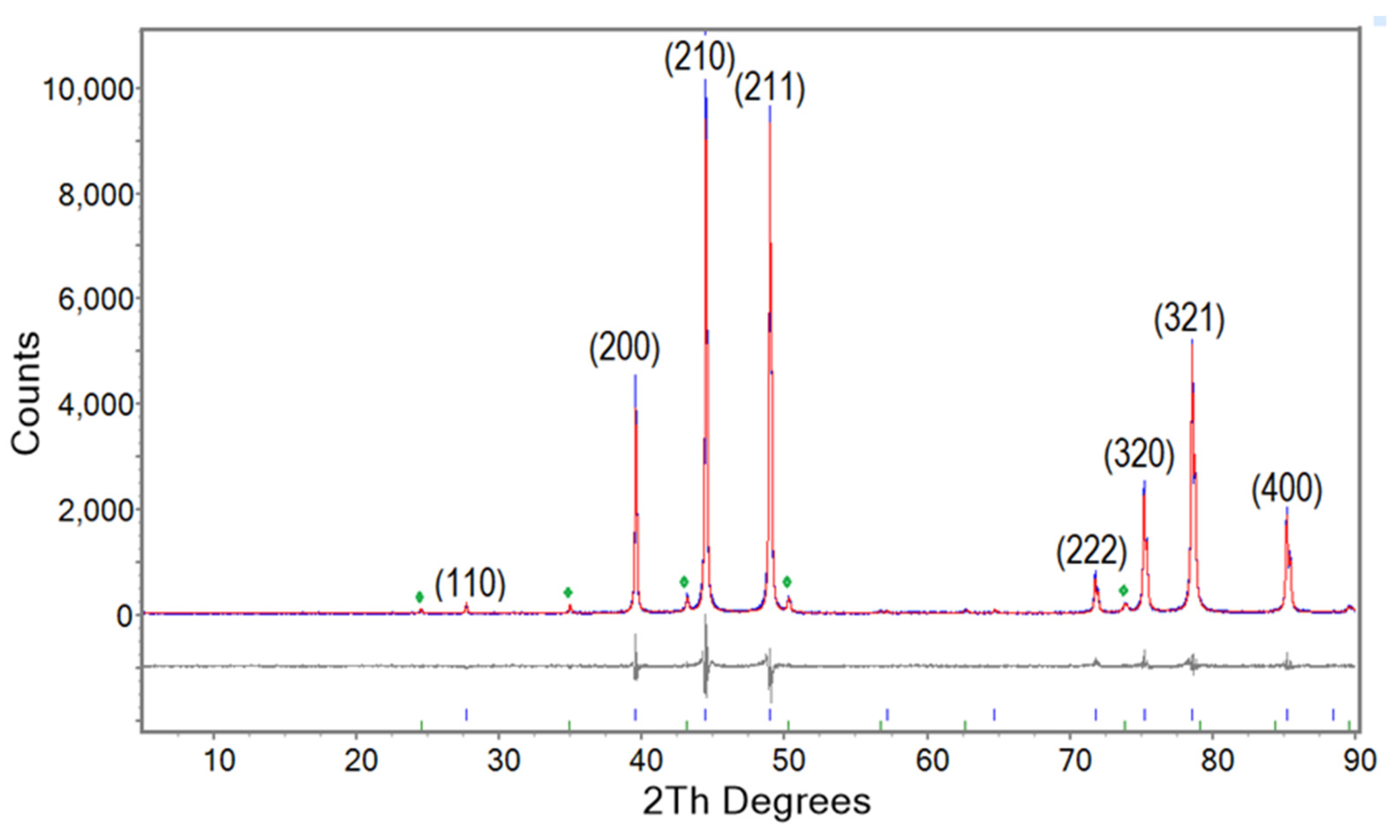
Figure 2.
EBSD phase maps of Nb1−βSnβ aggregates showing (a) NS-1000/60 (Run 1), (b) NS-1000/60/arc (Run 2), (c) NS-720/105/arc/ann/900/3 (Run 6), (d) NS-1000/60/arc/ann/1000/60 (Run 3), (e) High magnification EBSD phase map of small black areas for NS-1000/60/arc/ann/1000/60. The white arrows in Figure 2(a) denote holes in NS-1000/60. Colour scheme matches the compound legend below (c): Nb3Sn—blue; NbO—red; Nb—green; Sn—yellow.
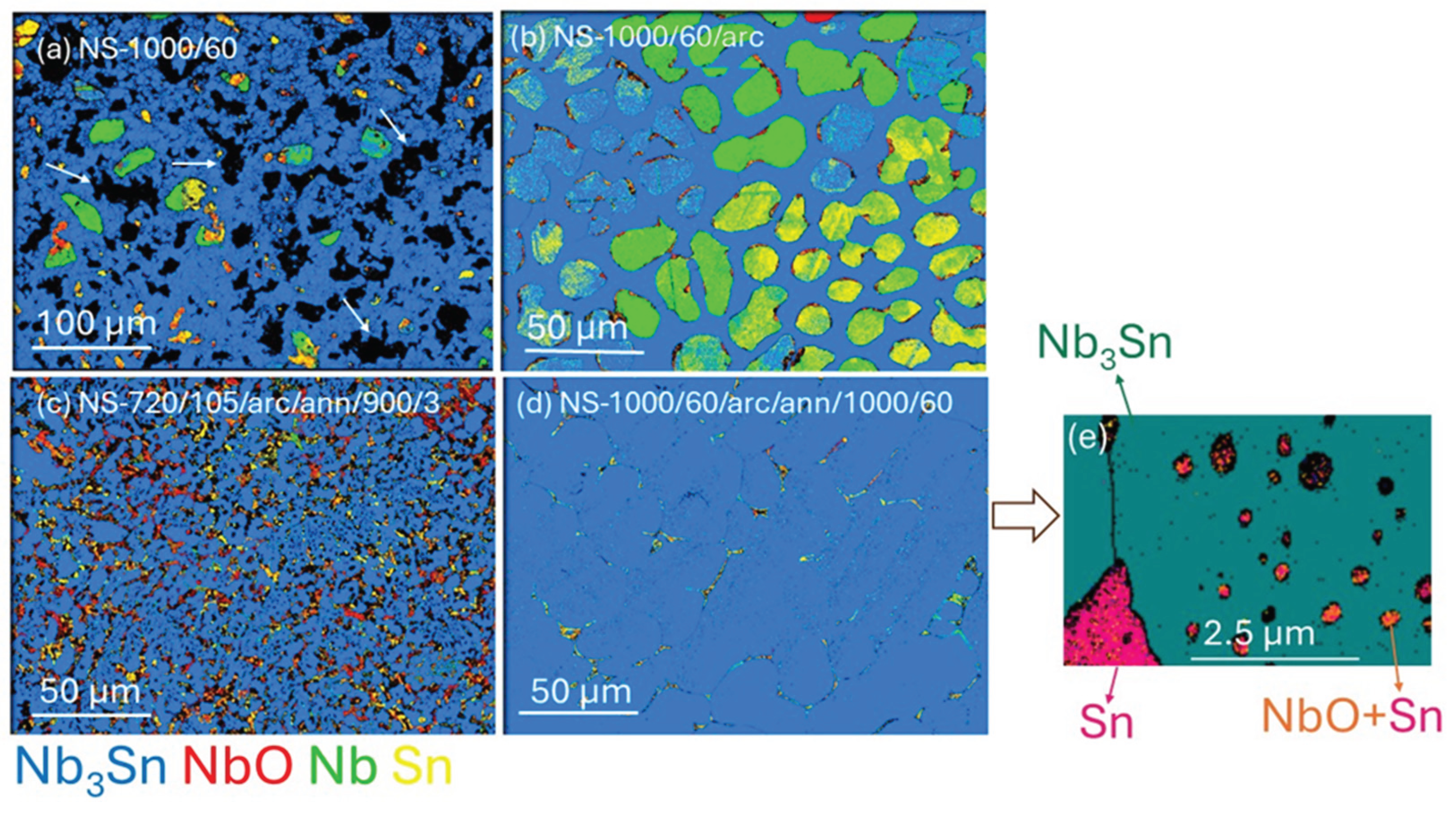
Figure 3.
Euler maps of (a) NS-1000/60 (Run 1), (b) NS-1000/60/arc, (Run 2), (c) NS-720/105/arc/ann/900/3 (Run 6), (d) NS-1000/60/arc/ann/1000/60 (Run 3). Euler angles are characterized by rotation of φ1 about the z-axis (red), rotation of φ about the rotated x-axis (green) and rotation φ2 about the y-axis (blue).
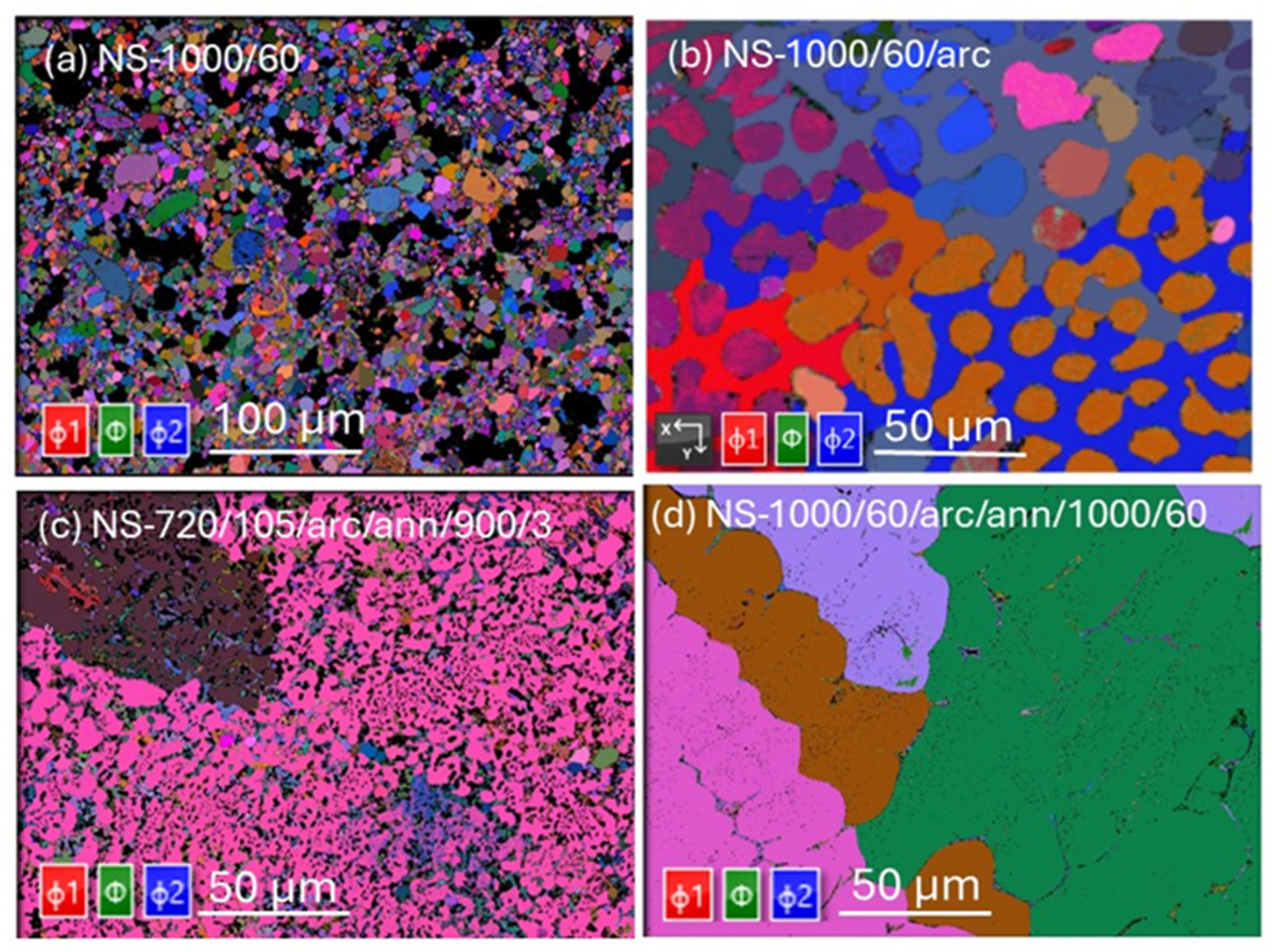
Figure 4.
Backscattered electron images of (a) NS-1000/60 (Run 1), (b) NS-1000/60/arc (Run2), (c) NS-720/105/arc/ann/900/3 (Run 6) and (d) NS-1000/60/arc/ann/1000/60 (Run 3). The white arrows denote holes, Nb-rich and Sn-rich areas. Red circles indicate locations of spot analyses using the EPMA.
Figure 4.
Backscattered electron images of (a) NS-1000/60 (Run 1), (b) NS-1000/60/arc (Run2), (c) NS-720/105/arc/ann/900/3 (Run 6) and (d) NS-1000/60/arc/ann/1000/60 (Run 3). The white arrows denote holes, Nb-rich and Sn-rich areas. Red circles indicate locations of spot analyses using the EPMA.
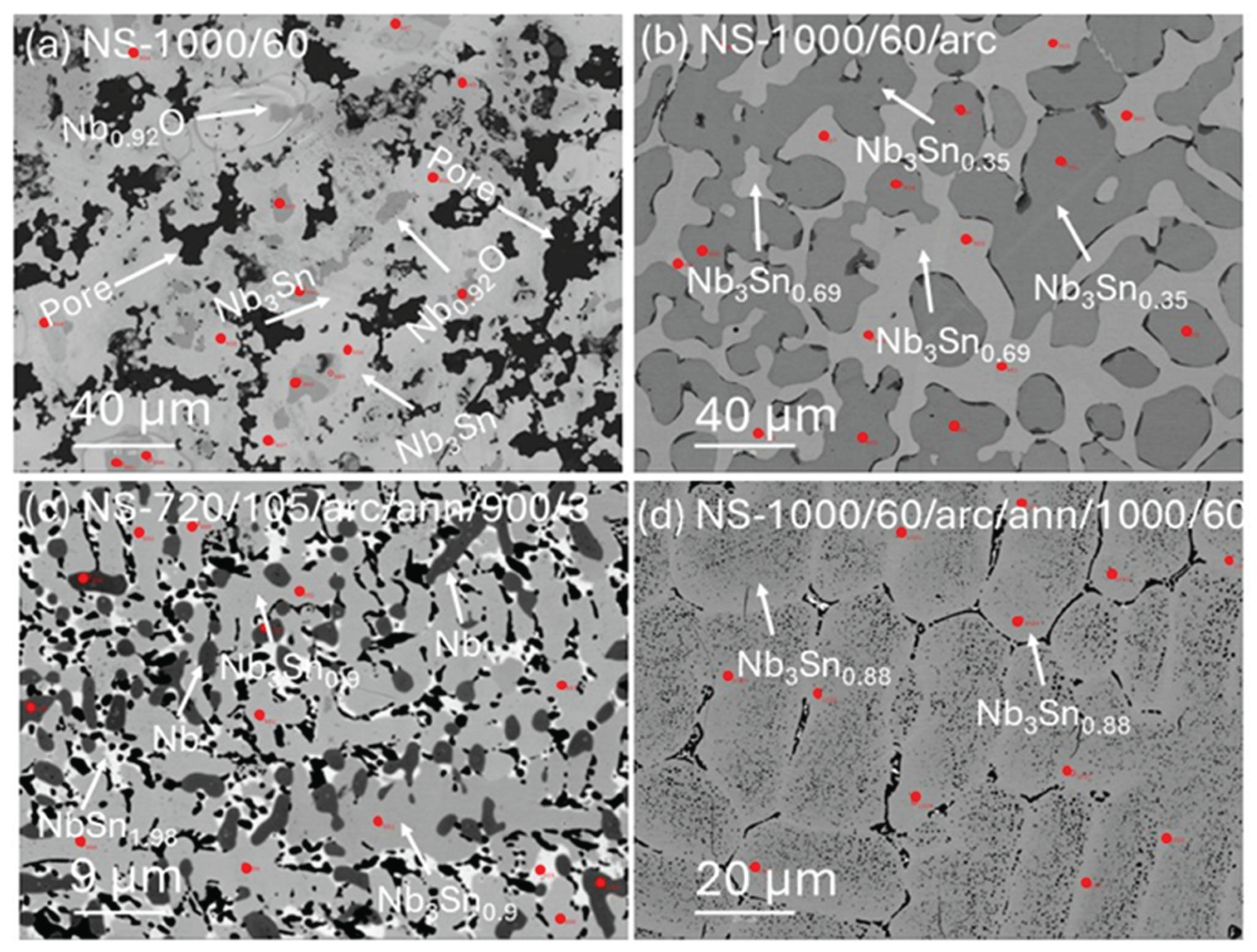
Figure 5.
(a) ZFC magnetization of Nb3Sn from NS-1000 (blue), NS-1000/60/arc (orange) NS-720/105/arc/ann/900/3 (maroon), NS-1000/60/arc/ann/1000/60 (green) and (b) critical current density of the same Nb3Sn samples as a function of an applied magnetic field at 10 K.
Figure 5.
(a) ZFC magnetization of Nb3Sn from NS-1000 (blue), NS-1000/60/arc (orange) NS-720/105/arc/ann/900/3 (maroon), NS-1000/60/arc/ann/1000/60 (green) and (b) critical current density of the same Nb3Sn samples as a function of an applied magnetic field at 10 K.
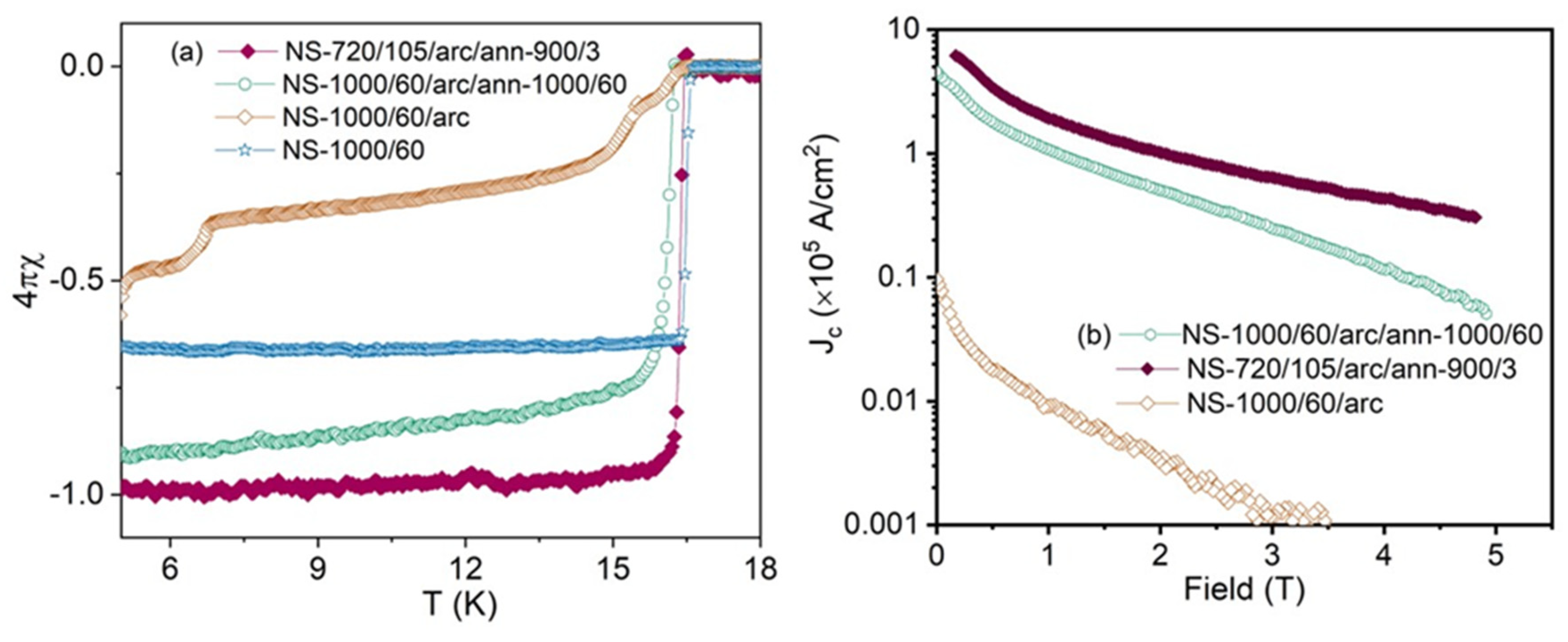
Figure 6.
Temperature dependence of resistance for (a) NS-720/105/arc/ann/900/3 (Run 6) and (b) NS-1000/60/arc/ann/1000/60 (Run 3) under different magnetic fields up to 5 T. (c) Hc2 (closed symbol) and Hirr (open symbol) versus temperature for NS-720/105/arc/ann/900/3 (green) and NS-1000/60/arc/ann/1000/60 (orange).
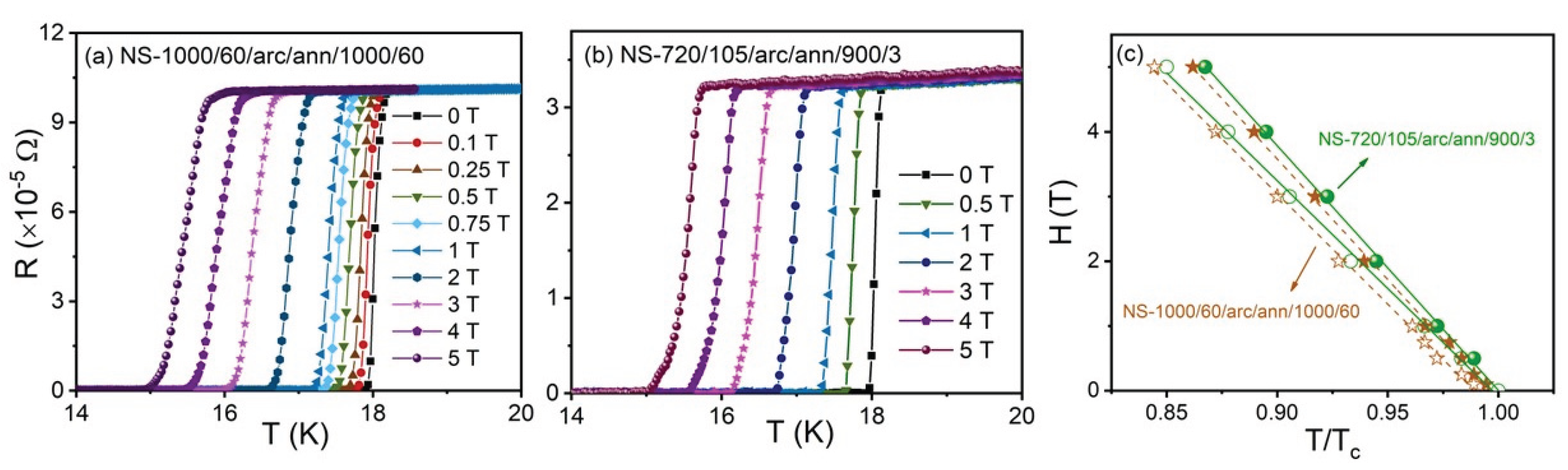
Figure 7.
Refined cell dimensions plotted against Sn content for Nb1−βSnβ samples listed in Table 3 (red diamonds). Linear plots for Nb1−βSnβ obtained by other studies ([8] blue solid line; [9] cyan dotted line); The trajectory by [8] is preferred by Goedeke [5]. Estimated standard errors for data from this study are within the symbol size. Note the statistically equivalent number of compositions for samples from Run 3 which straddle the trajectories determined by Devantnay et al. [8] and Flükiger et al. [9]. Adapted with permission from Figure 3 of Goedeke [5].
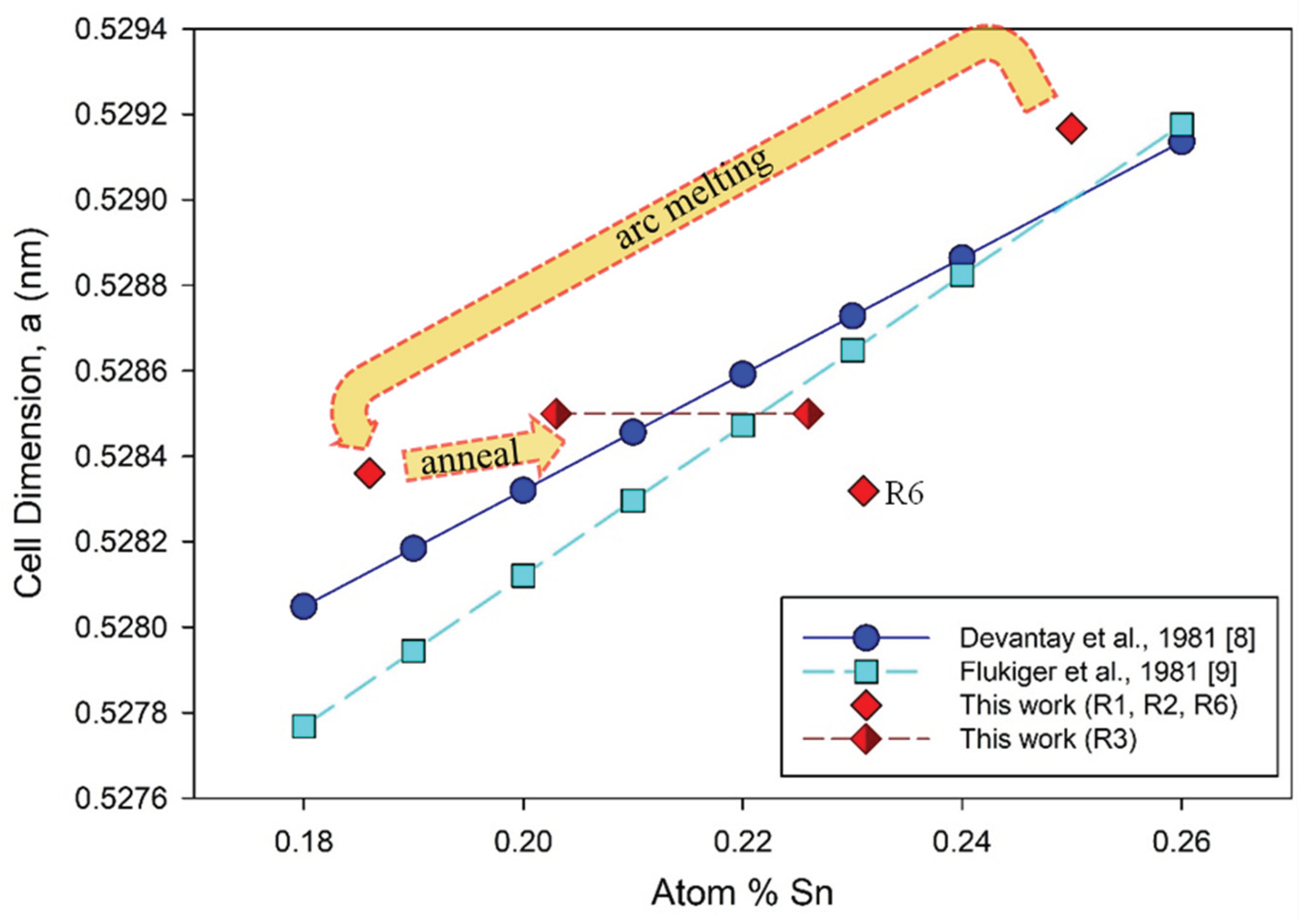

Table 1.
Sample ID, synthesis technique and heat treatment conditions for Nb3Sn samples.
| Run | Sample ID | Sintering condition |
Arc-melt | Post arc-melt Heat treatment |
| 1 | NS-1000/60 | 1000 oC/60 h | No | No |
| 2 | NS-1000/60/arc | 1000 oC/60 h | Yes | No |
| 3 | NS-1000/60/arc/ann/1000/60 | 1000 oC/60 h | Yes | 1000 oC/60h |
| 4 | NS-720/105 | 720 oC/105 h | No | No |
| 5 | NS-720/105/arc | 720 oC/105 h | Yes | No |
| 6 | NS-720/105/arc/ann/900/3 | 720 oC/105 h | Yes | 900 oC/3h |
Table 2.
Relative phase proportions and lattice parameters determined by Rietveld refinements.
| Run | Sample ID | Nb3Sn (%) | NbO (%) | Nb (%) | Unit Cell* (Å) | Rwp (%) | gof |
| 1 | NS-1000/60 | 94.69 | 3.57 | 1.74 | 5.29167(3) | 13.8 | 1.5 |
| 2 | NS-1000/60/arc | 85.16 | 4.80 | 10.04 | 5.28360(5) | 13.5 | 1.6 |
| 3 | NS-1000/60/arc/ann/1000/60 | 94.88 | 5.12 | - | 5.28510(4) | 12.2 | 1.5 |
| 6 | NS-720/105/arc/ann/900/3 | 85.99 | 3.49 | 10.52 | 5.28318(6) | 12.5 | 1.2 |
*Estimated standard deviation in parentheses.
Table 3.
Average compositions of selected grains in Nb–Sn samples determined by EPMA.
| Sample | n+ | Element atom % | Totals (wt%) | Stoichiometry | |||||
| Nb | Sn | O | Total | Nb | Sn | O | |||
| NS-1000/60 (R1) | |||||||||
| Nb3Sn1.00 | 21 | 75.0(2) | 25.0(2) | - | 100 | 98.7(4) | 3 | 1.00(1) | - |
| Nb0.92O | 9 | 47.9(7) | - | 52.1(7)* | 100 | 100 | 0.92 | - | 1 |
| Nb | 5 | 100.0 | - | - | 100 | 1 | - | - | |
| NS-1000/60/arc (R2) | |||||||||
| Nb3Sn0.69 | 20 | 81.4(1) | 18.6(1) | - | 100 | 99.6(3) | 3 | 0.69(1) | - |
| Nb3Sn0.35 | 20 | 89.6(2) | 10.4(2) | - | 100 | 99.5(2) | 3 | 0.35(1) | - |
| NS-1000/60/arc/ann/1000/60 (R3) | |||||||||
| Nb3Sn0.88 | 9 | 77.4(6) | 22.6(6) | - | 100 | 99.8(2) | 3 | 0.88(3) | - |
| Nb3Sn0.77 | 10 | 79.7(4) | 20.3(4) | - | 100 | 99.7(3) | 3 | 0.77(2) | - |
| NS-720/105/arc/ann/900/3 (R6) | |||||||||
| Nb3Sn0.90 | 21 | 76.9(3) | 23.1(3) | - | 100 | 99.8(2) | 3 | 0.90(2) | - |
| Nb1Sn1.98 | 5 | 33.6(4) | 66.4 (4) | - | 100 | 98.7(4) | 1 | 1.98(3) | - |
*Oxygen calculated by difference from 100; +n is the number of point analyses used to obtain average composition; values in parentheses are for one standard deviation. Weight percentage totals provide an indication of analytical precision.
Table 4.
Calculated Tc versus measured Tc for different concentrations of Sn in Nb1-βSnβ.
| Sn (at %) (calc) [22] | Tc (K) (calc) [22] | Tc (K) (experiment) [22] |
Sn (at %) (this work) |
Tc (K) (this work) |
| 18.75 | 9.2 | 6 | 18.60 | 6.78* |
| 20.83 | 11.3 | 9.5 | 22.59 | 16.26* |
| 23.44 | 16.1 | 16 | 23.09 | 16.45* |
| 25.00 | 18.2 | 18 | 25.02 | 16.58* |
*Tc obtained from ZFC and FC measurements.
Disclaimer/Publisher’s Note: The statements, opinions and data contained in all publications are solely those of the individual author(s) and contributor(s) and not of MDPI and/or the editor(s). MDPI and/or the editor(s) disclaim responsibility for any injury to people or property resulting from any ideas, methods, instructions or products referred to in the content. |
© 2025 by the authors. Licensee MDPI, Basel, Switzerland. This article is an open access article distributed under the terms and conditions of the Creative Commons Attribution (CC BY) license (https://creativecommons.org/licenses/by/4.0/).
Copyright: This open access article is published under a Creative Commons CC BY 4.0 license, which permit the free download, distribution, and reuse, provided that the author and preprint are cited in any reuse.


