Submitted:
24 June 2025
Posted:
26 June 2025
You are already at the latest version
Abstract
High-reliability electronics demand full-coverage verification of component integrity, yet conventional inspection methods remain limited in scope and unable to detect subtle or undocumented modifications. This work presents a secure hardware assurance framework that leverages visual AI, specifically deep learning applied to high-resolution images from Automated Optical Inspection (AOI) systems, to detect component-level anomalies in printed circuit board assemblies (PCBAs). The modular system integrates object detection, semantic segmentation, and a second-stage anomaly classifier, enabling detection of unauthorized modifications, substitutions, and structural deviations with high precision. Trained using a bootstrapped procedure on multi-domain datasets, including clean production boards and degraded scrap units, the model generalizes across real-world conditions with over 99% detection accuracy and sub-second board-level analysis times. In light of recent hardware-level cyber threats, such as the discovery of rogue communication devices embedded in commercial infrastructure, the need for scalable, image-based verification has never been more critical. This method transforms existing AOI data into an intelligent layer of visual forensics, enabling manufacturers to detect covert hardware changes and enforce trust in deployed electronic systems.
Keywords:
visual inspection
; anomaly detection
; secure hardware assurance
; deep learning
; automated optical inspection (AOI)
; component authentication
; PCB assembly
; counterfeit detection
; manufacturing integrity
; hardware cybersecurity
1. Introduction
The reliability and security of modern electronic systems are increasingly challenged by component-level anomalies, including counterfeit parts, unauthorized modifications, and assembly inconsistencies[1,2,3]. These issues are particularly critical in domains such as aerospace, medical, energy infrastructure, and defense electronics, where undetected deviations can have severe functional or national security implications[4]. Although automated optical inspection (AOI) systems are standard in electronics manufacturing, their capabilities are largely limited to rule-based checks for component presence or orientation, leaving more subtle, security-relevant issues undetected [5,6,7,8,9].
Recent advances in deep learning and pattern recognition offer new opportunities to enhance visual inspection using AOI-generated images[10,11,12,13,14,15]. These high-resolution images, which are already captured during manufacturing, can serve as a valuable source of structured data for detecting anomalies based on shape, marking consistency, placement geometry, and surface features. However, traditional AOI systems do not leverage this potential due to their reliance on static rules and limited image interpretation.
The need for secure hardware assurance has become increasingly urgent in light of recent revelations concerning supply chain vulnerabilities. A May 2025 investigative report by Reuters revealed that rogue communication devices, undocumented wireless modules, were discovered embedded in Chinese-manufactured solar inverters deployed across U.S. infrastructure [16]. These components, not listed in the product documentation, enabled covert remote access and bypassed existing cybersecurity protections. This incident underscores the critical gap between software-level defenses and the physical verification of hardware, especially when undocumented modifications remain invisible to conventional traceability and inspection tools. A related and widely publicized example is the “Big Hack,” in which printed circuit board assemblies (PCBAs) were allegedly implanted with rogue components to facilitate cyber-espionage against infrastructure and government-controlled systems [3]. Together, these incidents illustrate the need for systematic, scalable, and intelligent methods to verify the physical integrity of hardware—beyond what rule-based inspection or supply chain documentation alone can provide.
This paper presents a deep learning–based visual inspection framework that applies object detection and segmentation models to AOI image data. The system learns expected visual and spatial patterns from reference board assemblies and identifies deviations indicative of tampering, component substitution, rework, or contamination. We evaluate the performance of this framework across production-grade and degraded board conditions and demonstrate its ability to detect security-relevant anomalies with high precision and low false-positive rates. By enabling scalable, image-based verification of electronic assemblies, this approach contributes a critical layer to secure hardware assurance frameworks. To enable fast and accurate detection of components under varying imaging conditions, the framework employs the YOLOv12 architecture, a real-time object detector known for its high precision and robustness in dense visual scenes [17,18,19,20]. Its capability to balance inference speed and detection accuracy makes it suitable for high-resolution AOI imagery in electronics manufacturing.
1.1. Limitations of Existing Inspection Practices
Despite the growing importance of hardware assurance, current industry practices rely heavily on indirect or partial verification methods. Traceability protocols such as IPC-1782 or NIST's cybersecurity frameworks focus on documenting supply chain events but do not validate the actual components assembled on the board[21,22,23,24]. In many cases, visual or electrical inspection is performed on a sample basis only, [11,25]leaving the majority of components unchecked and vulnerable to undetected substitution, mislabelling, or tampering.
Physical inspection methods such as X-ray imaging and electrical testing are both expensive and impractical for real-time inspection in high-volume environments [26]. Moreover, they often fail to detect surface-level visual anomalies that may indicate subtle forms of rework or component fraud. Trusted supplier agreements reduce but do not eliminate risk, particularly when rework or substitution occurs after initial sourcing, during manufacturing, or in logistics.
Given these constraints, there is a pressing need for a full-coverage, image-based verification strategy that can operate automatically, scalably, and with minimal production disruption. The approach proposed in this work transforms underutilized AOI imaging data into a foundation for deep learning–based inspection, enabling the identification of visual anomalies at the component level with precision previously unattainable in standard production environments.
1.2. Contributions
This work makes the following contributions:
- Proposes a scalable and non-invasive framework for secure hardware assurance using deep learning on AOI imagery.
- Integrates YOLOv12-based object detection with semantic segmentation to enable fine-grained component-level analysis.
- Introduces a bootstrapped training strategy that generalizes across pristine, degraded, and field-recovered board images.
- Demonstrates real-world applicability by detecting unauthorized modifications, substitutions, and tampering events in production PCBAs.
- Achieves over 99% anomaly detection accuracy with sub-second inference times, enabling deployment in high-throughput environments.
2. Method
The proposed inspection framework is designed to analyze high-resolution images generated by Automated Optical Inspection (AOI) systems, enabling component-level verification and anomaly detection through deep learning. It integrates two core capabilities: object detection for identifying and localizing all components on a board, and semantic segmentation[27] for detailed analysis of component geometry and solder interfaces. Together, these models enable visual fingerprinting and structural validation, allowing the system to detect deviations from reference board designs caused by tampering, substitution, or untracked rework[10,11,25,28]. The overall workflow, including dataset preparation, model training, and anomaly detection, is illustrated in Figure 1.
2.1. Limitations of Existing Inspection Practices
The system operates on image datasets acquired from inline AOI systems or high-resolution post-production scanners. The primary dataset consists of clean, high-contrast images from boards captured in production environments under controlled lighting and camera conditions. These images serve as the training baseline for learning spatial layouts and component shapes. To ensure robustness, additional datasets were created from scrap boards collected at recycling centers. These boards were imaged both in cleaned (lightly dusted and washed) and uncleaned (oxidized, damaged) states, capturing realistic visual variability such as corrosion, surface wear, and foreign material presence.
This multi-domain dataset supports model generalization across pristine, degraded, and field-recovered board conditions, critical for real-world deployment where production variability and contamination are common.
2.2. Object Detection
We use the YOLOv12 architecture for component-level object detection [29]. This architecture was selected due to its balance between inference speed and accuracy, which is essential for analyzing densely populated AOI images of electronic assemblies. YOLOv12’s performance on small objects, combined with its robustness to noise and partial occlusion, makes it effective in real-world PCB conditions. Paired with semantic segmentation, which enables pixel-level analysis of solder pad integrity and component outlines, the framework captures both layout-level and fine-grained geometric anomalies. This modular combination offers significantly greater flexibility and detection depth than a monolithic end-to-end approach.
The model is trained to localize all visible components on a board and classify them by package type. Initial training is conducted on images from pristine AOI datasets, using CAD-aligned bounding boxes for supervision. To improve generalization, a bootstrapping procedure is used: the model is applied to images from the degraded datasets, predictions are manually corrected, and the network is retrained iteratively [30,31,32].
The YOLOv12 model was trained with a batch size of 16, using the Adam optimizer and an initial learning rate of 0.001. Input images were resized to 640 × 640 pixels, and training spanned 360 epochs. Data augmentation techniques included horizontal and vertical flipping, random brightness shifts, rotation (±15°), and Gaussian blur to simulate real-world variability.
During the bootstrapping process, the model trained on pristine boards is applied to degraded and noisy datasets. Predictions with low confidence or incorrect localization are manually reviewed and corrected to generate new labeled samples. These corrected samples are then added to the training set, and the model is retrained. This iterative loop is repeated until performance stabilizes across board conditions. The bootstrapping cycle functions as a self-improving mechanism that incrementally enhances the model’s ability to handle low-contrast, contaminated, or structurally damaged boards, conditions under which rule-based inspection often fails.
This approach allows the detection model to maintain high accuracy even in low-contrast, noisy, or partially damaged conditions. Detection outputs include bounding box coordinates, confidence scores, and component class labels, which are used downstream for structural consistency checks and anomaly filtering. An example of the model's output on a production-grade board is shown in Figure 2.
2.3. Component Segmentation
In parallel to detection, we apply a semantic segmentation model trained to isolate each component’s body and solder pad regions. This segmentation enables pixel-level analysis of shape, orientation, and solder coverage, features critical for identifying unauthorized modifications or quality issues such as rework or improper mounting.
Segmentation training uses high-resolution AOI images annotated with masks for each component and pad. As with detection, a bootstrapping workflow is employed to extend training across degraded boards. The model achieves high precision and recall on both clean and noisy datasets, supporting robust feature extraction for downstream comparison. Figure 3 illustrates the output of the segmentation model, showing distinct masks for the component body and pad regions.
Segmented component shapes are compared to a reference models, enabling bottom-up visual fingerprinting and detection of anomalies such as footprint mismatch, lead deformation, missing pads, or suspicious markings.
2.4. Anomaly Detection Pipeline
The final stage of the framework integrates detection and segmentation results to identify structural or visual anomalies. Detected components are first validated against expected layouts using geometric and spatial analysis. A learned model of layout tolerance, captured from 20 to 100 reference boards, accounts for typical manufacturing variation while highlighting deviations such as missing, added, or swapped components.
Each detected anomaly is then classified by a second-stage AI module that evaluates severity and type (e.g., missing, extra, piggybacked, rotated, or contaminated). This second-stage module is implemented as a shallow convolutional neural network (CNN) with three convolutional layers followed by a fully connected classifier. It receives a feature vector derived from the output of the detection and segmentation stages, including component geometry (bounding box dimensions, pad shape), relative position, surface texture descriptors, and mask alignment scores. The classifier assigns the anomaly to one of several predefined categories: missing, added, rotated, piggybacked, contaminated, unknown, or reworked. This modular design allows anomaly severity and type to be evaluated independently from detection confidence, and supports downstream filtering or alerting based on context. Thresholds can be configured by the user to tune sensitivity for specific use cases or board classes.
The method incorporates several safeguards for handling uncertain or degraded inputs. Predictions with confidence below a configurable threshold are excluded from anomaly evaluation or flagged for manual review, reducing false positives. Spatial outliers are detected using learned tolerances derived from reference layouts, which account for typical placement variation but flag large deviations. In cases where a component is missing or heavily occluded, anomaly scores are suppressed unless corroborated by layout analysis or segmentation failure.
This layered architecture enables the system to distinguish between benign visual noise and security-relevant anomalies, delivering precise and scalable verification suitable for both production QA and post-deployment forensics.
2.5. Framework Overview
The proposed inspection system operates as a multi-stage pipeline that integrates object detection, semantic segmentation, and anomaly classification into a cohesive framework. The process begins with the acquisition of high-resolution AOI images from both clean and degraded printed circuit boards. These images are first processed by a YOLOv12-based object detection model, which localizes all visible components and classifies them by package type.
The output bounding boxes and class labels are then used to guide a semantic segmentation model, which extracts pixel-level masks of the component body and solder pads. These masks are compared to golden references for geometric consistency and alignment. Combined features from detection and segmentation are passed to a second-stage classifier that evaluates deviations and determines anomaly type and severity. This architecture allows for both structural validation and security anomaly detection, enabling inspection under a wide range of conditions. The end-to-end pipeline is illustrated in Figure 1.
3. Experimental Results and Case Studies
To validate the proposed AOI image–based inspection framework, we conducted a series of experiments on diverse datasets representing both production-grade and degraded board conditions. The evaluation focuses on detection accuracy, segmentation quality, anomaly classification, and overall robustness across different visual environments. Additionally, we include case studies that demonstrate the framework’s ability to detect genuine tampering, component substitution, and undocumented rework events in real-world PCB assemblies.
3.1. Evaluation of Detection and Segmentation Models
The object detection model, based on YOLOv12, was trained using three datasets:
- Clean AOI images from production environments aligned with CAD data,
- Cleaned scrap boards scanned under controlled conditions, and
- Uncleaned scrap boards representing worst-case scenarios including oxidation, broken components, and noise.
Training followed a staged bootstrapping strategy, progressing from pristine to degraded datasets. The model’s convergence behavior over 360 epochs is illustrated in Figure 4, which presents combined and individual loss curves, as well as validation dynamics and inter-loss correlations.
Performance on unseen test boards is summarized in Table I. The model achieved an F1 score of 0.96 on pristine boards, 0.92 on cleaned scrap boards, and 0.82 on degraded scrap boards, with an overall average of 0.90. Precision and recall remained consistently high across all conditions, confirming the model’s robustness.
Table I. score, precision, and recall for three test board types: pristine, cleaned scrap, and dirty scrap boards.[x].

| Board Condition | F1 Score | Precision | Recall |
|---|---|---|---|
| Pristine AOI Image | 0.96 | 0.96 | 0.96 |
| Clean Scrap Board | 0.92 | 0.89 | 0.96 |
| Dirty Scrap Board | 0.82 | 0.78 | 0.89 |
| Average | 0.90 | 0.88 | 93.7 |
These results demonstrate the model's resilience under diverse conditions. While performance on pristine boards reached an F1 score of 0.96, the drop to 0.82 on dirty scrap boards reflects the expected impact of visual degradation, yet still maintains acceptable detection performance for operational use. Importantly, the low variance in recall (±0.07 across board types) confirms the model's ability to consistently identify components, even when appearance is compromised. Compared to typical rule-based AOI systems, which often fail to detect over 40% of anomalies on degraded boards, the deep learning–based approach reduces false negatives substantially while maintaining low false positive rates. The segmentation model was evaluated on 2,371 component instances from 241 images. Using separate masks for body and pad regions, the model achieved a mean average precision (mAP50) of 96.9%, with class-specific precision exceeding 0.91 for bodies and 0.97 for pads, as reported in Table II.
Table II. scores for segmentation of component bodies and solder pads. Results demonstrate strong pixel-level localization capabilities, even under visual degradation.
| Class | Precision | Recall | mAP50 |
|---|---|---|---|
| Body | 0.911 | 0.919 | 0.961 |
| Pad | 0.975 | 0.934 | 0.978 |
| All | 0.943 | 0.927 | 0.969 |
The segmentation model achieves strong pixel-level precision, particularly on pad regions, which are critical for detecting footprint mismatch. High mAP50 scores for both classes indicate consistent boundary accuracy, essential for downstream anomaly classification. The segmentation model’s performance across varying confidence thresholds is shown in Figure 5. It maintains high reliability and consistent behavior, making it suitable for fine-grained structural verification.
These detection and segmentation results form the core of the anomaly detection pipeline. Their ability to generalize across board quality and environmental conditions ensures effective performance in real-world manufacturing and field-inspection scenarios.
3.2. Real-World Detection Case Studies
The framework was deployed on real-world production datasets to evaluate its effectiveness in detecting unauthorized modifications and undocumented deviations from design specifications. These case studies highlight scenarios where conventional traceability and rule-based inspection would fail to detect critical anomalies.
In one case, the system flagged a microcontroller due to inconsistent markings compared to the approved bill of materials. Visual comparison revealed that the component originated from a different manufacturer, despite matching electrical specifications. The discrepancy, confirmed through image-based fingerprinting, illustrated the system’s capability to detect unapproved substitutions invisible to traceability logs.
In another case, a passive component logged as Panasonic was identified visually as a Vishay part. Differences in package geometry and surface finish were detected through both object classification and segmentation. This mismatch, caused by a supplier labeling error, would not have been caught by traditional inspection methods.
A third case involved a component logged as a Bourns device but which could not be matched to any known reference in the golden dataset. The visual fingerprint failed classification, and the system flagged the part as an unknown. Manual investigation confirmed it to be an unauthorized or counterfeit component.
The system also demonstrated its ability to detect layout-level anomalies. As shown in Figure 5, top-side inspection identified boards with missing, added, and swapped components relative to the learned reference layout.
Visual inspection also revealed cases of hardware tampering techniques such as piggybacking, where an unauthorized component is soldered atop an approved one. This covert alteration, shown in Figure 7, bypassed standard AOI systems but was identified by the anomaly classifier.
Another notable case involved the post-production addition of a wire between two points on a board—an undocumented modification likely intended to override circuit behavior or enable a backdoor function. Figure 8 illustrates this anomaly, captured and flagged by the system.
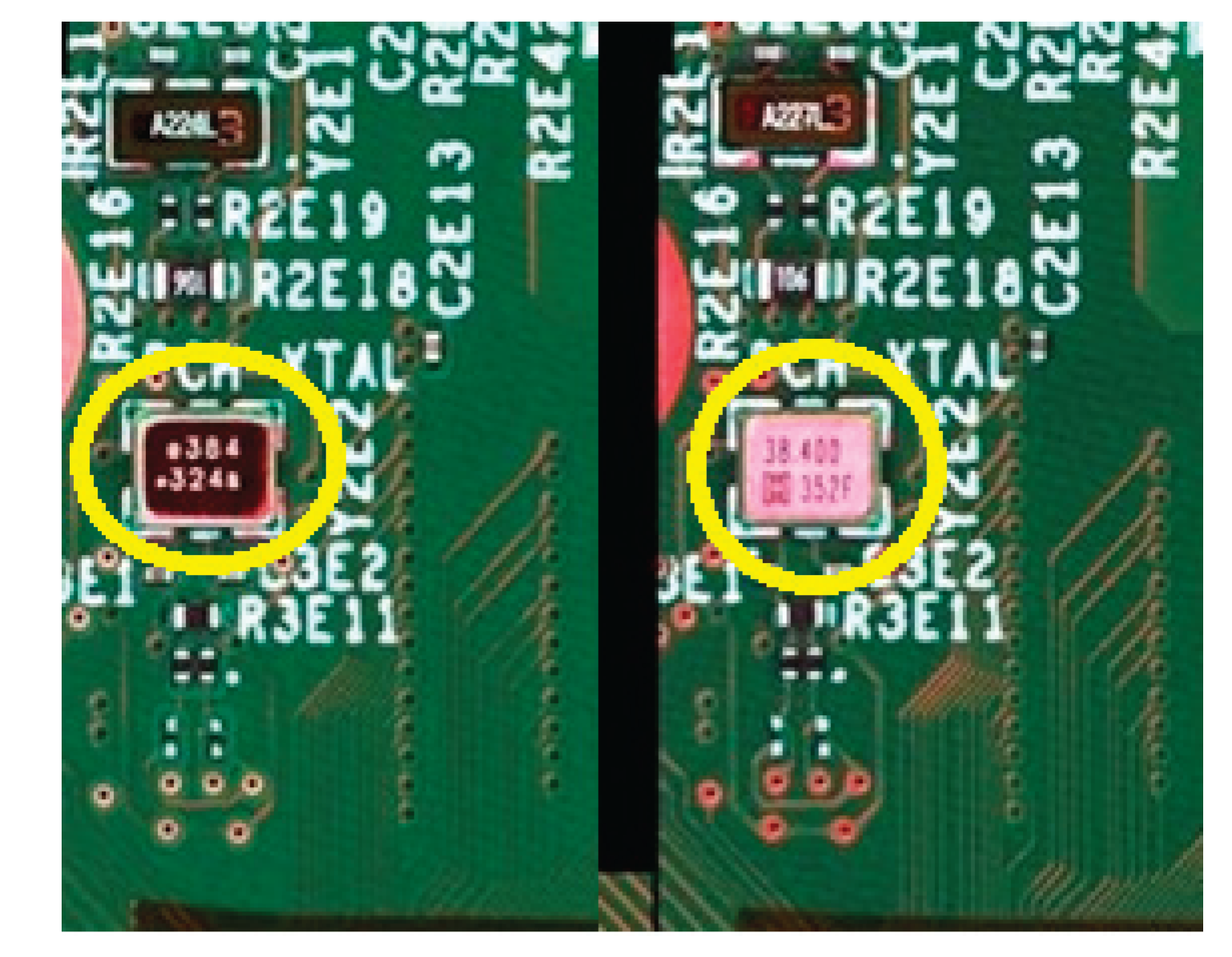
A representative example is shown in Figure 9, where a crystal oscillator was substituted with a visually similar part from a different manufacturer. Though electrically equivalent, the system detected discrepancies in marking, pad layout, and surface finish, triggering an anomaly alert.
3.3. Scalability and Throughput
The framework was benchmarked for processing performance on standard AOI image resolutions. The detection pipeline processed images at <1000 ms per board, with component-level inferences running in under 10 ms per instance. This allows efficient post-production analysis of full board datasets without introducing bottlenecks to production workflows.
The method achieves:
- >99.3% anomaly detection accuracy
- <0.5% false positive rate
- <1% false negative rate
These metrics demonstrate the suitability of the framework for high-volume board analysis, enabling full coverage verification without reliance on manual inspection or destructive testing.
4. Discussion
The results demonstrate that deep learning models trained on AOI image data can achieve high accuracy in component detection, segmentation, and anomaly classification across diverse board conditions. Unlike traditional inspection techniques, which are often constrained by rule-based logic or sample-based strategies, the proposed framework provides data-driven, full-coverage inspection at the component level, using visual cues alone.
A key strength of the system lies in its ability to generalize across pristine, mildly degraded, and severely contaminated boards. This resilience is essential for real-world deployment, where imaging conditions, component aging, or handling artifacts may affect visual quality. The bootstrapping-based training pipeline, incorporating clean and field-grade boards, ensures that the model is robust to such variations, maintaining low false positive rates even under challenging conditions.
Importantly, the framework does not rely on electrical signals, traceability logs, or physical probing to detect anomalies. Instead, it leverages high-resolution imaging data already produced by AOI systems, making it non-invasive and readily integrable into existing manufacturing workflows. This enables scalable deployment without the need for additional hardware or inspection stations.
The anomaly detection pipeline also highlights a key benefit of combining object detection and segmentation. While detection provides spatial and classification data, segmentation enables pixel-level geometry analysis. Together, these allow for nuanced differentiation between normal variation and security-relevant modifications such as component substitution, piggybacking, or footprint mismatch.
While the performance metrics are strong, several limitations remain. First, the model depends on access to high-quality AOI images, which may vary by manufacturer and inspection system. Second, while the system can flag unknown components or mismatches, root cause analysis, such as determining whether a discrepancy is due to fraud, error, or rework, still requires human investigation. Finally, expanding the reference database of verified components and improving automated labeling of anomalies remain ongoing challenges for scaling the system across new product lines.
Despite these considerations, the approach marks a shift toward intelligent, vision-based quality and security assurance. By transforming AOI data into a rich source of structured information, manufacturers can move beyond static rules and manual inspection toward adaptive, AI-driven verification pipelines.
This methodology can also complement existing traceability and cybersecurity frameworks, providing visual evidence of component integrity and enhancing supply chain transparency. As electronic systems become increasingly interconnected and mission-critical, the ability to verify every board’s composition through image-based AI may become an essential tool in ensuring both quality and trust.
Several mitigation strategies can be pursued to address these limitations. Image quality variability could be reduced through domain adaptation techniques or contrast normalization methods, improving robustness across imaging environments. The reliance on human review for root cause analysis may be mitigated by incorporating explainable AI tools that provide interpretable anomaly features to assist operators. Additionally, expanding the reference database can be accelerated through semi-supervised labeling strategies or federated learning from multiple production sites, enabling rapid adaptation to new products without extensive manual annotation.
Unlike conventional rule-based AOI systems, which rely on pre-defined geometric tolerances and optical contrast thresholds, the proposed deep learning framework learns visual patterns and contextual relationships directly from data. This allows it to detect anomalies that fall outside the scope of rule definitions, such as unauthorized but electrically equivalent component substitutions, surface-level tampering, or non-conforming rework. Rule-based systems typically suffer from high false negative rates in degraded or non-standard imaging conditions, whereas the presented approach maintains high detection accuracy even on visually compromised boards. Additionally, the ability to incorporate layout and marking consistency into the anomaly evaluation makes the proposed method more adaptable and resilient than static rule-based inspection engines.
This sufficiency stems from the system's ability to learn implicit patterns of legitimate component appearance, placement, and orientation across many examples, rather than relying on hand-crafted rules. The segmentation module enables pixel-level analysis of pad geometry and component shape, capturing nuances like surface finish, lead deformation, or non-standard mounting that rules cannot encode. By fusing these learned visual features with layout expectations, the system can robustly identify both gross and subtle anomalies, including those intentionally designed to evade rule-based detection. The result is a more comprehensive and context-aware inspection capability that adapts to variability without requiring reconfiguration.
5. Conclusion
This work presents a secure hardware assurance solution based on deep learning applied to AOI images of electronic assemblies. By integrating object detection, segmentation, and spatial anomaly classification, the system performs high-precision component-level verification without requiring electrical tests or destructive analysis. Trained across a diverse set of production and degraded boards, the framework generalizes well to real-world conditions and operates efficiently within high-throughput environments.
Unlike traditional inspection systems limited to rule-based validation or sample testing, this approach provides full-coverage verification using only existing imaging infrastructure. With over 99% anomaly detection accuracy and millisecond-scale inference times, it enables practical deployment at scale, enhancing quality control and elevating hardware trust.
Recent events, including the discovery of rogue communication modules embedded in solar inverters, have exposed the limitations of conventional traceability and underscored the urgency of verifying what is physically present on a board. The proposed visual AI framework addresses this gap by transforming AOI data into a tool for structural and provenance-level analysis.
By bridging manufacturing analytics with cybersecurity principles, this method lays the foundation for scalable, non-invasive, and intelligent assurance of hardware integrity, essential for safeguarding the global electronics supply chain against tampering, counterfeiting, and cyber-physical compromise.
The method’s architecture, combining YOLOv12-based detection, semantic segmentation, and a dedicated anomaly classifier, enables flexible, scalable inspection across diverse PCB layouts and conditions. The bootstrapped training procedure, leveraging both pristine and degraded boards, strengthens generalization and reliability in uncontrolled environments. These features make the approach not only accurate, but also resilient, capable of detecting both subtle production deviations and deliberate, unauthorized hardware changes that rule-based methods often miss.
Author Contributions
Conceptualization, methodology, investigation, software, validation, and original draft preparation: Eyal Weiss.
Funding
This research received no external funding.
Data Availability Statement
The data presented in this study are available on request from the corresponding author. The data are not publicly available due to commercial restrictions.
Acknowledgments
Some language editing support in the preparation of this manuscript was provided by AI-based tools (OpenAI ChatGPT). All scientific content and final decisions were made by the author.
Conflicts of Interest
Author Eyal Weiss was employed by the company Cybord.ai.
References
- Tehranipoor, M.M.; Guin, U.; Forte, D. Counterfeit Integrated Circuits. In Counterfeit Integrated Circuits; Springer, 2015; pp. 15–36.
- Report, a S. Counterfeit Parts : Increasing Awareness and Developing Countermeasures Counterfeit Parts : Increasing Awareness And. T 2011.
- Mehta, D.; Lu, H.; Paradis, O.P.; Mukhil, M.A.; Rahman, M.T.; Iskander, Y.; Chawla, P.; Woodard, D.L.; Tehranipoor, M.; Asadizanjani, N. The Big Hack Explained: Detection and Prevention of PCB Supply Chain Implants. ACM J Emerg Technol Comput Syst 2020, 16. [Google Scholar] [CrossRef]
- Representatives, H. DEFENSE SUPPLY CHAIN DOD Needs Complete Information on Single Sources of Supply to Proactively Manage the Risks. 2017.
- Reshadat, V.; Kapteijns, R.A.J.W. Improving the Performance of Automated Optical Inspection (AOI) Using Machine Learning Classifiers. In Proceedings of the 2021 International Conference on Data and Software Engineering (ICoDSE); IEEE, 2021; pp. 1–5.
- Meyer, L.; Josefsson, B.; Vrotsou, K.; Westin, C.; Lundberg, J. Evaluation of an AOI Mapping and Analysis Tool for the Identification of Visual Scan Pattern. In Proceedings of the 2021 Ieee/aiaa 40th digital avionics systems conference (dasc); IEEE; 2021; pp. 1–8. [Google Scholar]
- Tong, X.; Yu, Z.; Tian, X.; Ge, H.; Wang, X. Improving Accuracy of Automatic Optical Inspection with Machine Learning. Front Comput Sci 2022, 16, 1–12. [Google Scholar] [CrossRef]
- Ni, Y.-S.; Chen, W.-L.; Liu, Y.; Wu, M.-H.; Guo, J.-I. Optimizing Automated Optical Inspection: An Adaptive Fusion and Semi-Supervised Self-Learning Approach for Elevated Accuracy and Efficiency in Scenarios with Scarce Labeled Data. Sensors 2024, 24, 5737. [Google Scholar] [CrossRef] [PubMed]
- Chen, I.-C.; Hwang, R.-C.; Huang, H.-C. PCB Defect Detection Based on Deep Learning Algorithm. Processes 2023, 11, 775. [Google Scholar] [CrossRef]
- Weiss, E. Advancements in Electronic Component Assembly: Real-Time AI-Driven Inspection Techniques. Electronics (Basel) 2024, 13, 3707. [Google Scholar] [CrossRef]
- Weiss, E. Counterfeit Mitigation by In-Line Deep Visula Inspection Available online: http://iconnect007.uberflip.com/i/1440051-smt007-jan2022/87?
- Chennamma, H.R.; Madhushree, B. A Comprehensive Survey on Image Authentication for Tamper Detection with Localization. Multimed Tools Appl 2023, 82, 1873–1904. [Google Scholar] [CrossRef]
- Rahman, M.T.; Shi, Q.; Tajik, S.; Shen, H.; Woodard, D.L.; Tehranipoor, M.; Asadizanjani, N. Physical Inspection & Attacks: New Frontier in Hardware Security. In Proceedings of the 2018 IEEE 3rd International Verification and Security Workshop (IVSW); 2018; pp. 93–102. [Google Scholar]
- Vashistha, N.; Lu, H.; Shi, Q.; Woodard, D.L.; Asadizanjani, N.; Tehranipoor, M.M. Detecting Hardware Trojans Using Combined Self-Testing and Imaging. IEEE Transactions on Computer-Aided Design of Integrated Circuits and Systems 2022, 41, 1730–1743. [Google Scholar] [CrossRef]
- Vashistha, N.; Rahman, M.T.; Shen, H.; Woodard, D.L.; Asadizanjani, N.; Tehranipoor, M. Detecting Hardware Trojans Inserted by Untrusted Foundry Using Physical Inspection and Advanced Image Processing. Journal of Hardware and Systems Security 2018, 2, 333–344. [Google Scholar] [CrossRef]
- Sarah Mcfarlane Rogue Communication Devices Found in Chinese Solar Power Inverters. Reuters 2025.
- Li, Y.; Duan, Y.; Duan, L.; Xiang, W.; Wu, Q. YOLO-TL: A Tiny Object Segmentation Framework for Low Quality Medical Images. In Proceedings of the Medical Image Understanding and Analysis; Yap, M.H., Kendrick, C., Behera, A., Cootes, T., Zwiggelaar, R., Eds.; Springer Nature Switzerland: Cham, 2024; pp. 143–159. [Google Scholar]
- Song, X.; Wang, Y.; Li, C.; Song, L. WDC-YOLO: An Improved YOLO Model for Small Objects Oriented Printed Circuit Board Defect Detection. J Electron Imaging 2024, 33, 013051. [Google Scholar] [CrossRef]
- Hu, M.; Li, Z.; Yu, J.; Wan, X.; Tan, H.; Lin, Z. Efficient-Lightweight YOLO: Improving Small Object Detection in YOLO for Aerial Images. Sensors 2023, 23. [Google Scholar] [CrossRef] [PubMed]
- Li, Y.; Li, S.; Du, H.; Chen, L.; Zhang, D.; Li, Y. YOLO-ACN: Focusing on Small Target and Occluded Object Detection. IEEE Access 2020, 8, 227288–227303. [Google Scholar] [CrossRef]
- Razak, G.M.; Hendry, L.C.; Stevenson, M. Supply Chain Traceability: A Review of the Benefits and Its Relationship with Supply Chain Resilience. Production Planning and Control 2023, 34, 1114–1134. [Google Scholar] [CrossRef]
- Rosales, P. Traceability in the Electronics Manufacturing Industry. 2021.
- Schuitemaker, R.; Xu, X. Product Traceability in Manufacturing: A Technical Review. In Proceedings of the Procedia CIRP; Elsevier B.V., 2020; Vol. 93; pp. 700–705. [Google Scholar]
- Corallo, A.; Latino, M.E.; Menegoli, M.; Pontrandolfo, P. A Systematic Literature Review to Explore Traceability and Lifecycle Relationship. Int J Prod Res 2020, 58, 4789–4807. [Google Scholar] [CrossRef]
- Weiss, E. Electronic Components Provenance Assurance Through AI and Big Data in Assembly Processes. IEEE Trans Compon Packaging Manuf Technol 2024, 1–1. [Google Scholar] [CrossRef]
- Sarkar, T.S.; Maitra, S.; Chakraborty, A.; Saha, A.; Chowdhury, J.; Mukhopadhyay, D. X-Factor: Deep Learning-Based PCB Counterfeit Detection Using X-Ray CT Techniques for Hardware Assurance. In Proceedings of the Proceedings of the 21st ACM International Conference on Computing Frontiers: Workshops and Special Sessions.
- Yang, H.; Liu, Y.; Xia, T. Defect Detection Scheme of Pins for Aviation Connectors Based on Image Segmentation and Improved RESNET-50. Int J Image Graph 2024, 24, 2450011. [Google Scholar] [CrossRef]
- Weiss, E. Electronic Component Analytics and Traceability Available online: www.cybord.ai.
- Zhao, X.; Dou, X.; Zhang, G. An Image Processing Technique for Optimizing Industrial Defect Detection Using Dehazing Algorithms. PLoS One 2025, 20, e0322217. [Google Scholar] [CrossRef] [PubMed]
- Huang, L.; Zhang, C.; Zhang, H. Self-Adaptive Training: Bridging Supervised and Self-Supervised Learning. IEEE Trans Pattern Anal Mach Intell 2024, 46, 1362–1377. [Google Scholar] [CrossRef] [PubMed]
- Abdulrazzaq, M.M.; Ramaha, N.T.A.; Hameed, A.A.; Salman, M.; Yon, D.K.; Fitriyani, N.L.; Syafrudin, M.; Lee, S.W. Consequential Advancements of Self-Supervised Learning (SSL) in Deep Learning Contexts. Mathematics 2024, 12. [Google Scholar] [CrossRef]
- Grill, J.-B.; Strub, F.; Altché, F.; Tallec, C.; Richemond, P.H.; Buchatskaya, E.; Doersch, C.; Avila Pires, B.; Daniel Guo, Z.; Gheshlaghi Azar, M.; et al. Bootstrap Your Own Latent A New Approach to Self-Supervised Learning.
Figure 1.
Overview of the Inspection Framework Pipeline. The workflow includes acquisition of clean and scrap board datasets, initial training of YOLOv12 and segmentation models, bootstrapped retraining on degraded boards, and final anomaly detection based on detection and segmentation outputs.
Figure 1.
Overview of the Inspection Framework Pipeline. The workflow includes acquisition of clean and scrap board datasets, initial training of YOLOv12 and segmentation models, bootstrapped retraining on degraded boards, and final anomaly detection based on detection and segmentation outputs.
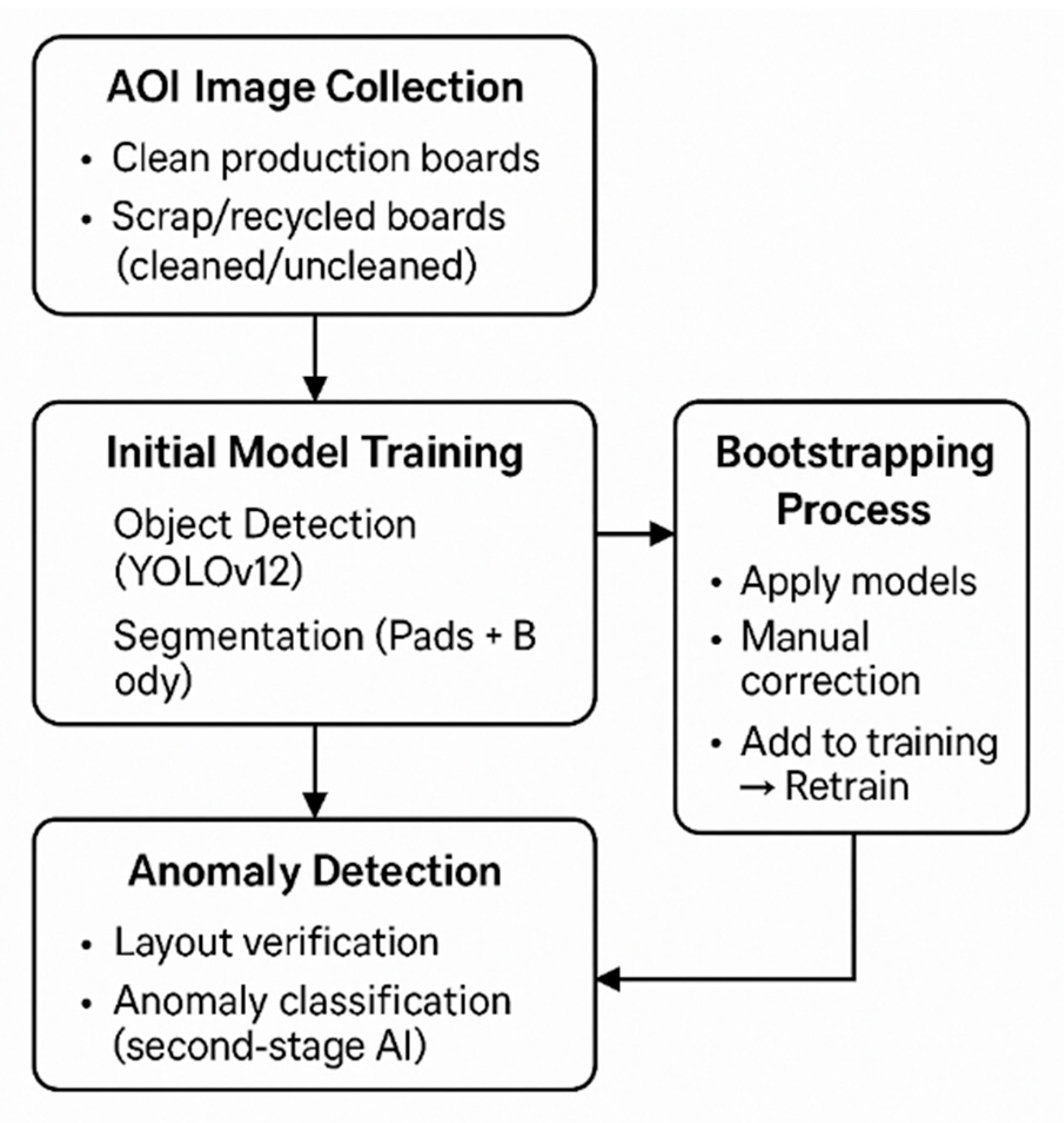
Figure 2.
Component detection on a pristine board. The top image shows a high-resolution AOI image processed by the object detection model, with red bounding boxes accurately localizing all visible components. The bottom image displays extracted metadata from the same image, illustrating how detection results serve as the basis for downstream anomaly analysis.
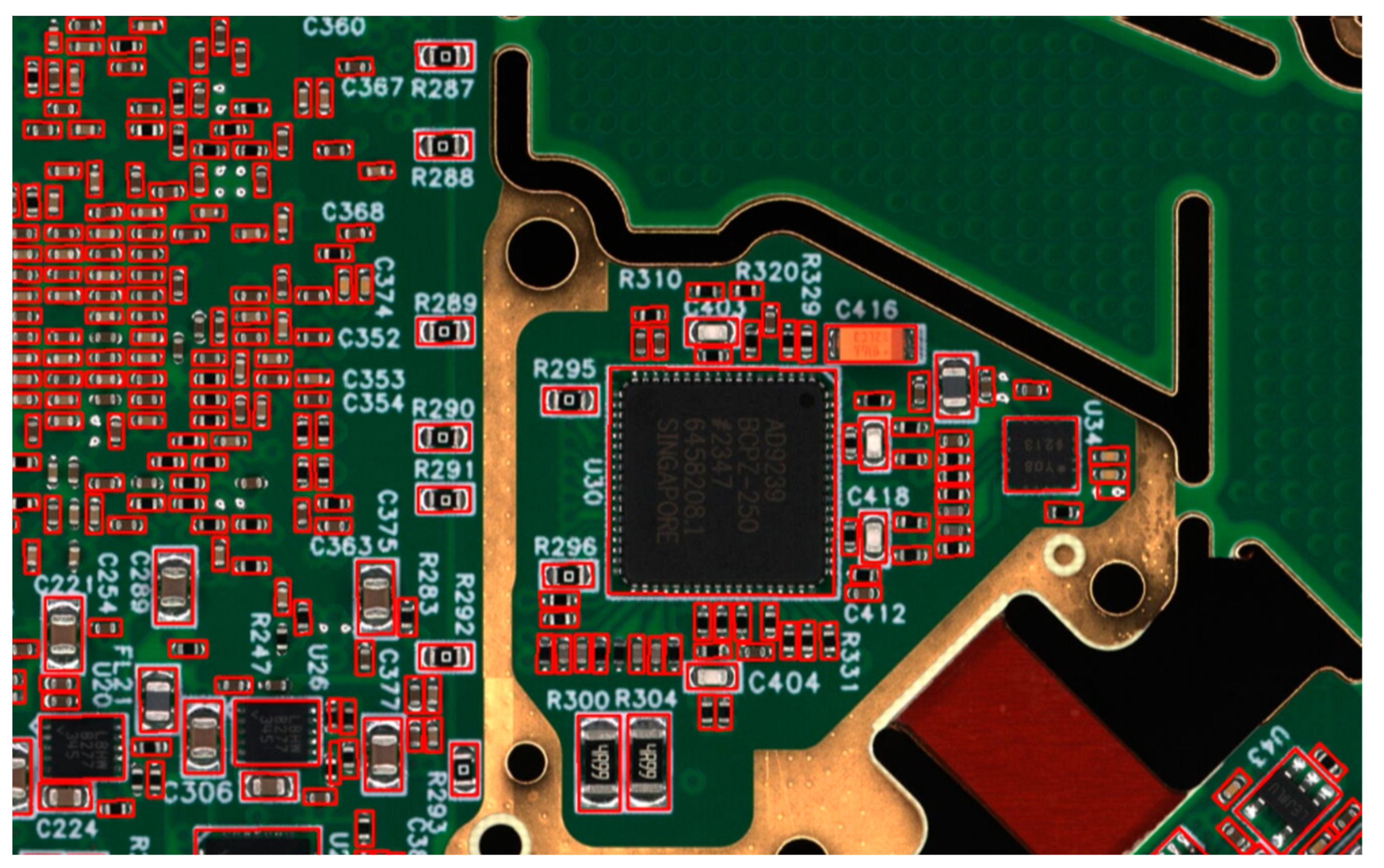
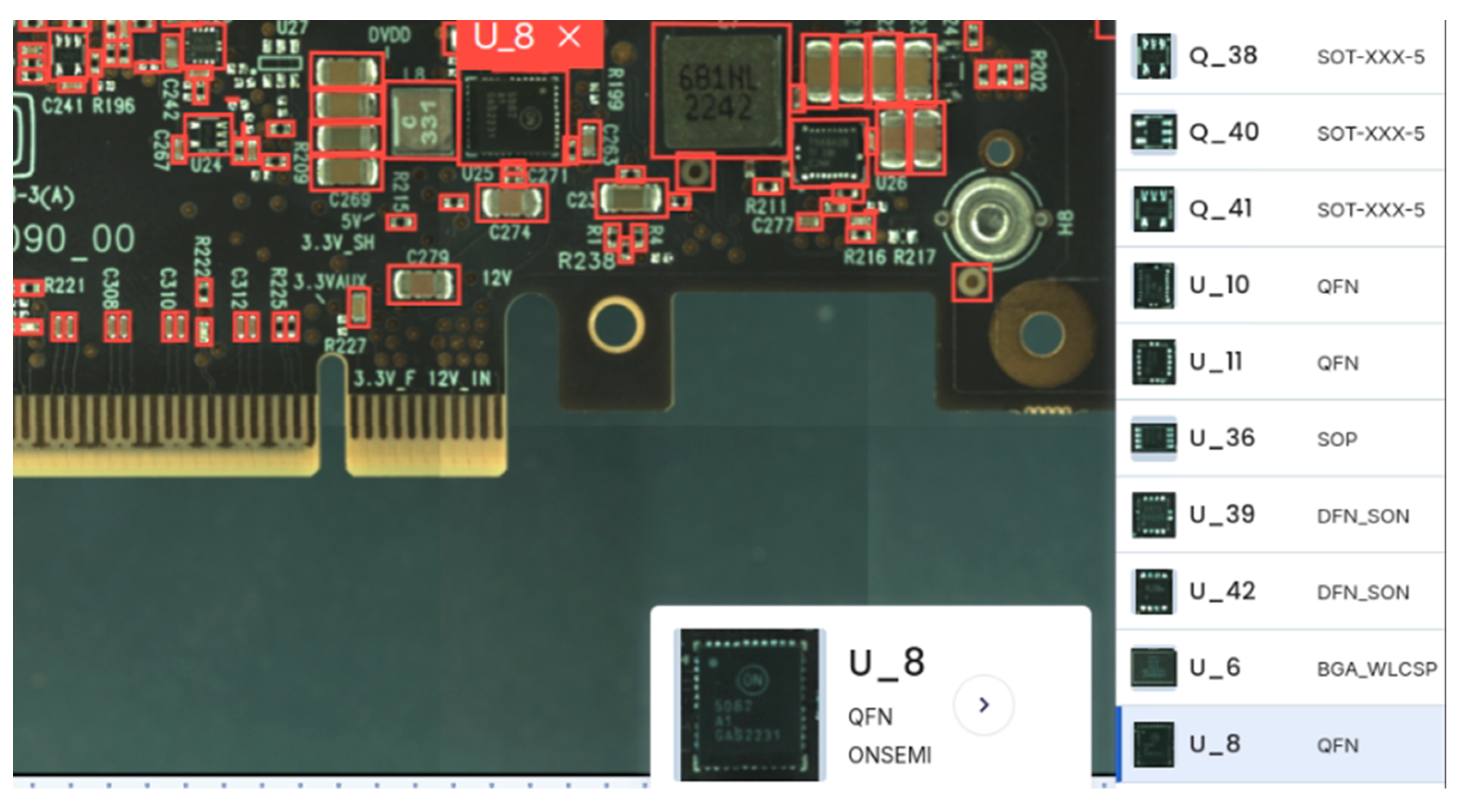
Figure 3.
Component-Level Segmentation Results. Output from the semantic segmentation model showing detailed masking of each component’s body (shown in blue) and the associated solder pad regions (highlighted in red). These masks enable fine-grained geometric comparisons with the golden reference.
Figure 3.
Component-Level Segmentation Results. Output from the semantic segmentation model showing detailed masking of each component’s body (shown in blue) and the associated solder pad regions (highlighted in red). These masks enable fine-grained geometric comparisons with the golden reference.
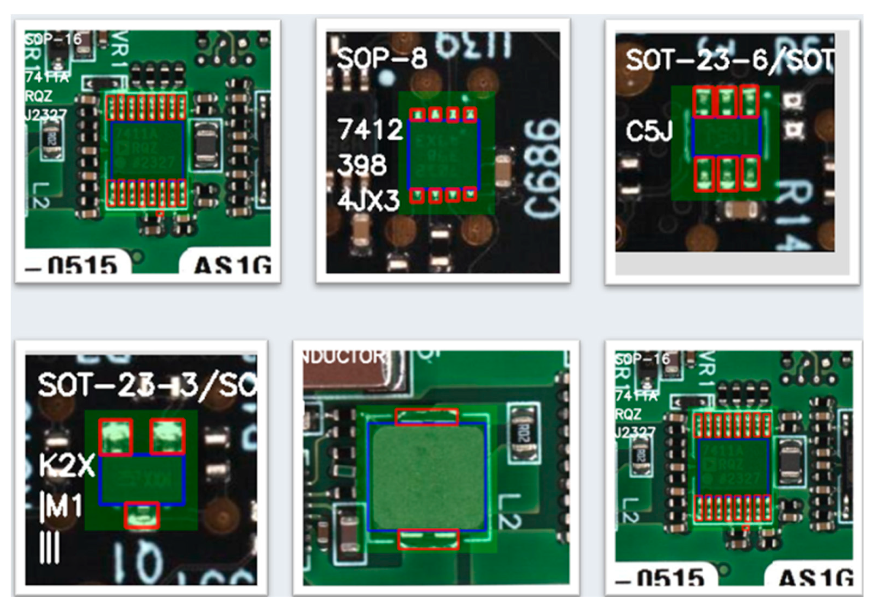
Figure 4.
Training Dynamics Across 360 Epochs. Loss convergence for object detection, including classification, regression, and localization components. Plots show steady improvement and alignment of validation and training losses, supporting the stability and generalization of the model. [X].
Figure 4.
Training Dynamics Across 360 Epochs. Loss convergence for object detection, including classification, regression, and localization components. Plots show steady improvement and alignment of validation and training losses, supporting the stability and generalization of the model. [X].
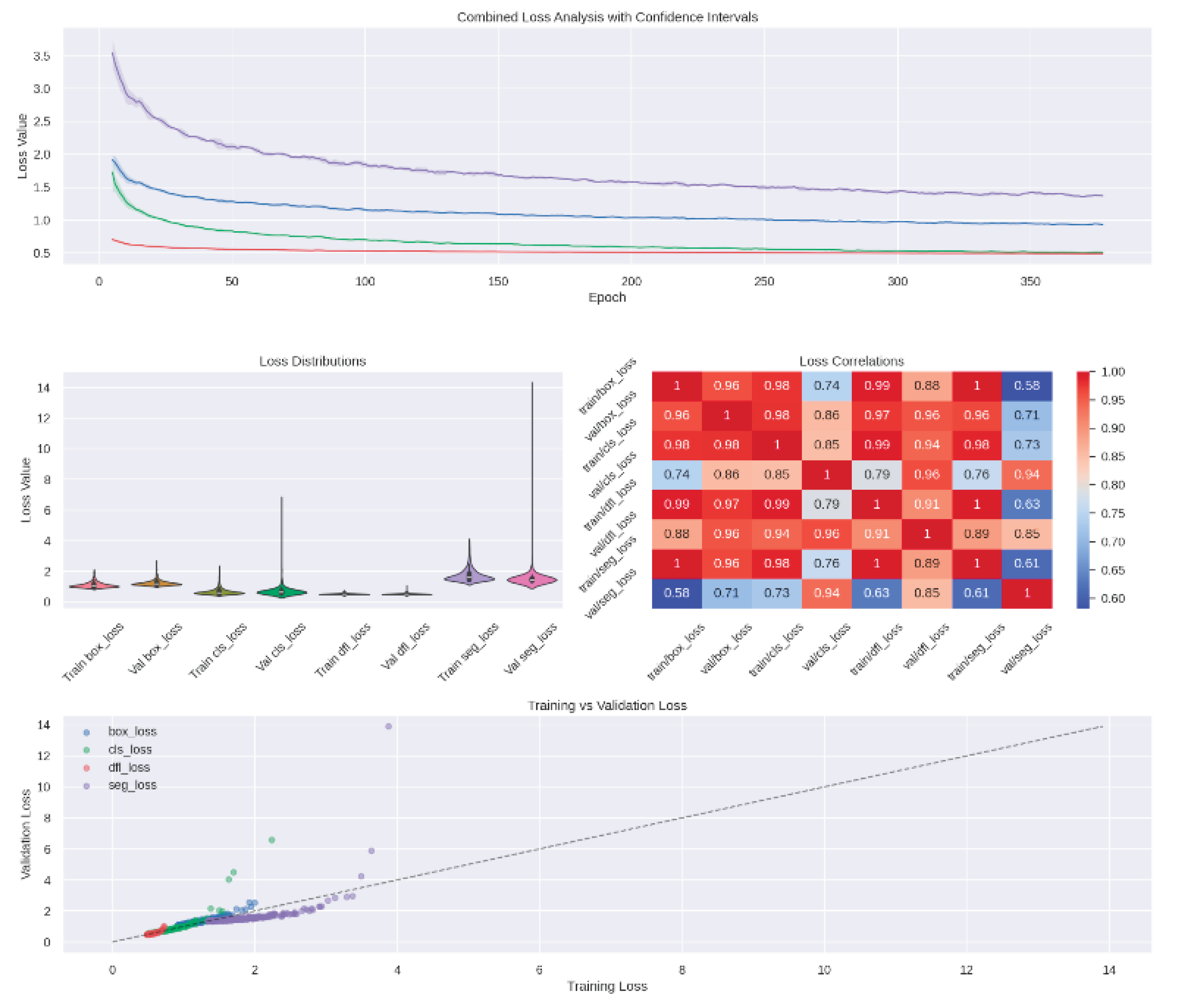
Figure 5.
Precision-Confidence Curve for Segmentation. Illustrates how segmentation performance varies with detection confidence. The model maintains an aggregate precision of 0.92, with consistent behavior across body and pad classes.
Figure 5.
Precision-Confidence Curve for Segmentation. Illustrates how segmentation performance varies with detection confidence. The model maintains an aggregate precision of 0.92, with consistent behavior across body and pad classes.
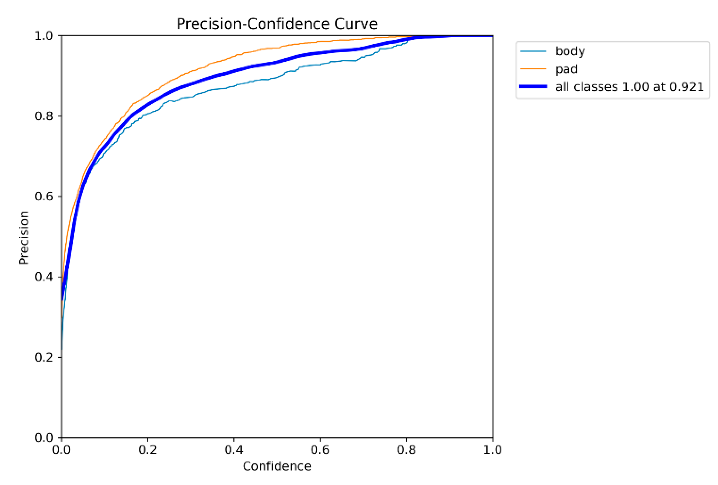
Figure 6.
Detection of layout-level anomalies in top-side inspection. The visual AI system identifies deviations on the PCB surface itself, such as unexpected features, irregularities, or marks, by comparing each board to a learned reference layout. Anomalies are highlighted in yellow, providing clear visual evidence for review, even when they occur outside expected component locations.
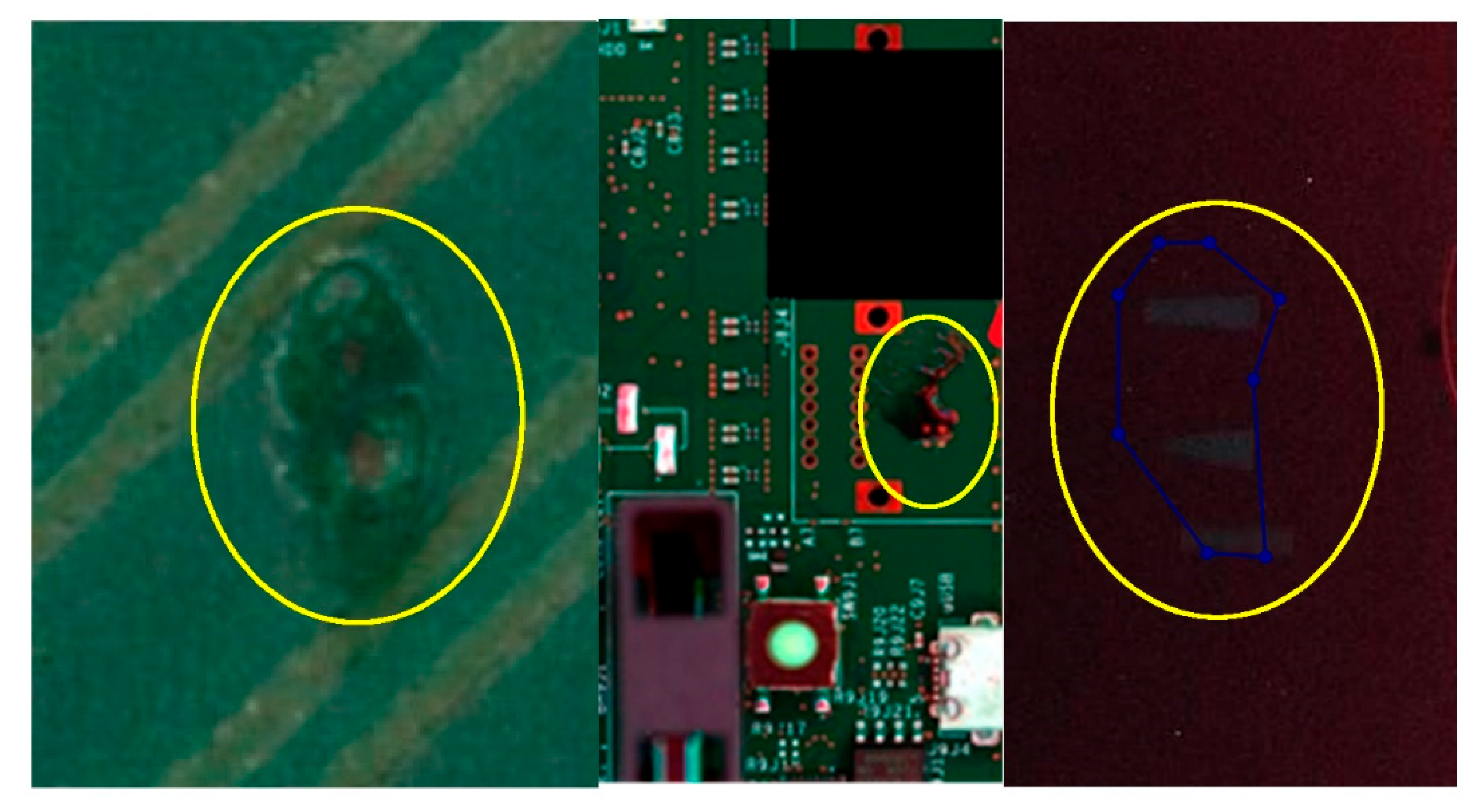
Figure 7.
Detection of unauthorized and misplaced components using top-side visual inspection. The top row shows examples of components that were unintentionally scattered across the PCB during placement, as well as a missing component footprint, highlighted in yellow. These anomalies fall outside standard AOI inspection zones and are detected by adaptive visual AI. The bottom row presents the system’s automated detection of a piggybacked component, an unauthorized part soldered on top of an existing IC (U_8). The algorithm identifies inconsistencies in geometry and position, flagging the tampering attempt based on deviations from learned visual patterns.
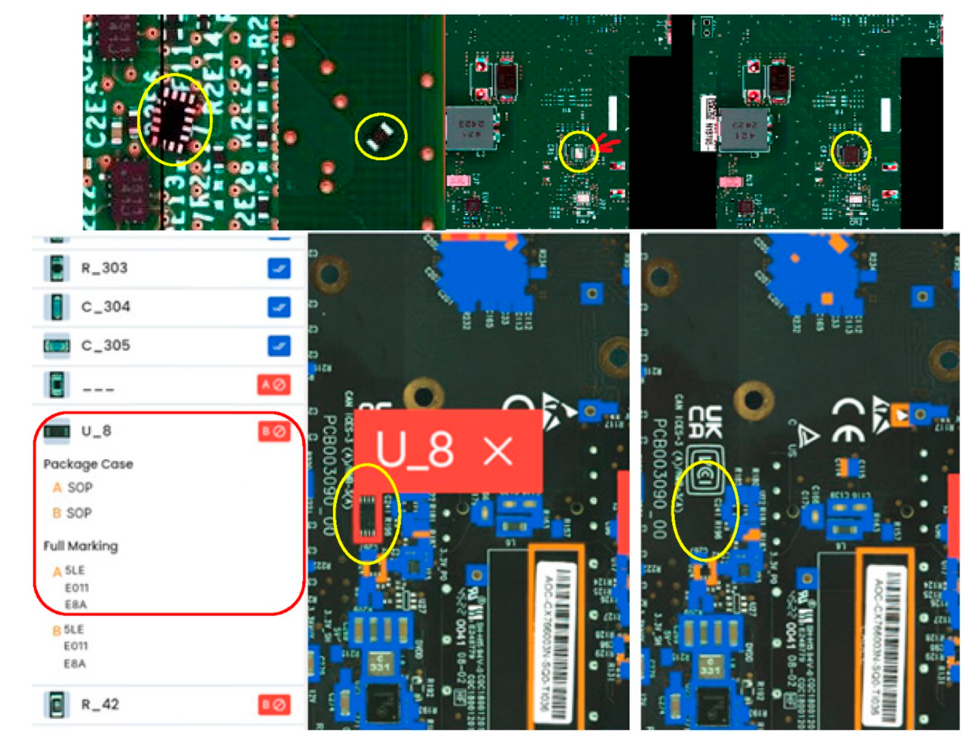
Figure 8.
Detection of unauthorized physical modifications on assembled PCBs. Left: A blue wire was manually added across component pins, representing a post-production rework or tampering attempt. The deviation was identified by the visual AI system due to its inconsistency with the expected layout. Right: A detached label was found adhered to the PCB surface, potentially obscuring markings or interfering with optical inspection. Both anomalies—circled in yellow and blue—fall outside predefined inspection regions and were flagged as unexpected by the AI-based detection framework.
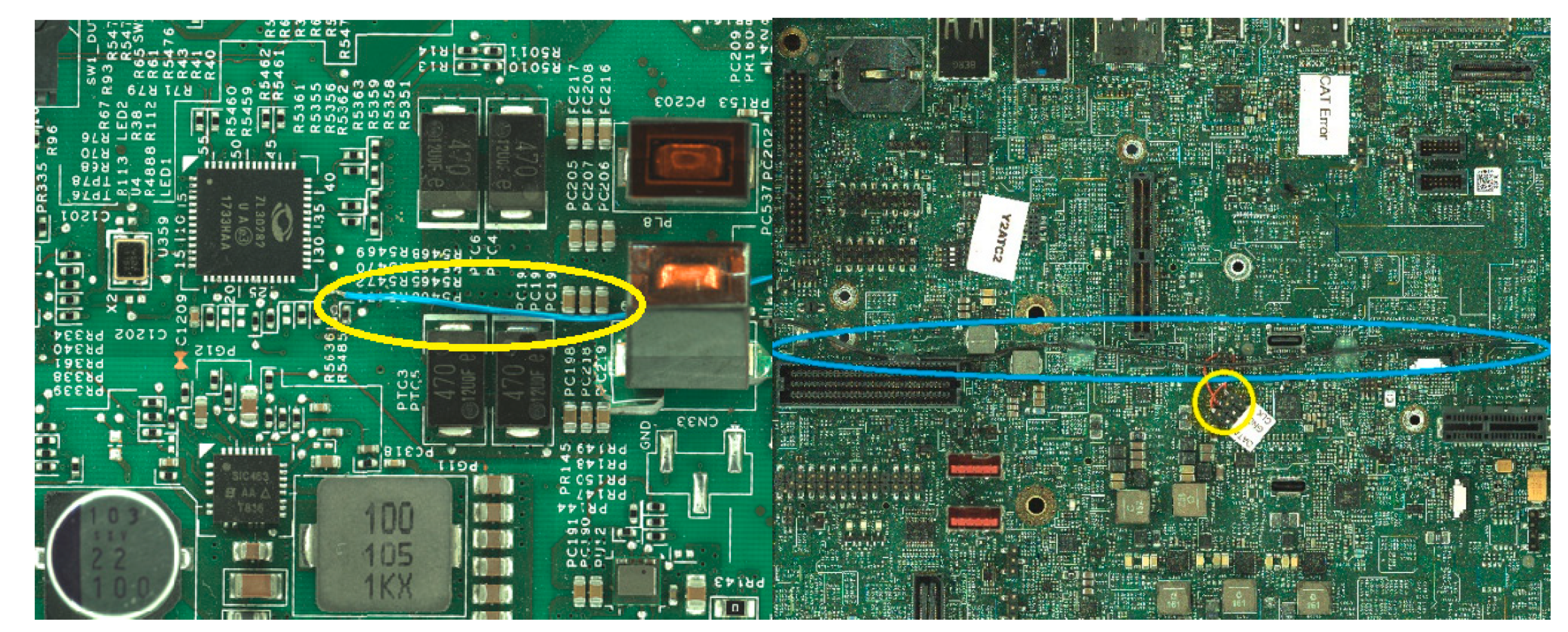
Figure 9.
Detection of unauthorized component substitution. Left: Golden reference visualization based on 50 production boards showing consistent package shape and markings for the approved crystal oscillator. Right: Test board with a substituted oscillator from a different manufacturer. Differences in surface finish, pad layout, and silkscreen alignment were flagged by the anomaly detection system.
Disclaimer/Publisher’s Note: The statements, opinions and data contained in all publications are solely those of the individual author(s) and contributor(s) and not of MDPI and/or the editor(s). MDPI and/or the editor(s) disclaim responsibility for any injury to people or property resulting from any ideas, methods, instructions or products referred to in the content. |
© 2025 by the authors. Licensee MDPI, Basel, Switzerland. This article is an open access article distributed under the terms and conditions of the Creative Commons Attribution (CC BY) license (http://creativecommons.org/licenses/by/4.0/).
Copyright: This open access article is published under a Creative Commons CC BY 4.0 license, which permit the free download, distribution, and reuse, provided that the author and preprint are cited in any reuse.


