
Submitted:
24 October 2025
Posted:
27 October 2025
You are already at the latest version
Abstract
Printed circuit board (PCB) defect detection is critical to manufacturing quality, yet tiny, low-contrast defects and limited annotations challenge conventional systems. This study develops an enhanced one-stage detector by modifying You Only Look Once (YOLO) version 5 (YOLOv5) with Efficient Channel Attention (ECA) for channel re-weighting, a lightweight Deformable Convolution (DCN) for geometric adaptability, a Bi-Directional Feature Pyramid Network (BiFPN) for multi-scale fusion, and Content-Aware ReAssembly of FEatures (CARAFE) for content-aware upsampling. A single-cycle semi-supervised training pipeline is further introduced: a detector trained on labeled images generates high-confidence pseudo-labels for unlabeled data, and the combined set is used for retraining without ratio heuristics. Evaluated on PKU-PCB under label-scarce regimes, the full architecture improves supervised mean Average Precision at an Intersection-over-Union threshold of 0.5 (mAP@0.5) from 0.870 (baseline) to 0.910, and reaches 0.943 mAP@0.5 with semi-supervision, with consistent class-wise gains and faster convergence. Ablation experiments validate the contribution of each module and identify robust pseudo-label thresholds, while comparisons with recent YOLO variants show favorable accuracy–efficiency trade-offs. These findings indicate that the proposed design delivers accurate, label-efficient PCB inspection suitable for Automated Optical Inspection (AOI) in production environments.
Keywords:
PCB defect detection
; semi-supervised object detection
; YOLO
1. Introduction
Printed circuit boards (PCBs) form the backbone of electronic systems by mechanically supporting and electrically connecting components. Even minor PCB surface defects – such as scratches, open circuits, or solder shorts – can cause malfunctions and degrade overall system performance [1]. Ensuring product quality and reliability therefore requires effective PCB defect detection. Traditionally, manufacturers have relied on manual visual inspection and automated optical inspection (AOI) for PCB quality control [2]. Manual inspection is labor-intensive and prone to inconsistency, while conventional machine-vision methods struggle with the complexity of PCB patterns and the diverse appearances of defects [2]. AOI techniques (e.g., template comparison or design-rule checking) can detect many defects but often require strict image alignment and controlled lighting; they also have difficulty generalizing to new defect types [3]. In practice, as new defect patterns continually emerge with changes in manufacturing processes, rule-based AOI systems must be frequently recalibrated to handle unseen anomalies [3]. These limitations, combined with the subjective and error-prone nature of human inspection, have driven a shift towards deep learning-based approaches for PCB defect detection [4].
Deep learning, especially convolutional neural networks (CNNs), can automatically learn discriminative visual features and has achieved superior accuracy in general image recognition tasks – in some cases even approaching or exceeding human-level performance [5]. By leveraging CNN models, PCB inspection systems become more adaptable to diverse or subtle defects without requiring explicit modeling of each defect type. In recent years, numerous studies have applied deep CNNs to PCB defect detection and reported significant improvements in detection accuracy over traditional methods [4]. For example, a 2021 study by Kim et al. developed a skip-connected convolutional autoencoder to identify PCB defects and achieved a detection rate up to 98% with false alarm rate below 2% on a challenging dataset [1]. This demonstrates the potential of deep learning to provide both high sensitivity and reliability in detecting tiny flaws on PCB surfaces, which is critical for preventing failures in downstream electronics.
Object detection models based on deep learning now dominate state-of-the-art PCB inspection research [6]. In particular, one-stage detectors such as the You Only Look Once (YOLO) family have gained popularity for industrial defect detection due to their real-time speed and high accuracy [7,8]. Unlike two-stage detectors (e.g., Faster R-CNN) that first generate region proposals and then classify them, one-stage YOLO models directly predict bounding boxes and classes in a single forward pass – making them highly efficient [6,8]. Early works demonstrated the promise of YOLO for PCB defect detection. For example, Adibhatla et al. applied a 24-layer YOLO-based CNN to PCB images and achieved over 98% defect detection accuracy, outperforming earlier vision algorithms [9]. Subsequent studies have confirmed YOLO’s advantages in this domain, showing that modern YOLO variants can even rival or surpass two-stage methods in both detection precision and speed [6,8]. The YOLO series has evolved rapidly—from v1 through v8 and, most recently, up to v11—with progressive architectural and training refinements (e.g., stronger backbones, decoupled/anchor-free heads, improved multi-scale fusion, advanced data augmentation, and Intersection-over-Union (IoU) aware losses) that collectively enhance accuracy–latency trade-offs across application domains [10] For instance, the latest YOLO models employ features like cross-stage partial networks, mosaic data augmentation, and CIoU/DIoU losses to better detect small objects and improve localization [11,12]. YOLOv5, in particular, has become a widely adopted baseline in PCB defect inspection, valued for its strong balance of accuracy and efficiency in finding tiny, low-contrast flaws in high-resolution PCB images [13,14]. Open-source implementations of YOLOv5 provide multiple model sizes (e.g., YOLOv5s, m, l, x) that can be chosen to trade off speed and accuracy, facilitating deployment in real-world production settings [13]. However, standard YOLO models still encounter difficulties with certain PCB inspection challenges, such as extremely small defect targets, complex background noise, and limited training data. This has motivated researchers to embed additional modules into the YOLO framework and to explore semi-supervised training strategies tailored to PCB defect detection.
One major challenge in PCB defect inspection is the very small size and subtle appearance of many defect types (e.g., pinhole voids, hairline copper breaks). These tiny defects may occupy only a few pixels and can be easily missed against intricate PCB background patterns [4]. To address this, recent works have integrated attention mechanisms into YOLO detectors to help the network focus on important features. In particular, channel attention modules such as the Squeeze-and-Excitation (SE) and Convolutional Block Attention Module (CBAM) have been added to emphasize defect-relevant feature channels and suppress irrelevant background information [15]. For example, Xu et al. reported that inserting a CBAM module into a YOLOv5-based model improved recognition of intricate, small PCB defects under complex backgrounds by enhancing the model’s attention to critical regions. A lightweight variant, Efficient Channel Attention (ECA), has proved effective in detection settings; by applying a short 1-D convolution to model local cross-channel dependencies—without the dimensionality reduction used in SE/CBAM—ECA enhances feature saliency with negligible computational overhead [16]. Kim et al. demonstrated that adding an ECA module into a YOLOv5 backbone boosted the detection of small objects in aerial images, as the channel attention helped highlight faint targets against cluttered backgrounds [16]. Similarly, an enhanced YOLOv5 model for surface inspection found that integrating ECA improved the identification of fine defects (especially tiny or low-contrast features) compared to using SE attention alone [17]. These findings underscore that incorporating efficient attention mechanisms enables YOLO models to better capture subtle defect cues that might otherwise be overlooked. A streamlined ECA module is embedded in the YOLOv5 backbone to adaptively accentuate faint PCB defect patterns, enabling clearer separation of true defect signals from background circuitry.
Another limitation of vanilla YOLO detectors lies in the fixed sampling grid of standard convolutions, which restricts the receptive field from conforming to irregular defect geometries on PCB. Deformable Convolutional Networks (DCN) alleviate this constraint by learning location-dependent offsets so that kernels adaptively sample informative positions, effectively “bending” to follow fine discontinuities, burrs, and spurious copper patterns. By aligning the sampling lattice with true object boundaries, deformable convolutions help prevent the mixing of faint defect signals with background textures and thereby preserve small-object detail during feature extraction [12]. Recent journal studies show that inserting a deformable layer into YOLO backbones or necks yields measurable gains on small-object benchmarks by retaining object cues and reducing background interference [18,19]. In the PCB context, improved YOLO variants that integrate DCN (or DCNv2) into high-resolution feature paths report enhanced localization of tiny, irregular defects and higher mean Average Precision, attributable to better spatial alignment around hairline breaks and micro-holes [20]. Beyond PCB imagery, complementary evidence from aerial and industrial surface datasets confirms that lightweight DCN blocks can be deployed with modest computational overhead to sharpen feature selectivity on thin, elongated structures—an effect particularly valuable for defect edges and gaps [19,21]. Following these insights, a DCN-lite layer is placed in the YOLOv5 neck to introduce spatial flexibility where fine spatial detail is most critical, aiming to increase sensitivity to minute or oddly shaped PCB anomalies while preserving throughput [20,22].
Effective multi-scale feature fusion is essential in PCB inspection, where target sizes span from large solder bridges to sub-pixel pinholes. While the original YOLOv5 neck adopts a Path Aggregation Network (PANet), recent work shows that bi-directional pyramid designs with learnable fusion weights strengthen small-object representations and improve robustness to scale variation. In particular, Bi-Directional Feature Pyramid Networks (BiFPN) iteratively propagate information top-down and bottom-up, balancing low-level spatial detail with high-level semantics and yielding consistent gains over PANet-style necks in one-stage detectors [23]. Journal studies report that replacing or augmenting PANet with BiFPN leads to higher precision and recall on small targets by avoiding attenuation of fine details during fusion [24]. In PCB-focused research, lightweight YOLO variants that integrate BiFPN in the neck achieve superior accuracy on micro-defects, indicating that normalized, weighted cross-scale aggregation is particularly beneficial for tiny, low-contrast structures [25]. Beyond PCB imagery, enhanced (augmented/weighted) BiFPN formulations further validate these trends in diverse vision tasks, demonstrating that learnable cross-scale weights can reduce information loss and emphasize discriminative cues at small scales [26]. Guided by this evidence, the proposed model adopts a BiFPN neck to more effectively blend high-resolution detail and contextual semantics before detection, improving sensitivity to both macro-level faults and minute solder splashes. [27,28].
In addition to stronger feature fusion, refining the upsampling operator in the neck materially benefits small-defect detection. Fixed schemes (e.g., nearest-neighbor) can blur fine edges and attenuate weak responses, causing misses on hairline cracks or pinholes [29]. A learnable alternative is Content-Aware ReAssembly of Features(CARAFE), which predicts position-specific reassembly kernels from local content and reconstructs high-resolution features with a larger effective receptive field [30]. Unlike fixed interpolation, CARAFE preserves boundary and texture cues during upscaling and has been shown to improve one-stage detectors on cluttered scenes with numerous tiny targets [31]. Recent journal studies report that inserting CARAFE into YOLO-style necks yields higher precision/recall on small objects while maintaining real-time feasibility due to the module’s lightweight design [32]. Further evidence from remote-sensing benchmarks indicates that CARAFE reduces information loss and better aligns multi-scale features compared with naïve interpolation, boosting mAP for dense small targets [33]. Guided by these results, the present YOLOv5-based architecture replaces nearest-neighbor upsampling with CARAFE at top-down pathways to retain minute PCB defect details during feature magnification and to strengthen the downstream detector’s sensitivity to thin, low-contrast flaws [34].
While architectural enhancements increase capacity, data scarcity and class imbalance remain practical bottlenecks in PCB defect inspection. In early production or when new defect modes emerge, only a handful of labeled samples may exist, making fully supervised training prone to overfitting and poor generalization. Semi-supervised object detection (SSOD) addresses this by exploiting large pools of unlabeled imagery together with few labels, commonly through pseudo-labeling and consistency regularization in teacher–student schemes [35,36]. This setting aligns well with PCB lines, where acquiring images at scale is easy but fine-grained annotation is costly; leveraging unlabeled frames expands the distribution of backgrounds, lighting, and rare defects seen during training [35,37]. Recent journal studies demonstrate that filtering uncurated unlabeled sets and enforcing consistency across augmentations markedly improves pseudo-label quality and downstream detection, boosting mAP in low-label regimes [35]. Practical SSOD variants also integrate adaptive thresholds or active selection to suppress noisy pseudo-boxes while retaining diverse positives, further stabilizing one-stage detectors [38,39]. Guided by these findings, a single-cycle self-training pipeline is adopted: a detector trained on labeled PCB images generates high-confidence pseudo-labels on unlabeled data; the labeled and pseudo-labeled samples are then mixed without ratio heuristics for retraining, improving recall of subtle anomalies while keeping computational overhead modest [36,40]. In effect, training on both labeled and pseudo-labeled data broadens coverage of rare, small, and low-contrast defects, reducing false negatives and improving robustness in deployment [36,40].
This study presents a task-aligned one-stage PCB defect detector by augmenting YOLOv5x with ECA, a lightweight DCN-lite, a BiFPN, and CARAFE upsampling. A single-cycle semi-supervised scheme (pseudo-labels with τ=0.60, IoU=0.50; random mixing with ground truth) expands effective training data. On PKU-PCB, supervised mAP@0.5 improves from 0.870 (baseline) to 0.910 with reduced complexity (63.9 M params; 175.5 GFLOPs vs. 86.2 M; 203.9). With semi-supervision, the baseline reaches 0.9115 mAP, while the proposed model attains 0.943 mAP, 94.4% precision, and 91.2% recall. Ablations confirm each module’s contribution and identify robust pseudo-label settings; comparisons with recent YOLO variants show favorable accuracy–efficiency trade-offs, yielding a label-efficient, deployment-ready AOI solution for tiny, low-contrast PCB defects.
2. Methods
Our approach comprises two main components: (1) a modified YOLOv5-based architecture with an enhanced backbone and neck (incorporating ECA, DCN-lite, BiFPN, and CARAFE modules), and (2) a one-stage semi-supervised training pipeline that leverages unlabeled data via pseudo-labeling. Each component is detailed below.
2.1. Network Architecture: YOLOv5x_ECA_DCN_BiFPN_CARAFE
An overview of the modified YOLOv5x architecture is shown in Figure 1 above. The network is built on a YOLOv5x backbone with four key module enhancements aimed at improving feature extraction and detection of small defects:
ECA (Efficient Channel Attention): Inserted into C3 backbone blocks to adaptively re-weight feature channels (highlighted in green in the diagram).
DCN-lite: A lightweight deformable convolution applied on the high-resolution P3 feature branch (stride 8) to introduce spatial sampling flexibility for small defects.
BiFPN with WA_SC: A bidirectional feature pyramid neck employing Weighted Add fusion followed by a Separable Convolution. Each fusion node learns non-negative weights to combine inputs (WeightedAdd), then uses a depthwise separable convolution for refinement.
CARAFE upsampling: A content-aware upsampling operator used in all top-down pathways, replacing standard interpolation to better preserve fine details..
2.1.1. Notation and Topology
Let the input image be (default S=640). The backbone outputs feature maps at strides (8, 16, 32). Lateral convolutions align channels before fusion. The neck performs a top-down pass (P5→P4→P3) using CARAFE upsampling and a bottom-up pass (P3→P4→P5) using strided depthwise separable convolutions. Each fusion node applies WeightedAdd to its inputs, followed by a depthwise separable refinement. The detector head predicts at strides 8, 16, and 32.
2.1.2. ECA inside C3
For a feature tensor ,
The kernel size kkk is a small odd number determined by the channel count via a mapping . ECA thus re-weights channels without dimensionality reduction, preserving efficiency.
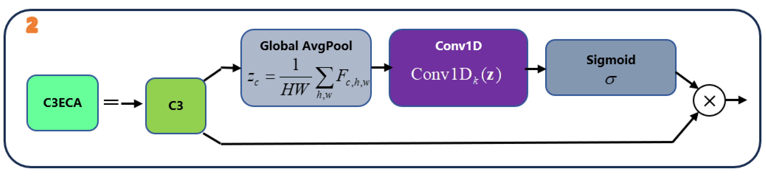
Figure 2.
Illustration of the ECA mechanism placed inside the C3 block. Global average pooling yields the channel descriptor ; a lightweight 1D convolution of size k followed by a sigmoid generates attention weights , which re-weight the original feature map. .
Figure 2.
Illustration of the ECA mechanism placed inside the C3 block. Global average pooling yields the channel descriptor ; a lightweight 1D convolution of size k followed by a sigmoid generates attention weights , which re-weight the original feature map. .
2.1.3. CARAFE Content-Aware Upsampling
Given a low-resolution feature map and upsampling factor , CARAFE first encodes local contentt:
and predicts spatially varying reassembly kernels
Let denote the unfolded patches of .For each low-res location and subpixel offset (corresponding to offset (, )), the high-resolution output is reconstructed as
In the top-down path (P5→P4, P4→P3), CARAFE replaces fixed interpolations, preserving fine edges and small patterns with minimal overhead.
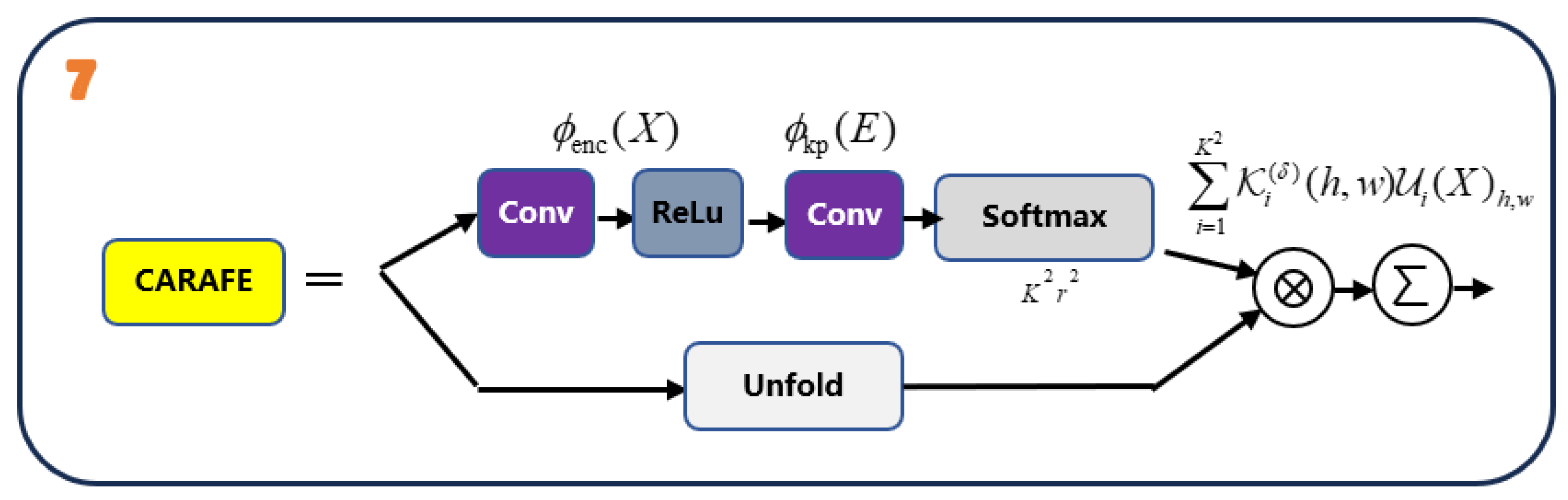
Figure 3.
The CARAFE mechanism: content encoding and kernel prediction generate position-adaptive reassembly kernels; unfolded neighborhood features are then reassembled to produce the upsampled output.
Figure 3.
The CARAFE mechanism: content encoding and kernel prediction generate position-adaptive reassembly kernels; unfolded neighborhood features are then reassembled to produce the upsampled output.
2.1.4. BiFPN-Style Fusion with WeightedAdd and Separable Convolution
For inputs entering a fusion node, learnable non-negative weights are normalized as
A depthwise-separable convolution (DW 3×3 + PW 1×1) refines Y. Top-down nodes fuse ;bottom-up nodes fuse . This learnable, normalized fusion balances semantic context and spatial detail.
Figure 4.
Schematic of the BiFPN bidirectional feature fusion. Each fusion node performs WeightedAdd with normalized weights and a separable refinement.
Figure 4.
Schematic of the BiFPN bidirectional feature fusion. Each fusion node performs WeightedAdd with normalized weights and a separable refinement.
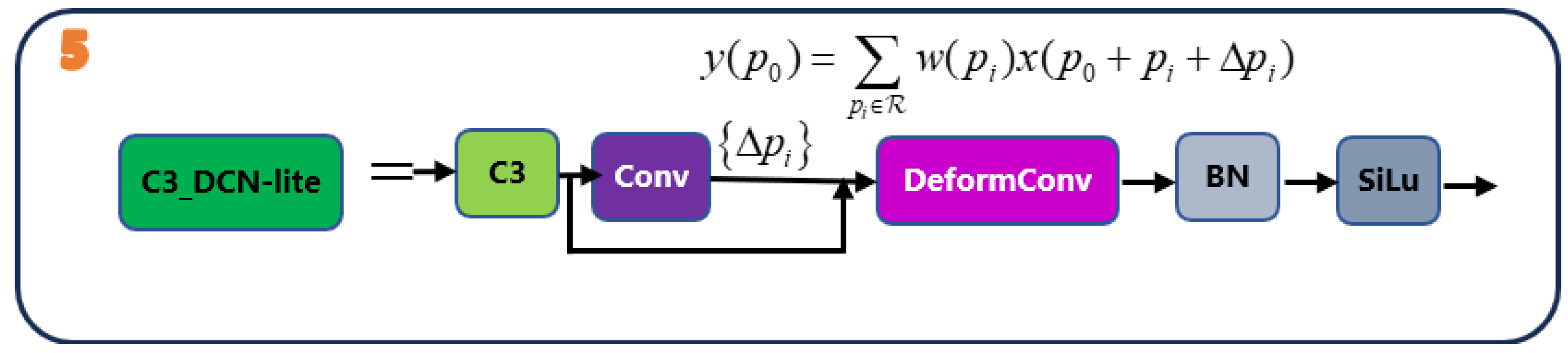
2.1.5. DCN-Lite on the High-Resolution Path (P3)
A single DCN-lite is applied to the P3 branch (stride-8) to introduce localized geometric flexibility with minimal latency overhead.For input feature map xxx and learned offsets on the sampling grid
where bilinear interpolation is used for non-integer coordinates. Concentrating the deformable operation at the finest resolution (P3) enhances sensitivity to small and irregular defects while keeping the model lightweight.
Figure 5.
Incorporating a DCN-lite module on the P3 feature map. Offsets are predicted by a lightweight conv; samples are gathered via bilinear interpolation, followed by BN and SiLU.
Figure 5.
Incorporating a DCN-lite module on the P3 feature map. Offsets are predicted by a lightweight conv; samples are gathered via bilinear interpolation, followed by BN and SiLU.
2.2. One-Stage Semi-Supervised Training
The training scheme exploits unlabeled images via a single-cycle pseudo-label self-training pipeline: supervised pre-training → pseudo-label generation → retraining on a mixed pool. No EMA teacher, test-time augmentation (TTA), or labeled/unlabeled sampling-ratio heuristics are used.
2.2.1. Notation
Let the labeled and unlabeled sets be
For an image, the detector outputs boxes ,class posteriors , and objectness ,The detection confidence is
2.2.2. Stage A — Supervised Pre-Training
Model parameters are optimized on with the EDBC-YOLO detection loss
The loss is a weighted sum of box, objectness, and classification terms over the three detection layers , ,
The YOLOv5 default gains are set as (on positives);
is BCE objectness with IoU-based soft targets for positives and 0 for negatives; is BCE classification (with optional small label smoothing). Layer-balance coefficients also follow the YOLOv5 defaults.
2.2.3. Stage B — Pseudo-Label Generation
Using , inference is run over all .After NMS, predictions with are retained as pseudo-annotations:
The threshold τ is fixed throughout.
2.2.4. Stage C — Retraining on the Mixed Pool (Uniform Sampling)
The mixed training set is
Mini-batches are sampled uniformly at random from without source-ratio control. The objective is
treating pseudo-labels and ground-truth labels identically (i.e., z may be a labeled or pseudo-labeled sample).
2.2.5. Flowchart and Implementation Remarks
Figure 6 visualizes the single-cycle procedure. Stage A trains on labeled data to obtain Stage B generates pseudo-labels on by confidence thresholding Stage C retrains on with uniform sampling and the same detection loss for both label sources.
Implementation details.
Sampling. Mini-batches are drawn uniformly at random from the mixed set ; no labeled/unlabeled ratio is enforced.
Confidence thresholding & NMS. A single, class-agnostic confidence threshold τ is used for pseudo-label generation (Stage B). The NMS configuration (e.g., IoU threshold) matches that used in validation for consistency.
Loss & assignment. The detection loss and anchor/assignment strategy follow the standard YOLOv5 implementation. Accepted pseudo-labels are treated as hard targets in Stage C, identical to ground-truth annotations.
2.3. Summary of Design Choices
Channel re-weighting: ECA inside C3 improves feature selectivity with negligible overhead (see Sec. 2.1.2).
Content-aware upsampling: CARAFE preserves fine structures while injecting context into high-res maps (Sec. 2.1.3).
Cross-scale fusion: BiFPN-style WeightedAdd provides normalized, non-negative fusion that balances semantics and detail (Sec. 2.1.4).
Geometric flexibility: A single P3 DCN-lite targets the finest scale, improving small-defect recall at low latency (Sec. 2.1.5).
Semi-supervision: One-cycle pseudo-labeling with uniform sampling yields measurable gains without teacher/TTA heuristics (Sec. 2.2).
3. Results
3.1. Data and Training Setup
Experiments are conducted on the PKU-PCB [41] dataset comprising six defect categories (open circuit, short circuit, mouse bite, spur, spurious copper, and pin-hole). To reflect realistic production constraints—few labeled images and many unlabeled images—the training data are split into a small labeled subset and a larger unlabeled pool, with independent validation and test sets held out.
The default semi-supervised configuration—which matches the dataset-split schematic is as table show:
All subsets are disjoint (no image overlap). Unlabeled images contribute to training only via pseudo-labels; the test set remains completely unseen until the final evaluation. The validation (600) and test (2134) splits remain fixed and non-overlapping across all experiments. This design enables controlled comparisons across label-scarce regimes while preserving a consistent, independent benchmark for model selection and final reporting.
Training Details. All experiments were conducted on a workstation equipped with a NVIDIA RTX 4090 (24 GB) GPU, an Intel® Xeon® Gold 6258R CPU, and 128 GB RAM. The software environment comprised Python 3.10 and PyTorch 2.1, running the official YOLOv5 codebase. Models were trained with a batch size of 16 using SGD (momentum 0.937, weight decay 5×10⁻⁴). The initial learning rate was 0.01 and followed a cosine decay schedule over the course of training. Each phase was run for up to 200 epochs, with early stopping triggered by a plateau in validation mAP to mitigate overfitting. Standard YOLOv5 data augmentations were enabled—random image scaling, horizontal flipping, color jitter, and Mosaic composition—to increase appearance diversity and improve generalization under limited labels. During inference, the confidence threshold was 0.25 (YOLOv5 default). For pseudo-label generation in the semi-supervised stage, a stricter threshold τ = 0.60 was applied to retain only high-confidence detections for retraining.
3.2. Evaluation Metrics
Detection quality is reported with precision (P), recall (R), average precision (AP), and the mean AP at IoU = 0.5 (mAP@0.5). Model size (Params) and computation (GFLOPs) are provided for complexity.
IoU. A prediction matches a ground-truth box if
Precision and Recall. With true positives (TP), false positives (FP), and false negatives FN,
High P indicates few false alarms; high R indicates few missed defects.
AP. For each class c, detections are sorted by confidence to form a precision–recall curve . The class AP is the area under this curve:
(implemented as the discrete, interpolated sum over recall breakpoints).
mAP@0.5. The primary metric averages AP across all C defect classes at the fixed IoU threshold 0.5:
Class-wise reporting. For each class, P, R, and are computed in a one-vs-all manner to reveal class difficulty; mAP summarize overall performance.
Complexity. Params is the total number of learnable weights. GFLOPs denotes the number of giga floating-point operations per image at test time, estimating computational cost.
3.3. Results and Analysis
3.3.1. Overall Performance and Module Ablation (Supervised)
The baseline YOLOv5x model is first evaluated against progressively enhanced variants under fully supervised training (using the available labeled training set) to quantify the impact of each architectural module. Table 1 summarizes the results. The baseline YOLOv5x achieves 87.0% mAP@0.5 on the PCB test set, with precision 91.9% and recall 83.5%. This high baseline underscores YOLOv5x’s strong starting point for PCB defect detection. Adding the Efficient Channel Attention block (+ECA) to YOLOv5x yields a slight mAP improvement to 88.0%, indicating better channel-wise feature focus on subtle defects. Incorporating a lightweight deformable convolution layer (+ECA+DCN) further raises mAP to 88.9% and improves recall (83.5% → 84.8%), confirming that spatially adaptive convolution helps detect a few more irregularly shaped defects. Replacing the standard upsampling with the CARAFE operator (+ECA+DCN+CARAFE) gives another modest boost (mAP 89.3%, recall 86.3%), suggesting better preservation of fine-grained features for small defect regions. The largest gain comes from introducing the BiFPN neck (+ECA+DCN+CARAFE+BiFPN), which produces our Full model. The Full model reaches 91.0% mAP@0.5 with precision 93.5%. The BiFPN’s stronger multi-scale feature fusion substantially improves detection of tiny, low-contrast defects, reflected in the higher overall accuracy. Notably, the Full model attains the highest mAP and also the highest precision among all variants, indicating that it not only finds more defects but also triggers fewer false alarms.
In addition to accuracy, our proposed modifications improve efficiency. Despite integrating several new modules, the Full model is actually lighter than the baseline YOLOv5x (parameters reduced from 86.2 M to 63.9 M) and requires fewer operations per inference (175 GFLOPs vs. 203.9 GFLOPs). This reduction is due to replacing some heavy layers with streamlined ones (e.g., using SPPF-lite and separable convolutions) and the BiFPN’s optimized topology. In summary, each architectural module contributed incremental gains, and together they delivered an overall +4.0 mAP point improvement (87.0 → 91.0) over the baseline (Table 2). The Full Arch model (YOLOv5x_ECA_DCN_CARAFE_BiFPN) achieves state-of-the-art performance on this task under full supervision.
Table 2 also includes YOLOv8 [42] and three recent improved YOLO-based detectors from the literature (YOLOv9–YOLOv11) [43-45]. The official YOLOv8 (with a model size of ~68 M) reached 87.4% mAP on our PCB test, slightly above the YOLOv5x baseline. YOLOv9 and YOLOv11 (from published methods) achieved around 88.8–88.9% mAP, indicating incremental improvements over YOLOv5 but still falling short of our Full model. Notably, our Full model outperforms all of these, with 91.0% mAP@0.5, establishing a new state-of-the-art for PCB defect detection under the same training conditions. It is worth mentioning that the Full model’s accuracy advantage comes without excessive model complexity – for instance, YOLOv9/YOLOv11 have slightly fewer parameters (≈58 M) but still lower accuracy (∼88.8% mAP), while YOLOv8 is both larger and less accurate than our model. This highlights that our combination of ECA, DCN-lite, CARAFE, and BiFPN is particularly effective for the unique challenges of PCB inspection (very small defects and complex backgrounds), yielding superior accuracy without undue model bloat. In other words, the targeted design of our modules provides a bigger payoff on this specialized task than generic YOLO improvements.
3.3.2. Training Convergence Across Architectures
Training curves of mAP@0.5 versus epoch number for the five model variants are plotted in Figure 7. All models exhibit a rapid initial rise in accuracy over the first ~20–30 epochs, followed by a more gradual improvement up to ~120 epochs, and then a plateau as training converges. Importantly, at any given epoch the curve for a model with an extra module lies at or above the curve for the less advanced model, indicating strictly monotonic improvements from each architectural addition. The Baseline (YOLOv5x) saturates at the lowest mAP (~0.87), whereas adding ECA shifts the entire learning trajectory upward (even the early epochs start higher), reflecting better channel-attention focus on relevant features. Adding the DCN-lite accelerates mid-phase learning (steeper gain around 40–80 epochs) consistent with improved geometric flexibility. Replacing nearest-neighbor upsampling with CARAFE yields a modest but steady uplift and also smooths out minor fluctuations near convergence, suggesting more stable feature interpolation. Finally, the Full model (with BiFPN) not only reaches the highest final mAP (~0.91) but also converges faster than the others, with its curve separating from the pack early on. By epoch ~100, the Full model virtually attains its peak, whereas the Baseline still creeps up slowly. This indicates that the enhanced architecture learns more efficiently from limited data. Throughout training, the performance ranking remains consistent – Baseline < +ECA < +ECA+DCN < +ECA+DCN+CARAFE < Full – mirroring the final test-set results in Table 1. In practical terms, these dynamics mean that our Full model can achieve a given accuracy in fewer epochs, which is advantageous for faster experimentation and deployment.
3.3.3. Semi-Supervised Learning Results
Semi-Supervised vs. Supervised Training: Leveraging unlabeled data via semi-supervised learning (SSL) led to substantial performance gains. Table 3 compares the final detector’s results after semi-supervised training with the corresponding supervised-only results. Using the baseline YOLOv5x architecture, adding the SSL procedure (with 100 labeled images and 1000 unlabeled images in training) improved mAP from 87.0% to 91.15%, and increased recall from 83.5% to 87.4%. This indicates that pseudo-labeling the additional 1000 PCB images effectively enhanced the model’s ability to catch more defects (higher recall) without sacrificing precision (which also rose to 93.6%). For the full proposed architecture, semi-supervised training provided an even larger boost: the mAP climbed from 91.0% to 94.3%, with precision 94.4% and recall 91.2%. In other words, our model trained with unlabeled data achieves 94.3% detection mAP@0.5 – an absolute improvement of ~3.3 points over the supervised version and ~7.3 points over the supervised baseline. These results validate that the one-stage SSL strategy markedly improves defect detection performance, especially by reducing false negatives (since recall gains are most pronounced). The extra unlabeled examples expose the detector to a wider diversity of PCB appearances and defect instances, mitigating overfitting to the small labeled set.
An additional advantage of our approach is its label efficiency. With the semi-supervised pipeline, very high accuracy can be achieved even with only a small fraction of the data labeled. For instance, our Full+SSL model can exceed 90% mAP with only on the order of dozens of labeled images, by learning from hundreds of unlabeled samples via pseudo-labeling (a scenario that would yield far lower accuracy if trained supervised-only). This data-efficient learning is extremely valuable in real production settings where labeling is expensive (see Practical Implications below). In summary, leveraging unlabeled data via SSL markedly improves detection – especially by increasing recall – and our results show this holds across different label budgets.
3.3.4. Class-Wise Detection Performance
To understand performance per defect type, Table 4 breaks down the precision, recall, and AP@0.5 for each of the six PCB defect classes, comparing the baseline, the Full model, and the Full model with SSL. The Full architecture provides consistent improvements over the baseline for all defect categories, and incorporating unlabeled data (Full+SSL) further boosts performance, most prominently in recall. For example, for the “short circuit” defect (which the baseline found relatively challenging), the baseline model obtains AP=80.7% with recall 77.6%. The Full Arch model improves this to AP=87.6% and recall 82.7%, and with SSL it reaches AP=89.8% and recall 88.8%, substantially reducing missed short-circuit defects. Similar trends are observed in other classes: for “spur” defects, AP rises from 83.0% → 87.4% → 92.4% moving from baseline to Full to Full+SSL, driven by recall improving from 76.4% → 77.6% → 86.5%. Even for classes where baseline precision was already very high (e.g., “pin-hole”, P≈98%), the Full model and SSL manage to increase recall (baseline 92.4% → Full 95.8% → Full+SSL 97.9%) and achieve the highest AP (98.5%). These results indicate that our proposed modules and semi-supervised training generalize across defect types – every category sees an increase in detection quality, and the greatest gains come in catching difficult instances (recall). The Full+SSL model does especially well on defects that are tiny or low-contrast (e.g., spurious copper, pin-holes), where it dramatically reduces false negatives compared to the baseline. Overall, the class-wise analysis confirms that the improved detector is robust across all defect categories, offering both higher sensitivity and precision than the original YOLOv5x.
3.3.5. Qualitative Results
Figure 8 presents side-by-side qualitative comparisons on six test boards, with red boxes for the baseline YOLOv5x, blue for the Full+SSL detector, and green for ground truth. The top row (a–c) targets spur (a) and spurious copper defects (b–c). In all three cases, the baseline produces incorrect detections—either false alarms or mislocalized boxes—whereas the Full+SSL predictions align with the annotations, removing the false positives and tightening localization around the actual defect regions. The bottom row (d–f) examines open circuit (d) and spurious copper defects (e–f). Here the baseline misses the defects entirely (no correct red boxes at the GT sites), while the Full+SSL model successfully recovers all targets with boxes that closely match the ground truth. Overall, the top-row examples illustrate the precision benefit (fewer false positives), and the bottom-row examples highlight the recall improvement (fewer misses). The visual evidence corroborates the quantitative results reported in Table 3, demonstrating that the proposed architecture plus semi-supervised training yields both more reliable detections and tighter localization for tiny, low-contrast PCB defects.
4. Conclusions
A PCB defect detection approach is presented that enhances the one-stage YOLOv5 detector with multiple architectural improvements and a semi-supervised training paradigm. The proposed model, termed PCB-SSD (Single-Stage Detector), integrates ECA, a DCN-lite deformable convolution, a BiFPN multi-scale feature fusion neck, and CARAFE upsampling into the YOLOv5x framework, and is trained with an iterative self-training scheme to leverage unlabeled data. Comprehensive experiments on a challenging PCB defect dataset show that each modification contributes to improved performance. The final Full+SSL model achieved 94.3% mAP@0.5 on the test set with 94.4% precision and 91.2% recall, significantly outperforming the baseline YOLOv5x (87.0% mAP, 91.9% precision, 83.5% recall). This result not only surpasses the baseline by a wide margin but also exceeds the accuracy of several state-of-the-art YOLO variants in the literature, especially in detecting the tiny, low-contrast defects that challenge conventional methods. Key findings and contributions of our study include: (1) The addition of lightweight attention and feature-fusion modules (ECA, BiFPN) markedly improved the model’s ability to localize small defects by focusing on important channels and combining information across scales; (2) The DCN-lite added valuable flexibility to model irregular defect shapes, and CARAFE preserved fine detail, together leading to more precise defect localization; (3) The semi-supervised training strategy proved highly effective – by learning from a large pool of unlabeled PCB images, the detector’s recall of defects increased substantially (and precision also improved), enabling reliable detection even with very limited labeled data. For instance, our model can exceed 90% mAP with only a few dozen labeled images by leveraging hundreds of unlabeled samples via pseudo-labeling. These contributions represent a practical advancement for PCB inspection: a single-stage model that is both more accurate and more data-efficient than previous solutions.
In terms of practical implications, the improved defect detector offers tangible benefits for manufacturing quality control. Its high accuracy and low false-alarm rate mean it can serve as a dependable AOI system on the production line, reducing the burden on human inspectors and catching defects that might otherwise be overlooked. Moreover, the ability to train robustly with very few labeled examples but many unlabeled ones is particularly useful in real production environments – it alleviates the typical data bottleneck, since capturing a large volume of PCB images is relatively easy, but manually labeling them is time-consuming and costly. Using our approach, manufacturers could deploy an initial model with minimal annotation effort and continuously improve it by incorporating streams of new unlabeled images (with automatic self-labeling) from ongoing production. This facilitates an adaptable defect detection system that keeps learning as new boards or new defect types emerge, without requiring exhaustive labeling for each change. Additionally, the model’s one-stage design is computationally efficient (with moderate model size and FLOPs), making it feasible to run in real-time on modern industrial GPUs or even edge devices on the factory floor for in-situ inspection.
In conclusion, this work demonstrates a successful fusion of modern object detection enhancements and semi-supervised learning for PCB defect inspection. The proposed Full+SSL model significantly outperforms the prior state-of-the-art on the PCB dataset, especially in detecting challenging tiny defects, while using far fewer labeled examples. These results advance the development of smarter, more reliable automated PCB inspection systems. The methodology is general and could be extended to other electronic inspection or manufacturing quality-control tasks where labeling data is difficult – combining powerful one-stage detectors with unlabeled data is a promising direction for achieving high accuracy at low annotation cost. Future research may explore applying this approach to different defect datasets or integrating more advanced pseudo-label refinement strategies (e.g., adaptive thresholds or uncertainty estimation) to further improve performance. The findings are expected to stimulate further advances in data-efficient deep learning for industrial inspection, moving toward AI systems that continuously learn and improve with minimal human intervention.
Author Contributions
Conceptualization, Zhenxia Wang (Z.W.), Nurulazlina Ramli (N.R.) and Tzer Hwai Gilbert Thio (T.H.G.T.); methodology, Z.W.; software, Z.W.; validation, Z.W.; formal analysis, Z.W.; investigation, Z.W.; resources, N.R. and T.H.G.T.; data curation, Z.W.; writing—original draft preparation, Z.W.; writing—review and editing, Z.W., N.R. and T.H.G.T.; visualization, Z.W.; supervision, N.R. and T.H.G.T.; project administration, N.R. All authors have read and agreed to the published version of the manuscript.
Funding
This research received no external funding.
Institutional Review Board Statement
Not applicable.
Informed Consent Statement
Not applicable.
Data Availability Statement
The data are contained within the article.
Conflicts of Interest
The authors declare no conflicts of interest.
References
- Kim, J.; Ko, J.; Choi, H.; Kim, H. Printed Circuit Board Defect Detection Using Deep Learning via A Skip-Connected Convolutional Autoencoder. Sensors 2021, 21, 4968. [Google Scholar] [CrossRef]
- Luo, Q.; Fang, X.; Su, J.; Zhou, J.; Zhou, B.; Yang, C.; Liu, L.; Gui, W.; Tian, L. Automated Visual Defect Classification for Flat Steel Surface: A Survey. IEEE Transactions on Instrumentation and Measurement 2020, 69, 9329–9349. [Google Scholar] [CrossRef]
- Zheng, X.; Zheng, S.; Kong, Y.; Chen, J. Recent advances in surface defect inspection of industrial products using deep learning techniques. The International Journal of Advanced Manufacturing Technology 2021, 113, 35–58. [Google Scholar] [CrossRef]
- Ling, Q.; Isa, N.A.M. Printed Circuit Board Defect Detection Methods Based on Image Processing, Machine Learning and Deep Learning: A Survey. IEEE Access 2023, 11, 15921–15944. [Google Scholar] [CrossRef]
- Russakovsky, O.; Deng, J.; Su, H.; Krause, J.; Satheesh, S.; Ma, S.; Huang, Z.; Karpathy, A.; Khosla, A.; Bernstein, M.; et al. ImageNet Large Scale Visual Recognition Challenge. International Journal of Computer Vision 2015, 115, 211–252. [Google Scholar] [CrossRef]
- Zou, Z.; Chen, K.; Shi, Z.; Guo, Y.; Ye, J. Object Detection in 20 Years: A Survey. Proceedings of the IEEE 2023, 111, 257–276. [Google Scholar] [CrossRef]
- Huang, G.; Huang, Y.; Li, H.; Guan, Z.; Li, X.; Zhang, G.; Li, W.; Zheng, X. An Improved YOLOv9 and Its Applications for Detecting Flexible Circuit Boards Connectors. International Journal of Computational Intelligence Systems 2024, 17, 261. [Google Scholar] [CrossRef]
- Adibhatla, V.A.; Chih, H.-C.; Hsu, C.-C.; Cheng, J.; Abbod, M.F.; Shieh, J.-S. Defect Detection in Printed Circuit Boards Using You-Only-Look-Once Convolutional Neural Networks. Electronics 2020, 9. [Google Scholar] [CrossRef]
- Xu, H.; Wang, L.; Chen, F. Advancements in Electric Vehicle PCB Inspection: Application of Multi-Scale CBAM, Partial Convolution, and NWD Loss in YOLOv5. World Electric Vehicle Journal 2024, 15. [Google Scholar] [CrossRef]
- Chen, H.; Chen, Z.; Yu, H. Enhanced YOLOv5: An Efficient Road Object Detection Method. Sensors 2023, 23. [Google Scholar] [CrossRef]
- Adam, M.A.A.; Tapamo, J.R. Enhancing YOLOv5 for Autonomous Driving: Efficient Attention-Based Object Detection on Edge Devices. Journal of Imaging 2025, 11. [Google Scholar] [CrossRef] [PubMed]
- Shin, Y.; Shin, H.; Ok, J.; Back, M.; Youn, J.; Kim, S. DCEF2-YOLO: Aerial Detection YOLO with Deformable Convolution–Efficient Feature Fusion for Small Target Detection. Remote Sensing 2024, 16. [Google Scholar] [CrossRef]
- Ryu, J.; Kwak, D.; Choi, S. YOLOv8 with Post-Processing for Small Object Detection Enhancement. Applied Sciences 2025, 15. [Google Scholar] [CrossRef]
- Zhu, J.; Chen, J.; He, H.; Bai, W.; Zhou, T. CBACA-YOLOv5: A Symmetric and Asymmetric Attention-Driven Detection Framework for Citrus Leaf Disease Identification. Symmetry 2025, 17. [Google Scholar] [CrossRef]
- Kang, Z.; Liao, Y.; Du, S.; Li, H.; Li, Z. SE-CBAM-YOLOv7: An Improved Lightweight Attention Mechanism-Based YOLOv7 for Real-Time Detection of Small Aircraft Targets in Microsatellite Remote Sensing Imaging. Aerospace 2024, 11. [Google Scholar] [CrossRef]
- Kim, M.; Jeong, J.; Kim, S. ECAP-YOLO: Efficient Channel Attention Pyramid YOLO for Small Object Detection in Aerial Image. Remote Sensing 2021, 13. [Google Scholar] [CrossRef]
- Shi, P.; Zhang, Y.; Cao, Y.; Sun, J.; Chen, D.; Kuang, L. DVCW-YOLO for Printed Circuit Board Surface Defect Detection. Applied Sciences 2025, 15. [Google Scholar] [CrossRef]
- Ni, J.; Zhu, S.; Tang, G.; Ke, C.; Wang, T. A Small-Object Detection Model Based on Improved YOLOv8s for UAV Image Scenarios. Remote Sensing 2024, 16. [Google Scholar] [CrossRef]
- Xie, M.; Tang, Q.; Tian, Y.; Feng, X.; Shi, H.; Hao, W. DCN-YOLO: A Small-Object Detection Paradigm for Remote Sensing Imagery Leveraging Dilated Convolutional Networks. Sensors 2025, 25. [Google Scholar] [CrossRef]
- Xudong, S.; Yucheng, W.; Changxian, L.; Lifang, S. WDC-YOLO: an improved YOLO model for small objects oriented printed circuit board defect detection. Journal of Electronic Imaging 2024, 33, 013051. [Google Scholar] [CrossRef]
- Feng, F.; Hu, Y.; Li, W.; Yang, F. Improved YOLOv8 algorithms for small object detection in aerial imagery. Journal of King Saud University - Computer and Information Sciences 2024, 36, 102113. [Google Scholar] [CrossRef]
- Zhang, D.; Xu, C.; Chen, J.; Wang, L.; Deng, B. YOLO-DC: Integrating deformable convolution and contextual fusion for high-performance object detection. Signal Processing: Image Communication 2025, 138, 117373. [Google Scholar] [CrossRef]
- Doherty, J.; Gardiner, B.; Kerr, E.; Siddique, N. BiFPN-YOLO: One-stage object detection integrating Bi-Directional Feature Pyramid Networks. Pattern Recognition 2025, 160, 111209. [Google Scholar] [CrossRef]
- Li, N.; Ye, T.; Zhou, Z.; Gao, C.; Zhang, P. Enhanced YOLOv8 with BiFPN-SimAM for Precise Defect Detection in Miniature Capacitors. Applied Sciences 2024, 14. [Google Scholar] [CrossRef]
- Yu, S.; Pan, F.; Zhang, X.; Zhou, L.; Zhang, L.; Wang, J. A lightweight detection algorithm of PCB surface defects based on YOLO. PLoS One 2025, 20, e0320344. [Google Scholar] [CrossRef] [PubMed]
- Gao, J.; Geng, X.; Zhang, Y.; Wang, R.; Shao, K. Augmented weighted bidirectional feature pyramid network for marine object detection. Expert Systems with Applications 2024, 237, 121688. [Google Scholar] [CrossRef]
- Xie, Y.; Zhao, Y. Lightweight improved YOLOv5 algorithm for PCB defect detection. The Journal of Supercomputing 2024, 81, 261. [Google Scholar] [CrossRef]
- Wang, W.; Xu, J.; Zhang, R. Optimized small object detection in low resolution infrared images using super resolution and attention based feature fusion. PLoS One 2025, 20, e0328223. [Google Scholar] [CrossRef]
- Zhang, J.; Chen, Z.; Yan, G.; Wang, Y.; Hu, B. Faster and Lightweight: An Improved YOLOv5 Object Detector for Remote Sensing Images. 2023. [CrossRef]
- Wang, J.; Chen, K.; Xu, R.; Liu, Z.; Loy, C.C.; Lin, D. CARAFE++: Unified Content-Aware ReAssembly of FEatures. IEEE Trans Pattern Anal Mach Intell 2022, 44, 4674–4687. [Google Scholar] [CrossRef]
- Zhao, K.; Xie, B.; Miao, X.; Xia, J. LPO-YOLOv5s: A Lightweight Pouring Robot Object Detection Algorithm. Sensors 2023, 23. [Google Scholar] [CrossRef]
- Sun, M.; Wang, L.; Jiang, W.; Dharejo, F.A.; Mao, G.; Timofte, R. SF-YOLO: A Novel YOLO Framework for Small Object Detection in Aerial Scenes. IET Image Processing 2025, 19, e70027. [Google Scholar] [CrossRef]
- Liu, X.; Zhou, S.; Ma, J.; Sun, Y.; Zhang, J.; Zuo, H. DFAS-YOLO: Dual Feature-Aware Sampling for Small-Object Detection in Remote Sensing Images. Remote Sensing 2025, 17. [Google Scholar] [CrossRef]
- Du, Y.; Jiang, X. A Real-Time Small Target Vehicle Detection Algorithm with an Improved YOLOv5m Network Model. Computers, Materials \& Continua 2024, 78. [Google Scholar] [CrossRef]
- Liu, N.; Xu, X.; Gao, Y.; Zhao, Y.; Li, H.-C. Semi-supervised object detection with uncurated unlabeled data for remote sensing images. International Journal of Applied Earth Observation and Geoinformation 2024, 129, 103814. [Google Scholar] [CrossRef]
- Zhao, T.; Zeng, Y.; Fang, Q.; Xu, X.; Xie, H. Semi-Supervised Object Detection for Remote Sensing Images Using Consistent Dense Pseudo-Labels. Remote Sensing 2025, 17. [Google Scholar] [CrossRef]
- Fu, R.; Chen, C.; Yan, S.; Wang, X.; Chen, H. Consistency-based semi-supervised learning for oriented object detection. Know.-Based Syst. 2024, 304, 11. [Google Scholar] [CrossRef]
- Wang, M.; Xu, X.; Liu, H. A Semi-Supervised Object Detector Based on Adaptive Weighted Active Learning and Orthogonal Data Augmentation. Sensors 2025, 25. [Google Scholar] [CrossRef] [PubMed]
- Zhang, R.; Yao, M.; Qiu, Z.; Zhang, L.; Li, W.; Shen, Y. Wheat Teacher: A One-Stage Anchor-Based Semi-Supervised Wheat Head Detector Utilizing Pseudo-Labeling and Consistency Regularization Methods. Agriculture 2024, 14. [Google Scholar] [CrossRef]
- Zhang, R.; Xu, C.; Xu, F.; Yang, W.; He, G.; Yu, H.; Xia, G.-S. S3OD: Size-unbiased semi-supervised object detection in aerial images. ISPRS Journal of Photogrammetry and Remote Sensing 2025, 221, 179–192. [Google Scholar] [CrossRef]
- Huang, W.; Wei, P.; Zhang, M.; Liu, H. HRIPCB: a challenging dataset for PCB defects detection and classification. The Journal of Engineering 2020, 2020, 303–309. [Google Scholar] [CrossRef]
- Ultralytics. YOLOv8 Documentation and Model Overview. Available online: https://docs.ultralytics.com/models/yolov8/ (accessed on 20 oct 2025).
- Wang, C.-Y.; Yeh, I.H.; Mark Liao, H.-Y. YOLOv9: Learning What You Want to Learn Using Programmable Gradient Information. In Proceedings of the Computer Vision – ECCV 2024, Cham, 2025; 2025//; pp. 1–21. [Google Scholar]
- Wang, A.; Chen, H.; Liu, L.; Chen, K.; Lin, Z.; Han, J.; Ding, G. YOLOv10: Real-Time End-to-End Object Detection. 2024; pp. 107984–-108011.
- Ultralytics. YOLO11 Documentation and Models. Available online: https://docs.ultralytics.com/zh/models/yolo11 (accessed on 20 oct 2025).
Figure 1.
Overall architecture of the proposed YOLOv5x_ECA_DCN_BiFPN_CARAFE model. Starting from the YOLOv5x baseline, the design integrates four targeted modules to enhance multi-scale feature representation and sensitivity to small defects: (i) ECA in the C3 backbone blocks (green), (ii) a DCN-lite on the P3 (stride-8) feature path, (iii) a BiFPN-style bidirectional neck with learnable WeightedAdd fusion and Separable Convolution refinement (denoted “WA_SC”), and (iv) CARAFE content-aware upsampling in all top-down paths.
Figure 6.
Flowchart of the single-cycle semi-supervised training pipeline. .
Figure 7.
Training curves showing mAP@0.5 vs. epoch for five architectures: the YOLOv5x baseline and variants with incremental modules (adding ECA, DCN-lite, CARAFE, and BiFPN). The Baseline converges to the lowest mAP (≈87%), while each added module yields a higher asymptote. The Full model (with all modules) reaches the highest mAP (~91%) and converges the fastest, with significant gains evident in early and mid training. These curves illustrate consistent benefits from the proposed modules at all stages of learning.

Figure 8.
Qualitative comparisons on PKU-PCB. (a) spur; (b) spurious copper; (c) spurious copper—baseline shows erroneous detections, while Full+SSL matches ground truth. (d) open circuit; (e) spurious copper; (f) spurious copper—baseline misses the defects, whereas Full+SSL detects them at the annotated locations. Colors: red = baseline, blue = Full+SSL, green = ground truth.

Table 1.
PKU-Dataset Splits and Usage Across Training Phases.
| Subset | Images | Purpose |
|---|---|---|
| Labeled train | 100 | Used for Phase I supervised training (initial model) |
| Unlabeled pool | 1000 | Used for Phase II pseudo-label generation in semi-supervised training |
| Validation | 600 | Model selection, hyperparameter tuning, and early stopping |
| Test | 2134 | Held-out evaluation of final performance (not used in training) |
Table 2.
Detection performance on the PKU-PCB test set. All models are trained only on the labeled split (100 images) in a fully supervised setting; no unlabeled data are used. Metrics include precision (P), recall (R), and mAP@0.5. Starting from the YOLOv5x baseline, modules are added cumulatively: +ECA (Efficient Channel Attention), +DCN-lite (deformable convolution), +CARAFE (content-aware reassembly upsampling), and +BiFPN (Bi-Directional Feature Pyramid Network). For reference, results for YOLOv8 and three recent YOLO-based detectors (anonymized as YOLOv9–YOLOv11) trained under the same setting are also reported. The Full model (all modules) attains the highest accuracy while using fewer parameters and GFLOPs than the baseline. Params (M) and GFLOPs are measured at input size 640×640.
| model | stage | P | R | mAP@0.5 | Params | GFLOPs |
|---|---|---|---|---|---|---|
| YOLOv5(baseline) | supervised | 0.919 | 0.835 | 0.870 | 86.21 M | 203.86 |
| +ECA | supervised | 0.906 | 0.844 | 0.880 | 86.21 M | 203.88 |
| +ECA+DCN | supervised | 0.932 | 0.848 | 0.889 | 87.13 M | 215.69 |
| +ECA+DCN+ CARAFE | supervised | 0.917 | 0.863 | 0.893 | 88.50 M | 217.50 |
| +ECA+DCN+ CARAFE +BiFPN (Full) | supervised | 0.935 | 0.847 | 0.910 | 63.91 M | 175.51 |
| YOLOv8 | supervised | 0.914 | 0.812 | 0.874 | 68.16 M | 258.15 |
| YOLOv9 | supervised | 0.928 | 0.816 | 0.888 | 58.15 M | 192.70 |
| YOLOv10 | supervised | 0.890 | 0.778 | 0.860 | 31.67 M | 171.05 |
| YOLOv11 | supervised | 0.910 | 0.816 | 0.889 | 56.88 M | 195.48 |
Table 3.
Effect of SSL with 100 labeled images + 1000 unlabeled. The baseline YOLOv5x and the Full Arch model are compared after one stage of SSL training. Both models improve over their supervised counterparts, but the Full Arch yields higher precision, recall, and mAP.
Table 3.
Effect of SSL with 100 labeled images + 1000 unlabeled. The baseline YOLOv5x and the Full Arch model are compared after one stage of SSL training. Both models improve over their supervised counterparts, but the Full Arch yields higher precision, recall, and mAP.
| model | P | R | mAP@0.5 |
|---|---|---|---|
| Baseline+SSL | 0.936 | 0.874 | 0.915 |
| Full Arch+ SSL | 0.944 | 0.912 | 0.943 |
Table 4.
Table 4. Class-wise detection results (AP@0.5, precision, recall) for the Baseline, Full, and Full+SSL models on the PCB test set. Results are shown for each of the six defect classes: open circuit, short circuit, mouse bite, spur, spurious copper, and pin-hole. The Full model outperforms the baseline in every class, and further improvements are achieved by the Full model with SSL – especially in recall (R), indicating more complete detection of defects. AP@0.5 is the Average Precision at IoU 0.5 for that class.
| Defect Class | baseline P |
baseline R |
Baseline mAP@0.5 |
Full P |
Full R |
Full mAP@0.5 |
Full +SSL P |
Full +SSL R |
Full +SSL mAP@0.5 |
|---|---|---|---|---|---|---|---|---|---|
| open | 0.843 | 0.883 | 0.907 | 0.962 | 0.889 | 0.943 | 0.937 | 0.945 | 0.962 |
| short | 0.919 | 0.776 | 0.807 | 0.918 | 0.827 | 0.876 | 0.915 | 0.888 | 0.898 |
| mousebite | 0.954 | 0.834 | 0.881 | 0.967 | 0.800 | 0.895 | 0.975 | 0.881 | 0.941 |
| spur | 0.934 | 0.764 | 0.830 | 0.950 | 0.776 | 0.874 | 0.939 | 0.865 | 0.924 |
| copper | 0.885 | 0.828 | 0.840 | 0.882 | 0.833 | 0.904 | 0.948 | 0.916 | 0.948 |
| Pin-hole | 0.980 | 0.924 | 0.957 | 0.930 | 0.958 | 0.969 | 0.949 | 0.979 | 0.985 |
Disclaimer/Publisher’s Note: The statements, opinions and data contained in all publications are solely those of the individual author(s) and contributor(s) and not of MDPI and/or the editor(s). MDPI and/or the editor(s) disclaim responsibility for any injury to people or property resulting from any ideas, methods, instructions or products referred to in the content. |
© 2025 by the authors. Licensee MDPI, Basel, Switzerland. This article is an open access article distributed under the terms and conditions of the Creative Commons Attribution (CC BY) license (http://creativecommons.org/licenses/by/4.0/).
Copyright: This open access article is published under a Creative Commons CC BY 4.0 license, which permit the free download, distribution, and reuse, provided that the author and preprint are cited in any reuse.


