
Submitted:
15 April 2025
Posted:
15 April 2025
You are already at the latest version
Abstract
The thermal behavior of a three-layer structure – glass/ITO/TAPC/CBP/BPhen – in an OLED system was investigated using in situ spectroscopic ellipsometry during controlled heating from room temperature to 120°C over 60 minutes, simulating the ageing process and analysing degradation kinetics. Variations in Ψ and Δ spectra were observed across the entire 0.7-5.9 eV spectral range, with five distinct anomalies, particularly in the UV region. An anomaly at approximately 66°C is attributed to the glass transition temperature Tg of BPhen, while another two at around 82°C and at around 112°C correspond to the first-order phase transition of TAPC, and Tg of CBP, respectively. The origins of the remaining anomalies at 91°C and 112°C are explored in this study, with a focus on interphase layer formation and morphological changes that emerges during heating. These findings provide insights into the stability of OLEDs under thermal stress.
Keywords:
phase transitions
; interphase layer
; spectroscopic ellipsometry
; OLED thin films
; thermal analysis
; crystallization
; optical properties
; surface morphology
1. Introduction
Organic light-emitting diodes (OLEDs) have transformed display and lighting technologies due to their exceptional efficiency, flexibility, and tunable emission properties. OLEDs incorporate complex multilayer structures comprising both organic and inorganic interfaces, which may significantly influence device performance and longevity. The stability and performance of OLED devices are highly susceptible to thermal effects, particularly in multilayer architectures, where phase transitions can substantially impact optical and electronic properties. A comprehensive understanding of thermally induced phase transitions is essential for optimising OLED performance, extending device lifespan, and ensuring reliable operation under varying environmental conditions.
Spectroscopic ellipsometry (SE) is a highly precise, non-destructive technique for investigating the optical properties of thin films. It has been widely utilized to detect phase transitions in various materials, including polymers, inorganic films, and single crystals, by analyzing temperature-dependent variations in the refractive index n, extinction coefficient k, optical band gap Eg, surface roughness, and even directly in the (Ψ, Δ) spectra [1,2]. SE can provide critical insights into phase transition temperatures and morphological changes in OLED thin films by tracking anomalies in ellipsometric parameters (Ψ, Δ) across a broad spectral range.
In this study, in situ SE is employed to examine thermally induced phase transitions in a model OLED multilayer system comprising soda lime glass/SiO₂ buffer/ITO/TAPC/CBP/BPhen. Controlled heating from room temperature to 120°C reveals five distinct anomalies in (Ψ, Δ) spectra. The transitions at approximately 66°C, 82°C and 112°C correspond to the phase transition temperatures of BPhen, TAPC and CBP, respectively. The origins of additional spectral features are investigated, with a particular focus on the modification of morphology, characterized by a mixture of crystalline film regions and regions free of film, and interphase layer creation between CBP and Bphen thin films.
Integrating SE with thermal analysis has made it possible to provide an insights into the thermo-optical behaviour of OLED thin films, highlighting the influence of phase transitions on their structural and optical properties.
2. Materials and Methods
2.1. Sample prepartion
Organic compounds were deposited as multilayer thin films on indium tin oxide (ITO)-coated soda lime glass substrate with a sheet resistance of 20 Ω/sq. The glass substrate was covered with thin SiO2 buffer layer for better ITO adhesion. To ensure optimal film adhesion and minimize contamination, the substrate underwent a rigorous multi-step cleaning process. ITO substrate was cleaned by ultrasonic cleaning sequentially in acetone, detergent, deionized water, and isopropanol, with each step lasting 15 minutes. Afterwards, the substrates were dried using high-purity nitrogen gas. Organic layers were deposited via thermal evaporation in a high-vacuum chamber maintaining 6×10⁻⁶ Torr using a MiniLab LT090A-MX/GP thermal evaporator. The deposition sequence and corresponding thicknesses were 40 nm for TAPC, 20 nm for CBP, and 40 nm for BPhen. All layers were deposited at a controlled rate of 1 Å/s to ensure uniform film growth.
To achieve a uniform and randomly oriented molecular distribution, the deposition was performed at room temperature. The multilayer structure consisted of three organic compounds, each selected for its distinct functional role within the OLED architecture:
- TAPC (4,4′-Cyclohexylidenebis[N,N-bis(4-methylphenyl)benzenamine]) – a hole-transporting material that facilitates charge mobility within the device.
- CBP (4,4′-Bis(N-carbazolyl)-1,1′-biphenyl) – a widely used host material providing an efficient energy transfer environment for emitters.
- BPhen (Bathophenanthroline) – an electron-transport material that improves charge balance within the OLED structure.
Each of these layers was thermally evaporated in sequence, ensuring precise thickness control and high film uniformity.
2.2. In situ SE measurments and modelling
Ellipsometric measurements were performed using a variable-angle spectroscopic ellipsometer (RC2 – XI, J.A. Woollam), covering a broad spectral range from 210 to 1690 nm (0.7 to 5.9 eV). The in situ thermal analysis was conducted at a fixed incident angle of 70°, where the primary ellipsometric parameters, Ψ and Δ, were recorded as a function of temperature. A controlled heating stage was utilized to systematically increase the sample temperature from room temperature (22°C) to 120°C at a uniform heating rate of 2°C/min, ensuring precise thermal stability and minimizing abrupt structural changes during phase transitions.
The acquired ellipsometric spectra were analysed using CompleteEASE® software (J.A. Woollam), where model-based regression techniques were applied to achieve optimal data fitting. The optical dispersion of the organic thin films was parameterised using the Herzinger-Johs Parameterised Semiconductor (HJPS) model and Gaussian oscillator (GO) functions, and results are described in our previous work [3,4]. The direct bandgap energy Eg is determined from the oscillator model, as the oscillators include Eg as a fitting parameter in the dispersion analysis.
To ensure reliability, the optical properties of the substrate materials (SiO₂/Si, buffer SiO₂/ITO) were independently characterised prior to thin-film deposition [5,6]. The measured values of refractive index n and extinction coefficient k exhibited strong agreement with literature values and established material databases in CompleteEASE®.
Organic thin films were modelled as optically isotropic materials, with no detectable interfacial layers observed between the films and the substrate before heating. Notably, the most pronounced spectral anomalies in Ψ and Δ were observed in the near-UV and UV spectral regions, correlating with temperature-induced variations in optical properties. The analysis focused on tracking the evolution of the complex refractive index (n, k), interphase layer formation, surface roughness, and film morphology changes, particularly the development of elongated crystalline islands as a function of temperature. These findings provide critical insights into the thermal-induced phase transitions and morphological transformations occurring in OLED multilayer thin films.
Since the thermal expansion coefficients for BPhen, CBP, and TAPC are approximately 1.0×10⁻⁴ K-1, the thickness expansion of these films due to the heating remains minimal. The initial thicknesses at room temperature are 32.54 nm for BPhen, 9.44 nm for CBP, and 44.95 nm for TAPC. As the temperature increases up to 111-120°C, the expansion in film thickness is estimated to be approximately 0.3-0.5 nm. Given the small magnitude of this change, it can be considered negligible in the context of the overall film properties and optical measurements.
The dynamic thermal modelling was conducted to determine the (n, k) values at phase transition temperatures and to analyse variations in interphase roughness and patterning as a function of temperature. To establish the optical constants at phase transition points, the dispersion curves were modelled specifically at the corresponding temperatures. Given the complexity of the three-layer OLED structure, which introduced a high number of fitting parameters, an individual fitting approach was necessary for each temperature.
A fully dynamic fitting process incorporating (n, k) variations for each OLED compound, along with temperature-dependent changes in interphase, roughness, and patterning, was not feasible due to strong parameter correlation detected during the fitting process. Therefore, an independent analysis of (n, k) at selected phase transition temperatures was performed for TAPC and BPhen compounds, ensuring the retrieval of physically meaningful optical constants. Similarly, separate evaluations of interphase, roughness, and patterning effects allowed for a clearer interpretation of anomalies observed at 76°C, 91°C, and ~112°C, which were determined to be unrelated to the phase transitions of BPhen, CBP, and TAPC, but instead attributed to other structural or morphological changes in the OLED system. The (n, k) dispersion curve at the glass transition temperature Tg of CBP could not be determined due to the low film thickness and the complexity of the optical model. The model required consideration of multiple factors, including the interphase between CBP and BPhen, surface roughness, and film patterning caused by crystallization, making it challenging to extract reliable optical constants at Tg for CBP compound.
The surface roughness and surface quality were analysed with atomic force microscope Dimension Edge (AFM Veeco) and optical microscope Nikon Eclipse L150 before and after heating.
3. Results and discussion
Main ellipsometric angles (Ψ, Δ) as a function of photon energy E at two temperatures are given in the Figure 1. Good model fit was obtained for all temperatures. Here is the Figure 1 only room temperature, 74°C and 120°C (Ψ, Δ) spectra are given. The optical properties of TAPC, CBP and BPhen are given in the Figure 2.
It is evident that there are significant variations in the (Ψ, Δ) spectra in the UV and near-UV, and very slight variation in the visible (VIS) spectral regions for glass/SiO2 buffer/ITO/TAPC/CBP/BPhen structure during the heating up to 74°C. The fact that (Ψ, Δ) varies more in UV and VIS, and the variation is practically absent in the near-infrared (NIR) region, can be explained by the fundamental optical properties of TAPC/CBP/BPhen materials and the manner of light interaction with these compounds at different wavelengths. BPhen, CBP, and TAPC are organic semiconductors with highly conjugated molecular structures, meaning their electronic transitions primarily occur in the UV and VIS range. These materials exhibit strong absorption near their bandgap energies, typically in the UV/near-UV region, as well as significant dispersion in (n, k), leading to pronounced variations in ellipsometric parameters (Ψ, Δ). Additionally, excitonic and charge transfer transitions are highly sensitive to the molecular ordering and phase changes, making phase transitions particularly evident in this spectral range. Since phase transitions often involve changes in molecular packing, crystallinity, or electronic structure, they induce distinct modifications in the optical constants (n, k), which ellipsometer detects as clear shifts or anomalies in Ψ and Δ spectra (Figure 3). In contrast, the NIR region corresponds to much lower photon energies, where organic semiconductors like BPhen and TAPC exhibit minimal absorption because electronic transitions in this range are weak or absent. In this spectral region, these materials primarily behave as transparent dielectrics, meaning that (n, k) spectra show only weak dispersion. Although thermal or phase-induced changes in film morphology, density, or refractive index may still occur, they produce only subtle effects in the NIR region, making phase transitions less evident or even undetectable. Ellipsometry is most sensitive in the spectral regions where a strong contrast in optical properties is observed before and after the transition. The material must exhibit significant variations in (n, k) due to molecular reorganization or phase changes, and optical absorption must allow for direct probing of molecular interactions. Since phase transitions in organic materials often influence π-π stacking, crystallization, or molecular orientation, their optical response is most pronounced in the UV and visible range, where these transitions occur.
The sharp variation in the (Ψ, Δ) spectra at 120°C across the entire spectral range (Figure 2) is directly associated with drastic microstructural changes in the TAPC/CBP/BPhen stack, including significant film restructuring, crystallization, and island formation, which substantially alter the optical response of the multilayer system.
The temperature dependence of the primary ellipsometric angles Ψ and Δ is presented in Figure 3, revealing several distinct anomalies at approximately 66°C, 76°C, 84°C, 91°C, and 112°C. These anomalies indicate significant thermal-induced changes in the optical properties of the multilayer OLED structure. The anomalies are observed practically in the whole spectral range: more evident in UV, near-UV, and VIS, and less evident or absent in near-IR region.
The observed anomalies at 66.5°C, 84.5°C and 113.0°C correspond to phase transitions in BPhen, TAPC and CBP, respectively, as reported in the literature (Table 1). The phase transition of BPhen and CBP are glass transitions, and transition of TAPC is the reversible first-order phase transition. In contrast, the crystallization temperature Tcr of CBP is known to occur at 205°C, which is beyond the temperature range of this study, and thus remains unobserved [5].
The (n, k) dispersion curves for TAPC and BPhen compounds at room temperature and just after phase transition temperatures are given in the Figure 4 [10]. A slight increase in n for BPhen near its Tg (Figure 4a) can be attributed to subtle densification of the film, which occurs due to structural relaxation or early-stage crystallization. At Tg, the material transitions from an amorphous glassy state to a more fluid-like state, allowing molecular rearrangement and closer packing, which increases the film density. This denser molecular arrangement enhances the polarizability per unit volume, leading to a slight increase in the refractive index. However, if full crystallization occurs, more significant changes in anisotropy and optical dispersion may be observed. The slight decrease in n for TAPC during its first-order phase transition (Figure 4a) likely occurs due to a combination of reduced film density, increased molecular disorder, and changes in intermolecular interactions. This structural transformation results in lower optical polarizability, leading to a decrease in the refractive index.
Peak positions of the extinction coefficient k for BPhen exhibit slight shifts at the glass transition temperature Tg (Figure 4b), indicating changes in the electronic structure and molecular packing. The first shoulder of k at approximately 4 eV disappears, while the peak at 4.5 eV shifts to 4.4 eV. Additionally, the minimum at around 5 eV moves to 4.8 eV, and a new shoulder emerges at 5.1 eV. Meanwhile, the last peak at 5.6 eV and the minimum at 5.8 eV remain nearly unchanged, with only a slight increase in amplitude. These spectral modifications suggest that the phase transition leads to molecular rearrangement and densification of the film, altering the material’s optical response. The disappearance of the 4 eV shoulder suggests that low-energy electronic transitions are suppressed, possibly due to reduced disorder and a more compact molecular arrangement. The shift of the 4.5 eV peak to 4.4 eV and the minimum at 5 eV moving to 4.8 eV indicate a reorganization of the electronic density of states, which may be caused by molecular realignment or enhanced π-π stacking interactions. The emergence of a new shoulder at 5.1 eV suggests that a previously weak or forbidden transition becomes more pronounced, likely due to changes in molecular orbital interactions. The last peak and minimum at 5.6 eV and 5.8 eV remaining nearly unchanged, with only a slight increase in amplitude, indicates that higher-energy transitions are less affected by the phase transition, as they are likely governed by deeper electronic states that are less sensitive to molecular rearrangement.
The bandgap energy Eg of TAPC shifts towards lower photon energy values during its first-order phase transition (Figure 4b) indicating the reduction in electronic conjugation efficiency, likely due to weaker intermolecular interactions or increased free volume in the film. The peak at 4 eV shifts to 4.2 eV with a reduction in amplitude, the peak at 5.2 eV transforms into a minimum at 5.1 eV, and the peak at 6 eV shifts to 5.6 eV, also with decreased intensity. These spectral modifications suggest that the phase transition induces structural rearrangements and increased molecular disorder, which alter the material’s optical response. The peak amplitude reduction suggests a loss of long-range order and a decrease in oscillator strength, weakening the efficiency of electronic transitions. The transformation of the 5.2 eV peak into a minimum at 5.1 eV implies a redistribution of electronic density of states, possibly due to reorganization of molecular orbitals. These findings highlight the impact of thermal-induced phase transitions on the optical properties of TAPC thin films.
The anomaly at 76°C is likely associated with the formation of an interphase layer between BPhen and CBP. The best-fit SE model indicates that between 75°C and 85°C, the thickness of this interphase region increases from 0 nm to 3 nm, suggesting the onset of interdiffusion or structural reorganization at the BPhen/CBP interface (Figure 5).
Further, two models were tested: (1) surface roughness as a fitting parameter and (2) film pattering (amount of missing film over a substrate) as a fitting parameter keeping (n, k) values of TAPC and BPhen constant. The transition seen at the ~91°C (Figure 3) is accompanied by increase in surface roughness (Figure 6) by applying model (1). As the temperature increases, the surface roughness continues to rise, accompanied by enhanced film patterning in case the model (2) is used. Portions of the organic film contract into elongated islands, exposing distinct regions of the ITO substrate (Figure 7). The best-fit SE model estimates that approximately 57% of the organic film is lost from the ITO substrate, further supporting the presence of thermally induced film restructuring and material redistribution. The patterning of the thin film is attributed to reaching the CBP glass transition temperature that occurs at ~112°C (seen as decrease in Ψ in Figure 3), allowing increased molecular mobility and facilitating crystallization. As a result, beyond 111°C, the material exhibits greater non-uniformity, and enhanced crystal formation throughout the structure is observed as a significant increase in patterning and roughness between the temperature of ~112°C and 120°C.
The microscope image of the ITO/BPhen/CBP/TAPC thin film after heating at 120°C reveals a highly heterogeneous surface morphology (Figure 7) as a mixture of crystalline and film-free regions. This patterning starts at around 91°C and increases rapidly from ~112°C as revealed from SE data (Figure 6) as a result of localized strain and morphological disruptions, contributing to the formation of sharp, elongated crystalline domains interspersed with film-free areas. Optical microscope analysis reveals that after heating the film coverage is (9.0 ± 0.4)%, while the exposed ITO surface accounts for (91.0 ± 0.4)% (Figure 7). These findings are in relatively good agreement with the SE results. SE yields higher film coverage values because patterning was the only fitting parameter used during the dynamic fit across the entire temperature range in model (2). Model should be improved by considering dynamic variation of (n, k) values of all three organic thin films. Nevertheless, this simple SE model (2) confirms the observed film restructuring and partial delamination (Figure 7). The observed increase in surface roughness is very likely correlated with the rise in patterned values, as both indicate different manifestations of the same phenomenon - film shrinkage and incomplete substrate coverage. These results suggest that as the organic layers undergo thermal-induced restructuring, portions of the film contract into distinct islands, leaving exposed regions on the substrate which can be described well by two simple models (1) and (2).
AFM images presented in Figure 8 show the surface morphology of the organic thin film before and after heating. Prior to heating, the root mean square (RMS) roughness Sq is approximately 0.9 nm, which is in good agreement with the surface roughness values obtained from SE (Table 2). After heating, Sq increases to around 3.3 nm, indicating significant surface restructuring. The AFM images also reveal that heating induces a drastic change in the microstructure, with the film transitioning from large, flat grains to a morphology dominated by smaller grains. The Sq values obtained from AFM after heating do not match exactly with those determined by SE in the model (1), primarily because AFM measurements were performed in an area without empty spaces between the crystalline film and the substrate, whereas SE provides an average roughness over the entire measured surface. Nevertheless, the observed increase in roughness and crystalline grain formation is consistent with findings from optical microscopy and SE, reinforcing the conclusion that significant morphological changes occur in the film upon heating, and that even such simple SE models like (1) and (2) can give an insight in the physical phenomena accruing in the films during temperature increase.
Figure 9 presents a schematic illustration of the microstructural transformations occurring in the TAPC/CBP/BPhen on an ITO substrate, as a function of temperature. The optical response of (Ψ; Δ) is plotted as well to providing better understanding of the phase transition temperatures. At room temperature (~22°C), the TAPC, CBP, and BPhen layers exist in an isotropic state, maintaining their room-temperature optical properties. As the temperature increases, the glass transition of BPhen occurs at ~66.5°C, leading to molecular rearrangement and the formation of a more ordered phase, which is represented as a checkered dark blue structure in the diagram. Upon further heating, at ~76°C, an interphase layer starts forming between CBP and BPhen, indicating molecular interdiffusion or partial reorganization at the interface. The first-order phase transition of TAPC at ~84.5°C is depicted as a dark orange layer, marking a structural transformation in TAPC, which is accompanied by changes in its optical dispersion properties. Additionally, at around ~91°C, the increase in the surface roughness is associated with the BPhen crystallization. At ~112°C, CBP undergoes its glass transition, represented by a checkered dark green structure, leading to increased molecular mobility and potential densification or reorganization. Finally, at ~112–120°C, a drastic morphological change occurs, with the formation of islands on the substrate as a result of CBP and BPhen crystallization. This phase separation and restructuring can be described by (1) a significant increase in roughness (~20 nm) or (2) a reduction in continuous film coverage, as reflected in the sharp changes in the Ψ and Δ spectra (Figure 2 and Figure 3). Certain fitting parameters describing the three-layer structure near Ta are summarized in Table 2. This comprehensive thermal evolution of the TAPC/CBP/BPhen system highlights the importance of thermal stability and phase behaviour in organic multilayer structures, with implications for OLED performance, degradation mechanisms, and device reliability. These results also demonstrate that direct SE measurements can identify critical temperatures in TAPC/CBP/BPhen OLED structures, and that significant morphological changes can be described using simple models (1) and (2).
5. Conclusions
This study provides a comprehensive analysis of thermally induced phase transitions in multilayer OLED thin films, utilizing in situ SE to monitor structural and optical changes under controlled heating. Key anomalies were detected at 66.5°C, 76.3°C, 84.5°C, 91°C, and 112°C directly in (Ψ, Δ) spectra, corresponding to significant morphological and optical transformations in BPhen, CBP, and TAPC layers.
The findings confirm that the glass transition of BPhen (66.5°C) and CBP (111°C), along with the first-order phase transition of TAPC (84.5°C), affect the material’s refractive index, extinction coefficient, and surface morphology. Additionally, the formation of interphase layer between BPhen and CBP was detected around 76°C, while at 91°C, increased roughness and restructuring of BPhen were observed. The glass transition temperature of CBP manifests as the decrease in Ψ at the temperature of 112°C. Due to low thickness of CBP, it was not possible to obtain (n, k) at Tg. At 112°C, a substantial film shrinkage and patterning resulted in the formation of elongated crystalline domains, reducing the film coverage down to approximately 57%, as obtained by simple SE model, and down to 91% confirmed by optical microscopy.
This study also presents a schematic illustration of the morphological and structural changes occurring in the TAPC/CBP/BPhen multilayer structure during thermo-optical evolution. These illustrations provide a visual representation of the key phase transitions, interphase formation, and crystallization effects observed in the experiment.
These results highlight the critical role of phase transitions and interfacial interactions in OLED stability and degradation kinetics. The correlation between SE measurements, AFM, and optical microscopy reinforces the importance of thermal management strategies in OLED design. By understanding the interplay between phase transitions, interphase formation, and morphological evolution, this study contributes to the development of more stable and durable OLED devices.
Acknowledgements
Financial support by the Latvian Science Council, grant No. lzp-2022/1-0331, is gratefully acknowledged.
Abbreviations
The following abbreviations are used in this manuscript:
| BPhen | Bathophenanthroline |
| CBP | (4,4′-Bis(N-carbazolyl)-1,1′-biphenyl) |
| GO | Gaussian oscillator |
| HJPS | Herzinger-Johs Parameterised Semiconductor |
| ITO | Indium tin oxide |
| NIR | Near-infrared region |
| OLED | Organic light-emitting diodes |
| SE | Spectroscopic ellipsometry |
| TAPC | (4,4′-Cyclohexylidenebis[N,N-bis(4-methylphenyl)benzenamine |
| UV | Ultra violet spectral region |
| VIS | Visible spectral region |
References
- Dejneka, A.; Aulika, I.; Trepakov, V.; Krepelka, J. Spectroscopic ellipsometry applied to phase transitions in solids: possibilities and limitations. Opt. Express 2009, 17(12), 9574–9586. [Google Scholar] [CrossRef] [PubMed]
- Gutiérrez, Y.; Espinoza, S.; Zahradník, M.; Khakurel, K.; Resl, J.; Cobet, C.; Hingerl, K.; Duwe, M.; Thiesen, P.; Losurdo, M. Characterizing optical phase-change materials with spectroscopic ellipsometry and polarimetry. Thin Solid Films 2022, 763(1), 139580. [Google Scholar] [CrossRef]
- Aulika, I.; Paulsone, P.; Butikova, J.; Stucere, K.A.; Vembris, A. Comprehensive optical characterization of organic thin films for OLED applications via spectroscopic ellipsometry. Opt. Mater. X 2025. under review. [Google Scholar]
- Aulika, I.; Paulsone, P.; Butikova, J.; Vembris, A.; Stucere, K.A. OLED materials refractive index and extinction coefficient dispersions (V0.1) [Data set]. Zenodo 2025. [Google Scholar] [CrossRef]
- Aulika, I.; Paulsone, P.; Laizane, E.; Butikova, J.; Vembris, A. Spatial mapping of optical constants and thickness variations in ITO films and SiO₂ buffer layers. Opt. Mater. X 2025, 26, 100408. [Google Scholar] [CrossRef]
- Aulika, I.; Paulsone, P.; Butikova, J.; Vembris, A.; Stucere, K.A. ITO, soda lime float glass and SiO₂ buffer layer optical properties [Data set]. Zenodo 2025, Opt. Mater. X, 26, 100408. [Google Scholar] [CrossRef]
- Schrogel, P.; Tomkeviciene, A.; Strohriegl, P.; Hoffmann, S.T.; Kohler, A.; Lennartz, C. A series of CBP-derivatives as host materials for blue phosphorescent organic light-emitting diodes. J. Mater. Chem. 2011, 21(8), 2266–2273. [Google Scholar] [CrossRef]
- He, S.J.; Wang, Z.B.; Wang, D.K.; Jiang, N.; Lu, Z.H. Highly efficient blue fluorescent organic light-emitting diodes with a high emitter/host ratio. Appl. Phys. Lett. 2013, 103(8), 083301. [Google Scholar] [CrossRef]
- Chen, C.; Wang, F.F.; Zhang, Y.; Ye, Q.; Ye, H.Y.; Fu, D.W. A high-temperature supramolecular-based switchable dielectric material with electrical bistability between high and low dielectric states. CrystEngComm 2015, 12(17), 2479–2485. [Google Scholar] [CrossRef]
- Aulika, I.; Paulsone, P.; Butikova, J.; Vembris, A.; Stucere, K.A. OLED materials refractive index and extinction coefficient dispersions [Data set]. Zenodo 2025. [Google Scholar] [CrossRef]
- Van den Brande, N.; Gujral, A.; Huang, C.; Bagchi, K.; Hofstetter, H.; Yu, L.; Ediger, M.D. Glass structure controls crystal polymorph selection in vapor-deposited films of 4,4′-Bis(N-carbazolyl)-1,1′-biphenyl. Cryst. Growth Des. 2018, 18(10), 5800–5806. [Google Scholar] [CrossRef]
Figure 1.
Main ellipsometric angles (a) Ψ and (b) Δ as a function of photon energy E at 22°C, 74°C and 120°C.
Figure 1.
Main ellipsometric angles (a) Ψ and (b) Δ as a function of photon energy E at 22°C, 74°C and 120°C.
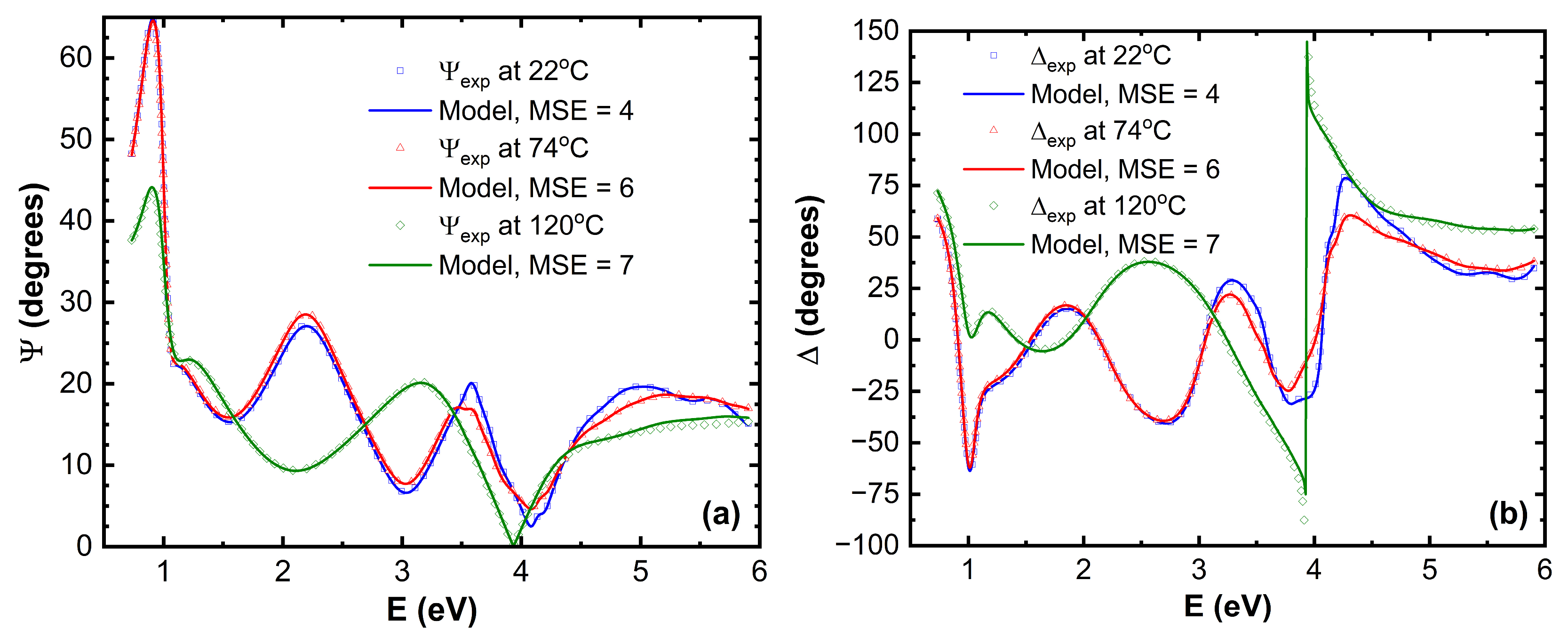
Figure 2.
Refractive index n (a) and extintion coefficient k (b) as a function of photon energy E for TAPC, CBP and BPhen compounds at room temperature.
Figure 2.
Refractive index n (a) and extintion coefficient k (b) as a function of photon energy E for TAPC, CBP and BPhen compounds at room temperature.
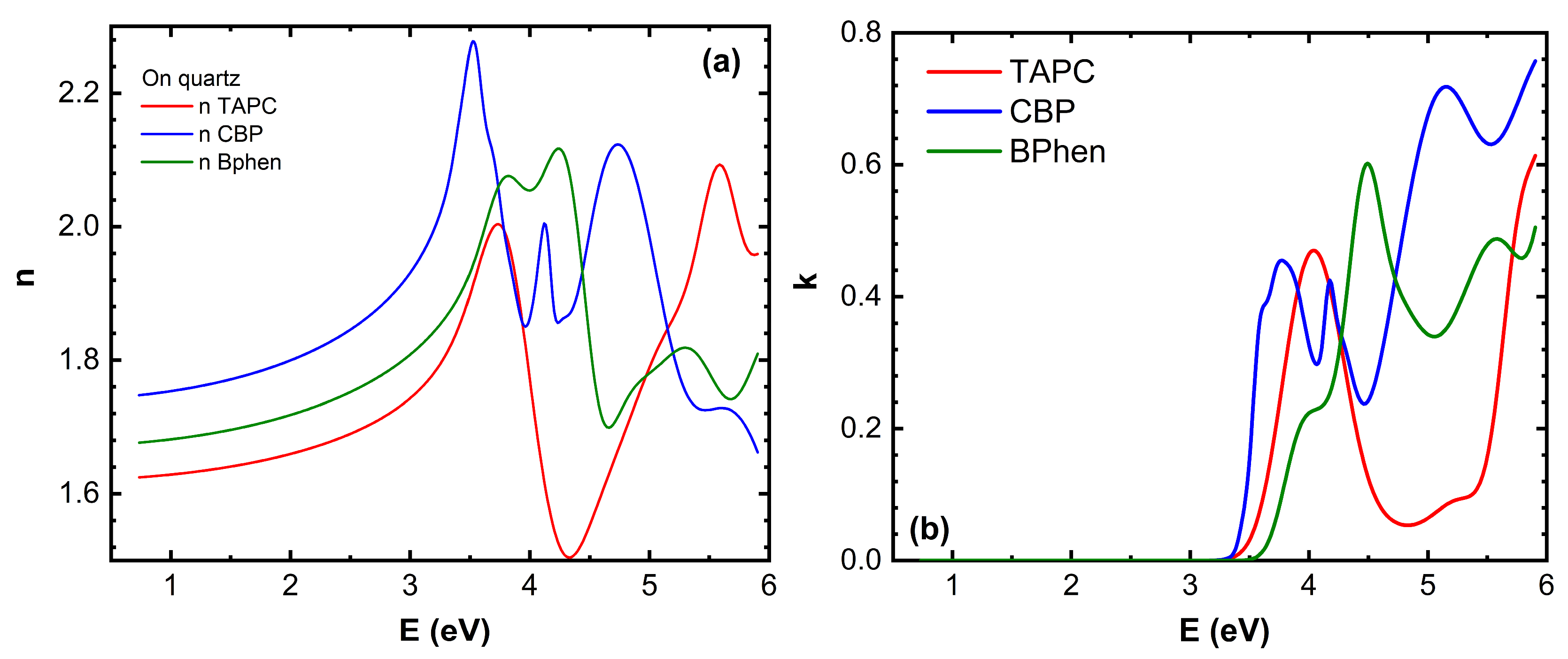
Figure 3.
Main ellipsometric angles (Ψ; Δ) as a function of temperature at photon energy 3.425 eV.
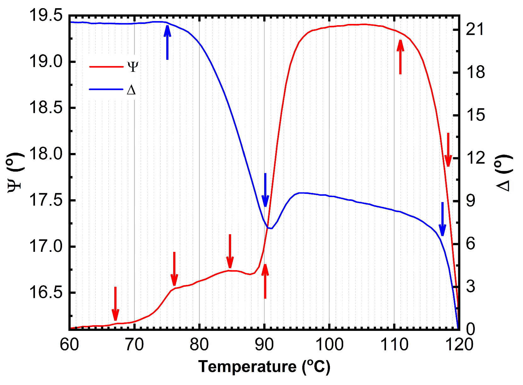
Figure 4.
Refractive index n (a) and extintion coefficient k (b) as a function of photon energy E for TAPC and BPhen compounds at room temperature and just after phase transition temperature.
Figure 4.
Refractive index n (a) and extintion coefficient k (b) as a function of photon energy E for TAPC and BPhen compounds at room temperature and just after phase transition temperature.
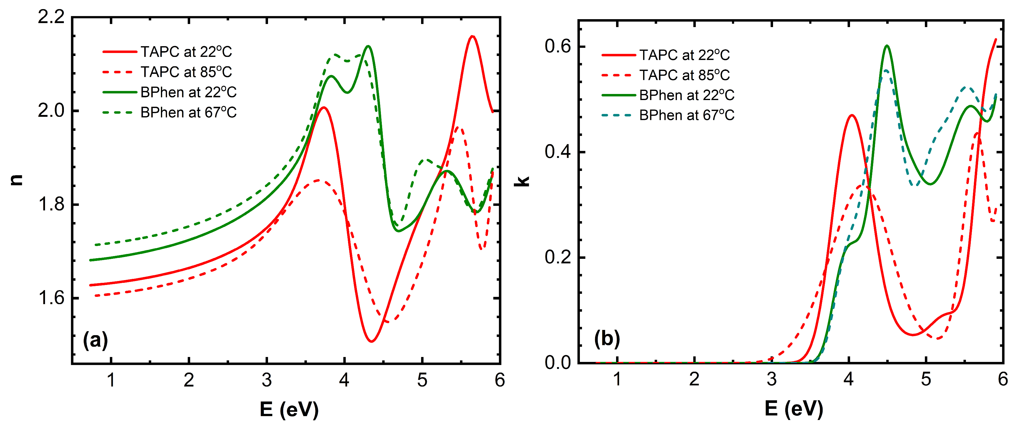
Figure 5.
Interphase layer between BPhen and CBP thin films as a function of temperature.
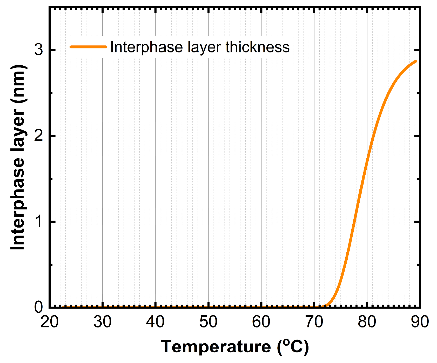
Figure 6.
The model (1) and (2) obtained results: (1) surface roughness and (2) amount of the missing film over ITO substrate as a function of temperature
Figure 6.
The model (1) and (2) obtained results: (1) surface roughness and (2) amount of the missing film over ITO substrate as a function of temperature
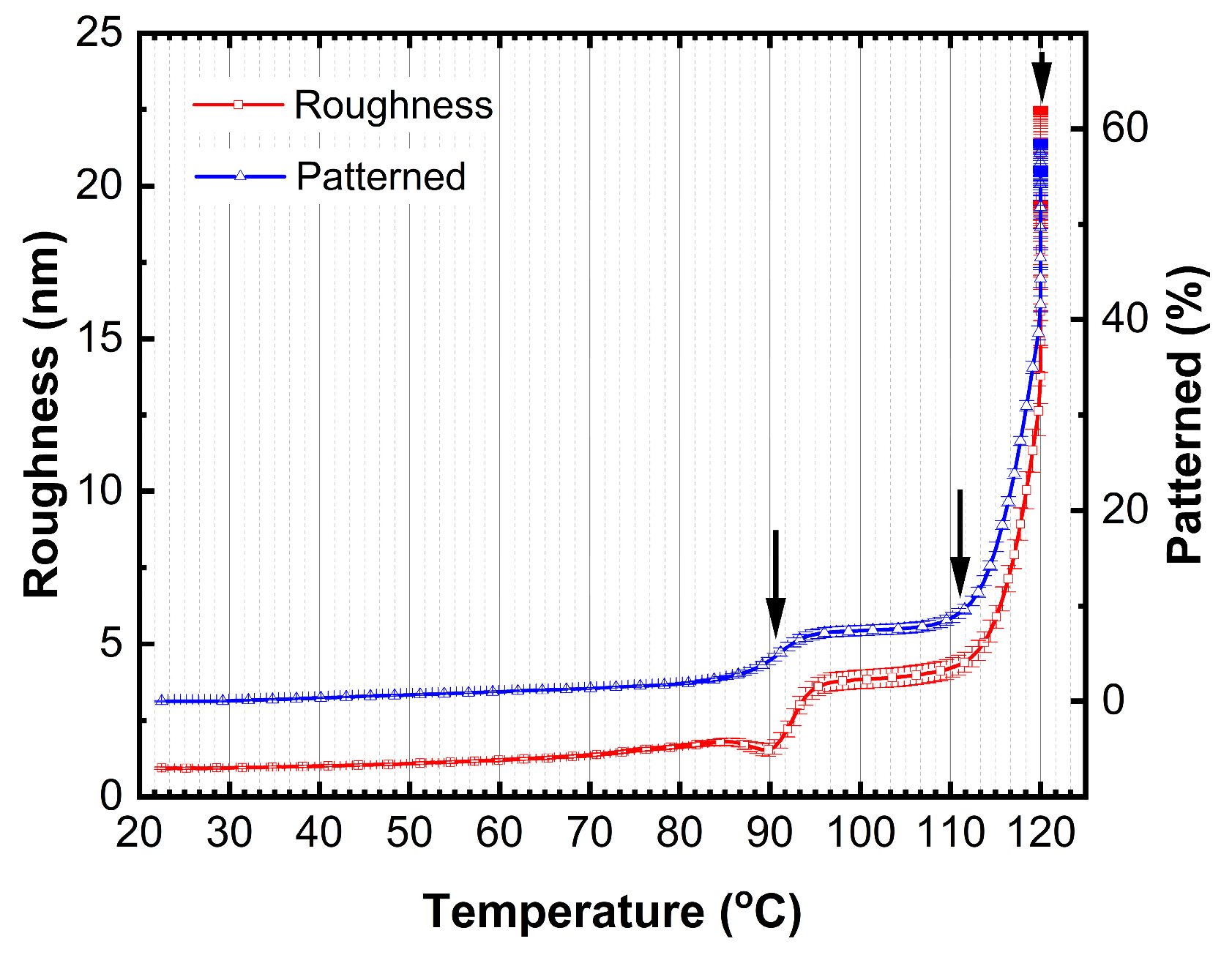
Figure 7.
Optical microscope image of the glass/SiO2 buffer/ITO/TAPC/CBP/BPhen top surface before (left) and after (right) heating.
Figure 7.
Optical microscope image of the glass/SiO2 buffer/ITO/TAPC/CBP/BPhen top surface before (left) and after (right) heating.
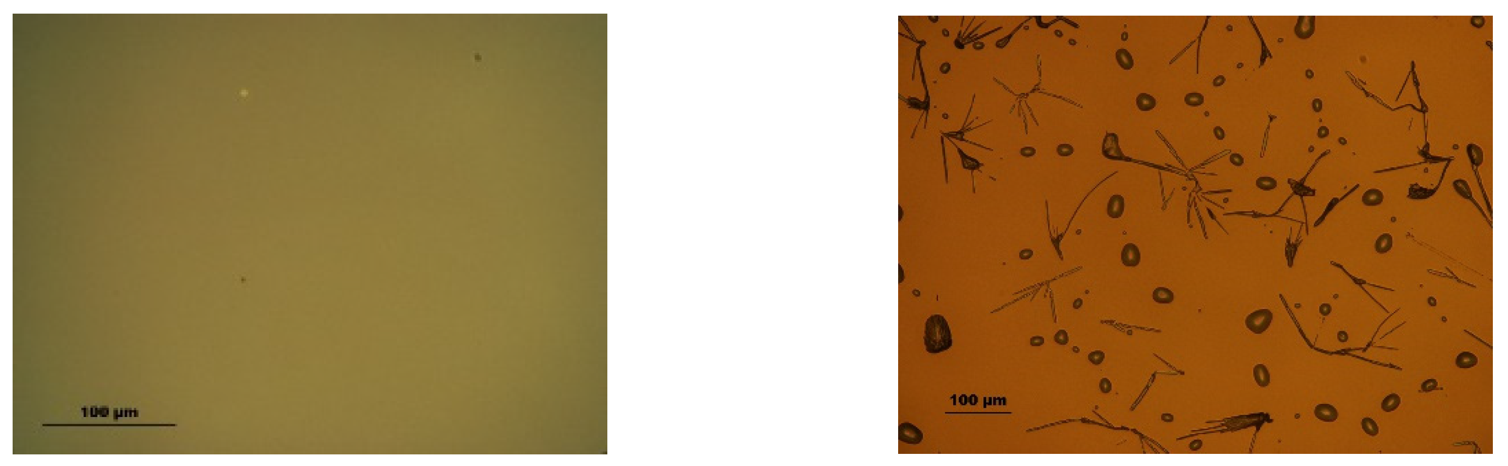
Figure 8.
AFM image of the glass/SiO2 buffer/ITO/TAPC/CBP/BPhen top surface before (left) and after (right) heating
Figure 8.
AFM image of the glass/SiO2 buffer/ITO/TAPC/CBP/BPhen top surface before (left) and after (right) heating
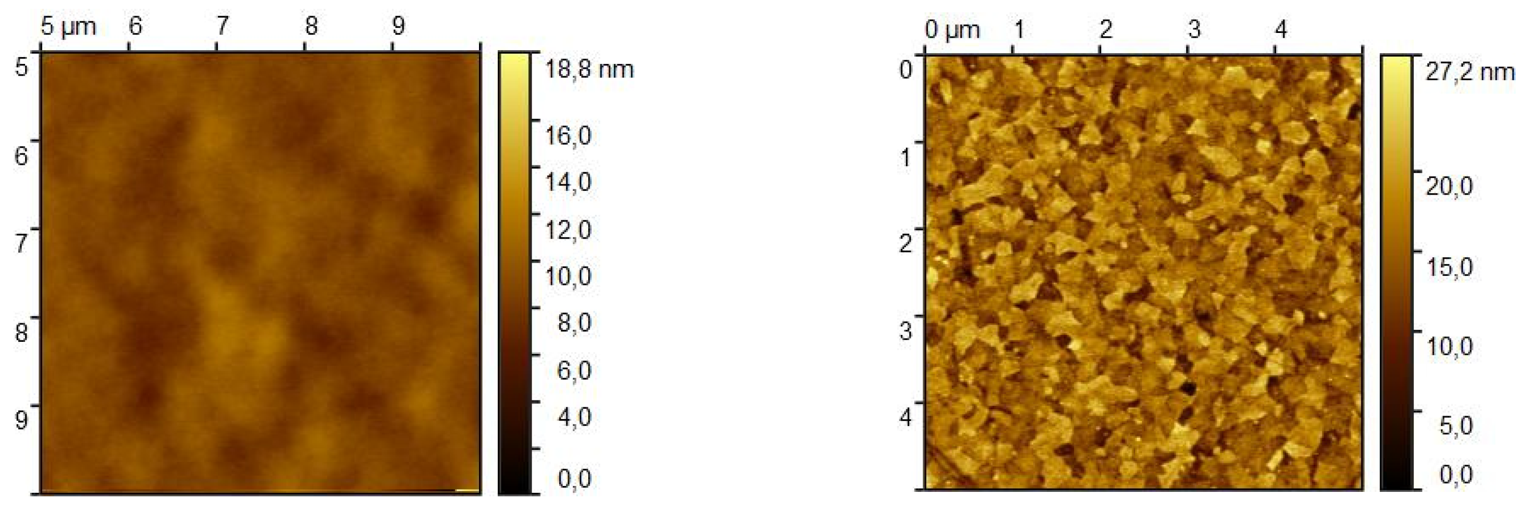
Figure 9.
The image presents a schematic illustration of the microstructural transformations occurring in the TAPC/CBP/BPhen three-layer structure deposited on an ITO substrate, as a function of temperature.
Figure 9.
The image presents a schematic illustration of the microstructural transformations occurring in the TAPC/CBP/BPhen three-layer structure deposited on an ITO substrate, as a function of temperature.
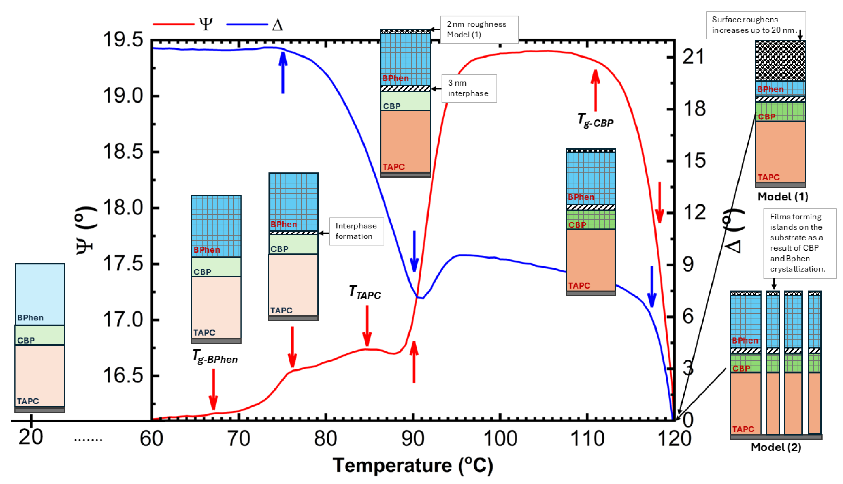

Table 1.
Temperature anomalies Ta observed in ellipsometric (Ψ; Δ) spectra: comparison with literature, sensitive parameters where Ta was observed, and the description of phase transition. The ↓↑ indicates if the sensitive parameters are increasing or decreasing at Ta.
Table 1.
Temperature anomalies Ta observed in ellipsometric (Ψ; Δ) spectra: comparison with literature, sensitive parameters where Ta was observed, and the description of phase transition. The ↓↑ indicates if the sensitive parameters are increasing or decreasing at Ta.
| Ta (°C) | Parameter | Material | Description of phase transition | |
|---|---|---|---|---|
| This work | Ref. | |||
| 66.5 ± 0.5 | 66 [7] | Ψ↑ | BPhen | Tg of BPhen |
| 76.3 ± 0.5 | - | Ψ↑, Δ↓ | - | 3 nm interphase layer creation between BPhen and CBP layers |
| 84.5 ± 0.5 | 84.5 [8] | Ψ↑, Δ↓ | TAPC | The 1st order reversible phase transition of TAPC |
| 91 ± 1 | - | Ψ↑, Δ↓, roughness ↑ | - | Increase on surface roughness due to BPhen crystallization |
| 112 ± 2 | 111.85 [9] | Ψ↓, Δ↓, roughness ↑, patterned ↑ | CBP |
Tg of CBP Shrinking of the multilayer film structure die |
Table 2.
Certain fitting parameters at specific temperatures near Ta: surface roughness Sr, BPhen, interphase, CBP, TAPC, ITO, SiO2 buffer layer thicknesses d, band gaps Eg and film patterning (amount of the film covering the ITO substrate).
Table 2.
Certain fitting parameters at specific temperatures near Ta: surface roughness Sr, BPhen, interphase, CBP, TAPC, ITO, SiO2 buffer layer thicknesses d, band gaps Eg and film patterning (amount of the film covering the ITO substrate).
| Ta | 22°C | 67°C | 77°C | 85°C | 91°C | 112°C | 120°C | |
|---|---|---|---|---|---|---|---|---|
| Parameters | ||||||||
| Sr (nm) | 0.93 ± 0.06 | 1.3 ± 0.05 | 1.6 ± 0.06 | 1.8 ± 0.1 | 1.8 ± 0.2 | (4.3 - 4.8) ± 0.3 | 21.0 ± 1.5 | |
| dBPhen (nm) | 32.54 ± 0.06 | |||||||
| dinterf (nm) | - | 0.8 ± 0.02 | 2.5 ± 0.02 | |||||
| dCBP (nm) | 9.44 ± 0.05 | |||||||
| dTAPC (nm) | 44.95 ± 0.07 | |||||||
| EgBPhen (eV) | 3.86 ± 0.02 | 3.84 ± 0.07 | ||||||
| EgCBP (eV) | 2.89 ± 0.02 | |||||||
| EgTAPC (eV) | 3.66 ± 0.02 | 3.49 ± 0.07 | ||||||
| Patterning (%) | - | 1.3 ± 0.1 | 1.6 ± 0.1 | 2.5 ± 0.2 | 5.1 ± 0.4 | (9.6 - 11.4) ± 0.5 | 57.5 ± 1.4 | |
| dITO (nm) | 102.56 ± 0.03 | |||||||
| dSiO2b (nm) | 34.50 ± 0.52 | |||||||
Disclaimer/Publisher’s Note: The statements, opinions and data contained in all publications are solely those of the individual author(s) and contributor(s) and not of MDPI and/or the editor(s). MDPI and/or the editor(s) disclaim responsibility for any injury to people or property resulting from any ideas, methods, instructions or products referred to in the content. |
© 2025 by the authors. Licensee MDPI, Basel, Switzerland. This article is an open access article distributed under the terms and conditions of the Creative Commons Attribution (CC BY) license (http://creativecommons.org/licenses/by/4.0/).
Copyright: This open access article is published under a Creative Commons CC BY 4.0 license, which permit the free download, distribution, and reuse, provided that the author and preprint are cited in any reuse.


