
Submitted:
26 November 2024
Posted:
28 November 2024
You are already at the latest version
Abstract
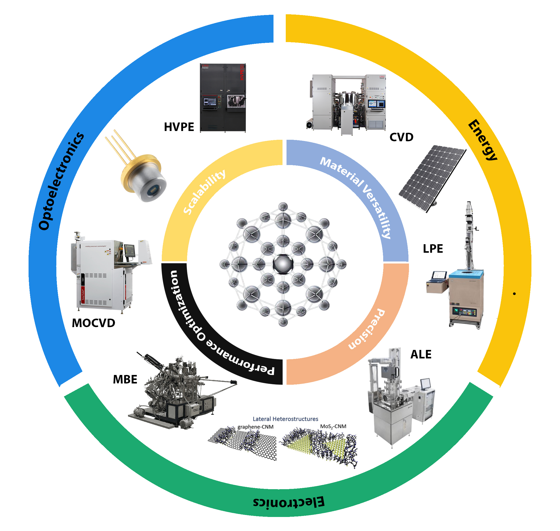
Wide-bandgap (WBG) semiconductors such as silicon carbide (SiC) and gallium nitride (GaN) play a critical role in advancing high-power and high-frequency electronic applications, including renewable energy, automotive, and telecommunications sectors. This paper provides an in-depth analysis of epitaxial growth techniques like Molecular Beam Epitaxy (MBE), Hydride Vapor Phase Epitaxy (HVPE), and Atomic Layer Epitaxy (ALE), each with unique benefits in defect control, crystal quality, and scalability. Low-energy approaches such as Hot-Filament Chemical Vapor Deposition (HFCVD) for SiC offer scalability and uniformity, addressing industrial requirements for cost-effective, high-purity substrates. The study explores advancements in AI-optimized epitaxy and hybrid growth techniques aimed at mitigating environmental impacts, such as recycling end-of-life WBG devices to minimize waste. The findings underscore the potential of these methods to drive the next generation of high-performance WBG devices and position ultrawide-bandgap (UWBG) materials like diamond and gallium oxide (Ga₂O₃) as frontrunners for extreme applications in power electronics and quantum devices.
Keywords:
wide-bandgap semiconductors
; epitaxial growth
; ultrawide-bandgap semiconductors
; molecular beam epitaxy
; sustainability
; manufacturing
1. Introduction
1.1. Overview of Wide Bandgap Semiconductors
Semiconductors are materials that have a conductivity between conductors (generally metals) and insulators (such as ceramics). Wide-bandgap (WBG) semiconductors are materials with bandgaps significantly larger than traditional semiconductors like silicon. A semiconductor is defined by its ability to conduct electricity under certain conditions such as doping, thermal and optical excitation. These conditions are significantly influenced by bandgap (Eg) – the energy difference between the conduction band minimum (the bottom of the conduction band), Ec, and the valence band maximum (the top of the valence band), Ev, expressed as E g = Ec – E v [1]. It is often expressed in electrovolts (eV). This bandgap is crucial in determining a semiconductor’s electrical, optical, and thermal properties, influencing its applications in electronics and photonics. In terms of electrical conductivity, if electrons in the valence band are provided with energy greater than the bandgap energy (from thermal energy or electrical energy), they can get excited and occupy energy levels in the conduction band, allowing them to participate in electrical conduction. For Optical properties, the bandgap determines the wavelength of light that a semiconductor can absorb or emit [2]. Photons with energy less than the bandgap cannot be absorbed, while photons with energy greater than the bandgap can excite electrons across the gap, creating electron-hole pairs. For doping, the addition of impurities changes the bandgap and Fermi level of the semiconductor, allowing control over its electrical properties [3]. Doping is essential for creating p-n junctions in devices like diodes and transistors. The relationship between doping and the energy band gap, resistivity, and mobility of semiconductors underscores the importance of doping in optimizing device performance [4]. Techniques such as selective-area doping and novel methods like photoinduced electron doping in graphene have emerged, allowing for precise control over the doping process and the creation of stable p-n junctions [5,6].
Wide-bandgap semiconductors are a class of semiconductors with bandgaps larger than 3 eV. Some examples include Silicon Carbide (SiC), Gallium Nitride (GaN), and Aluminum Nitride (AlN). These materials have higher breakdown electric fields, higher thermal conductivity, and higher maximum operating temperatures compared to traditional semiconductors like silicon (Si) and gallium arsenide (GaAs). WBG semiconductors’ larger bandgap enables them to operate at higher voltages, temperatures, and frequencies [3], making them ideal for power electronics and high-efficiency applications [7,8]. Other advantages include of WBG semiconductors also includes lower on-resistance, higher switching speed in power devices, and increased radiation hardness. Their unique properties allow for reduced energy losses and improved performance in various technologies, including renewable energy systems and electric vehicles [3,9,10], where they can improve power density and operating temperatures. The significance of WBG materials lies in their potential to enhance energy efficiency and performance in modern electronic devices [11]. However, challenges remain in terms of cost, packaging, reliability, and manufacturing that need to be addressed for widespread adoption in automotive and other industries [10]. Wider bandgaps also make it more challenging to grow high-quality crystals and achieve efficient doping. Nonetheless, WBG semiconductors are enabling new applications in power electronics, RF/microwave electronics, and optoelectronics.
Ultra-wide bandgap (UWBG) semiconductors represent a specialized category within wide-bandgap (WBG) semiconductors, characterized by even larger bandgaps than traditional semiconductors. WBG semiconductors, such as silicon carbide (SiC) and gallium nitride (GaN), possess bandgaps greater than 1.1 eV, enabling them to function effectively at elevated voltages, temperatures, and frequencies, which is a significant advantage over silicon's 1.1 eV bandgap. This capability allows WBG devices to handle higher power densities and improve thermal management, making them suitable for applications in power electronics and high-frequency communications [3,9,12]. UWB semiconductors such as Gallium Oxide (Ga2O3), β-Ga2O3, Diamond, and Aluminum Gallium Nitride (AlGaN), with bandgaps exceeding 3 eV, further enhance these properties, facilitating advancements in optoelectronics and high-temperature applications [11,13]. The increased bandgap in UWB materials not only improves efficiency but also expands the operational range, thereby addressing the limitations of traditional semiconductors in demanding environments [11,12]. The electronic properties of WBG and UWBG materials are listed in Table 1 and illustrated in Figure 1.
Proposed methods for quantifying the suitability of semiconductor materials for great potential in microelectronics applications is by the Three figure-of-merits (FOMs) which include the Johnson’s FOM (JFOM), Keyes’ FOM (KFOM), and the Baliga’s FOM (BFOM) [15,16,17,18]. JFOM is used to evaluate the suitability of semiconductor materials in high-frequency power devices, which is defined as: JFOM = where Eb is the breakdown field, and is the saturated drift velocity [17,18]. KFOM is used to evaluate the thermal limitation of the switching behavior of the semiconductor microelectronic devices, which is defined as: . , where σ is the thermal conductivity, c is the velocity of light in free space, and ε is the relative permittivity [16,18]. A simple method to quantify a device's suitability for power applications (specifically low-frequency unipolar power switching) is by the Baliga figure of merit [18] (Equation 1, Equation 2).
Or
Where;
VB is the breakdown voltage,
Ron,sp is the specific on-resistance,
ε is the permissivity,
μ is the carrier mobility, and
EG is the bandgap.
Baliga’s Figure-of-Merit (BFOM) is a crucial metric for evaluating semiconductor materials for high-power and high-frequency applications. BFOM assesses the theoretical limits of a material’s performance in terms of on-resistance and efficiency. BFOM is based on parameters like materials’ mobility (µγ), permittivity (ε γ), voltage breakdown (VB), and bandgap (EG) - (Equation 1, Equation 2). These equations are applied to compute the BFOM, which compares these materials based on the on-resistance per unit area, highlighting their suitability for high-performance power electronics. As illustrated in Figure 1(b), advanced wide-bandgap (WBG) materials, such as 4H-SiC, GaN, β-Ga2O3, AlN, and Diamond, outperform silicon (Si) in BFOM. These materials can achieve significantly higher breakdown voltages at lower on-resistance per square centimeter than Si, enhancing their power-handling capability and efficiency. This capability is critical in next-generation power converters, as it leads to reduced switching losses and conduction losses by offering higher speeds and lower on-resistances, respectively. The critical electric field strength, closely linked to the material’s bandgap, greatly influences BFOM. Materials with higher bandgaps tend to support stronger electric fields, allowing them to block higher voltages with minimal losses in the on-state. Thus, WBG materials’ superior BFOM values make them attractive for power devices, making them promising candidates for advanced power and energy applications.
1.2. Properties and Significance of Wide-Bandgap Semiconductors
Wide and ultrawide-bandgap (WBG and UWBG) semiconductors exhibit superior properties that enhance their performance in high-power applications. Their high thermal conductivity (κ) allows for efficient heat dissipation, crucial for maintaining device reliability under high currents and voltages [20]. Additionally, WBG materials like GaN and SiC possess high breakdown voltages, enabling them to operate at elevated voltages without failure, which is essential for power electronics [20,21]. The high electron mobility of these materials facilitates faster switching speeds, improving overall efficiency in electronic devices [9,21]. Applications span power electronics, RF devices, and optoelectronics, where their advantages over traditional silicon include reduced conduction losses and enhanced thermal stability [3,9]. These properties position WBG and UWBG semiconductors as pivotal in advancing modern electronic technologies.
High thermal conductivity in wide bandgap (WBG) semiconductors, such as silicon carbide (SiC) and gallium nitride (GaN), significantly enhances their performance in power electronics. This property allows for more efficient heat dissipation, which is crucial for operating at elevated temperatures and higher switching frequencies, thereby improving the overall efficiency and compactness of power conversion systems [22]. Research indicates that WBG materials with thermal conductivities exceeding 400 W/mK minimize temperature rise in power devices, which is essential for maintaining reliability and performance [23]. Furthermore, the ability to manipulate thermal properties in WBG nanowires opens avenues for advanced thermal management solutions, enhancing their application in high-performance devices [24]. However, challenges remain in packaging technologies that can fully leverage these thermal advantages, as inadequate designs may compromise device performance [25]. Overall, high thermal conductivity is a key factor that enables WBG semiconductors to outperform traditional silicon-based devices in demanding applications.
Breakdown voltage is a critical parameter in semiconductor devices, influencing device performance and reliability. It represents the maximum voltage a semiconductor can withstand before undergoing electrical breakdown, which can lead to device failure. High breakdown voltage is particularly essential in power electronics, where devices must handle significant voltages without succumbing to leakage currents or catastrophic failure. Research indicates that various structural innovations can enhance breakdown voltage. For instance, the use of trench metal-oxide-semiconductor field-effect transistors (MOSFETs) with edge termination regions effectively manages electric fields, thereby increasing breakdown voltage [26]. Additionally, materials like Gallium Nitride (GaN) exhibit superior breakdown voltage capabilities due to their larger bandgap, which allows for higher electric field strengths without breakdown [27]. Techniques such as incorporating passivation layers and optimizing defect densities in semiconductor structures also contribute to improved breakdown voltage by modifying electric field distributions and reducing leakage currents [27]. Specific designs, such as field plates and guard rings, are employed to enhance breakdown voltage in semiconductor devices. Breakdown voltage is vital for the functionality of semiconductor devices, and advancements in materials and structural designs are key to achieving higher voltage thresholds.
Electron mobility is a critical parameter in the performance of electronic devices, influencing their speed and efficiency. High electron mobility allows for faster transit times across devices, which is essential for high-frequency applications and overall device responsiveness [28]. Enhanced mobility can be achieved through various means, such as utilizing high electron mobility transistors (HEMTs) that optimize current flow between electrodes [29]. Advancements in materials like oxide heterostructures have shown promising results, with mobilities exceeding 3.5 × 106 cm²/Vs, facilitating the exploration of quantum phenomena and reducing resistance without increasing carrier density [30]. Innovative techniques, such as using light pulses to drive electron mobility in plasmonic waveguides, demonstrate the potential for significant performance improvements in electronic circuits [31]. The pursuit of high electron mobility is vital for developing next-generation electronic devices with superior performance characteristics.
Wide bandgap (WBG) semiconductors, particularly silicon carbide (SiC) and gallium nitride (GaN), are increasingly utilized in various modern technologies due to their superior performance characteristics. In the realm of electric transportation, WBG semiconductors enhance the efficiency of power converters, which are crucial for electric vehicles (EVs) by enabling high-frequency switching and reducing power losses [21]. WBG devices are integral to modern induction cookers, where they outperform traditional silicon-based semiconductors by significantly reducing power loss and enabling high power ratings and compact designs [32]. WBG materials are essential in the development of integrated circuits (ICs) for power electronics, RF systems, and optoelectronic devices, including LEDs and lasers, due to their high thermal conductivity and mobility [9]. WBG semiconductors are pivotal in advancing technologies that require high efficiency and performance under demanding conditions [33].
In general, Wide and ultrawide-bandgap (WBG and UWBG) semiconductors offer several advantages over traditional semiconductors. One major advantage is higher thermal conductivity, enabling better heat dissipation and reliability in high-temperature environments, which is crucial for power applications [34]. WBG semiconductors can operate at higher voltages and frequencies, resulting in reduced size and weight of power converters, which is particularly beneficial for electric vehicles and modern induction cookers [21,32]. Their superior electron mobility and lower on-state resistance led to decreased conduction losses, enhancing overall efficiency [21]. WBG devices demonstrate lower power loss during operation, with significant reductions in power loss compared to Si-based devices, making them more suitable for high-performance applications [32]. Despite these advantages, challenges remain in fully understanding the physics of UWBG materials, indicating a need for further research [3].
1.3. Examples of Wide-Bandgap Semiconductors
Silicon Carbide (SiC)
4H-Silicon Carbide (4H-SiC) is a prominent wide bandgap semiconductor known for its exceptional properties, making it suitable for various high-performance applications. It features a bandgap of 3.3 eV and a high breakdown field of 3.1 MV/cm, which contributes to its effectiveness in power electronic devices capable of operating at high voltages and temperatures [35,36]. The material exhibits a high saturation velocity of 2.2 × 107 cm/s and an impressive thermal conductivity of 490 W/mK, enhancing its thermal management capabilities [35]. 4H-SiC is increasingly utilized in radiation detection, particularly in harsh environments, due to its high radiation resistance and efficient charge transport mechanisms [37]. Its mechanical and acoustic properties make it an excellent candidate for Micro-Electro-Mechanical Systems (MEMS) applications [38]. The material's high melting point of 2730°C further underscores its robustness in extreme conditions [35]. 4H-SiC's unique combination of electrical, thermal, and mechanical properties (Table 1) positions it as a leading material in advanced electronic and sensor technologies.
Gallium Nitride (GaN)
Gallium Nitride (GaN) is a wide bandgap semiconductor with a bandgap of 3.4 eV, high breakdown field strength of 4.9 MV/cm, and excellent thermal conductivity of 230 W/mK, making it ideal for high-power and high-frequency applications [39,40]. GaN High Electron Mobility Transistors (HEMTs) are particularly notable for their high electron mobility and saturation velocity of 1.4 x 107 cm/s, which enables efficient operation in demanding environments such as military systems and telecommunications [40,41]. Typical applications include radio frequency amplifiers, high-voltage power electronics, and LiDAR drivers, where their ability to handle high temperatures and voltages is crucial [41,42]. Despite their advantages, GaN devices face challenges such as reliability issues and thermal management, which require advanced design and fabrication techniques [42,43]. GaN's unique properties (Table 1) position it as a leading material in next-generation electronic devices.
Aluminum Gallium Nitride (AlGaN)
AlGaN (Aluminum Gallium Nitride) is a semiconductor material known for its wide bandgap, typically ranging from 3.4 eV to over 4 eV depending on the aluminum content, which makes it suitable for high-power and high-frequency applications [44,45]. It exhibits a high breakdown field (up to 3 MV/cm), enabling devices to operate under extreme conditions [46]. The saturation velocity of AlGaN is notably high, reaching values around 2.5 x 107 cm/s, which is advantageous for fast electronic devices [45]. AlGaN has good thermal conductivity, making it effective for heat dissipation in power electronics [45]. Typical applications of AlGaN include high electron mobility transistors (HEMTs) used in RF power amplifiers, optoelectronic devices, and sensors, particularly in military and telecommunications sectors due to their robustness and efficiency [40,47]. The material's melting point is approximately 2000°C, and it has demonstrated compatibility with CMOS technology, although challenges remain in thermal budget management [45]. AlGaN's unique properties position it as a critical material in advancing modern electronic and optoelectronic devices.
Diamond
Diamond is a remarkable semiconductor material characterized by its ultra-wide bandgap of approximately 5.5 eV, high thermal conductivity (up to 2200 W/m·K), and exceptional mechanical properties, including the highest hardness and Young's modulus. These properties make diamond suitable for high-power and high-frequency applications, such as Schottky barrier diodes (SBDs) and field-effect transistors (FETs) in power electronics, where it can handle high breakdown fields (up to 20 MV/cm) and high current densities (60 kA/cm²) [48,49]. Diamond's unique characteristics (Table 1) enable its use in optoelectronic devices, including ultraviolet detectors and sensors, due to its high optical transmittance and exciton binding energy [50]. One-dimensional diamond nanostructures exhibit enhanced properties, making them ideal for applications in micro/nano-electromechanical systems (MEMS/NEMS) and quantum technologies [51,52]. Despite challenges in doping for n-type conductivity, ongoing research continues to explore innovative applications and device structures for diamond [48].
Gallium Oxide (Ga2O3)
Gallium Oxide (Ga2O3) is an ultrawide-bandgap semiconductor with a bandgap ranging from 4.5 to 4.9 eV, making it suitable for high-power and high-voltage applications due to its ability to withstand high breakdown fields (up to 10.3 MV/cm) and elevated temperatures [53,54]. Its high saturation velocity (1.8 × 107 cm/s) and thermal conductivity (13 W/mK) further enhance its performance in electronic devices [54,55]. Ga2O3 is particularly promising for power electronics, including high-voltage rectifiers and inverters, due to its superior Baliga's figure of merit (BFOM) of 4125 (Table 1), which is significantly higher than that of silicon and other semiconductors [54,56]. Ga2O3 is being explored for optoelectronic applications, such as UV photodetectors and neuromorphic computing, leveraging its sensitivity to UV-C light and resistive switching properties [55,57]. However, challenges remain, particularly in achieving effective p-type doping and managing thermal limitations [57].
1.4. Overview of Epitaxial Growth Techniques
Epitaxial growth is a critical process in synthesizing high-quality wide bandgap (WBG) semiconductor materials, enabling the precise layering of materials with controlled properties. This process involves depositing a thin layer of crystalline material on a substrate, where the deposited layer's crystal structure closely matches that of the substrate [1,58]. This alignment is essential for achieving desired electronic and optical properties in the resulting materials, making epitaxial growth vital for applications in electronics, optoelectronics, and photonics. The epitaxial growth process enables the growth of few impurity layers compared to bulk materials, enhancing electrical performance [1]. The technique allows for the introduction of dopants in specific concentrations, essential for tailoring device characteristics [3,58]. By using different materials for the epitaxial layer compared to the substrate, engineers can create devices with unique properties, such as lasers and LEDs [1,59]. The smooth interfaces achieved through epitaxial growth improve charge carrier mobility, leading to better device performance [1,58].
The two main categories of epitaxial growth are Homoepitaxy and Heteroepitaxy. Homoepitaxy involves the growth of a semiconductor layer on a substrate of the same material (e.g. doped Si on Si), ensuring high crystallographic quality. This method is often employed when a specific thickness or material quality is needed. It allows for the growth of a layer of the same material, enhancing the substrate’s properties without introducing new materials that could lead to defects or impurities. One advantage of this type of epitaxy growth is better control over doping and defect density, crucial for high-performances devices [60]. Heteroepitaxy is the epitaxial growth of a deposit on a substrate of a different material (Au on Ag, GaAs on Si). This technique can lead to challenges due to lattice mismatches. This technique enables the creation of structures with unique material combinations, which can be beneficial for developing advanced semiconductor devices. Recent advancements include metal-seeded epitaxial growth, enabling the formation of noble metal-semiconductor heterostructures despite significant lattice mismatches [61].
Epitaxial growth modes are critical for the development of semiconductor materials, particularly in thin-film applications. The primary modes include Frank-van der Merwe (FM), Stranski-Krastanov (SK), and Volmer-Weber (VW), each characterized by distinct mechanisms and conditions. The Frank-van der Merwe (FM) Mode involves layer-by-layer growth, where each atomic layer is completed before the next begins. This mode is favored when there is minimal lattice mismatch between the substrate and the film, promoting high-quality epitaxy [62]. The Stranski-Krastanov (SK) Mode is a hybrid approach where an initial layer grows in a two-dimensional manner, followed by three-dimensional island formation. This mode is often observed in quantum dot fabrication, particularly in semiconductor applications, due to its ability to accommodate strain [63]. In Volmer-Weber (VW) Mode, growth occurs via island formation without a continuous layer, typically under conditions of significant lattice mismatch. This mode can lead to lower-quality films but is useful for specific applications where such structures are desired [62]. While these modes provide a framework for understanding epitaxial growth, advancements in techniques like droplet epitaxy and laser-assisted growth are expanding the possibilities for controlling these processes [63,64].
The main epitaxial growth techniques include Molecular Beam Epitaxy (MBE), Metal-Organic Chemical Vapor Deposition (MOCVD), and Hydride Vapor Phase Epitaxy (HVPE), each with unique principles and applications. Molecular Beam Epitaxy (MBE) utilizes molecular beams in ultra-high vacuum to deposit layers [65]. It is a highly controlled method where materials are vaporized in a vacuum and directed towards a substrate[66]. The atoms or molecules condense on the substrate, forming layers. Ideal for high-purity materials and precise control over thickness [67] as it ensures minimal contamination and allows precise control over thickness and composition. This technique is widely used for producing complex semiconductor structures, including quantum wells and superlattices [68,69]. Metal-Organic Chemical Vapor Deposition (MOCVD) employs metal-organic precursors in a vapor phase, suitable for large-area coatings and complex structures [65]. It involves the chemical reaction of metal-organic precursors in a heated chamber, leading to the deposition of thin films. This method is characterized by higher growth rates as it is faster than MBE, making it suitable for industrial applications. The method is versatile as it can deposit a wide range of materials, including compound semiconductors [70]. This technique is commonly used for producing LEDs, laser diodes, and solar cells [69,70]. Hydride Vapor Phase Epitaxy (HVPE) involves utilizing gas-phase reactions such as hydride gases to grow epitaxial layers, effective for growth thick layers of III-V semiconductors or WBG materials like GaN [65,69,70]. Its advantages include high growth rates as it is capable of producing thick layers quickly [70] and it is particularly effective for growing GaN layers on foreign substrates. This technique is used in high-power electronics and optoelectronic devices.
Other Techniques include Liquid Phase Epitaxy (LPE) and Atomic Layer Epitaxy (ALE). Liquid Phase Epitaxy (LPE) involves the deposition from a molten solution, suitable for growing thick layers but with challenges in uniformity. Atomic Layer Epitaxy is a variant that allows for atomic-scale control of thickness through sequential gas-phase reactions. LPE involves depositing layers from a molten solution, typically at high temperatures (up to 1200OC), allowing for rapid growth and low defect densities. It is particularly effective for III-V compound semiconductors, used in devices like LEDs and photovoltaic cells. Despite its advantages, LPE is less effective for ultrathin layers and precise interfaces compared to methods like MBE and MOCVD [71]. ALE’s precision and versatility position it as a more favorable choice for advanced semiconductor technologies. However, the complexity and cost of ALE processes can be a barrier for some applications, suggesting a balanced approach may be necessary in material selection. Techniques like Plasma Enhanced Atomic Layer Deposition (PEALD) expand the range of materials and processing conditions, improving film properties significantly [72].
The fundamental theories behind Epitaxial Growth include Lattice Matching and Epitaxial Strain. Lattice Matching is essential for successful epitaxial growth ensuring minimizing defects [73], where the lattice constant (asub) of the substrate and the epitaxial layer (aepi) must be closely aligned. The strain (ε) resulting from lattice mismatch can be quantified using the equation:
Equation 3 indicates that when the lattice constants differ strain can lead to defects, impacting the material’s electronic properties [74]. Strain can affect electronic properties, necessitating careful control during growth [73]. While epitaxial growth techniques are pivotal for high-quality semiconductor fabrication, challenges such as strain management and material defects remain critical areas for ongoing research and development.
1.5. Challenges in Epitaxial Growth of WBG Semiconductors
The epitaxial growth of wide-bandgap (WBG) semiconductors, such as GaN, SiC, and β-Ga2O3, faces several significant challenges that directly impact device performance and reliability. These challenges include managing defect density, stress and strain, uniformity, scalability, and the presence of dislocations and stacking faults. Each factor plays a critical role in determining the quality of the semiconductor material and, consequently, the efficiency and longevity of the devices made from them.
Defect density is a primary concern in the epitaxial growth of WBG semiconductors. High defect densities can lead to reduced carrier mobility, increased leakage currents, and diminished overall device performance. For example, GaN grown on sapphire substrates often exhibits defect densities ranging from 109 to 1010 dislocations per cm², while SiC typically shows around 103 dislocations per cm². High defect densities, such as the reported 9.2 × 10⁷ dislocations/cm² in GaSb-on-silicon substrates, can severely degrade electronic properties and lead to device failure [75]. Such high defect levels can severely hinder the performance of power devices, which are crucial for high-voltage applications. Transition-metal dichalcogenides (TMDs) also face challenges in controlling defect density, impacting their electronic and optical performance [76].
Effective management of stress and strain during epitaxial growth is critical, as mismatches between the thermal expansion coefficients and lattice parameters of the substrate and epitaxial layer can induce significant stress. This stress often leads to the formation of dislocations and other defects [77,78]. The critical thickness (hc) for a given material, determined by the equation hc = , where b is the Burgers vector and ϵ is the mismatch strain, highlights the importance of maintaining strain within acceptable limits to prevent defect formation [75]. Additionally, understanding Poisson’s ratio (ν) is essential for assessing how lateral and axial strains interact, influencing the mechanical stability of the epitaxial layers.
Uniformity in epitaxial layers is vital for fabricating reliable devices. Achieving uniform growth across large areas remains a challenge, particularly for organic semiconductors, where substrate defects can disrupt growth [79]. Variations in thickness, composition, and defect density across the wafer can lead to inconsistent device performance. Scalability presents another challenge, as processes that work well on smaller scales may not translate effectively to larger substrates. For example, achieving uniformity in AlGaN layers is critical for high-performance transistors, but ensuring this on larger wafers remains a significant hurdle [77]. The phase-selective epitaxy of bismuth thin films further underscores the importance of substrate quality in achieving uniformity and desired phase characteristics [80].
Dislocations and stacking faults significantly impact the performance of epitaxial layers, particularly in GaN-based devices. Dislocations can serve as recombination centers, while stacking faults disrupt the crystal structure, both leading to reduced efficiency and reliability in applications like LEDs and power transistors. Dislocations in GaN can lower breakdown voltage and increase leakage currents, which are critical for high-voltage applications [81]. The formation of V-defects from threading dislocations can enhance carrier injection in LEDs, but an optimal density is necessary to balance performance [82]. Stacking faults in GaN reduce the band gap, which can degrade electronic properties and affect device efficiency [83]. These faults can also introduce nontrivial electronic states, potentially altering conductivity and electronic behavior in materials [84]. While dislocations and stacking faults are detrimental, they can also be engineered to create beneficial electronic states, suggesting a dual role in material performance.
Different wide bandgap (WBG) semiconductors, including GaN, SiC, and β-Ga2O3, face distinct challenges primarily related to their material properties, which impact their performance in electronic applications. GaN exhibits high defect density when grown on sapphire substrates, leading to reliability issues in devices [42]. Ongoing research aims to develop GaN-on-GaN structures to mitigate defects, but achieving high-quality epitaxy remains a significant challenge [2]. SiC, while having lower defect densities, struggles with achieving uniform doping, which is crucial for high-power applications [85]. Managing thermal properties is essential, as SiC devices operate under high temperatures, necessitating effective heat dissipation strategies [21]. β-Ga2O3 shows potential for high-voltage applications, yet controlling the growth process to minimize dislocations and achieve high-quality films is a major challenge [3].
Defects in wide bandgap (WBG) semiconductors significantly impact device performance across various parameters, including carrier mobility, leakage currents, breakdown voltage, and thermal stability. Understanding these effects is crucial for optimizing device design and functionality. High defect densities, such as dislocations, can severely reduce carrier mobility, which diminishes the current drive capabilities of power devices [86]. In Ga2O3 power diodes, the presence of electron traps linked to defects leads to fluctuations in carrier transport, further impairing mobility [86]. Increased dislocation density correlates with higher leakage currents, particularly in high-voltage applications where efficiency is critical [86]. The shallow traps identified in Ga2O3 diodes contribute to premature breakdown and increased leakage, highlighting the need for effective defect management [86]. Dislocations serve as recombination centers, lowering the breakdown voltage and limiting operational capabilities [86]. The study on Ga2O3 diodes shows that controlling trap densities can enhance breakdown characteristics, emphasizing the importance of defect engineering [86]. Defects adversely affect thermal stability, which is vital for performance in high-temperature environments [87]. Research indicates that high temperatures exacerbate defect-related issues, leading to significant performance degradation in devices like super-junction Insulated Gate Bipolar Transistors (IGBTs) [87]. While defects pose challenges, advancements in defect engineering and material optimization can mitigate these impacts, enhancing the reliability and efficiency of WBG semiconductor devices.
1.5. Objectives of the Research
The primary objective of this review paper is to critically analyze the synthesis methods, challenges, and prospective technological innovations related to the epitaxial growth techniques for WBG semiconductors. The paper is structured as follows: Section 1 provides a comprehensive overview of WBG semiconductors and their significance in modern technology and an introduction on epitaxial growth. Section 2 focuses on the epitaxial growth techniques, discussing their principles, advantages, and limitations. We explore the challenges associated with these growth methods, such as strain management and interface engineering. Section 3 delves into the applications of epitaxially grown WBG semiconductors. Section 4 critically analyzes current innovations and future research directions, identifying potential breakthroughs that could revolutionize WBG semiconductor technology. Finally, Section 5 summarizes the findings and offers concluding remarks on the future of WBG semiconductors in advanced applications.
2. Epitaxial Growth Techniques
2.1. Molecular Beam Epitaxy (MBE)
Molecular Beam Epitaxy (MBE) is a sophisticated physical vapor deposition technique that enables the fabrication of semiconductor materials with atomic precision, allowing meticulous control over layer thickness and composition. MBE operates in ultra-high vacuum conditions, which are essential for precisely regulating the composition and morphology of deposited layers, thus optimizing the electronic and optoelectronic properties of the materials. This process involves the deposition of atoms or molecules from a vapor phase onto a substrate in a high-vacuum environment, allowing for the creation of high-quality crystalline structures with minimal defects [67].
MBE allows for the growth of layers with atomic-layer control, enabling the creation of structures with abrupt interfaces and tailored doping profiles [66]. This method is particularly advantageous for fabricating complex semiconductor heterostructures, as it enables the engineering of band gaps and doping profiles essential for wide bandgap (WBG) semiconductors. This method is particularly effective for growing high-quality wide-bandgap semiconductors (WBGs) such as Gallium Nitride (GaN), Silicon Carbide (SiC), and Aluminum Gallium Nitride (AlGaN) [88,89]. These materials have wide bandgaps, high breakdown fields, and high electron saturation velocities, making them ideal for high-power, high-frequency, and high-temperature electronic devices [89].
MBE's applications extend to the growth of materials like germanium on sapphire, where careful control of film thickness significantly influences surface morphology and crystal quality [90]. One Key feature of MBE is the use of Reflection High-Energy Electron Diffraction (RHEED) for real-time growth monitoring, enabling precise adjustments during deposition to maintain optimal conditions for layer formation[68]. While MBE is highly effective for semiconductor fabrication, it requires meticulous control and can be resource-intensive, which may limit its scalability for mass production compared to other deposition techniques.
MBE Technique Process
Molecular Beam Epitaxy (MBE) is a highly specialized epitaxial growth technique widely employed in the semiconductor industry for creating advanced materials with atomic precision. Operating under ultra-high vacuum (UHV) conditions, typically between 10−8 and 10−12 Torr, MBE provides a contamination-free environment, allowing for the deposition of ultra-pure thin films. This high vacuum environment ensures minimal contamination, enabling the growth of materials with precise control over thickness, composition, and doping profiles, which is essential for advanced electronic and optoelectronic applications [91,92].
In MBE, high-purity materials such as gallium and arsenic are heated in effusion cells or electron-beam evaporators until they sublime, creating atomic or molecular beams. These beams travel through the vacuum chamber and condense onto a carefully heated crystalline substrate, where they adhere and form epitaxial layers one atomic layer at a time [66]. This level of control allows for the fabrication of sophisticated structures with atomically smooth, abrupt interfaces and tailored doping profiles at nanometer scales. The schematic diagram of MBE is shown in Figure 2. The growth mechanisms in MBE enable the formation of two-dimensional thin films, one-dimensional nanorods, and zero-dimensional quantum dots, which are capable of complete carrier confinement on both lattice-matched and lattice-mismatched substrates [93].
The MBE process is governed by several kinetic processes, including adsorption, desorption, surface diffusion, migration, incorporation, and decomposition of reactive atoms or molecules on the heated substrate [93]. These processes allow for precise, real-time control over the film growth, ensuring high-quality, clean interfaces, and enabling the fabrication of complex semiconductor heterostructures with minimal defects. This precise control over atomic-layer growth makes MBE particularly effective for wide bandgap (WBG) semiconductors such as Gallium Nitride (GaN), Silicon Carbide (SiC), and Aluminum Gallium Nitride (AlGaN), which exhibit wide bandgaps, high breakdown fields, and high electron saturation velocities, making them suitable for high-power, high-frequency, and high-temperature devices.
MBE’s high level of precision is further supported by real-time monitoring techniques such as Reflection High-Energy Electron Diffraction (RHEED). RHEED provides feedback on surface structure and growth rates, allowing for adjustments to beam intensities and substrate temperature to optimize layer formation. This monitoring capability is invaluable for maintaining the rigorous standards needed for next-generation semiconductor devices [68].
MBE’s unique ability to control composition and doping profiles at the nanoscale has made it indispensable for research in nanoelectronics and optoelectronics. The technique supports the growth of two-dimensional layers with atomically smooth interfaces, as well as one-dimensional and zero-dimensional structures like nanorods and quantum dots, which are vital for developing novel semiconductor-based devices with enhanced performance at the nanoscale [93]. Despite MBE’s unmatched precision and high-quality output, its complex control requirements and resource-intensive nature can limit scalability for mass production compared to other deposition techniques.
MBE advantages, applications, and challenges
Molecular Beam Epitaxy (MBE) offers several advantages as it is a sophisticated technique pivotal for the growth of high-quality epitaxial films, particularly in the realm of advanced electronic and optoelectronic devices. It operates under ultra-high vacuum conditions, which significantly reduce contamination and enable the creation of defect-free layers with precise atomic control over thickness and composition [94]. MBE's advantages also include its suitability for low-temperature processes, which mitigate autodoping issues, and its ability to fabricate complex structures such as quantum wells and superlattices, essential for III-V semiconductors and wide-bandgap materials like GaN [68,69].
However, despite its advantages, MBE faces notable challenges. Its growth rate, typically between 0.01 and 0.3 μm/min, is considerably slower than other deposition methods, which limits scalability and large-scale production. The necessity for costly ultra-high vacuum systems further adds to its limitations, requiring meticulous maintenance to avoid contamination or pressure fluctuations that could degrade film quality. Achieving uniform growth, especially in complex materials, can also be challenging due to surface reactions that complicate the process, and any surface contamination or structural defects can compromise the epitaxial layer’s performance [95].
Despite these limitations, MBE remains vital in semiconductor fabrication and research. It plays a crucial role in the development of semiconductor devices such as light-emitting diodes (LEDs), lasers, solar cells, and high-electron-mobility transistors (HEMTs). The technique is also particularly effective for wide-bandgap semiconductors like Gallium Nitride (GaN) and Silicon Carbide (SiC), which are essential in high-power and high-frequency applications. MBE’s ability to create high-purity heterostructures makes it invaluable in advanced research areas, including nanotechnology and quantum computing, where precise control over material properties is critical [94,95]. As the demand for high-performance electronic devices continues to grow, MBE remains a foundational technique, driving both industrial and academic advancements in semiconductor technology and material science.
2.2. Chemical Vapor Deposition (CVD) or Epitaxial Chemical Vapor Deposition (E-CVD)
Chemical Vapor Deposition (CVD) is a versatile technique employed for the deposition of thin films and nanostructures, crucial in various technological applications such as electronics and photovoltaics. CVD operates through chemical reactions in the vapor phase, allowing for precise control over film properties, which is essential for enhancing the quality and uniformity of the deposited materials [96,97]. Variants like Plasma-Enhanced CVD (PECVD) and Hot-Filament CVD (HFCVD) are particularly notable for their effectiveness in growing materials such as diamond and silicon carbide (SiC). For instance, microwave plasma CVD has been shown to achieve high nucleation densities for diamond films on SiC substrates, significantly improving film quality through optimized parameters like methane concentration and substrate temperature [98].
PECVD enhances the traditional CVD process by utilizing plasma energy to drive the chemical reactions at lower temperatures compared to thermal CVD methods. This technique is particularly advantageous when working with temperature-sensitive substrates or when specific film properties are required. HFCVD employs a heated filament to thermally decompose precursor gases, facilitating the deposition of materials like diamond. This method is known for its simplicity and cost-effectiveness.
Furthermore, advancements in CVD technology continue to evolve, enabling the synthesis of high-purity thin films, including 2D materials, while addressing challenges related to process control and scalability [99].
Chemical Vapor Deposition Process
Chemical vapor deposition (CVD) is a sophisticated process where vapor-phase precursors react chemically on or near a heated substrate, leading to the deposition of solid films. The process typically involves three stages: heating, reaction, and cooling. Initially, the reaction chamber is heated to a predetermined temperature, facilitating the vaporization of precursors. During the reaction stage, these precursors undergo surface reactions, diffusion, and desorption, with temperature control being crucial for uniform film thickness and quality [96]. The deposition occurs at high temperatures (900–1400 °C) under low pressure, optimizing the Gibbs free energy for solid formation [96,100]. Various reactor designs, such as hot-wall and plasma-enhanced CVD (PECVD), utilize different heating methods, including resistive heating or plasma sources, to enhance deposition rates and material properties [99].
In PECVD, plasma energy is utilized to enhance chemical reactions at lower temperatures compared to traditional thermal CVD methods. The plasma is generated using radio frequency (RF) energy, which ionizes the precursor gases and creates reactive species that facilitate film deposition. HFCVD employs a heated filament to decompose precursor gases. The filament serves as a catalyst, allowing for efficient breakdown of gases at high temperatures while maintaining lower temperatures at the substrate level. This differential temperature promotes uniform deposition of materials such as diamond and silicon carbide. A schematic diagram pf PECVD and HFCVD is shown in Figure 3.
Overall, CVD remains pivotal in producing high-quality thin films for diverse applications, including semiconductors and advanced materials [100].
CVD Advantages, Applications, and Challenges
Chemical Vapor Deposition (CVD) techniques offer significant advantages in semiconductor manufacturing, particularly in the growth and fabrication of high-quality thin films. CVD allows for precise control over film composition and thickness, enabling the production of materials with tailored properties essential for advanced applications such as 2D materials and polymeric films [99]. The method's scalability and repeatability make it suitable for industrial applications, including solar cells and water filtration systems [102]. Specific CVD variants, such as Plasma-Enhanced CVD (PECVD), enhance deposition rates and allow for lower temperature processing, which is crucial for temperature-sensitive substrates. Hot-filament CVD, on the other hand, provides improved film adhesion and uniformity, making it advantageous for complex geometries in semiconductor devices [103]. Other variants of CVD include Low-Pressure CVD, High-Temperature CVD, and Atomic Pressure CVD. A comparison of the variant CVD is shown in Table 2.
CVD techniques are integral to advancing semiconductor technology through their versatility and efficiency. A comparison of the variant CVD is shown in Table 2.
Plasma-enhanced chemical vapor deposition (PECVD) and hot-filament chemical vapor deposition (HFCVD) are pivotal techniques in the growth of semiconductor materials like diamond and silicon carbide (SiC), which are essential for high-performance power electronics. Diamond, with its ultra-wide bandgap (5.47 eV) and exceptional thermal conductivity, is particularly promising for high-power applications, including Schottky barrier diodes and field-effect transistors (FETs) that can operate at elevated temperatures [49,104]. HFCVD has shown significant advancements in producing single-crystal diamonds, achieving growth rates over 10µm/h while addressing challenges such as filament contamination and doping for improved crystallinity [105]. SiC, another critical material, is recognized for its high breakdown voltage and thermal stability, making it suitable for high-voltage applications [106]. Both materials are at the forefront of research aimed at enhancing device performance and reliability in demanding environments [106].
Chemical Vapor Deposition (CVD), including its variants like PECVD and HFCVD, faces several significant challenges that impact its efficacy and cost-effectiveness. One major issue is the high cost of precursors, which can limit the scalability of processes, particularly in applications like integrated circuits where cost efficiency is crucial [107]. Additionally, achieving uniformity in film deposition remains problematic due to the complex interactions between gas-phase reactions and surface reactions, which can lead to variations in film quality and properties [108,109]. Precise temperature control is also essential, as deviations can trigger unwanted chemical reactions, adversely affecting the desired film characteristics. The opaque nature of CVD reactors further complicates the understanding of these processes, making it difficult to optimize conditions for consistent results [109]. Thus, addressing these challenges is vital for advancing CVD technologies.
2.3. Metal-Organic Chemical Vapor Deposition (MOCVD)
Metal-Organic Chemical Vapor Deposition (MOCVD) is a critical chemical process utilized for the deposition of thin layers of semiconductor materials, particularly in the mass production of compound semiconductors like Gallium Nitride (GaN) and transition metal dichalcogenides (TMDs). This technique allows for precise control over growth conditions, including precursor flux and reactor geometry, which are essential for achieving high-quality thin films with uniformity and desired properties [110]. MOCVD is particularly advantageous due to its ability to operate at high temperatures and under chalcogen overpressures, facilitating the epitaxial growth of monolayers and heterostructures. The process is widely adopted in the semiconductor industry, especially for applications in optoelectronic devices, where the quality of the thin films directly impacts device performance and reliability [110,111]. MOCVD stands out as one of the most prevalent techniques for the scalable production of advanced semiconductor materials [112].
MOCVD Technique Process
The Metal-Organic Chemical Vapor Deposition (MOCVD) process for depositing Gallium Nitride (GaN) involves critical gas-phase chemical reactions between metal-organic precursors, such as trimethylgallium (TMG), and hydrides like ammonia (NH3). In the reactor, TMG decomposes to release gallium, while NH3 provides nitrogen, facilitating the formation of GaN on a heated substrate. The efficiency of these reactions is influenced by the flow rates of TMG and NH3, as well as the carrier gas composition, typically a mixture of hydrogen and nitrogen, which enhances deposition rates and film uniformity [110,111]. The reactor's design and operating conditions, including pressure and temperature gradients, play a significant role in optimizing the growth process and minimizing impurities [113]. A typical MOCVD reactor includes a gas inlet for precursors, a substrate holder for the heated substrate, and an exhaust system for byproducts, ensuring effective material deposition and removal of excess gases. The schematic diagram of MOCVD is shown in Figure 4.
MOCVD Advantages, Applications and Challenges
Metal-Organic Chemical Vapor Deposition (MOCVD) offers significant advantages in the production of materials such as GaN, AlGaN, and InGaN, particularly for applications in LEDs and solar cells. MOCVD's high throughput is facilitated by advanced reactor designs, such as the multi-wafer systems that allow simultaneous processing of multiple substrates, enhancing uniformity and deposition rates while minimizing impurities [110,115]. The scalability of MOCVD enables effective transitions from laboratory research to large-scale production, ensuring consistent device performance across various manufacturing stages [116]. MOCVD's versatility allows for the deposition of diverse materials on different substrates, crucial for complex structures like multi-junction solar cells, while in situ monitoring capabilities ensure precise control over growth conditions, thereby supporting advancements in semiconductor technology [111]. This combination of high throughput, scalability, and versatility solidifies MOCVD's role as an indispensable method in the semiconductor industry.
Metal Organic Chemical Vapor Deposition (MOCVD) plays a crucial role in the growth of semiconductors for high-power electronics, optoelectronics, and laser diodes. It enables the epitaxial growth of high-quality materials like AlGaN and Ga2O3, which are essential for devices like power diodes and LEDs. For instance, MOCVD has been successfully employed to fabricate AlGaN-based P-i-N and Schottky diodes, achieving impressive breakdown voltages and high on/off ratios, which are critical for high-power applications [117]. MOCVD facilitates the growth of Ga2O3, demonstrating high throughput necessary for commercial applications in power devices and photodetectors [118]. The optimization of growth parameters in MOCVD, such as temperature and gas composition, significantly influences the performance characteristics of laser diodes, enhancing their efficiency and output power [119]. Thus, MOCVD is integral to advancing semiconductor technology across these domains.
The growth of GaN and AlGaN using Metal Organic Chemical Vapor Deposition (MOCVD) faces significant challenges, including high defect densities and difficulties in achieving uniform layer growth. Specifically, defect densities can reach levels as high as 108 cm⁻ ² (Table 3), which is considerably higher than those achieved through Molecular Beam Epitaxy (MBE) [120,121]. This higher defect density can limit device performance, particularly in applications like LEDs and high-power electronics where material quality is critical. Controlling layer uniformity is complicated by the large lattice mismatch and thermal expansion coefficient differences between GaN and silicon substrates, leading to issues such as cracking and dislocation formation. Variations in temperature, precursor flow rates, and reactor conditions can lead to non-uniform thickness and composition across the wafer. This non-uniformity can result in inconsistent device performance, affecting yield and reliability. Safety concerns arise from the use of toxic precursors, such as trimethyl gallium (TMGa) and ammonia (NH₃), in the MOCVD process, necessitating stringent handling protocols [122]. Despite these challenges, advancements in buffer layer technology and growth rate optimization are being explored to mitigate these issues [121].
2.4. Hydride Vapor Phase Epitaxy (HVPE)
Hydride Vapor Phase Epitaxy (HVPE) is a prominent technique for the growth of AlGaN, thick gallium nitride (GaN) layers, essential for producing bulk substrates utilized in GaN-based devices. This method is characterized by its cost-effectiveness and efficiency in mass production, as it allows for the growth of high-quality GaN crystals with minimal non-uniformity, achieving rates as low as 1% [123]. The HVPE process employs advanced reactor designs, including vertical gas injectors and high-capacity gallium precursor sources, which facilitate continuous growth and enhance reproducibility [123]. The technique supports various doping methods, crucial for tailoring the electrical properties of GaN to meet specific device requirements [124]. HVPE stands out as a viable solution for addressing the demand for high-quality GaN substrates, thereby advancing the development of nitride technology [125].
Hydride Vapor Phase Epitaxy Process
The hydride vapor phase epitaxy (HVPE) process utilizes hydrogen chloride (HCl) and metal sources, such as gallium, to synthesize gallium nitride (GaN) through a vapor-phase reaction with ammonia (NH₃). In this process, liquid gallium is introduced as a precursor and reacts with HCl gas to form gallium chloride (GaCl), which reacts with NH₃ in a high-temperature growth zone to form GaN on a substrate within a specialized growth chamber. The HVPE apparatus typically consists of a source chamber for gas mixing and a growth chamber where the deposition occurs, allowing for efficient gas flow and uniform temperature distribution, which is crucial for high-quality GaN production [126]. The schematic diagram of HVPE is shown in Figure 5. Advanced reactor designs, such as axisymmetric vertical gas injectors, enhance growth rate uniformity and scalability, enabling the production of large-diameter GaN crystals [123]. This method is recognized for its high growth rates compared to other techniques, making it the preferred choice for mass-producing GaN substrates [126].
HVPE Advantages, Applications, and Challenges
Hydride Vapor Phase Epitaxy (HVPE) offers significant advantages for producing thick epitaxial layers, particularly in the growth of bulk GaN substrates essential for high-performance devices like LEDs and high-electron-mobility transistors (HEMTs). HVPE is characterized by high growth rates, which surpass those of Metal-Organic Chemical Vapor Deposition (MOCVD) and other methods, making it ideal for applications requiring substantial layer thickness [128,129]. The technique enables the production of large-area substrates with reduced defect concentrations, enhancing the quality of electronic-grade epitaxial films [130]. HVPE-grown bulk GaN exhibits superior electrical properties, such as high carrier mobility and low specific contact resistivity, which are critical for the efficiency of vertical power devices [123,128]. HVPE's ability to produce high-quality, thick GaN layers positions it as a pivotal method in advancing semiconductor technology.
Hydride vapor phase epitaxy (HVPE) grown GaN layers are pivotal for various applications, particularly in power devices, RF transistors, and optoelectronics. The uniformity of GaN crystal growth, influenced by the flow field in the HVPE reactor, is crucial for achieving high-quality layers essential for device performance [131]. GaN-based high electron mobility transistors (HEMTs) exhibit superior characteristics such as low leakage current and high thermal conductivity, making them ideal for high-power and RF applications, including military and telecommunications systems [40]. The integration of GaN with other wide-bandgap semiconductors like β-Ga2O3 enhances the performance of optoelectronic devices, leveraging their complementary properties for improved efficiency [132]. Innovative substrate solutions, such as GaN-on-porous silicon, have been developed to reduce RF losses while maintaining high performance, thus broadening the applicability of GaN in advanced electronic systems [133].
Hydride Vapor Phase Epitaxy (HVPE) faces several challenges, including high defect density, substrate bowing, and lattice mismatch during growth. High defect densities, particularly in GaAs and AlN layers, can arise from factors such as inappropriate growth conditions and substrate misorientation, leading to issues like microcrystal inclusions and spiral hillocks, which degrade surface quality [134]. Substrate bowing is often exacerbated by thermal stresses during growth, particularly in thick layers, which can result in non-uniformities and further defects [134]. Lattice mismatch between the substrate and the epitaxial layer can lead to dislocation formation, impacting the overall performance of devices like solar cells [135]. Optimizing growth parameters, such as V/III ratios and growth rates, is crucial to mitigate these issues and enhance the quality of HVPE-grown materials [134,135].
2.5. Liquid Phase Epitaxy (LPE)
Liquid Phase Epitaxy (LPE) is a crystal growth technique where semiconductor layers are deposited from a molten solution onto a substrate, primarily utilized for thick layers of materials such as GaAs, GaP, and InP, as well as III-V compounds. This method allows for the production of high-quality single-crystal films, which are essential in various applications including light-emitting diodes, laser diodes, and photovoltaic cells [71]. LPE operates under conditions that can be far from thermodynamic equilibrium, enabling the growth of lattice-mismatched layers with controlled composition gradients [136]. Despite its historical prominence, LPE is now considered niche due to limitations in achieving ultrathin structures compared to other techniques like molecular beam epitaxy (MBE) [71]. However, it remains valuable for specific applications, particularly in producing thick films and high-quality materials for magneto-optical devices [137]. Recent advancements have also demonstrated LPE's capability to grow thin films at lower temperatures, enhancing its versatility.
LPE Technique Process
The Liquid Phase Epitaxy (LPE) process involves heating a solution containing the desired material, such as gallium for GaAs, until it becomes molten, typically at temperatures ranging from several hundred to over 1200°C [71]. The substrate is then dipped into this molten solution, and as the temperature decreases, a thin epitaxial layer forms on the substrate due to the solidification of the film from the liquid phase [136]. A schematic diagram of LPE is shown in Figure 6. Precise control over the temperature and composition of the melt is crucial to ensure high-quality growth, as variations can lead to defects or non-uniform layers [138]. Techniques such as in situ monitoring and the use of equilibrium phase diagrams help maintain optimal conditions during the growth process [138]. The ability to manipulate these parameters allows for the production of high-purity, low-defect epitaxial layers, which are essential for applications in optoelectronics and other semiconductor technologies. [139].
LPE Advantages, Applications and Challenges
Liquid Phase Epitaxy (LPE) is a cost-effective and straightforward method for growing thick semiconductor layers, making it particularly attractive for applications in optoelectronics, such as LEDs and photodetectors. The simplicity of LPE allows for the use of relatively inexpensive equipment and low operational costs, which facilitates its adoption in both academic and industrial settings [138]. LPE is well-suited for the growth of heterostructures, especially III-V compounds, due to its ability to produce high-purity materials with low defect densities [71,138]. The method's capability for selective and equilibrium growth further enhances its utility in creating complex multilayer structures necessary for high-efficiency devices. Despite some limitations compared to other epitaxy techniques, LPE remains relevant for specific applications where thick layers and heterostructures are required [71,139].
Liquid Phase Epitaxy (LPE) is a pivotal technique in semiconductor growth, particularly in optoelectronics, solar cells, and laser diodes (Table 4), where it facilitates the creation of multilayer structures that enhance device performance. In optoelectronics, LPE is extensively utilized for fabricating III-V compound semiconductor heterostructures, which are essential for devices like light-emitting diodes (LEDs) and laser diodes, due to its ability to produce high-purity layers with low defect densities [71,138]. LPE has been successfully applied in the development of solar cells, particularly through the integration of Ge quantum dots within GaP matrices, demonstrating improved efficiency under concentrated sunlight [141]. The method's advantages include relatively simple apparatus requirements and the capability to grow complex structures at lower temperatures, making it a cost-effective choice for multilayer semiconductor applications.
Liquid Phase Epitaxy (LPE) faces significant challenges in achieving uniformity over large areas, particularly for ultrathin layers, due to its inherent limitations in controlling growth parameters compared to other methods like Molecular Beam Epitaxy (MBE) or Metal-Organic Chemical Vapor Deposition (MOCVD) [71]. The difficulty in maintaining sharp interfaces between different layers arises from the complex dynamics of the liquid phase, which can lead to diffusion and intermixing at the boundaries, compromising the desired structural integrity [137]. LPE's growth rates and temperature conditions can result in non-uniform thickness and composition across the substrate, making it less suitable for applications requiring precise layer control [71]. In contrast, MBE and MOCVD offer superior control over deposition rates and environmental conditions, enabling the fabrication of high-quality, ultrathin films with well-defined interfaces [71,142].
2.6. Atomic Layer Epitaxy (ALE)
Atomic Layer Epitaxy (ALE), a variant of Atomic Layer Deposition (ALD), is an advanced epitaxial technique that facilitates the deposition of materials one atomic layer at a time, achieving atomic-level precision. This method is particularly advantageous for creating ultrathin layers and nanostructures, as it employs self-limiting surface reactions that ensure uniformity and control over film thickness, often down to angstrom levels [143,144]. Originally developed for thin-film electroluminescence applications, ALE has evolved to encompass a wide range of materials, including high-k dielectrics essential for modern electronics. The technique's ability to finely tune microstructures and chemical compositions makes it invaluable in fields such as optoelectronics, quantum information technology, and renewable energy devices [144,145]. As research progresses, ALE continues to demonstrate significant potential for enhancing device performance through precise control of interfaces and material properties [146].
ALE Technique Process
The ALE process consists of a cyclic sequence of precursor introductions that deposit one atomic layer per cycle, providing exceptional film uniformity and quality. The process begins with the preparation of a clean, smooth substrate. In each cycle, a first gaseous precursor (Precursor A) is introduced into the reaction chamber, where it adsorbs onto the substrate’s surface, forming a monolayer. This adsorption is self-limiting, meaning it halts once the surface is saturated. A purge step follows to remove any unreacted Precursor A and excess gases, ensuring no overlap with the next precursor. Subsequently, a second precursor (Precursor B) is introduced, which reacts with the adsorbed layer to form a new atomic layer and release byproducts [147]. Another purge step removes these byproducts, completing one deposition cycle. This cycle is repeated, allowing precise layer-by-layer growth to achieve the desired film thickness. A schematic diagram of ALE is shown in Figure 7.
ALE Advantages, Applications and Challenges
Atomic Layer Epitaxy (ALE) offers atomic-scale precision in film growth, enabling exceptional control over thickness and composition, which is crucial for applications involving nanostructures and superlattices. This technique allows for the deposition of materials with atomic-level accuracy, resulting in high-quality films characterized by sharp interfaces, essential for constructing heterostructures in semiconductor devices [149,150]. ALE's ability to produce pinhole-free films across complex surfaces enhances the performance of electronic components, such as transistors and sensors, by ensuring uniformity and conformality [151]. The integration of ALE with other processes facilitates the development of advanced materials with tailored properties, further advancing the capabilities of nanoscale engineering in various applications, including gas sensors and photovoltaics [152,153]. This precision and versatility make ALE a cornerstone technology in modern semiconductor manufacturing.
ALD/ALE plays a pivotal role in the growth of ultrathin films essential for high-performance transistors, quantum wells, and memory devices. ALD enables the precise control of thickness and uniformity, crucial for the fabrication of two-dimensional materials like transition metal dichalcogenides (TMDs) and graphene, which exhibit superior electrical properties and scalability for commercial applications [154,155]. For instance, TMDs such as MoS2 have demonstrated high carrier mobility and tunable bandgaps, making them suitable for flexible electronics and non-volatile memory devices [156,157]. The ability to grow continuous multilayer films at low temperatures enhances the integration of these materials into existing semiconductor processes, addressing challenges related to uniformity and performance across large substrates [158]. Consequently, ALE is instrumental in advancing the capabilities of next-generation semiconductor technologies [155,156].
ALD/ALE presents several challenges that hinder its practicality for thick-layer deposition and large-scale production. One significant issue is the inherently low growth rates associated with ALD, which can make it inefficient for applications requiring substantial material thickness, as the process typically deposits films one atomic layer at a time [151,159]. The complexity of maintaining precise control over precursor gases and reactor conditions poses another challenge; variations in these parameters can lead to inconsistencies in film quality and uniformity [160]. The need for meticulous management of gas flow and pressure within the reaction chamber further complicates the process, as any disturbances can introduce impurities and affect the compactness of the deposited films. Addressing these challenges is crucial for enhancing the viability of ALD in industrial applications [159,161].
2.7. Pulsed Laser Deposition (PLD)
Pulsed Laser Deposition (PLD) is a sophisticated thin-film deposition technique that utilizes high-energy pulsed lasers to ablate target materials, allowing for the deposition of thin films onto various substrates. This method is particularly advantageous for producing complex oxides, metallic films, and high-temperature superconductors due to its ability to create highly crystalline films with tailored properties. The process involves the ejection of material from a target in plasma form, which then condenses on a substrate, often a single-crystal oxide, facilitating self-assembly into a thin film [162,163]. PLD's flexibility enables the deposition of films with varying compositions and structures, making it suitable for applications in optoelectronics, solar cells, and advanced materials for emerging technologies [164,165]. Recent advancements in hardware and simulation methods have enhanced the scalability and precision of PLD, allowing for larger substrates and improved film quality [164,166].
Pulsed Laser Deposition Process
Pulsed Laser Deposition (PLD) is a sophisticated physical vapor deposition technique used to create high-quality thin films by focusing high-powered laser pulses onto a solid target. This process rapidly vaporizes the target material, forming a plasma plume composed of ions, atoms, and molecules, which is then transported through a vacuum chamber to condense on a substrate. PLD involves four stages: laser ablation, where the laser heats and vaporizes the target; plasma expansion, as the plume moves toward the substrate; material deposition, where vaporized material deposits on the substrate under controlled conditions; and nucleation and growth, which define the film's crystallinity and uniformity. A schematic diagram of PLD is shown in Figure 8. This precise, layer-by-layer method makes PLD ideal for applications in electronics, optics, and advanced materials. The control of laser pulse energy, fluence, and the distance from the target is crucial for optimizing deposition rates and ensuring uniformity of the film layers (Table 5). Higher laser fluence can enhance the ablation rate, but excessive energy may lead to non-uniform deposition or damage to the substrate [163,167]. The distance affects the plume dynamics; an optimal distance ensures that the vaporized material condenses uniformly on the substrate, which is essential for applications in microelectronics and nanophotonics [168]. Thus, precise adjustments of these parameters are vital for achieving desired film properties and performance [169].
PLD Advantages, Applications and Challenges
Pulsed Laser Deposition (PLD) offers significant advantages in the precise stoichiometric control of deposited films, which is essential for complex materials such as high-temperature superconductors and multilayered oxides. The technique allows for the accurate transfer of target material composition to the substrate, enabling the growth of films with tailored properties, as demonstrated by simulations that align closely with experimental results [169]. PLD excels in growing epitaxial films on substrates with mismatched lattice parameters, which is crucial for achieving high-quality crystalline structures necessary for advanced applications [164]. Its versatility is another key benefit, as PLD can deposit a wide range of materials—including metals, semiconductors, and insulators—within a single chamber without extensive chemical processing, thus streamlining the fabrication process and enhancing material performance [171].
Pulsed laser deposition (PLD) is a pivotal technique for the growth of complex oxide films, including YBCO, LaAlO₃, and SrTiO₃, which are essential for applications in superconducting devices, photovoltaics, and thin-film transistors. The method allows for the precise control of film stoichiometry and morphology, enabling the fabrication of high-quality multilayered films and heterostructures, crucial for advanced microelectronics and optoelectronic devices [168,172]. For instance, the phase-field modeling of SrTiO₃ growth under PLD demonstrates the technique's capability to produce epitaxial films with desired properties, while the deposition of AZO thin films highlights the potential for achieving crack-free structures with superior electrical and optical characteristics [172,173]. PLD facilitates the creation of nanostructures, such as quantum dots, enhancing the functionality of laser diodes and other microelectronic components [168].
Pulsed laser deposition (PLD) faces significant challenges in achieving uniformity and high-quality epitaxy over large areas, particularly when dealing with complex materials. Maintaining a constant laser fluence is crucial, as fluctuations can lead to variations in ablation rates, resulting in target contamination and substrate damage [174]. Critical parameters such as substrate temperature and laser energy density must be optimized to mitigate these issues [175]. Scaling up PLD for large-area deposition or high-throughput manufacturing is complicated by the high costs associated with the equipment and the necessity for precise control over deposition parameters [165,169]. Innovative hardware designs and simulation methods have been proposed to enhance the reliability and efficiency of PLD, yet the inherent complexities of the process continue to pose significant barriers to widespread industrial application [168,169].
2.8. Comparative Analysis of Epitaxial Growth Techniques
Epitaxial growth techniques each offer unique capabilities, tailored advantages, and specific limitations when it comes to fabricating wide-bandgap (WBG) semiconductor materials. These methods—ranging from Molecular Beam Epitaxy (MBE) to newer methods like Atomic Layer Epitaxy (ALE)—serve distinct roles in the synthesis of high-performance electronic and optoelectronic devices. MBE is prized for its atomic precision and low contamination, making it ideal for complex structures such as quantum wells and superlattices. Conversely, Metal-Organic Chemical Vapor Deposition (MOCVD) and Hydride Vapor Phase Epitaxy (HVPE) are widely used for mass production, offering scalability and high growth rates, although they face challenges with defect density and uniformity. Chemical Vapor Deposition (CVD) adds versatility with its ability to produce high-quality thin films, including two-dimensional materials, but can be limited by high precursor costs and the complexity of temperature control. Liquid Phase Epitaxy (LPE) is advantageous for thick layer deposition in optoelectronic applications, though it struggles with layer precision. Atomic Layer Epitaxy (ALE) and Pulsed Laser Deposition (PLD), meanwhile, enable atomic-level precision and diverse material compositions, respectively, but face scalability and speed constraints. This comparative analysis highlights the specific conditions, benefits, and challenges of each method, which are summarized in Table 6 below. This table offers a consolidated view of each technique's application scope and practical considerations, providing a valuable reference for selecting the appropriate epitaxial method based on device requirements and material properties.
3. Applications of Epitaxially Grown Wide-Bandgap Semiconductors
Epitaxial growth techniques are fundamental to harnessing the unique properties of wide-bandgap (WBG) and ultrawide-bandgap (UWBG) semiconductors, specifically enhancing their performance in power electronics, optoelectronics, and high-frequency applications. By enabling precise control over layer thickness, composition, and doping profiles, epitaxial methods allow for the fine-tuning of semiconductor properties to meet the stringent demands of various high-performance devices [3,176]. This capability is essential for addressing the challenges of device fabrication, particularly in applications requiring high voltage tolerance, thermal stability, and switching efficiency [11,177].
Epitaxially grown layers of wide-bandgap (WBG) materials, particularly Gallium Nitride (GaN) and Silicon Carbide (SiC), are essential in power electronics for applications requiring high voltage and temperature resilience. Techniques such as Hydride Vapor Phase Epitaxy (HVPE) facilitate the production of thick, defect-minimized GaN layers, which are crucial for achieving higher breakdown voltages necessary in high-power applications like electric vehicles (EVs) and renewable energy systems [21,40]. Metal-Organic Chemical Vapor Deposition (MOCVD) is similarly vital for fabricating high-quality SiC MOSFETs and GaN High Electron Mobility Transistors (HEMTs), known for their superior switching speeds and thermal management capabilities [39,178]. These WBG materials exhibit significant advantages over traditional silicon, including higher critical electric fields, enhanced thermal conductivity, and reduced conduction losses, making them ideal for high-density power converters and compact inverters with peak efficiencies exceeding 96% [8,21,39].
Epitaxially grown wide bandgap (WBG) materials, particularly Gallium Nitride (GaN) and Aluminum Gallium Nitride (AlGaN), are pivotal in advancing optoelectronic devices, enabling efficient light emission from ultraviolet (UV) to visible wavelengths. Techniques such as Molecular Beam Epitaxy (MBE) and Metal-Organic Chemical Vapor Deposition (MOCVD) facilitate the growth of high-purity GaN and AlGaN layers with minimal defects, essential for high-efficiency light-emitting diodes (LEDs) and laser diodes [179]. MBE's atomic layer precision allows for tailored electronic properties, crucial for applications like blue LEDs and UV photodetectors, while MOCVD supports uniform deposition for high-brightness applications [179,180]. Recent advancements in AlGaN-based UV LEDs have significantly improved power output and thermal resistance, making them suitable for diverse applications, including water purification and medical sterilization [181]. Furthermore, integrated GaN optical sensors demonstrate compact designs and cost-effectiveness, enhancing their utility in various sensing applications [180].
Epitaxially grown wide-bandgap (WBG) materials, particularly those utilizing Atomic Layer Epitaxy (ALE), are pivotal for advancing high-frequency and RF applications. These materials facilitate the creation of ultrathin, defect-free layers essential for high-speed transistors, significantly enhancing performance in telecommunications and radar systems [182,183]. For instance, high Al-content AlGaN transistors exhibit superior breakdown electric fields and electron velocities, promising improved power-gain products at mm-wave frequencies [184]. Additionally, Bi-YIG thin films grown via ALE demonstrate enhanced magnetic properties, crucial for minimizing energy loss in RF applications [182]. The integration of epitaxial aluminum nitride (AlN) in devices like suspended thin-film bulk acoustic resonators further exemplifies the potential of these materials, enabling monolithic integration with high-electron-mobility transistors for advanced RF front ends [185]. Collectively, these innovations underscore the transformative role of epitaxial WBG materials in meeting the demands of next-generation high-frequency electronics [183,186].
Epitaxial growth techniques play an indispensable role in the application of WBG and UWBG semiconductors by enabling the precise material control needed for high-performance power, optoelectronic, and RF devices. These methods not only enhance the intrinsic properties of materials like GaN and SiC but also address the specific challenges of modern semiconductor applications, positioning epitaxially grown WBG materials as a cornerstone of cutting-edge electronics across diverse sectors.
4. Current Innovations and Future Research Directions
Recent advancements in epitaxial growth for wide-bandgap (WBG) semiconductors, especially in materials like Gallium Nitride (GaN) and Silicon Carbide (SiC), have significantly improved device performance through state-of-the-art techniques in defect engineering, nanostructure fabrication, and heterostructure development. Defect engineering has emerged as a crucial strategy to optimize the quality of epitaxial layers; for instance, controlled defects created by focused ion beams on substrates act as nucleation sites for high-quality 2D heterostructures, such as hexagonal boron nitride (h-BN) [187]. Additionally, engineered substrates, such as Qromis Substrate Technology (QST) substrates used by Vanguard International Semiconductor (VIS), offer a closer thermal expansion match with GaN, leading to the growth of high-quality, crack-free GaN layers that minimize defects and improve manufacturing scalability. Nanostructure fabrication is another key area, where WBG materials like SiC and GaN are developed into nanowires, which possess high electron mobility and mechanical robustness—ideal for applications in nanoelectromechanical systems (NEMS) for environmental monitoring and energy harvesting technologies [188]. Innovations in heterostructure development also show promise, as the synthesis of WZ-GaN/3C-SiC core-shell heterostructures, for example, utilizes stacking faults in SiC to guide GaN growth, demonstrating the effectiveness of defect-induced nucleation [189]. Furthermore, integrating 2D materials with WBG substrates creates novel electronic and optoelectronic devices by combining the unique properties of nanostructured materials, as seen in tunable defect-engineered heterostructures like 2D WSe2-MoS2 with ZnO for self-powered UV photodetectors [190,191]. Together, these developments in epitaxial growth techniques are paving the way for the next generation of WBG semiconductor devices, enhancing their efficiency and reliability across high-performance applications.
Innovation in Defect Management
Recent innovations in defect management for semiconductor materials, particularly GaN and SiC, have focused on advanced techniques such as strain relaxation layers and buffer layers to mitigate lattice mismatch. For instance, the use of intentionally mismatched uniform buffer layers has been shown to achieve complete strain compensation, significantly enhancing the performance of high electron mobility transistors and light-emitting diodes [192]. In the context of SiC, the incorporation of a low-temperature buffer layer along with methyltrichlorosilane during growth has resulted in smoother surfaces and reduced residual strain, thereby improving layer quality [193]. The implementation of AlGaN step-graded buffers has facilitated reduced dislocation densities in GaN on Si substrates, with x-ray diffraction techniques aiding in the optimization of layer characteristics [194]. Innovative methods such as rotated double-aspect ratio trapping have been developed to lower defect densities in lattice-mismatched layers. The introduction of an intermediate temperature GaN layer prior to high-temperature growth has effectively masked threading dislocations, demonstrating a significant reduction in defect density [195].
Innovation in Nanostructure Fabrication
Atomic Layer Epitaxy (ALE) and Molecular Beam Epitaxy (MBE) are transformative techniques in nanostructure fabrication, enabling the precise growth of quantum wells, dots, and superlattices essential for advancing quantum computing and photonics. ALE facilitates the creation of ultra-thin layers with controlled thickness by alternating exposure to different materials, which has been shown to produce high-quality GaN quantum wells and dots on substrates like AlN, demonstrating excellent structural integrity and optical properties. In contrast, MBE facilitates the growth of complex nanostructures such as AlGaAs nanowires with embedded InGaAs quantum dots, showcasing significant photoluminescence properties valuable for quantum light sources in photonics [196]. These epitaxial growth techniques enable atomic-level control over the arrangement of materials, essential for tailoring electronic and optical properties in quantum applications [196,197]. This meticulous layering allows quantum dots to serve as stable qubits in quantum computing, capable of single-photon generation and integration into scalable quantum circuits, while in photonics, coupling quantum dots with photonic crystal cavities enhances light-matter interactions, facilitating single-photon sources for quantum communication networks [198,199]. Consequently, ALE and MBE are central to creating the precise, reproducible nanostructures required for next-generation quantum devices.
Challenges and Future Research Needs
Epitaxial growth techniques, including Atomic Layer Epitaxy (ALE) and Molecular Beam Epitaxy (MBE), have achieved significant advancements in nanostructure fabrication, yet they still face critical challenges in scalability, cost, and maintaining uniformity across larger substrates, which limits their practicality for widespread industrial applications [200]. Scalability is one of the most pressing issues, as current epitaxial methods are optimized for small-scale, controlled environments and often struggle to maintain consistent quality over larger substrates essential for high-power electronics and photovoltaics. This is particularly problematic as the size of substrates increases, with variations in temperature and pressure leading to defects and inconsistencies in material properties that adversely affect device performance. Additionally, cost remains a major barrier; high-purity precursors and the sophisticated equipment required for ALE and MBE demand ultra-high vacuum conditions and precise control systems, adding to operational expenses and restricting access for smaller enterprises or research. Achieving uniformity is also challenging, especially over larger areas where non-uniform film thickness and composition may occur due to variations in precursor delivery, substrate temperature, and surface conditions. For instance, area-selective atomic layer deposition (ALD) often struggles with maintaining selectivity, as unwanted side reactions during deposition can compromise the precision of the process, particularly over extensive areas [201,202].
To overcome these challenges, several future research directions hold promise. Hybrid growth techniques, which combine different epitaxial methods, could address limitations in current processes by leveraging the strengths of each. For example, integrating ALE with chemical vapor deposition (CVD) could facilitate conformal coatings on complex structures while preserving atomic-level precision in critical areas, thereby improving scalability and uniformity on larger substrates. AI-driven optimization is another promising area; implementing artificial intelligence and machine learning algorithms can optimize growth parameters with higher precision and efficiency by analyzing extensive datasets from experimental growth conditions [203]. This approach could reduce the reliance on trial-and-error methods, streamlining the epitaxial process and enhancing uniformity in the deposition layer. Additionally, advancements in process control—such as real-time monitoring systems and in-situ diagnostics during growth—could further improve the consistency of epitaxial growth across larger substrates, providing immediate feedback on material properties and enabling on-the-fly adjustments.
Specific areas for improvement include the development of cost-effective alternatives for high-purity precursors used in ALE and CVD. Research into more abundant or easily synthesized precursor materials could reduce costs while maintaining the purity required for high-quality epitaxial growth [204]. Enhancing selectivity in area-selective ALD is another critical area; future research should focus on understanding the mechanisms of precursor adsorption on various surfaces to develop strategies that improve selectivity without sacrificing growth rates or film quality. Addressing these needs will require a multidisciplinary approach, combining theoretical insights and experimental analysis to create reliable, scalable, and cost-effective epitaxial growth techniques. By pursuing hybrid techniques, leveraging AI for optimized growth, and improving the availability and affordability of precursors, epitaxial growth methods like ALE and MBE could make substantial strides toward practical applications in fields such as quantum computing, photonics, and high-power electronics, driving the next generation of high-performance semiconductor devices [201,205].
Conclusion
Wide-bandgap (WBG) semiconductors, especially gallium nitride (GaN) and silicon carbide (SiC), are essential for advancing the performance and efficiency of high-power and high-frequency applications, including power electronics, optoelectronics, and telecommunications. Despite the benefits offered by these materials, epitaxial growth processes such as MBE, ALE, and HVPE present challenges in scalability, cost, and environmental impact due to high energy requirements and the use of high-purity precursors. To address these issues, future innovations must integrate more sustainable epitaxial growth techniques, such as hybrid growth methods that improve scalability and AI-optimized processes that enhance growth precision and efficiency.
Beyond process efficiency, sustainable approaches like developing eco-friendly precursor alternatives and recycling strategies for WBG materials can help reduce environmental impact. Emerging ultrawide-bandgap (UWBG) materials like gallium oxide (Ga₂O₃) and diamond offer immense potential for even higher performance, but their production presents similar environmental and cost challenges that will require research into green manufacturing practices and circular economy models. As these techniques evolve, industry collaborations and regulatory frameworks will be essential to balance performance with environmental responsibility. The convergence of advanced epitaxial growth methods and sustainable manufacturing practices has the potential to establish WBG semiconductors as a cornerstone for sustainable innovation in industries such as renewable energy, electric vehicles, and high-speed telecommunications, paving the way for WBG materials to contribute significantly to global sustainability goals.
Author Contributions
The manuscript was written through contributions of all authors. All authors have approved the final version of the manuscript.
Data Availability Statement
No data was used for the research described in the article
Conflicts of Interest
The authors declare that they have no known competing financial interests or personal relationships that could have appeared to influence the work reported in this paper.
References
- J. Y. Tsao et al., “Ultrawide-Bandgap Semiconductors: Research Opportunities and Challenges,” Adv Electron Mater, vol. 4, no. 1, p. 1600501, Jan. 2018. [CrossRef]
- J. L. Lyons, D. Wickramaratne, and A. Janotti, “Dopants and defects in ultra-wide bandgap semiconductors,” Curr Opin Solid State Mater Sci, vol. 30, p. 101148, Jun. 2024. [CrossRef]
- K. Woo et al., “From wide to ultrawide-bandgap semiconductors for high power and high frequency electronic devices,” Journal of Physics: Materials, vol. 7, no. 2, p. 022003, Mar. 2024. [CrossRef]
- Md. B. Pramanik, Md. A. Al Rakib, Md. A. Siddik, and S. Bhuiyan, “Doping Effects and Relationship between Energy Band Gaps, Impact of Ionization Coefficient and Light Absorption Coefficient in Semiconductors,” European Journal of Engineering and Technology Research, vol. 9, no. 1, pp. 10–15, Jan. 2024. [CrossRef]
- K. Kirihara et al., “Transparent Patternable Large-Area Graphene p-n Junctions by Photoinduced Electron Doping,” ACS Appl Mater Interfaces, vol. 16, no. 1, pp. 1198–1205, Jan. 2024. [CrossRef]
- J. Blackburn, M. A. H. Palacios, and A. J. Ferguson, “(Invited) Electronic Doping in Two-Dimensional Semiconductors,” ECS Meeting Abstracts, vol. MA2024-01, no. 12, p. 1012, Aug. 2024. [CrossRef]
- R. Burgos, “Wide Bandgap Generation (WBGen): Developing the Future Wide Bandgap Power Electronics Engineering Workforce,” Feb. 2024. [CrossRef]
- S. Lu, “A systematic analysis of wide band gap semiconductor used in power electronics,” Applied and Computational Engineering, vol. 65, no. 1, pp. 161–166, May 2024. [CrossRef]
- S. Yuvaraja, V. Khandelwal, X. Tang, and X. Li, “Wide bandgap semiconductor-based integrated circuits,” Chip, vol. 2, no. 4, p. 100072, Dec. 2023. [CrossRef]
- Y. Berube, A. Ghazanfari, H. F. Blanchette, C. Perreault, and K. Zaghib, “Recent Advances in Wide Bandgap Devices for Automotive Industry,” IECON Proceedings (Industrial Electronics Conference), vol. 2020-October, pp. 2557–2564, Oct. 2020. [CrossRef]
- Q. Wang et al., “(Invited) Wide Bandgap Semiconductor Based Devices for Digital and Industrial Applications,” ECS Trans, vol. 112, no. 2, p. 37, Sep. 2023. [CrossRef]
- Tingsuwatit et al., “Properties of photocurrent and metal contacts of highly resistive ultrawide bandgap semiconductors,” Appl Phys Lett, vol. 124, no. 16, Apr. 2024. [CrossRef]
- G. Pavlidis, M. Jamil, and B. Bista, “(Invited) Sub-Bandgap Thermoreflectance Imaging of Ultra-Wide Bandgap Semiconductors,” ECS Meeting Abstracts, vol. MA2023-01, no. 32, p. 1822, Aug. 2023. [CrossRef]
- R. Patel, B. Panda, Snehalika, and P. Dash, “A Comprehensive Analysis on the Performance of SiC and GaN Devices,” 2022 International Virtual Conference on Power Engineering Computing and Control: Developments in Electric Vehicles and Energy Sector for Sustainable Future, PECCON 2022, 2022. [CrossRef]
- M. Usman, M. Munsif, A. R. Anwar, H. Jamal, S. Malik, and N. U. Islam, “Quantum efficiency enhancement by employing specially designed AlGaN electron blocking layer,” Superlattices Microstruct, vol. 139, p. 106417, Mar. 2020. [CrossRef]
- R. K. Mondal, V. Chatterjee, and S. Pal, “Effect of step-graded superlattice electron blocking layer on performance of AlGaN based deep-UV light emitting diodes,” Physica E Low Dimens Syst Nanostruct, vol. 108, pp. 233–237, Apr. 2019. [CrossRef]
- C. Chu et al., “On the AlxGa1-xN/AlyGa1-yN/AlxGa1-xN (x>y) p-electron blocking layer to improve the hole injection for AlGaN based deep ultraviolet light-emitting diodes,” Superlattices Microstruct, vol. 113, pp. 472–477, Jan. 2018. [CrossRef]
- J. Yang, K. Liu, X. Chen, and D. Shen, “Recent advances in optoelectronic and microelectronic devices based on ultrawide-bandgap semiconductors,” May 01, 2022, Elsevier Ltd. [CrossRef]
- M. D. Vecchia, S. Ravyts, G. Van den Broeck, and J. Driesen, “Gallium-nitride semiconductor technology and its practical design challenges in power electronics applications: An overview,” Energies (Basel), vol. 12, no. 14, 2019. [CrossRef]
- D. Tran, “Thermal conductivity of wide and ultra-wide bandgap semiconductors,” vol. 2334, Oct. 2023. [CrossRef]
- H. Prasad Bhupathi et al., “Investigation of WBG based Power Converters used in E-Transportation,” E3S Web of Conferences, vol. 552, p. 01145, Jul. 2024. [CrossRef]
- K. Shenai, “Future prospects of widebandgap (WBG) semiconductor power switching devices,” IEEE Trans Electron Devices, vol. 62, no. 2, pp. 248–257, Feb. 2015. [CrossRef]
- L. Boteler, A. Lelis, M. Berman, and M. Fish, “Thermal conductivity of power semiconductors-when does it matter?,” 2019 IEEE 7th Workshop on Wide Bandgap Power Devices and Applications, WiPDA 2019, pp. 265–271, Oct. 2019. [CrossRef]
- T. A. Pham, T. Dinh, N. Nguyen, and H. Phan, “Thermal Properties of Wide Bandgap Nanowires,” Wide Bandgap Nanowires, pp. 123–137, Jun. 2022. [CrossRef]
- J.-H. D. S. J.-P. Lee, “High Technology and Latest Trends of WBG Power Semiconductors,” Journal of the Microelectronics and Packaging Society, vol. 25, no. 4, pp. 17–23, 2018. [CrossRef]
- J. H. Jeong, J. H. Cha, G. H. Kim, S. H. Cho, and H. J. Lee, “Study of a SiC Trench MOSFET Edge-Termination Structure with a Bottom Protection Well for a High Breakdown Voltage,” Applied Sciences 2020, Vol. 10, Page 753, vol. 10, no. 3, p. 753, Jan. 2020. [CrossRef]
- Patnaik, “Breakdown Voltage Analysis of High Electron Mobility Transistor,” 2018.
- G. Ghibaudo and Q. Rafhay, “Electron and Hole Mobility in Semiconductor Devices,” Wiley Encyclopedia of Electrical and Electronics Engineering, pp. 1–13, Sep. 2014. [CrossRef]
- Examiner and S. K. Salerno, “Electronic device including high electron mobility transistors,” Circuit Capability, pp. 195–198, Sep. 2018.
- F. Trier, D. V. Christensen, and N. Pryds, “Electron mobility in oxide heterostructures,” J Phys D Appl Phys, vol. 51, no. 29, p. 293002, Jun. 2018. [CrossRef]
- N. Pornsuwancharoen, P. Youplao, I. S. Amiri, J. Ali, and P. Yupapin, “Electron driven mobility model by light on the stacked metal–dielectric interfaces,” Microw Opt Technol Lett, vol. 59, no. 7, pp. 1704–1709, Jul. 2017. [CrossRef]
- Erken and A. H. Obdan, “Examining the Optimal Use of WBG Devices in Induction Cookers,” Applied Sciences 2023, Vol. 13, Page 12517, vol. 13, no. 22, p. 12517, Nov. 2023. [CrossRef]
- R. Demcko, “Recent Advances in Capacitors Used in Wide Bandgap Power Circuitry,” IEEE Power Electronics Magazine, vol. 10, no. 3, pp. 23–28, Sep. 2023. [CrossRef]
- G. Lee, J. Kim, S. Choi, and B. Ma, “Comparative Thermal Analysis of Wide Band Gap Power Module,” InterSociety Conference on Thermal and Thermomechanical Phenomena in Electronic Systems, ITHERM, vol. 2023-May, 2023. [CrossRef]
- Y. Huang, R. Wang, D. Yang, and X. Pi, “Impurities in 4H silicon carbide: Site preference, lattice distortion, solubility, and charge transition levels,” J Appl Phys, vol. 135, no. 19, p. 195703, May 2024. [CrossRef]
- W. Mao et al., “Surface defects in 4H-SiC: properties, characterizations and passivation schemes,” Semicond Sci Technol, vol. 38, no. 7, p. 073001, Jun. 2023. [CrossRef]
- K. Kaygusuz et al., “21. Yüzyılda Mühendislikte Çağdaş Araştırma Uygulamaları Üzerine Disiplinler Arası Çalışmalar IV,” Ozgur Press, Oct. 2023. [CrossRef]
- Y. Long, Z. Liu, and F. Ayazi, “4H-Silicon Carbide as an Acoustic Material for MEMS,” IEEE Trans Ultrason Ferroelectr Freq Control, vol. 70, no. 10, pp. 1189–1200, Oct. 2023. [CrossRef]
- T. K. Gachovska and J. L. Hudgins, “SiC and GaN Power Semiconductor Devices,” Power Electronics Handbook, pp. 87–150, Jan. 2024. [CrossRef]
- Mohanbabu, S. Maheswari, N. Vinodhkumar, P. Murugapandiyan, and R. S. Kumar, “Advancements in GaN Technologies: Power, RF, Digital and Quantum Applications,” Nanoelectronic Devices and Applications, pp. 1–28, Jun. 2024. [CrossRef]
- Du, R. Ye, and X. Cai, “Advancements in GaN HEMT structures and applications: A comprehensive overview,” J Phys Conf Ser, vol. 2786, no. 1, p. 012003, Jun. 2024. [CrossRef]
- N. Collaert, “Gallium nitride technologies for wireless communication,” New Materials and Devices Enabling 5G Applications and Beyond, pp. 101–137, Jan. 2024. [CrossRef]
- R. Xu, “Applications and Research Progress of GaN,” Highlights in Science, Engineering and Technology, vol. 32, pp. 271–278, Feb. 2023. [CrossRef]
- M. Younsi, A. Rabehi, and A. Douara, “A theoretical study of Structural and electronic properties of Al0,125B0,125Ga0,75N; optoelectronic applications,” All Sciences Abstracts, vol. 1, no. 5, pp. 12–12, Sep. 2023. [CrossRef]
- H. Ye, M. Gaevski, G. Simin, A. Khan, and P. Fay, “Electron mobility and velocity in Al0.45Ga0.55N-channel ultra-wide bandgap HEMTs at high temperatures for RF power applications,” Appl Phys Lett, vol. 120, no. 10, p. 103505, Mar. 2022. [CrossRef]
- R. Gaska, M. S. Shur, and A. Khan, “AlGaN/GaN High Electron Mobility Transistors,” III-V Nitride Semiconductors, pp. 193–269, Oct. 2022. [CrossRef]
- B. C. Joshi, “AlGaN/GaN heterostructures for high power and high-speed applications,” International Journal of Materials Research, vol. 114, no. 7–8, pp. 712–717, Jul. 2023. [CrossRef]
- T. Makino, “ダイヤモンド半導体デバイス開発と最近の進展,” 電気学会論文誌C(電子・情報・システム部門誌), vol. 144, no. 3, pp. 193–197, Mar. 2024. [CrossRef]
- F. Zhao, Y. He, B. Huang, T. Zhang, and H. Zhu, “A Review of Diamond Materials and Applications in Power Semiconductor Devices,” Materials 2024, Vol. 17, Page 3437, vol. 17, no. 14, p. 3437, Jul. 2024. [CrossRef]
- H. Fei et al., “Research progress of optoelectronic devices based on diamond materials,” Front Phys, vol. 11, p. 1226374, Aug. 2023. [CrossRef]
- J. Lu, D. Xu, N. Huang, X. Jiang, and B. Yang, “One-dimensional diamond nanostructures: Fabrication, properties and applications,” Carbon N Y, vol. 223, p. 119020, Apr. 2024. [CrossRef]
- H. Sun, Z. Zhang, Y. Liu, G. Chen, T. Li, and M. Liao, “Diamond MEMS: From Classical to Quantum,” Adv Quantum Technol, vol. 6, no. 11, p. 2300189, Nov. 2023. [CrossRef]
- V. V. Manju, V. N. Hegde, T. M. Pradeep, B. C. Hemaraju, and R. Somashekar, “Synthesis and characterization of Ga2O3 nanoparticles for electronic device applications,” Inorg Chem Commun, vol. 165, p. 112562, Jul. 2024. [CrossRef]
- M. N. Reddy and D. K. Panda, “ Next Generation High-Power Material Ga 2 O 3 : Its Properties, Applications, and Challenges ,” Nanoelectronic Devices and Applications, pp. 160–188, Jun. 2024. [CrossRef]
- B. Li et al., “Gallium oxide (Ga2O3) heterogeneous and heterojunction power devices,” Fundamental research, Nov. 2023. [CrossRef]
- Y. He, F. Zhao, B. Huang, T. Zhang, and H. Zhu, “A Review of β-Ga2O3 Power Diodes,” Materials 2024, Vol. 17, Page 1870, vol. 17, no. 8, p. 1870, Apr. 2024. [CrossRef]
- N. H. Al-Hardan, M. A. Abdul Hamid, A. Jalar, and M. Firdaus-Raih, “Unleashing the potential of gallium oxide: A paradigm shift in optoelectronic applications for image sensing and neuromorphic computing applications,” Materials Today Physics, vol. 38, p. 101279, Nov. 2023. [CrossRef]
- M. Xu, D. Wang, K. Fu, D. H. Mudiyanselage, H. Fu, and Y. Hao, “A review of ultrawide bandgap materials: properties, synthesis and devices,” Oxford Open Materials Science, vol. 2, no. 1, Feb. 2022. [CrossRef]
- E. Wangila et al., “The Epitaxial Growth of Ge and GeSn Semiconductor Thin Films on C-Plane Sapphire,” Crystals (Basel), vol. 14, no. 5, May 2024. [CrossRef]
- J. K. Hite, “A Review of Homoepitaxy of III-Nitride Semiconductors by Metal Organic Chemical Vapor Deposition and the Effects on Vertical Devices,” Crystals 2023, Vol. 13, Page 387, vol. 13, no. 3, p. 387, Feb. 2023. [CrossRef]
- L. Zhai et al., “Epitaxial growth of highly symmetrical branched noble metal-semiconductor heterostructures with efficient plasmon-induced hot-electron transfer,” Nature Communications 2023 14:1, vol. 14, no. 1, pp. 1–10, May 2023. [CrossRef]
- J. Nozawa, S. Uda, H. Niinomi, J. Okada, and K. Fujiwara, “Heteroepitaxial Growth of Colloidal Crystals: Dependence of the Growth Mode on the Interparticle Interactions and Lattice Spacing,” Journal of Physical Chemistry Letters, vol. 13, no. 30, pp. 6995–7000, Aug. 2022. [CrossRef]
- H. Liu, “Epitaxial Growth of Semiconductor Quantum Dots: An Overview,”, vol. 11, no. 03n04, Jun. 2023 . [CrossRef]
- D. Ren et al., “Quasi van der Waals Epitaxial Growth of GaAsSb Nanowires on Graphitic Substrate for Photonic Applications,” ACS Appl Nano Mater, vol. 7, no. 7, pp. 6797–6803, Feb. 2024. [CrossRef]
- S. J. C. Irvine, “Film growth and epitaxy methods,” Encyclopedia of Condensed Matter Physics, pp. 248–260, Jan. 2024. [CrossRef]
- C. Heyn, “Epitaxy (classical MBE),” Encyclopedia of Condensed Matter Physics, pp. 544–553, Jan. 2024. [CrossRef]
- Y. E. Suyolcu and G. Logvenov, “Precise control of atoms with MBE: from semiconductors to complex oxides,” Europhysics News, vol. 51, no. 4, pp. 21–23, Jul. 2020. [CrossRef]
- C. W. Tu, “Molecular Beam Epitaxy,” The Handbook of Surface Imaging and Visualization, pp. 433–447, Apr. 2022. [CrossRef]
- M. C. A. Tam, “Molecular Beam Epitaxial Growth Optimization for Next Generation Optoelectronic Devices Based on III-V Semiconductors,” Sep. 01, 2020, University of Waterloo. Accessed: Aug. 24, 2024. [Online]. Available: http://hdl.handle.net/10012/16221.
- J. Liang, X. Zhu, M. Chen, X. Duan, D. Li, and A. Pan, “Controlled Growth of Two-Dimensional Heterostructures: In-Plane Epitaxy or Vertical Stack,” Acc Mater Res, vol. 3, no. 10, pp. 999–1010, Oct. 2022. [CrossRef]
- M. G. Mauk, “Liquid-Phase Epitaxy,” digital Encyclopedia of Applied Physics, pp. 1–31, Jan. 2023. [CrossRef]
- Y. Kosaki, N. Uene, T. Mabuchi, and T. Tokumasu, “Multi-Scale Simulations of Gas-Phase Particles Generated in Plasma Enhanced Atomic Layer Deposition Processes,” ECS Meeting Abstracts, vol. MA2023-02, no. 29, p. 1510, Dec. 2023. [CrossRef]
- D. Rasic, J. Narayan, D. Rasic, and J. Narayan, “Epitaxial Growth of Thin Films,” Crystal Growth, Sep. 2019. [CrossRef]
- H. Vilchis, C. Camas, J. Conde, H. Vilchis, C. Camas, and J. Conde, “Epitaxial Growth of Semiconductor Alloys by Computational Modeling,” Advances in Semiconductor Physics and Devices [Working Title], Nov. 2023. [CrossRef]
- F. F. Ince et al., “Development of ‘GaSb-on-silicon’ metamorphic substrates for optoelectronic device growth,” Journal of Vacuum Science & Technology B, vol. 42, no. 1, Jan. 2024. [CrossRef]
- M. Hakami, C. C. Tseng, K. Nanjo, V. Tung, and J. H. Fu, “Wafer-scale epitaxy of transition-metal dichalcogenides with continuous single-crystallinity and engineered defect density,” MRS Bull, vol. 48, no. 9, pp. 923–931, Sep. 2023. [CrossRef]
- K. Fu, H. Fu, B. Setera, and A. Christou, “Challenges of Overcoming Defects in Wide Bandgap Semiconductor Power Electronics,” Electronics 2022, Vol. 11, Page 10, vol. 11, no. 1, p. 10, Dec. 2021. [CrossRef]
- M. Ganose, D. O. Scanlon, A. Walsh, and R. L. Z. Hoye, “The defect challenge of wide-bandgap semiconductors for photovoltaics and beyond,” Nat Commun, vol. 13, no. 1, Dec. 2022. [CrossRef]
- J. Wang et al., “Wafer-Scale Epitaxial Growth of Two-dimensional Organic Semiconductor Single Crystals toward High-Performance Transistors,” Advanced Materials, vol. 35, no. 36, p. 2301017, Sep. 2023. [CrossRef]
- R. Jalil et al., “Phase-Selective Epitaxy of Trigonal and Orthorhombic Bismuth Thin Films on Si (111),” Nanomaterials, vol. 13, no. 14, p. 2143, Jul. 2023. [CrossRef]
- E. B. Yakimov, Y. O. Kulanchikov, and P. S. Vergeles, “An Experimental Study of Dislocation Dynamics in GaN,” Micromachines 2023, Vol. 14, Page 1190, vol. 14, no. 6, p. 1190, Jun. 2023. [CrossRef]
- Quevedo et al., “Dislocation half-loop control for optimal V-defect density in GaN-based light emitting diodes,” Appl Phys Lett, vol. 125, no. 4, Jul. 2024. [CrossRef]
- Benbedra et al., “Energetics, electronic structure and electric polarization of basal stacking faults in wurtzite GaN and ZnO,” Nov. 2023, Accessed: Aug. 25, 2024. [Online]. Available: https://arxiv.org/abs/2311.17773v1.
- G. Naselli et al., “Nontrivial gapless electronic states at the stacking faults of weak topological insulators,” Phys Rev B, vol. 106, no. 9, p. 094105, Sep. 2022. [CrossRef]
- S. J. Pearton, “Electronic properties of dopants and defects in widegap and ultra-widegap semiconductors and alloys,” Reference Module in Materials Science and Materials Engineering, Jan. 2024. [CrossRef]
- Z. P. Wang et al., “Performance limiting inhomogeneities of defect states in ampere-class Ga2O3 power diodes,” Appl Phys Rev, vol. 11, no. 2, Jun. 2024. [CrossRef]
- H. Lou and F. Xiao, “Performance evaluation and stability analysis of super-junction IGBTs in high-temperature environments,” J Phys Conf Ser, vol. 2797, no. 1, p. 012024, Jul. 2024. [CrossRef]
- Q. Zhang, X. Yin, E. Martel, and S. Zhao, “Molecular beam epitaxy growth and characterization of AlGaN epilayers in nitrogen-rich condition on Si substrate,” Mater Sci Semicond Process, vol. 135, p. 106099, Nov. 2021. [CrossRef]
- C. Liu, Y. Y. Lai, H. C. Chen, A. P. Chiu, and H. C. Kuo, “A Brief Overview of the Rapid Progress and Proposed Improvements in Gallium Nitride Epitaxy and Process for Third-Generation Semiconductors with Wide Bandgap,” Micromachines (Basel), vol. 14, no. 4, Apr. 2023. [CrossRef]
- E. Wangila et al., “Growth of Germanium Thin Films on Sapphire Using Molecular Beam Epitaxy,” Crystals (Basel), vol. 13, no. 11, p. 1557, Nov. 2023. [CrossRef]
- W. Nunn, T. K. Truttmann, and B. Jalan, “A review of molecular-beam epitaxy of wide bandgap complex oxide semiconductors,” Journal of Materials Research 2021 36:23, vol. 36, no. 23, pp. 4846–4864, Sep. 2021. [CrossRef]
- Shen et al., “Development of in situ characterization techniques in molecular beam epitaxy,” Journal of Semiconductors, vol. 45, no. 3, p. 031301, Mar. 2024. [CrossRef]
- R. Pant, D. K. Singh, A. M. Chowdhury, B. Roul, K. K. Nanda, and S. B. Krupanidhi, “Next-generation self-powered and ultrafast photodetectors based on III-nitride hybrid structures,” APL Mater, vol. 8, no. 2, Feb. 2020. [CrossRef]
- Dziwoki et al., “The Use of External Fields (Magnetic, Electric, and Strain) in Molecular Beam Epitaxy—The Method and Application Examples,” Molecules 2024, Vol. 29, Page 3162, vol. 29, no. 13, p. 3162, Jul. 2024. [CrossRef]
- S. V. Sorokin et al., “Molecular Beam Epitaxy of Layered Group III Metal Chalcogenides on GaAs(001) Substrates,” Materials 2020, Vol. 13, Page 3447, vol. 13, no. 16, p. 3447, Aug. 2020. [CrossRef]
- M. Sabzi et al., “A Review on Sustainable Manufacturing of Ceramic-Based Thin Films by Chemical Vapor Deposition (CVD): Reactions Kinetics and the Deposition Mechanisms,” Coatings 2023, Vol. 13, Page 188, vol. 13, no. 1, p. 188, Jan. 2023. [CrossRef]
- M. M. Alsmadi and S. Farahneh, “Enhancing the efficacy of thin films via chemical Vapor deposition techniques,” International Journal of Electronic Devices and Networking, vol. 4, no. 2, pp. 01–04, Jul. 2023. [CrossRef]
- S. Wei et al., “Deposition of diamond films by microwave plasma CVD on 4H-SiC substrates,” Mater Res Express, vol. 10, no. 12, p. 126404, Dec. 2023. [CrossRef]
- L. Sun et al., “Chemical vapour deposition,” Nature Reviews Methods Primers 2021 1:1, vol. 1, no. 1, pp. 1–20, Jan. 2021. [CrossRef]
- J. T. Wang, “Chemical Vapor Deposition and Its Applications in Inorganic Synthesis,” Modern Inorganic Synthetic Chemistry: Second Edition, pp. 167–188, Jan. 2017. [CrossRef]
- Rifai, S. Houshyar, and K. Fox, “Progress towards 3D-printing diamond for medical implants: A review,” Annals of 3D Printed Medicine, vol. 1, Mar. 2021. [CrossRef]
- Vernardou, “Special Issue: Advances in Chemical Vapor Deposition,” Materials 2020, Vol. 13, Page 4167, vol. 13, no. 18, p. 4167, Sep. 2020. [CrossRef]
- L.-Q. Xia and M. Chang, “Chemical Vapor Deposition*,” Handbook of Semiconductor Manufacturing Technology, pp. 13–1, Dec. 2017. [CrossRef]
- Y. Wu, C. Herrera, A. Hardy, M. Muehle, T. Zimmermann, and T. A. Grotjohn, “Diamond Metal-Semiconductor Field Effect Transistor for High Temperature Applications,” Device Research Conference - Conference Digest, DRC, vol. 2019-June, pp. 155–156, Jun. 2019. [CrossRef]
- S. Ohmagari, “Single-crystal diamond growth by hot-filament CVD: a recent advances for doping, growth rate and defect controls,” Functional Diamond, vol. 3, no. 1, Dec. 2023. [CrossRef]
- P. J. Wellmann, “Power Electronic Semiconductor Materials for Automotive and Energy Saving Applications – SiC, GaN, Ga2O3, and Diamond,” Z Anorg Allg Chem, vol. 643, no. 21, pp. 1312–1322, Nov. 2017. [CrossRef]
- Z. Chu, B. Xu, and J. Liang, “Direct Application of Carbon Nanotubes (CNTs) Grown by Chemical Vapor Deposition (CVD) for Integrated Circuits (ICs) Interconnection: Challenges and Developments,” Nanomaterials 2023, Vol. 13, Page 2791, vol. 13, no. 20, p. 2791, Oct. 2023. [CrossRef]
- S. NUNOMURA and M. KONDO, “プラズマCVD法によるシリコン系薄膜の成長:気相・表面・膜中の反応と薄膜の高品質化,” 表面と真空, vol. 67, no. 2, pp. 44–51, Feb. 2024. [CrossRef]
- S. Chatterjee, T. Abadie, M. Wang, O. K. Matar, and R. S. Ruoff, “Repeatability and Reproducibility in the Chemical Vapor Deposition of 2D Films: A Physics-Driven Exploration of the Reactor Black Box,” Chemistry of Materials, vol. 36, no. 3, pp. 1290–1298, Feb. 2024. [CrossRef]
- D. Jumaah and Y. Jaluria, “Manufacturing of Gallium Nitride Thin Films in a Multi-Wafer MOCVD Reactor,” J Therm Sci Eng Appl, vol. 15, no. 6, Jun. 2023. [CrossRef]
- D. Jumaah and Y. Jaluria, “Experimental Study of the Effect of Precursor Composition on the Microstructure of Gallium Nitride Thin Films Grown by the MOCVD Process,” J Heat Transfer, vol. 143, no. 10, Oct. 2021. [CrossRef]
- M. Longo, “Special Issue ‘Thin Films and Nanostructures by MOCVD: Fabrication, Characterization and Applications—Volume II,’” Coatings 2023, Vol. 13, Page 428, vol. 13, no. 2, p. 428, Feb. 2023. [CrossRef]
- Y. Zhang, Z. Chen, K. Zhang, Z. Feng, and H. Zhao, “Laser-Assisted Metal–Organic Chemical Vapor Deposition of Gallium Nitride,” physica status solidi (RRL) – Rapid Research Letters, vol. 15, no. 6, p. 2170024, Jun. 2021. [CrossRef]
- S. Liu, S. Zhou, K. Wang, Z. Chen, Z. Gan, and X. Luo, “Several co-design issues using DfX for solid state lighting,” ICEPT-HDP 2011 Proceedings - 2011 International Conference on Electronic Packaging Technology and High Density Packaging, pp. 7–11, 2011. [CrossRef]
- J. Li et al., “Study on the optimization of the deposition rate of planetary GaN-MOCVD films based on CFD simulation and the corresponding surface model,” R Soc Open Sci, vol. 5, no. 2, Feb. 2018. [CrossRef]
- Venugopalarao et al., “Metal-Organic Chemical Vapor Deposition Grown Low-Temperature Aluminum Nitride Gate Dielectric for Gallium Nitride on Si High Electron Mobility Transistor,” physica status solidi (a), p. 2400050, 2024. [CrossRef]
- H. Chen, S. Zhang, T. Yang, T. Mi, X. Wang, and C. Liu, “MOCVD Growth and Fabrication of Vertical P-i-N and Schottky Power Diodes Based on Ultra-wide Bandgap AlGaN Epitaxial Structures,” Proceedings of the International Symposium on Power Semiconductor Devices and ICs, pp. 295–298, 2024. [CrossRef]
- F. Alema and A. Osinsky, “Metalorganic Chemical Vapor Deposition 1,” Springer Series in Materials Science, vol. 293, pp. 141–170, 2020. [CrossRef]
- V. Ershov, A. V. Fomin, S. K. Nazhmetov, A. A. Naidin, O. A. Rogachkov, and M. V. Lupachev, “The influence of growth parameters of AlGaAs waveguide layers grown by MOCVD on the output characteristics of high-power laser diodes,” 2022 International Conference Laser Optics, ICLO 2022 - Proceedingss, 2022. [CrossRef]
- J. Yang et al., “From Challenges to Solutions, Heteroepitaxy of GaAs-Based Materials on Si for Si Photonics,” Thin Films - Growth, Characterization and Electrochemical Applications, Dec. 2023. [CrossRef]
- K. Matsumoto et al., “Opportunities and challenges in GaN metal organic chemical vapor deposition for electron devices,” Jpn J Appl Phys, vol. 55, no. 5, p. 05FK04, May 2016. [CrossRef]
- K. Matsumoto et al., “Challenges and opportunities of MOVPE and THVPE/HVPE for nitride light emitting device,”, , vol. 11302, pp. 73–80, Feb. 2020. [CrossRef]
- V. Voronenkov et al., “Hydride Vapor-Phase Epitaxy Reactor for Bulk GaN Growth,” physica status solidi (a), vol. 217, no. 3, p. 1900629, Feb. 2020. [CrossRef]
- Y.-M. Zhang et al., “Growth and doping of bulk GaN by hydride vapor phase epitaxy*,” Chinese Physics B, vol. 29, no. 2, p. 026104, Feb. 2020. [CrossRef]
- H. Hu et al., “Growth of Freestanding Gallium Nitride (GaN) Through Polyporous Interlayer Formed Directly During Successive Hydride Vapor Phase Epitaxy (HVPE) Process,” Crystals 2020, Vol. 10, Page 141, vol. 10, no. 2, p. 141, Feb. 2020. [CrossRef]
- J. Hu et al., “Hydride vapor phase epitaxy for gallium nitride substrate,” Journal of Semiconductors, vol. 40, no. 10, p. 101801, Oct. 2019. [CrossRef]
- L. Liu et al., “Nucleation mechanism of GaN crystal growth on porous GaN/sapphire substrates,” CrystEngComm, vol. 24, no. 10, pp. 1840–1848, 2022. [CrossRef]
- S. Xia, Y. Zhang, J. Wang, J. Chen, and K. Xu, “HVPE growth of bulk GaN with high conductivity for vertical devices,” Semicond Sci Technol, vol. 36, no. 1, p. 014009, Dec. 2020. [CrossRef]
- M. Sumiya et al., “Fabrication of AlGaN/GaN heterostructures on halide vapor phase epitaxy AlN/SiC templates for high electron mobility transistor application,” Jpn J Appl Phys, vol. 62, no. 8, p. 085501, Aug. 2023. [CrossRef]
- J. A. Freitas et al., “(Invited) Optical Characterization of Bulk GaN Substrates and Homoepitaxial Films,” ECS Meeting Abstracts, vol. MA2022-02, no. 37, p. 1359, Oct. 2022. [CrossRef]
- Y. Wu et al., “Optimizing HVPE flow field to achieve GaN crystal uniform growth,” J Cryst Growth, vol. 614, p. 127214, Jul. 2023. [CrossRef]
- R. Dhaka, A. Yadav, G. Gupta, S. Dutta, and A. K. Shukla, “Growth of β-Ga2O3 nanostructures by thermal oxidation of GaN-on-sapphire for optoelectronic devices applications,” J Alloys Compd, vol. 997, p. 174789, Aug. 2024. [CrossRef]
- G. Scheen et al., “GaN-on-Porous Silicon for RF Applications,” 2023 53rd European Microwave Conference, EuMC 2023, pp. 842–845, 2023. [CrossRef]
- K. Sun, Z. Wang, S. Wang, and S. Zhang, “Morphology evolution of homoepitaxial growth of aluminum nitride by hydride vapor phase epitaxy,” J Cryst Growth, vol. 627, p. 127503, Feb. 2024. [CrossRef]
- R. Oshima et al., “Ultra-High-Speed Growth of GaAs Solar Cells by Triple-Chamber Hydride Vapor Phase Epitaxy,” Crystals 2023, Vol. 13, Page 370, vol. 13, no. 3, p. 370, Feb. 2023. [CrossRef]
- J. A. Galván Montalvo, C. V. Silva Juárez, V. H. Compeán Jasso, F. De Anda Salazar, V. Michournyi, and A. Gorbatchev, “Analysis of thermodynamic conditions to grow GaAsP epitaxial layers by LPE on GaAs and GaP substrates,” MRS Adv, vol. 5, no. 63, pp. 3327–3335, Dec. 2020. [CrossRef]
- Y.-H. Rao et al., “Liquid phase epitaxy magnetic garnet films and their applications*,” Chinese Physics B, vol. 27, no. 8, p. 086701, Aug. 2018. [CrossRef]
- T. Mahi and K. Nakajima, “Liquid Phase Epitaxy,” Reference Module in Materials Science and Materials Engineering, Jan. 2016. [CrossRef]
- M. G. Mauk, “Liquid-Phase Epitaxy,” Handbook of Crystal Growth: Thin Films and Epitaxy: Second Edition, vol. 3, pp. 225–316, Jan. 2015. [CrossRef]
- Y. Liu et al., “Strain induced anisotropy in liquid phase epitaxy grown nickel ferrite on magnesium gallate substrates,” Sci Rep, vol. 12, no. 1, Dec. 2022. [CrossRef]
- I. Maronchuk, I. E. Maronchuk, D. D. Sankovitch, K. Lovchinov, and D. Dimova-Malinovska, “Deposition by liquid epitaxy and study of the properties of nano-heteroepitaxial structures with quantum dots for high efficient solar cells,” J Phys Conf Ser, vol. 558, no. 1, p. 012049, Dec. 2014. [CrossRef]
- Graniel, J. Puigmartí-Luis, and D. Muñoz-Rojas, “Liquid atomic layer deposition as emergent technology for the fabrication of thin films,” Dalton Transactions, vol. 50, no. 19, pp. 6373–6381, May 2021. [CrossRef]
- Y. Liu, H. Zhang, and S. Kang, “Emerging Atomic Layer Deposition Technology toward High-k Gate Dielectrics, Energy, and Photocatalysis Applications,” Energy Technology, vol. 11, no. 10, p. 2300289, Oct. 2023. [CrossRef]
- D. Solanki, C. He, Y. Lim, R. Yanagi, and S. Hu, “Where Atomically Precise Catalysts, Optoelectronic Devices, and Quantum Information Technology Intersect: Atomic Layer Deposition†,” Chemistry of Materials, vol. 36, no. 3, pp. 1013–1024, Feb. 2024. [CrossRef]
- Molina-Reyes, “Atomic-layer deposition for development of advanced electron devices,” 2022 IEEE International Conference on Engineering Veracruz, ICEV 2022, 2022. [CrossRef]
- S. J. A. Zaidi et al., “Interfaces in Atomic Layer Deposited Films: Opportunities and Challenges,” Small Science, vol. 3, no. 10, p. 2300060, Oct. 2023. [CrossRef]
- A. M. Muhler, “atomic layer deposition,” Catalysis from A to Z, Apr. 2020. [CrossRef]
- Qu et al., “Development and Prospect of Process Models and Simulation Methods for Atomic Layer Deposition,” Journal of Microelectronic Manufacturing, vol. 2, no. 2, pp. 1–6, 2019. [CrossRef]
- D. B. Suyatin, R. J. Jam, M. Karimi, S. A. Khan, and J. Sundqvist, “(Invited) ALE Based Manufacturing of Nanostructures below 20 Nm,” ECS Meeting Abstracts, vol. MA2022-02, no. 31, p. 1115, Oct. 2022. [CrossRef]
- B. Karasulu, “(Invited) Atomistic Insights into Continuous and Area-Selective ALD Processes: First-Principles Simulations of the Underpinning Surface Chemistry,” ECS Meeting Abstracts, vol. MA2023-02, no. 29, p. 1458, Dec. 2023. [CrossRef]
- S. Zhuiykov, Z. Hai, E. Kats, M. K. Akbari, and C. Xue, “Atomic Layer Deposition of Ultra-Thin Oxide Semiconductors: Challenges and Opportunities,” Key Eng Mater, vol. 735, pp. 215–218, 2017. [CrossRef]
- H. Xu, M. K. Akbari, S. Kumar, F. Verpoort, and S. Zhuiykov, “Atomic layer deposition – state-of-the-art approach to nanoscale hetero-interfacial engineering of chemical sensors electrodes: A review,” Sens Actuators B Chem, vol. 331, p. 129403, Mar. 2021. [CrossRef]
- H. Pan, L. Zhou, W. Zheng, X. Liu, J. Zhang, and N. Pinna, “Atomic layer deposition to heterostructures for application in gas sensors,” International Journal of Extreme Manufacturing, vol. 5, no. 2, p. 022008, Apr. 2023. [CrossRef]
- Z. Li, X. Zhao, S. Wu, M. Lu, X. Xie, and J. Yan, “Atomic Layer Deposition of Transition-Metal Dichalcogenides,” Cryst Growth Des, vol. 24, no. 5, pp. 1865–1879, Mar. 2024. [CrossRef]
- Aspiotis et al., “Scalable, Highly Crystalline, 2D Semiconductor Atomic Layer Deposition Process for High Performance Electronic Applications,” Mar. 2022, Accessed: Nov. 07, 2024. [Online]. Available: https://arxiv.org/abs/2203.10309v1.
- Y. Kim et al., “Atomic-Layer-Deposition-Based 2D Transition Metal Chalcogenides: Synthesis, Modulation, and Applications,” Advanced Materials, vol. 33, no. 47, p. 2005907, Nov. 2021. [CrossRef]
- S. Baek, S. Kim, S. A. Han, Y. H. Kim, S. Kim, and J. H. Kim, “Synthesis Strategies and Nanoarchitectonics for High-Performance Transition Metal Dichalcogenide Thin Film Field-effect Transistors,” ChemNanoMat, vol. 9, no. 7, p. e202300104, Jul. 2023. [CrossRef]
- Mattinen et al., “Van der Waals epitaxy of continuous thin films of 2D materials using atomic layer deposition in low temperature and low vacuum conditions,” 2d Mater, vol. 7, no. 1, p. 011003, Oct. 2019. [CrossRef]
- X. Meng et al., “Atomic Layer Deposition of Silicon Nitride Thin Films: A Review of Recent Progress, Challenges, and Outlooks,” Materials 2016, Vol. 9, Page 1007, vol. 9, no. 12, p. 1007, Dec. 2016. [CrossRef]
- T. Muneshwar, M. Miao, E. R. Borujeny, and K. Cadien, “Atomic Layer Deposition: Fundamentals, Practice, and Challenges,” Handbook of Thin Film Deposition: Fourth Edition, pp. 359–377, Jan. 2018. [CrossRef]
- X. Wang, R. Chen, and S. Sun, “Material manufacturing from atomic layer,” International Journal of Extreme Manufacturing, vol. 5, no. 4, p. 043001, Sep. 2023. [CrossRef]
- A. Shepelin, Z. P. Tehrani, N. Ohannessian, C. W. Schneider, D. Pergolesi, and T. Lippert, “A practical guide to pulsed laser deposition,” Chem Soc Rev, vol. 52, no. 7, pp. 2294–2321, Apr. 2023. [CrossRef]
- H. Soonmin, M. Alhajj, and A. Tubtimtae, “Recent Advances in the Development of Pulsed Laser Deposited Thin Films,” Springer Proceedings in Materials, vol. 44, pp. 80–93, 2024. [CrossRef]
- R. Delmdahl, L. de Vreede, B. Berenbak, and A. Janssens, “Pulsed laser deposition – materials that matter,” PhotonicsViews, vol. 19, no. 1, pp. 45–47, Feb. 2022. [CrossRef]
- M. Lorenz, H. Hochmuth, H. von Wenckstern, and M. Grundmann, “Flexible hardware concept of pulsed laser deposition for large areas and combinatorial composition spreads,” Review of Scientific Instruments, vol. 94, no. 8, Aug. 2023. [CrossRef]
- H. Lysne, T. Brakstad, M. Kildemo, and T. Reenaas, “Improved methods for design of PLD and combinatorial PLD films,” J Appl Phys, vol. 132, no. 12, Sep. 2022. [CrossRef]
- R. Gaudiuso, “Pulsed Laser Deposition of Carbon-Based Materials: A Focused Review of Methods and Results,” Processes 2023, Vol. 11, Page 2373, vol. 11, no. 8, p. 2373, Aug. 2023. [CrossRef]
- Virt, P. Potera, and B. Cieniek, “Laser Growth of Multi-Walled Carbon Nanotube Thin Films,” Proceedings of the 2022 IEEE 12th International Conference “Nanomaterials: Applications and Properties”, NAP 2022, 2022. [CrossRef]
- H. Lysne, T. Brakstad, M. Kildemo, and T. Reenaas, “Improved methods for design of PLD and combinatorial PLD films,” J Appl Phys, vol. 132, no. 12, Sep. 2022. [CrossRef]
- H. Kim and A. Piqué, “Laser Processing of Energy Storage Materials,” Encyclopedia of Materials: Technical Ceramics and Glasses: Volume 1-3, vol. 3, pp. 59–73, Jan. 2021. [CrossRef]
- S. N. Ogugua, O. M. Ntwaeaborwa, and H. C. Swart, “Latest Development on Pulsed Laser Deposited Thin Films for Advanced Luminescence Applications,” Coatings 2020, Vol. 10, Page 1078, vol. 10, no. 11, p. 1078, Nov. 2020. [CrossRef]
- M. V. Sorokin, I. Ahmad, A. N. Khodan, and S. O. Aisida, “Pulsed laser deposition of epitaxial films: : phase-field description,” Proceedings of 2022 19th International Bhurban Conference on Applied Sciences and Technology, IBCAST 2022, pp. 10–13, 2022. [CrossRef]
- V. O. Anyanwu and M. K. Moodley, “PLD of transparent and conductive AZO thin films,” Ceram Int, vol. 49, no. 3, pp. 5311–5318, Feb. 2023. [CrossRef]
- M. Conde Garrido and J. M. Silveyra, “A review of typical PLD arrangements: Challenges, awareness, and solutions,” Opt Lasers Eng, vol. 168, p. 107677, Sep. 2023. [CrossRef]
- Duta and I. N. Mihailescu, “Advances and Challenges in Pulsed Laser Deposition for Complex Material Applications,” Coatings 2023, Vol. 13, Page 393, vol. 13, no. 2, p. 393, Feb. 2023. [CrossRef]
- Kumar et al., “Wide Band Gap Devices and Their Application in Power Electronics,” Energies 2022, Vol. 15, Page 9172, vol. 15, no. 23, p. 9172, Dec. 2022. [CrossRef]
- ahsanali S. A. A. Shah, “Overview of Power Electronic Devices & its Application Specifically Wide Band Gap and GaN HEMTs,” International Journal of Sciences and Emerging Technologies, vol. 2, no. 1, pp. 39–49, Aug. 2022. [CrossRef]
- Forte and A. Spampinato, “High Power-Density Design Based on WBG GaN Devices for Three-Phase Motor Drives,” 2024 International Symposium on Power Electronics, Electrical Drives, Automation and Motion, SPEEDAM 2024, pp. 65–70, 2024. [CrossRef]
- Gao, “Advancements and future prospects of Gallium Nitride (GaN) in semiconductor technology,” Applied and Computational Engineering, vol. 65, no. 1, pp. 37–44, May 2024. [CrossRef]
- X. An and K. H. Li, “GaN-based integrated optical devices for wide-scenario sensing applications,” Nanoelectronic Devices and Applications, pp. 29–71, Jul. 2024. [CrossRef]
- P. T. P. T. Nguyen, R. T. Velpula, M. Patel, B. Jain, and A. Marangon, “(Invited) Enhanced Efficiency of AlInN Nanowire Ultraviolet Light-Emitting Diodes Using Photonic Crystal Structures,” ECS Meeting Abstracts, vol. MA2022-02, no. 36, p. 1301, Oct. 2022. [CrossRef]
- C. Kizilyalli, O. B. Spahn, and E. P. Carlson, “(Invited) Recent Progress in Wide-Bandgap Semiconductor Devices for a More Electric Future,” ECS Meeting Abstracts, vol. MA2022-02, no. 37, p. 1344, Oct. 2022. [CrossRef]
- T. Razzak et al., “Ultra-wide band gap materials for high frequency applications,” 2018 IEEE MTT-S International Microwave Workshop Series on Advanced Materials and Processes for RF and THz Applications, IMWS-AMP 2018, Sep. 2018. [CrossRef]
- C. Joishi, N. K. Kalarickal, W. Rahman, W. Lu, and S. Rajan, “Ultra-Wide Bandgap Semiconductor Transistors for mm-wave Applications,” Device Research Conference - Conference Digest, DRC, vol. 2022-June, 2022. [CrossRef]
- W. Zhao et al., “X-band epi-BAW resonators,” J Appl Phys, vol. 132, no. 2, Jul. 2022. [CrossRef]
- D. Kim and S. Jeon, “W- And G-Band GaN Voltage-Controlled Oscillators with High Output Power and High Efficiency,” IEEE Trans Microw Theory Tech, vol. 69, no. 8, pp. 3908–3916, Aug. 2021. [CrossRef]
- Heilmann, V. Deinhart, A. Tahraoui, K. Höflich, and J. M. J. Lopes, “Spatially controlled epitaxial growth of 2D heterostructures via defect engineering using a focused He ion beam,” npj 2D Materials and Applications 2021 5:1, vol. 5, no. 1, pp. 1–7, Aug. 2021. [CrossRef]
- T. A. Pham et al., “Nanoarchitectonics for Wide Bandgap Semiconductor Nanowires: Toward the Next Generation of Nanoelectromechanical Systems for Environmental Monitoring,” Advanced Science, vol. 7, no. 21, p. 2001294, Nov. 2020. [CrossRef]
- B. Liu et al., “Defect-induced nucleation and epitaxy: A new strategy toward the rational synthesis of WZ-GaN/3C-SiC core-shell heterostructures,” Nano Lett, vol. 15, no. 12, pp. 7837–7846, Dec. 2015. [CrossRef]
- S. H. Choi, Y. Kim, I. Jeon, and H. Kim, “Heterogeneous Integration of Wide Bandgap Semiconductors and 2D Materials: Processes, Applications, and Perspectives,” Advanced Materials, p. 2411108, 2024. [CrossRef]
- Saravanan, B. R. Huang, D. Kathiravan, S. Sakalley, and S. C. Chen, “Tunable defect-engineered nanohybrid heterostructures: exfoliated 2D WSe2–MoS2 nanohybrid sheet covered on 1D ZnO nanostructures for self-powered UV photodetectors,” J Mater Chem C Mater, vol. 11, no. 18, pp. 6082–6088, May 2023. [CrossRef]
- T. Kujofsa and J. E. Ayers, “Strain compensation in a semiconducting device structure using an intentionally mismatched uniform buffer layer,” Semicond Sci Technol, vol. 31, no. 12, p. 125005, Nov. 2016. [CrossRef]
- Bosi et al., “Defect structure and strain reduction of 3C-SiC/Si layers obtained with the use of a buffer layer and methyltrichlorosilane addition,” CrystEngComm, vol. 18, no. 15, pp. 2770–2779, Apr. 2016. [CrossRef]
- B. Leung, J. Han, and Q. Sun, “Strain relaxation and dislocation reduction in AlGaN step-graded buffer for crack-free GaN on Si (111),” physica status solidi (c), vol. 11, no. 3–4, pp. 437–441, Feb. 2014. [CrossRef]
- Y. Cho et al., “Threading dislocation reduction in a GaN film with a buffer layer grown at an intermediate temperature,” Journal of the Korean Physical Society, vol. 66, no. 2, pp. 214–218, Feb. 2015. [CrossRef]
- R. R. Reznik et al., “Molecular-Beam Epitaxy Growth and Properties of AlGaAs Nanowires with InGaAs Nanostructures,” physica status solidi (RRL) – Rapid Research Letters, vol. 16, no. 7, p. 2200056, Jul. 2022. [CrossRef]
- S. Lozano and V. J. Gómez, “Epitaxial growth of crystal phase quantum dots in III–V semiconductor nanowires,” Nanoscale Adv, vol. 5, no. 7, pp. 1890–1909, Mar. 2023. [CrossRef]
- X. Meng and J. W. Elam, “Synthesis of nanostructured materials via atomic and molecular layer deposition,” Encyclopedia of Nanomaterials, pp. 2–23, Jan. 2023. [CrossRef]
- E. Kaloyeros, J. Goff, and B. Arkles, “Emerging Molecular and Atomic Level Techniques for Nanoscale Applications,” Electrochemical Society Interface, vol. 27, no. 4, pp. 59–63, Jan. 2018. [CrossRef]
- T. D. H. Nguyen et al., “Open issues and future challenges,” Fundamental Physicochemical Properties of Germanene-related Materials, pp. 491–519, Jan. 2023. [CrossRef]
- J. M. Mackus, M. J. M. Merkx, and W. M. M. Kessels, “From the Bottom-Up: Toward Area-Selective Atomic Layer Deposition with High Selectivity †,” Chemistry of Materials, vol. 31, no. 1, pp. 2–12, Jan. 2019. [CrossRef]
- M. Saeed, Y. Alshammari, S. A. Majeed, and E. Al-Nasrallah, “Chemical Vapour Deposition of Graphene—Synthesis, Characterisation, and Applications: A Review,” Molecules, vol. 25, no. 17, p. 3856, Sep. 2020. [CrossRef]
- Pal, A. Kumar, and G. Saini, “Futuristic frontiers in science and technology: Advancements, requirements, and challenges of multi-approach research,” Journal of Autonomous Intelligence, vol. 7, no. 1, 2024. [CrossRef]
- X. Wang, C. Qiu, X. Ren, Z. Xiong, V. C. M. Leung, and D. Niyato, “Research Challenges and Future Directions,” Wireless Networks (United Kingdom), pp. 105–108, 2022. [CrossRef]
- T. M. Zhao, Y. Chen, Y. Yu, Q. Li, M. Davanco, and J. Liu, “Advanced technologies for quantum photonic devices based on epitaxial quantum dots,” Adv Quantum Technol, vol. 3, no. 2, p. 10.1002/qute.201900034, Feb. 2020. [CrossRef]
Figure 1.
(a) Material properties of U/WBG semiconductors presented in a spider chart; (b) The theoretical BFOM of 4H-SiC, GaN, AlN, Diamond, and β-Ga2O3 materials compared to Si [3,14].
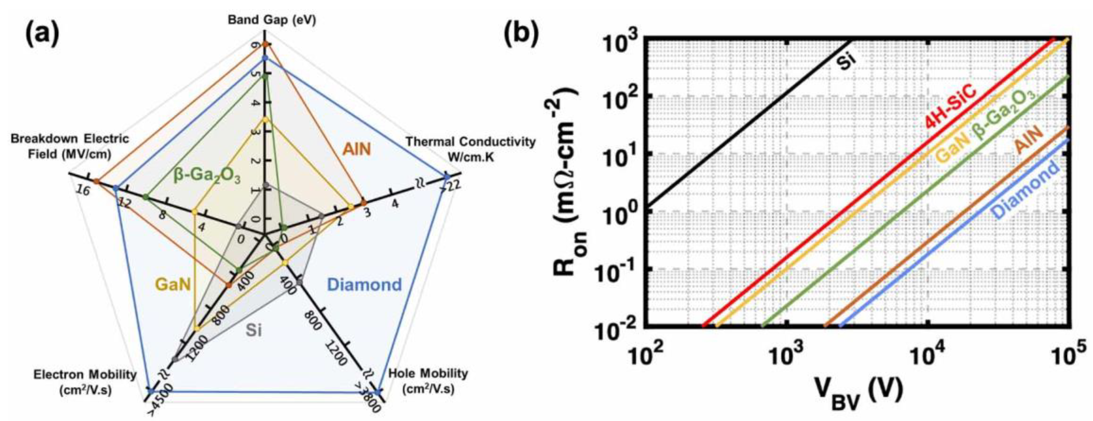
Figure 2.
Schematic diagram of a Molecular Beam Epitaxy (MBE) system. The system operates under ultra-high vacuum (UHV) conditions, utilizing effusion cells for atomic beam generation, a heated substrate for epitaxial growth, and RHEED for real-time monitoring of surface structure and growth rates [93].
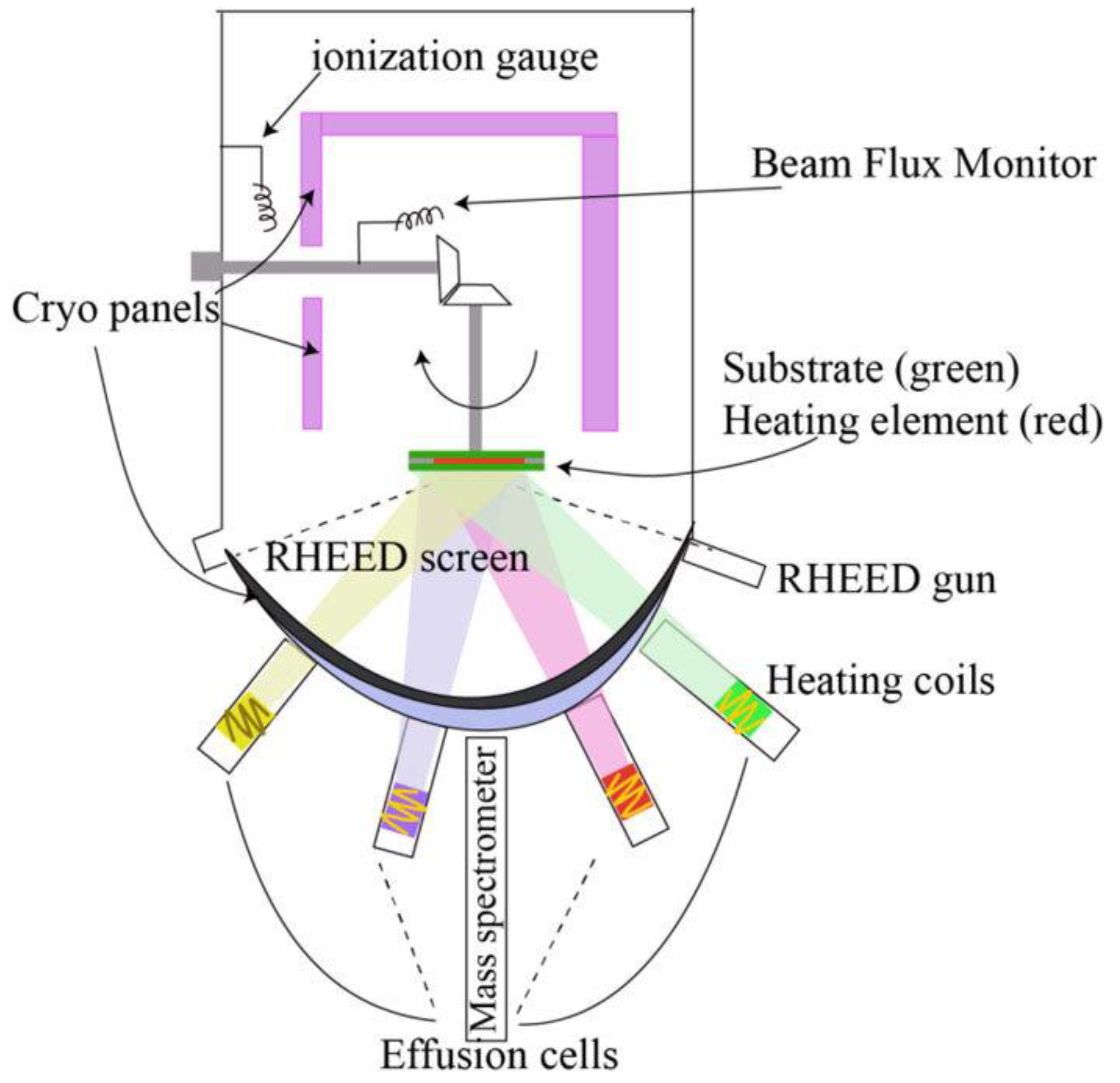
Figure 3.
Schematic diagrams of Chemical Vapor Deposition (CVD) systems. (a) Hot Filament CVD (HFCVD) system, where a heated filament decomposes precursor gases for uniform film deposition. (b) Plasma-Enhanced CVD (PECVD) system, utilizing plasma generated by a microwave source to enhance chemical reactions at lower substrate temperatures. Both systems enable the deposition of high-quality thin films for advanced material applications [101].
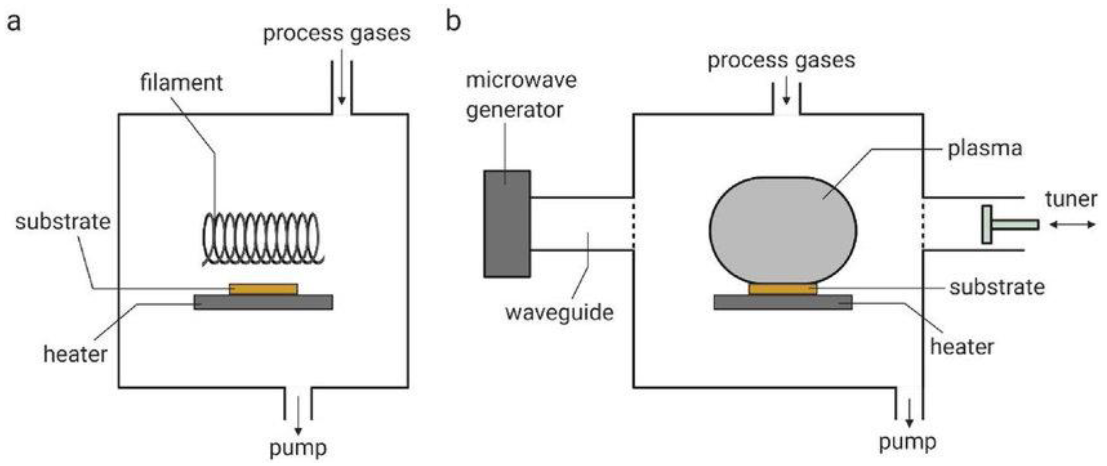
Figure 4.
Schematic diagram of a Metal-Organic Chemical Vapor Deposition (MOCVD) system. The system facilitates the deposition of Gallium Nitride (GaN) through chemical reactions between metal-organic precursors (e.g., trimethylgallium) and hydrides (e.g., ammonia) on a heated substrate. Key components include injectors for precursor delivery, a heated susceptor for the substrate, and an exhaust system for byproduct removal, all optimized to ensure uniform film growth and minimal impurities [114].
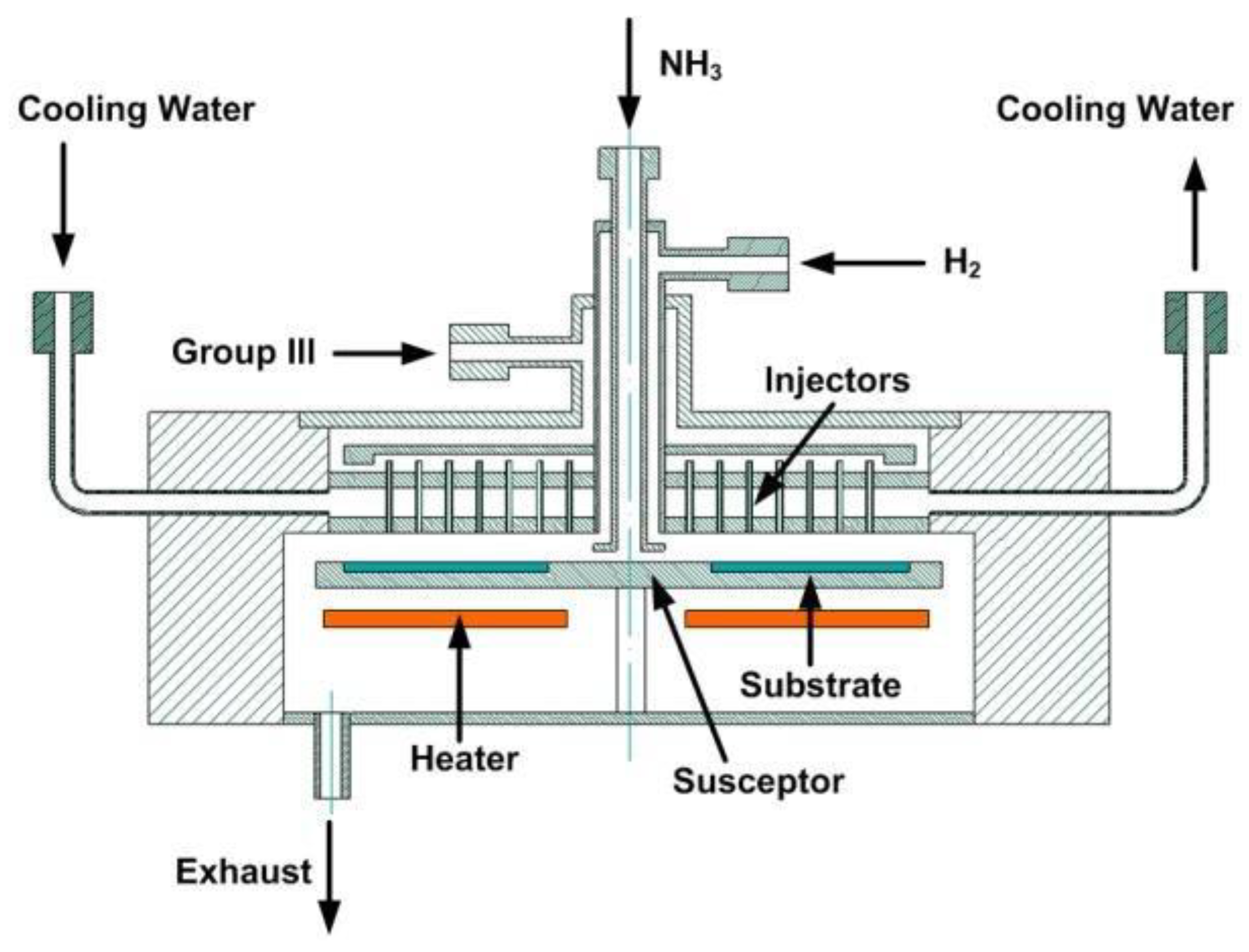
Figure 5.
Schematic diagram of a Hydride Vapor Phase Epitaxy (HVPE) system. GaN is synthesized via the reaction of gallium chloride (GaCl), formed from liquid gallium and hydrogen chloride (HCl), with ammonia (NH₃) in a high-temperature growth zone. The system features gas inlets for NH₃, HCl, and N₂, with distinct temperature zones (800–900°C and 1000–1100°C) to enable efficient and uniform GaN deposition [127].
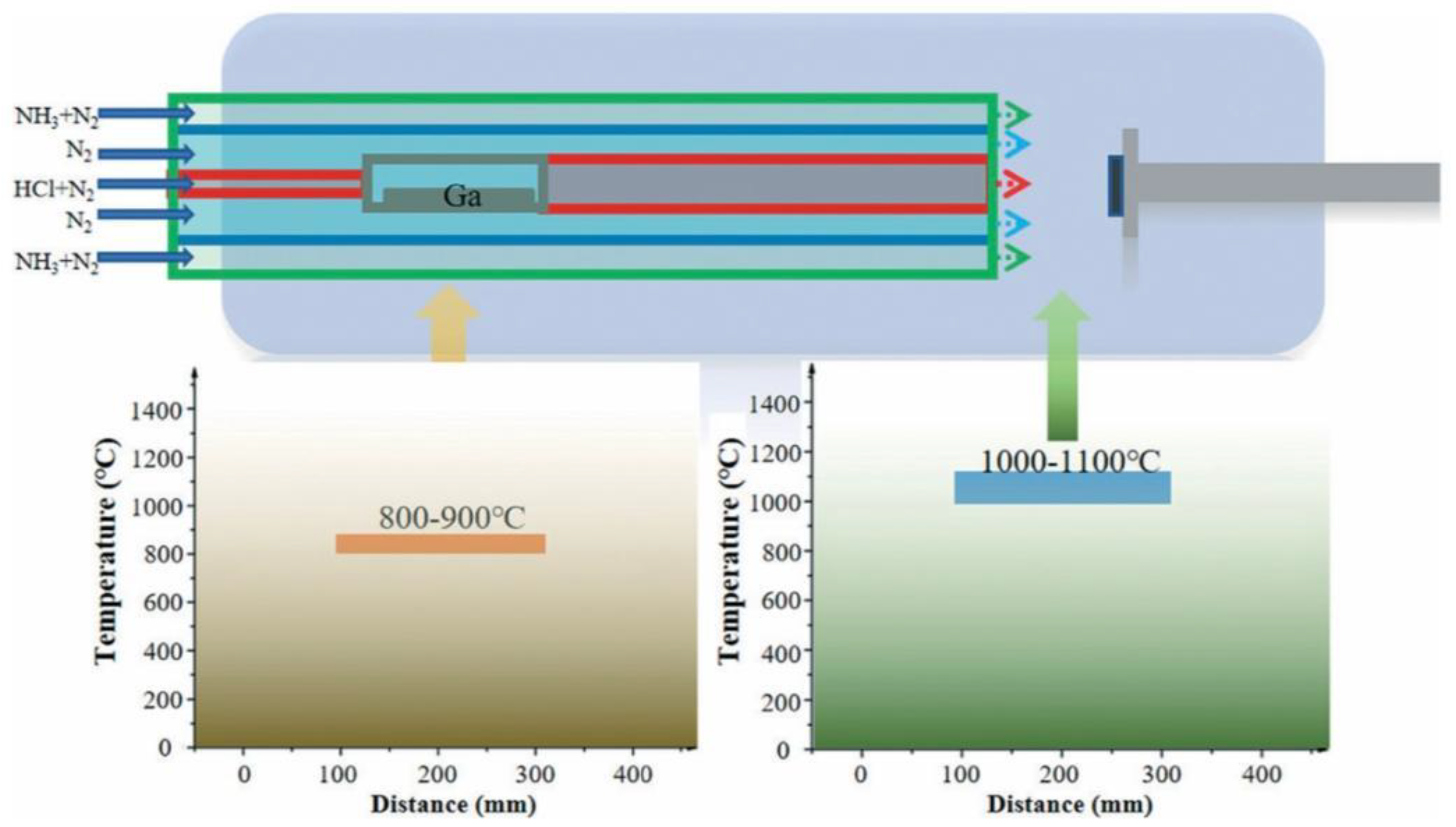
Figure 6.
Schematic diagram of a Liquid Phase Epitaxy (LPE) system. The process involves dipping a substrate into a molten growth solution contained in a platinum crucible, where an epitaxial layer forms as the temperature decreases. Key components include a Pt-wire substrate holder, a thermocouple for precise temperature control, a high-density ceramic furnace for heating, and alumina hardware for structural support. This setup ensures uniform epitaxial growth and high-quality layer formation critical for semiconductor applications [140].
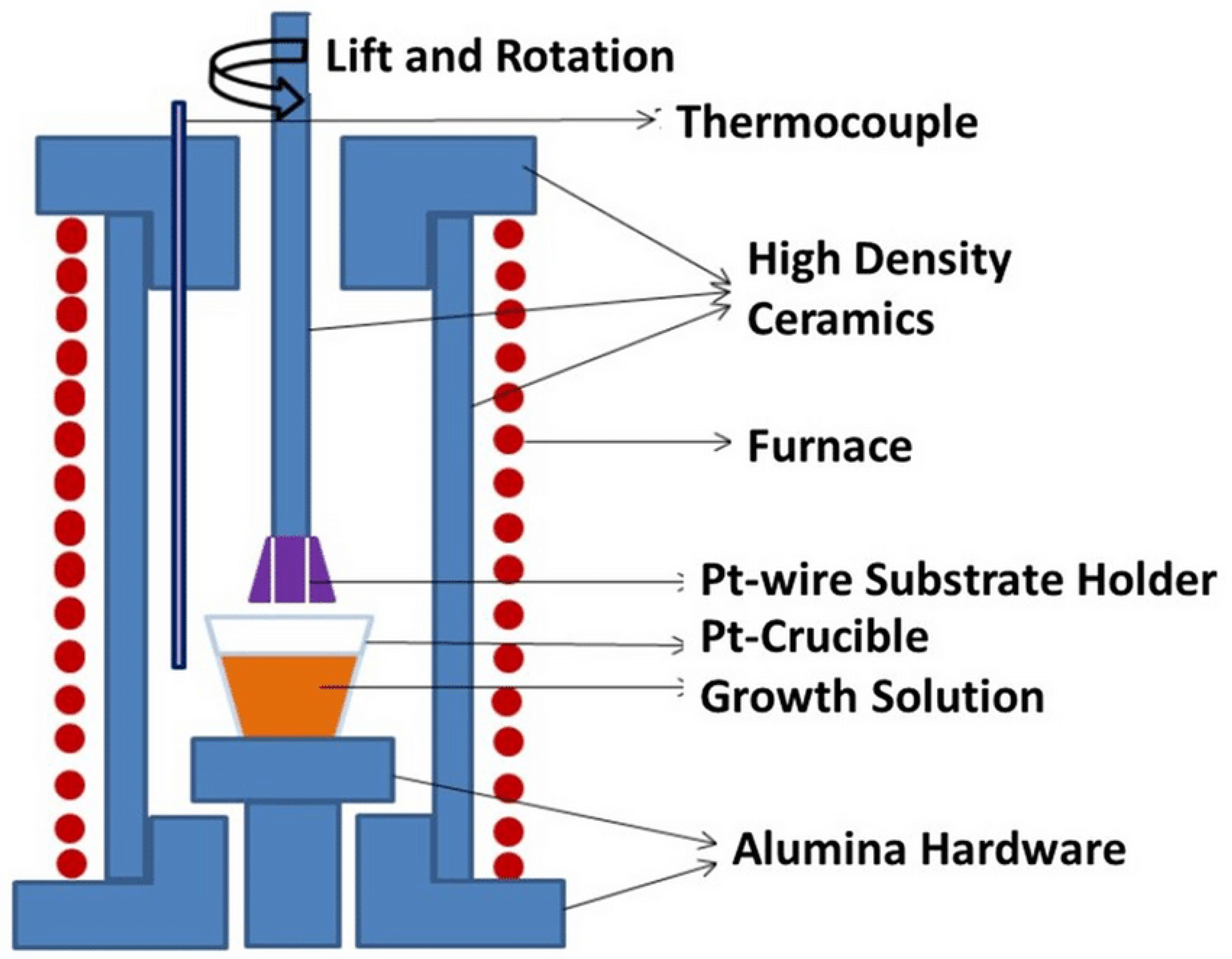
Figure 7.
Schematic diagram of the Atomic Layer Epitaxy (ALE) process. (a) A functionalized substrate is prepared; (b) Precursor A is introduced, forming a self-limiting monolayer; (c) Excess Precursor A and byproducts are purged; (d) Precursor B reacts with the monolayer; (e) Reaction byproducts are removed via purging; (f) The cycle is repeated to build the desired layer thickness with atomic precision [148].
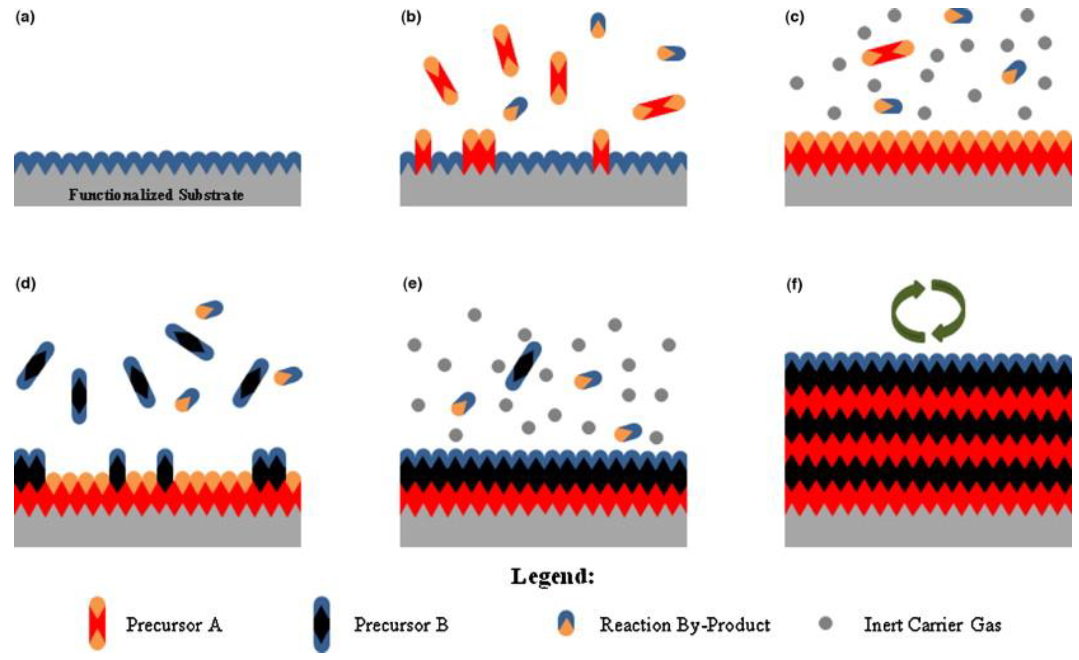
Figure 8.
Schematic of the Pulsed Laser Deposition (PLD) process, illustrating the key components and stages: a high-powered laser beam ablates the rotating target, forming a plasma plume that deposits material onto the heated substrate through a vacuum chamber [170].
Figure 8.
Schematic of the Pulsed Laser Deposition (PLD) process, illustrating the key components and stages: a high-powered laser beam ablates the rotating target, forming a plasma plume that deposits material onto the heated substrate through a vacuum chamber [170].
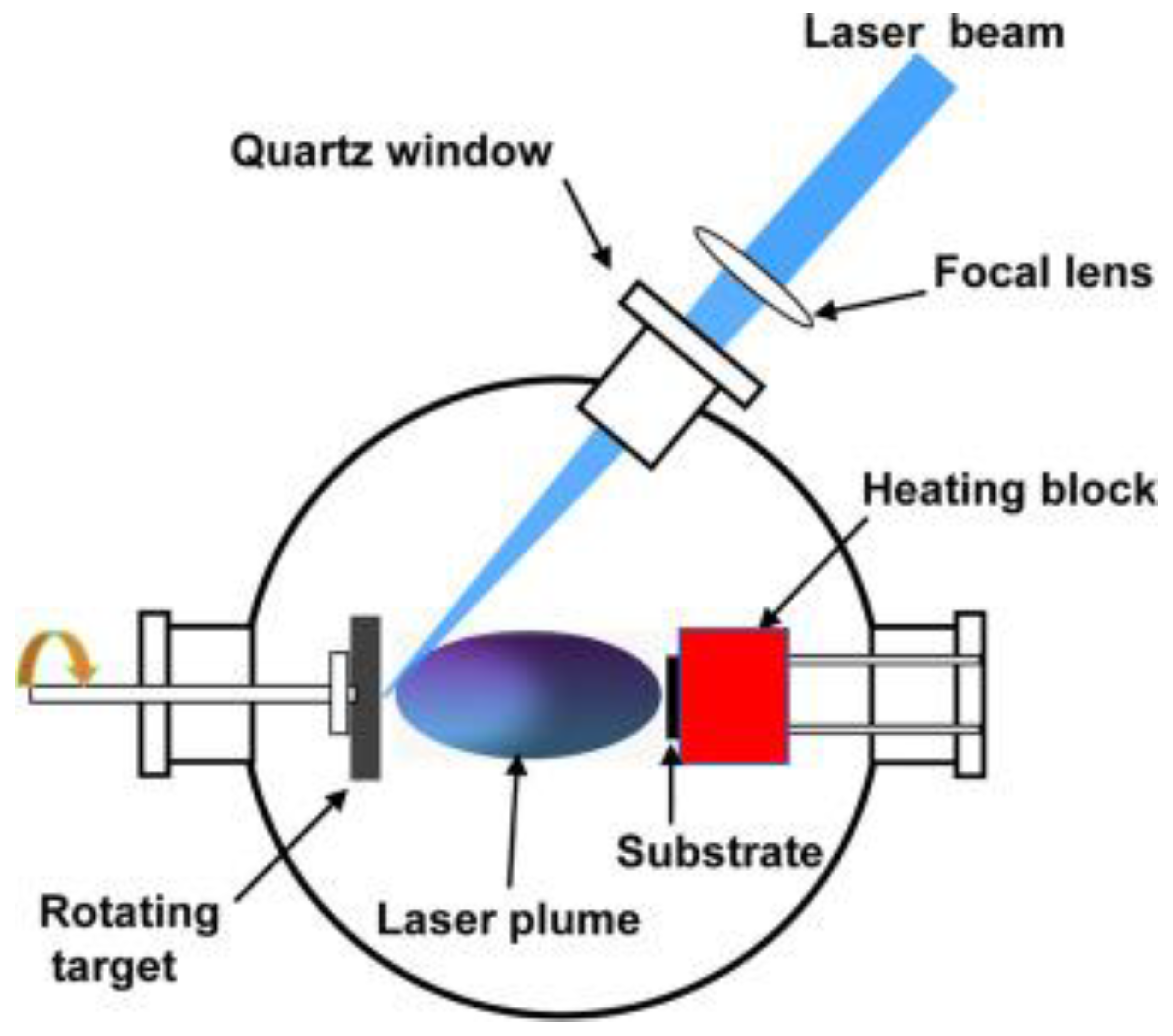

Table 1.
Properties of wide bandgap semiconductors [9].
Table 1.
Properties of wide bandgap semiconductors [9].
| Property | 4H-SiC | GaN | ZnO | In2o3 | IGZO | Ga2O3 | Diamond | AlN |
| Bandgap (eV) | 3.3 | 3.4 | 3.37 | 3.7 | 3.5 | 4.9 | 5.5 | 6.0 |
| Breakdown field (MV/cm) | 3.1 | 4.9 | 0.01 | NA | 2.7 | 10.3 | 4.4 | 15.4 |
| Sat. velocity (107cm/s) | 2.2 | 1.4 | 3.2 | 0.25 | 0.8 | 1.8 | 1.5 | 1.6 |
| Thermal conductivity (WmK-1) | 490 | 230 | 50 | 2.2 | 1.4 | 13 | 2200 | 320 |
| Johnson FOM ratio vs Si | 278 | 1089 | NA | NA | NA | 2844 | 81000 | 7744 |
| Baliga FOM ratio vs Si | 712 | 3170 | 10 | NA | 3.7 | 4125 | 62954 | 38181 |
| Tunneling eff. Mass (mo) | NA | 0.15 | 0.24 | 0.40 | 0.34 | 0.31 | 0.69 | NA |
| Melting point (oC) | 2730 | 2500 | 1975 | 1910 | 850 | 1700 | 3550 | 2830 |
| Thermal budget | High | High | Low | Low | Low | High | High | High |
| CMOS demonstration status | Cree 2006 | HRL 2016 | NA | NA | NA | NA | NA | NA |
Table 2.
Comparison of Different CVD Variants and Applications.
| Characteristic | Plasma-Enhanced CVD (PECVD) | Hot-filament CVD (HFCVD) | Low-Pressure CVD (LPCVD) | High-Temperature CVD (HTCVD) | Metal-Organic CVD (MOCVD) | Atmospheric Pressure CVD (APCVD) |
|---|---|---|---|---|---|---|
| Application | Diamond films | SiC layers | Si nanostructures | SiC for power electronics | Compound semiconductors | General coatings |
| Deposition Rate | Moderate to high | Moderate | High | Variable | Moderate | Variable |
| Deposition Temperature | Low (100 -300°C) | High (800 -1200°C) | Moderate to high (400 -800°C) | Very high (above 1200°C) | Moderate to high (300 - 700°C) | Ambient |
| Pressure | Low to atmospheric | Atmospheric | Low | High | Low to atmospheric | Atmospheric |
| Advantages | High quality, low temperature | Cost-effective, scalable | Uniformity, better control | High-quality crystals | Precise composition control | Simplicity and low cost |
| Disadvantages | Equipment complexity | High temperature requirements | Longer deposition times | Energy-intensive | Toxic precursor materials | Limited control over thickness |
| Cost | Moderate to high | Moderate | Moderate | High | High | Low |
| Film Quality | Excellent uniformity | Good crystalline quality | High uniformity and purity | Exceptional crystal quality | Excellent film properties | Variable quality |
Table 3.
Growth Rates and Defect Density Achieved by GaN and AlGaN with MOCVD.
| Material | Growth Rate (μm/h) | Defect Density (cm-2) |
|---|---|---|
| GaN | 1 – 3 | 106 - 108 |
| AlGaN | 0.5 – 2 | 106 - 109 |
Table 4.
Characteristics of Materials Grown by LPE.
| Material | Growth Rate (μm/h) | Application |
|---|---|---|
| GaAs | 5 – 10 | LEDs, solar Cells |
| InP | 1 – 5 | High-Speed electronics |
Table 5.
Key Parameters in Pulsed Laser Deposition.
| Parameter | Value or Range | Effect on Growth |
|---|---|---|
| Laser Fluence | 1J/cm2 to 10J/cm2 | Controls ablation efficiency and film quality |
| Substrate Temperature | 300 – 800oC | Affects crystallinity and morphology |
| Oxygen Pressure (for oxides) | 10-6 Torr to 10-2 Torr | Determines stoichiometry in oxide films |
Table 6.
Comparative Overview of Epitaxial Growth Techniques.
| Technique | Key Characteristics | Applications | Advantages | Challenges | Scalability | Cost | Uniformity |
| Molecular Beam Epitaxy (MBE) | Utilizes molecular beams in ultra-high vacuum; precise atomic layer control | Quantum wells, superlattices, GaN, SiC, AlGaN | Atomic precision, low contamination, ideal for heterostructures | Slow growth rates, high cost, limited scalability | Limited Scalability | High | Excellent |
| Metal-Organic Chemical Vapor Deposition (MOCVD) | Gas-phase chemical reactions; uses metal-organic precursors | LEDs, laser diodes, solar cells, power devices | High throughput, scalable, versatile for complex structures | High defect density, uniformity issues, toxic precursors | Highly scalable | Moderate | Moderate |
| Hydride Vapor Phase Epitaxy (HVPE) | Involves gas-phase reactions with hydrides; effective for thick layers | Bulk GaN substrates, high-power electronics | High growth rate, suitable for large-area substrates | High defect density, substrate bowing, lattice mismatch | Scalable for thick layers | Moderate | Moderate |
| Chemical Vapor Deposition (CVD) | Vapor-phase chemical reactions; various types like PECVD and HFCVD | Diamond, SiC, solar cells | Precise control, scalable, applicable to 2D and polymeric films | High precursor cost, temperature-sensitive, uniformity challenges | Highly scalable | Moderate | Variable |
| Liquid Phase Epitaxy (LPE) | Deposition from molten solution, typically high temperature | LEDs, laser diodes, photovoltaic cells | Cost-effective, suitable for thick layers, high purity | Difficult to achieve ultrathin layers, lacks precise layer control | Limited scalability | Low | Moderate |
| Atomic Layer Epitaxy (ALE) | Sequential, self-limiting reactions enable atomic layer precision | Transistors, sensors, quantum wells | Atomic-scale precision, uniformity, ideal for nanostructures | Slow growth rate, complex control, high cost | Limited scalability | High | Excellent |
| Pulsed Laser Deposition (PLD) | High-energy laser ablation of target material, allowing for diverse thin-film compositions | Complex oxides, solar cells, superconductors | High crystalline quality, flexibility in compositions and structures | Requires high energy, scalability issues, film quality variations | Limited scalability | Moderate | Variable |
Disclaimer/Publisher’s Note: The statements, opinions and data contained in all publications are solely those of the individual author(s) and contributor(s) and not of MDPI and/or the editor(s). MDPI and/or the editor(s) disclaim responsibility for any injury to people or property resulting from any ideas, methods, instructions or products referred to in the content. |
© 2024 by the authors. Licensee MDPI, Basel, Switzerland. This article is an open access article distributed under the terms and conditions of the Creative Commons Attribution (CC BY) license (http://creativecommons.org/licenses/by/4.0/).
Copyright: This open access article is published under a Creative Commons CC BY 4.0 license, which permit the free download, distribution, and reuse, provided that the author and preprint are cited in any reuse.


