
Submitted:
12 April 2025
Posted:
14 April 2025
You are already at the latest version
Abstract
This study explores advancements in photovoltaic technologies by enhancing the optoelectronic properties and electronic quality of multicrystalline Silicon (mc-Si) through silicon nitride (SiNx) and hydrogen (H2) plasma deposition via Plasma-Enhanced Chemical Vapor Deposition (PECVD). This innovative approach replaces toxic chemical wet processes with H2 plasma and SiNx, promoting environmentally friendly and sustainable energy solutions. Key parameters of silicon solar cells, including effective lifetime (τeff), diffusion length (Ldiff), in addition to the iron concentration ([Fe]), were analyzed before and after this sustainable solution. The results show significant improvements, particularly in the edge region, which initially exhibited low τeff and a high iron concentration. After treatment, τeff and Ldiff increased to 7 μs and 210 μm, respectively, compared to 2 μs and 70 μm for untreated mc-Si. Additionally, the [Fe] decreased significantly after the process, dropping from 60 ppt to 10 ppt in most regions. Furthermore, the treatment led to a significant decrease in reflectivity, from 25% to 8% at a wavelength of 500 nm. These findings highlight the effectiveness of PECVD-SiNx and H2 plasma treatments in improving the optoelectronic performance of mc-Si, making them promising for high-efficiency photovoltaic devices.
Keywords:
multicrystalline Silicon
; PECVD-SiNx
; PV technologies
; sustainable
; effective lifetime
; diffusion length
; iron concentration
1. Introduction
One of the significant advances in photovoltaic (PV) technology is the development of high-efficiency solar cells [1,2,3,4]. Innovations in cells design and manufacturing processes have led to substantial improvements in conversion efficiency, enhancing both performance and sustainability in solar energy production [5,6]. However, challenges such as defects and impurities in silicon and more specifically in mc-Si remain significant barriers to improving its electronic quality [7,8,9]. These defects reduce considerably solar cell efficiency by increasing charge carrier recombination [10,11], thereby limiting overall energy output. Additionally, traditional manufacturing processes often rely on hazardous and toxic chemicals, posing risks to both human health and the environment [12]. To overcome these challenges, advanced photovoltaic technologies are being developed to enhance mc-Si electronic quality and eliminate the use of toxic chemicals. Innovations such as PECVD, gettering techniques, and defect passivation [13,14,15] help reduce impurities leading to high efficiency. Furthermore, sustainable and non-toxic manufacturing methods are being explored to minimize environmental impact [16]. These advancements are crucial for the future of sustainable energy, ensuring that silicon-based solar PV technology remains both efficient and environmentally friendly, which leads to clean energy solutions. Advanced photovoltaic technologies aim to enhance the optical, electrical, and optoelectronic properties of multicrystalline silicon wafers through a combination of surface treatments and bulk purification [17,18]. It is important to note that reducing the surface recombination velocity of minority carriers and optical losses significantly impacts solar cells' efficiency. Moreover, the grain boundaries (GBs) lead to a potential barrier for charge carriers and thereby affect the majority carrier mobility as reported by Maruska et al. [19]. Metallic impurities, particularly transition metals (Fe, Cu, etc.), are typically present in mc-Si with high concentrations. These impurities act as charge carrier trapping centers, leading to dramatic degradation of the photovoltaic performance of mc-Si-based solar cells. Surface treatment and gettering of undesirable impurities are widely used techniques to enhance the optical, electrical, and optoelectronic properties of multicrystalline silicon. Surface treatment reduces surface recombination by passivating defects and minimizing optical losses, improving charge carrier lifetime and overall efficiency. Meanwhile, gettering processes, such as extrinsic gettering using silicon nitride and hydrogen plasma, effectively remove metallic impurities like Fe, Cu, Ni, and Cr. These impurities act as recombination centers, degrading the photovoltaic performance of mc-Si-based solar cells. By combining surface passivation and impurities removal, these techniques significantly improve charge carrier mobility, diffusion length, and overall optoelectronic quality, making mc-Si more suitable for high-efficiency solar cell applications. This study examines the gettering effect of impurities present in the bulk of the multicrystalline silicon substrates, which have been grooved, and treated with porous silicon (PS), followed by Rapid Thermal Processing (RTP). PS serves as a sacrificial layer to trap impurities after their diffusion. Following the removal of the PS layer, plasma-enhanced chemical vapor deposition is employed to deposit silicon nitride and hydrogen plasma onto the mc-Si substrate.
2. Materials and Methods
2.1. Samples Preparation for the PECVD Process
The experimental process is described in Figure 1. The substrate used in this experimental process is p-type mc-Si with a thickness of 450 µm, dimensions of 10 × 10 cm², and a resistivity ranging from 0.5 to 2.0 Ω·cm. The sample preparation involved a combination of grain boundary (GBs) etching and the formation of porous silicon. The samples underwent the following sequential treatments: First, the GBs were grooved by immersing the samples in a mixture solution of (HF (48%): HNO3 (65%)) with a volume ratio of (4:1) during 10s followed by rinsing in deionized water and drying under N2 flow (see Figure 2a) PS layers were formed on both sides of the wafers using the Stain etching method [20] which consists of dipping samples in an aqueous (HF (40%): HNO3 (65%): H2O) solution with a (1:3:5) volume ratio during 120s (see Figure 2b). PS formations was followed by a rapid thermal treatment in an infrared furnace under an argon atmosphere for 1 hour at 850°C. The purpose of this thermal treatment is to concentrate unwanted impurities in the inactive region of PS layers on both sides of the substrates. To eliminate the trapped impurities, the porous silicon layer was removed following a two-step process. the first step was to eliminate the silicon oxide (SiO2) layer formed after annealing using a diluted HF solution (10%), then the PS layer is removed using aqueous sodium hydroxide (NaOH) solution (1M) to obtain a treated mc-Si, referred as T-mc-Si.
2.2. PECVD Application
The prepared samples underwent the plasma-enhanced chemical vapor deposition treatment to deposit silicon nitride and hydrogen plasma. To examine the passivation characteristics of PECVD-deposited SiNx, hydrogen plasma pre-treatment was employed, substituting the conventional toxic wet chemical cleaning. This in-situ process, conducted within the PECVD reactor before SiNx deposition, eliminated the need for hazardous chemicals and maintained a continuous vacuum environment [21] in addition to silicon antireflective properties enhancement. It is important to note that the damage caused by hydrogen plasma can be eliminated through annealing at temperatures above 600°C, at which point hydrogen can diffuse outward, promoting bulk passivation. For PECVD deposition of SiNx [21], the reactive gases used are SiH₄ and NH₃, with N₂ as a carrier or diluting gas [22]. The SiH₄/NH₃ gas ratio controls SiNx film stoichiometry (stoichiometric, Si-rich, or N-rich). RF power adjusts film stress via surface bombardment, higher power yields compressive stress. Conversely, increased pressure increases tensile stress and reduces film density. Table 1 summarizes the optimized parameters for the SiN layer deposition and hydrogen plasma treatment.
2.3. Characterization Tools
The cross-section and surface structure of the samples were measured with a scanning electron microscope (SEM, JEOL JSM-5400). A FT-IR spectrometer (Nicolet MAGNA-IR 560 ESP FT-IR) was used to examine the elemental analysis of the treated mc-Si. Reflectivity spectra were obtained using a UV/Vis/NIR Spectrophotometer (Perkin-Elmer Lambda 950) with an integrating sphere. Finally, using a Semilab WT-2000PVN Multifunction Wafer Mapping Tool, high-resolution maps of carrier lifetime, diffusion length, and iron concentration were generated. The tool's 904 nm laser enabled approximately 30 µm deep excitation of the silicon.
3. Results and Discussion
The SiNx: H spectrum demonstrated in Figure 3 consists of typical absorption bands for different N-H bonds and bands related to Si-N, Si-O, and Si-H bonds [23]. The spectrum shows two absorption peaks at 460 cm⁻¹ and around 850-879 cm⁻¹, which are associated with the vibration mode of the Si-N. Additionally, there are two absorption peaks related to the vibration mode of the N-H bond at 1150 cm⁻¹ and 3342 cm⁻¹. Furthermore, the absorption peaks associated with the vibration modes of Si-O and Si-H are located at 1073 cm⁻¹ and around 2200-2250 cm⁻¹, respectively. The final absorption peak is located at 3320 cm⁻², corresponding to the vibration of N-Si-H. After hydrogen plasma treatment, it can be observed that the N-H bonds disappear, and Si-O bonds appear at 1080 cm⁻¹, indicating the onset of some oxidation. Silicon oxynitride (SiOxNy), being a tetrahedral amorphous alloy, shows peaks corresponding to Si-O and Si-N bonds, indicating the formation of a SiOxNy layer [24,25,26]. The shift in the maxima of the absorption peaks corresponding to Si-O and Si-N bonds depends on the substitution of nitrogen atoms for oxygen atoms during plasma treatment. It is well known that the Si-H content is crucial for passivation quality.
Scanning Electron Microscopy (SEM) was used to characterize the surface morphology of mc-Si samples following these treatments. As shown in Figure 4, the H2/SiNx surface treatment significantly increases the effective area that interacts with incoming light compared to the reference sample. This treatment plays a crucial role in improving light absorption in solar cells by inducing multiple internal reflections within mc-Si. The rough surface scatters incoming light instead of reflecting it away, promoting diffused reflection and reducing reflection losses
Figure 5 shows the total reflectance of the mc-Si sample after different treatments, Figure 5a for Bare mc-Si, Figure 5b for PS-treated groove mc-Si, and Figure 5c for PS-treated groove mc-Si with SiNx/hydrogen plasma in the wavelength range of 300-1200 nm. It can be observed that a significant reduction in reflectivity occurs for the sample that underwent a combination of PS-treated groove mc-Si in the entire wavelength range compared to untreated one, where the reflectivity decreases from 25% to 14% at the wavelength of 500 nm. This reduction in the reflectivity is linked to the etching of the grain boundaries (GBs) and the change in the grain surface. Indeed, the V-shape of the GBs obtained after etching allows at least double the reflection of the light beam that reaches the GBs. The results also show that the SiNx/hydrogen plasma layer can reduce reflectivity to 8% at 500 nm. This reflection increases the number of photons absorbed by the mc-Si substrate, thereby increasing the photocurrent. Moreover, the reduction in reflectivity after the SiNx/hydrogen plasma layer formation is attributed to the intermediate step of the H₂ plasma, which leads to the formation of a double-layer antireflective coating with SiNx and the formation of nanostructures mc-Si surface (see Figure 4c).
To evaluate the electronic quality of mc-Si substrates treated with H₂ plasma and SiNx by the PECVD technique, 2D mappings of τeff, Ldiff, and [Fe] were performed before and after each treatment. The resulting maps are shown in Figure 6. It is observed that after SiNx and plasma H2, the distribution of τeff, Ldiff, and [Fe] showed significant changes compared to the bare mc-Si. The main observation is the complete transformation in the edge region, which initially exhibited low τeff values and very high [Fe]. Consequently, after treatment, the most significant improvements in τeff, Ldiff, and [Fe] were obtained in the edge region. The mappings of τeff and Ldiff showed an increase, with τeff and Ldiff reaching 7 µs and 210 µm, respectively (Figure 6b), compared to the bare mc-Si, where the average values of τeff and Ldiff are approximately 3 µs and 105 µm (Figure 6a). Furthermore, the change in the [Fe] distribution after treatment was also more significant, with the concentration decreasing in most areas of the wafer, from 52 ppt to reaching minimum values of 10 ppt. A correlation between the reduction of [Fe] and the augmentation of τeff and Ldiff was observed in the totality of the mc-Si surface, signifying substantial impurity passivation mediated by SiNx and H₂ plasma. The implemented gettering protocol exhibited high efficacy, yielding satisfactory values for τeff, Ldiff, and [Fe].
Another critical phenomenon examined in this study is the impact of T-mc-Si on the edge regions of mc-Si wafers. As shown in Figure 7, the carrier lifetime mapping of a mc-Si wafer (10 cm × 10 cm), measured using the µ-PCD technique, indicates that the wafers were extracted from the edge of the mc-Si ingot, where the effective minority carrier lifetime (τeff) exhibits a pronounced reduction, particularly along the left and lower edges. Figure 8 shows that the region with very low τeff (~ 1 µs) extends approximately 0–15 mm from the wafer edge and gradually increases between 15 and 100 mm.
Jiang et al. [16] demonstrated that the low eff of minority carriers in the edge region of Si-mc ingots negatively impacts the electronic quality of wafers. They found no direct correlation between this low τeff and the concentrations of substitutional carbon, interstitial oxygen, or dislocations density. However, iron contamination was identified as the primary cause of eff degradation in the edge region of mc-Si. In this section, we analyze the correlation between iron concentration and eff in mc-Si wafers, considering the effect of T-mc-Si. The iron concentration in the reference wafer reaches 1×10¹³ cm⁻³ at the edges and gradually decreases to 3.2 × 10¹² cm⁻³ at the center. This confirms the eff distribution and highlights the detrimental effect of iron (see Figure 8). The progressive increase in interstitial iron contamination toward the edges may be attributed to iron incorporation during directional solidification [27]. After T-mc-Si, [Fe] significantly decreases to 2.6 × 10¹² cm⁻³, demonstrating the effectiveness of the treatment in reducing contamination. The same phenomenon was observed for Ldiff distribution mapping on Si-mc. For a reference sample, Ldiff values range from 59 µm to 105 µm, with the lowest values at the edges. After T-mc-Si, Ldiff improves significantly, ranging from 69 µm to 118 µm, with a notable increase at the edges.
5. Conclusions
In summary, an innovative approach through hydrogen plasma and silicon nitride was used in this investigation via the PECVD technique, which reveals a significant improvement in the optical and optoelectronic properties of mc-Si. As a result, the optoelectronic parameters such as τeff and Ldiff show substantial enhancement, where τeff and Ldiff reach 7 µs and 210 µm, respectively, compared to the bare mc-Si, where the values of τeff and Ldiff are approximately 2 µs and 70 µm. Furthermore, the change in [Fe] after gettering is also more significant, with the concentration decrease in most areas of the wafer, reaching minimum values of 10 ppt. The reflectivity shows a significant reduction from 25 % to about 8% for the wafer that underwent a combination of T-mc-Si and H2 plasma/SiNx at the wavelength of 500 nm, compared to the reference sample. The experimental results suggest that the obtained sample has spectacular passivation and high electronic quality of the mc-Si surface.
Author Contributions
All authors contributed to the study's conception and design. Conceptualization, M.B.R and A.E.H.; methodology, A.M. and R.B.Z; software, K.C.; validation, M.A.A., W.D. and M.B.R.; formal analysis, A.E.H.; investigation, A.M and R.B.Z; resources, K.C.; data curation, M.A.A.; writing—original draft preparation, W.D.; writing—review and editing, M.B.R.; visualization, K.C.; supervision, M.B.R.; project administration, K.C.; funding acquisition, K.C. All authors have read and agreed to the published version of the manuscript.
Funding
This work was supported and funded by the Deanship of Scientific Research at Imam Mohammad Ibn Saud Islamic University (IMSIU) (grant number IMSIU-DDRSP2502.
Data Availability Statement
The datasets generated during and/or analyzed during the current study are available from the corresponding author upon reasonable request.
Conflicts of Interest
The authors declare no conflicts of interest.
References
- Ogundipe, O. B.; Okwandu, A. C.; Abdulwaheed, S. A. Recent advances in solar photovoltaic technologies: Efficiency, materials, and applications. GSC Advanced Research and Reviews 2024, 20(1), 159–175. [Google Scholar] [CrossRef]
- Vodapally, S. N.; Ali, M. H. A comprehensive review of solar photovoltaic (PV) technologies, architecture, and its applications to improved efficiency. Energies 2022, 16(1), 319. [Google Scholar] [CrossRef]
- Yamaguchi, M.; Masuda, T.; Araki, K.; Sato, D.; Lee, K. H.; Kojima, N.; Yamazaki, M. Development of high-efficiency and low-cost solar cells for PV-powered vehicles application. Progress in Photovoltaics: Research and Applications 2021, 29(7), 684-693.
- Yamaguchi, M.; Dimroth, F.; Geisz, J. F.; Ekins-Daukes, N. J. Multi-junction solar cells paving the way for super high-efficiency. Journal of Applied Physics 2021, 129(24). [CrossRef]
- Green, M. A.; & Bremner, S. P. Energy conversion approaches and materials for high-efficiency photovoltaics. Nature materials 2017, 16(1), 23–34. [Google Scholar] [CrossRef] [PubMed]
- Ashraf, M.; Ayaz, M., Khan; M., Adil, S. F.; Farooq, W.; Ullah, N.; Nawaz Tahir, M. Recent trends in sustainable solar energy conversion technologies: mechanisms, prospects, and challenges. Energy & Fuels 2023, 37(9), 6283-6301. [CrossRef]
- Yu, W.; Xue, Y.; Mei, J.; Zhou, X.; Xiong, M.; Zhang, S. Segregation and removal of transition metal impurities during the directional solidification refining of silicon with Al-Si solvent. Journal of Alloys and Compounds 2019, 805, 198–204. [Google Scholar] [CrossRef]
- Lv, X.; Li, H.; Ding, D.; Yu, X.; Jin, C.; Yang, D. Interfacial characterization of non-metal precipitates at grain boundaries in cast multicrystalline silicon crystals. Journal of Crystal Growth 2025, 652, 128042. [Google Scholar] [CrossRef]
- Wang, L.; Liu, J.; Li, Y.; Wei, G.; Li, Q.; Fan, Z.; He, D. Dislocations in Crystalline Silicon Solar Cells. Advanced Energy and Sustainability Research 2024, 5(2), 2300240. [Google Scholar] [CrossRef]
- Yoon, Y.; Yang, W. C. D.; Ha, D.; Haney, P. M.; Hirsch, D.; Yoon, H. P.; Zhitenev, N.B. Unveiling defect-mediated charge-carrier recombination at the nanometer scale in polycrystalline solar cells. ACS applied materials & interfaces 2019, 11(50), 47037-47046. [CrossRef]
- Dasilva-Villanueva, N.; Catalán-Gómez, S.; Marrón, D. F.; Torres, J. J.; García-Corpas, M.; del Cañizo, C. Reduction of trapping and recombination in upgraded metallurgical grade silicon: impact of phosphorous diffusion gettering. Solar Energy Materials and Solar Cells 2022, 234, 111410. [Google Scholar] [CrossRef]
- Kwak, J. I.; Nam, S. H.; Kim, L.; An, Y. J. Potential environmental risk of solar cells: Current knowledge and future challenges. Journal of Hazardous Materials 2020, 392, 122297. [Google Scholar] [CrossRef] [PubMed]
- Achref, M.; Khezami, L.; Mokraoui, S.; Rabha, M. B. Effective surface passivation on multi-crystalline silicon using aluminum/porous silicon nanostructures. Surfaces and Interfaces 2020, 18, 100391. [Google Scholar] [CrossRef]
- Rabha, M. B.; Salem, M.; El Khakani, M. A.; Bessais, B.; Gaidi, M. Monocrystalline silicon surface passivation by Al2O3/porous silicon combined treatment. Materials Science and Engineering: B 2013, 178(9), 695-697. [CrossRef]
- Khezami, L.; Jemai, A. B.; Alhathlool, R.; Rabha, M. B. Electronic quality improvement of crystalline silicon by stain etching-based PS nanostructures for solar cells application. Solar Energy 2016, 129, 38–44. [Google Scholar] [CrossRef]
- Ullah, N.; Ahmad, A.; Sarfaraz, R.; Khalid, S.; Ali, I.; Younas, M.; Rezakazemi, M. Challenges and solutions in solar photovoltaic technology life cycle. ChemBioEng Reviews 2023, 10(4), 541–584. [Google Scholar] [CrossRef]
- Alrasheedi, N. H. The effects of porous silicon and silicon nitride treatments on the electronic qualities of multicrystalline silicon for solar cell applications. Silicon 2024, 16(4), 1765–1773. [Google Scholar] [CrossRef]
- Almeshaal, M. A.; Abdouli, B.; Choubani, K.; Khezami, L.; Rabha, M. B. Study of porous silicon layer effect in optoelectronics properties of multi-crystalline silicon for photovoltaic applications. Silicon 2023, 15(14), 6025–6032. [Google Scholar] [CrossRef]
- Maruska, H.P.; Ghosh, A.K.; Rose, A.; Feng, T. Hall mobility of polycrystalline silicon, Appl. Phys. Lett 1980. 36 (5) 381. [CrossRef]
- Raji, M.; Gurusamy, A.; Manikkam, S.; Perumalsamy, R. Monocrystalline Silicon Wafer Recovery Via Chemical Etching from End-of-Life Silicon Solar Panels for Solar Cell Application. Silicon 2024, 16(9), 3669–3688. [Google Scholar] [CrossRef]
- Yousuf, H.; Khokhar, M. Q.; Rahman, R.; Mengmeng, C.; Aida, M. N.; Madara, P. C.; Yi, J. Enhanced field-assisted passivation and optical properties improvement of PECVD deposited SiNx: H thin film. Optical Materials 2025, 162, 116885. [Google Scholar] [CrossRef]
- Fukata, N.; Sasaki, S.; Murakami, K.; Ishioka, K.; Nakamura, K. G.; Kitajima, M.; Haneda, H. Hydrogen molecules and hydrogen-related defects in crystalline silicon. Physical Review B 1997, 56(11), 6642. [Google Scholar] [CrossRef]
- Lelièvre, J. F.; Fourmond, E.; Kaminski, A.; Palais, O.; Ballutaud, D.; Lemiti, M. Study of the composition of hydrogenated silicon nitride SiNx: H for efficient surface and bulk passivation of silicon. Solar Energy Materials and Solar Cells 2009, 93(8), 1281–1289. [Google Scholar] [CrossRef]
- Rebib, F., Tomasella, E., Bêche, E., Cellier, J., Jacquet, M. FTIR and XPS investigations of a-SiOxNy thin films structure. In Journal of Physics: Conference Series 2008, 100, No. 8, p. 082034. IOP Publishing. [CrossRef]
- Mohamed, H. FTIR and Spectroscopic Ellipsometry Investigations of the Electron Beam Evaporated Silicon Oxynitride Thin Films. Physica B 2011, 406, 211–215. [Google Scholar] [CrossRef]
- Ghosh, H.; Mitra, S.; Saha, H.; Datta, S. K.; Banerjee, C. Argon plasma treatment of silicon nitride (SiN) for improved antireflection coating on c-Si solar cells. Materials Science and Engineering: B 2017, 215, 29–36. [Google Scholar] [CrossRef]
- Macdonald, D.; Cuevas, A.; Kinomura, A.; Nakano, Y.; Geerligs, L. J. Transition-metal profiles in a multicrystalline silicon ingot. Journal of Applied Physics 2005, 97(3). [CrossRef]
Figure 1.
Experimental process.
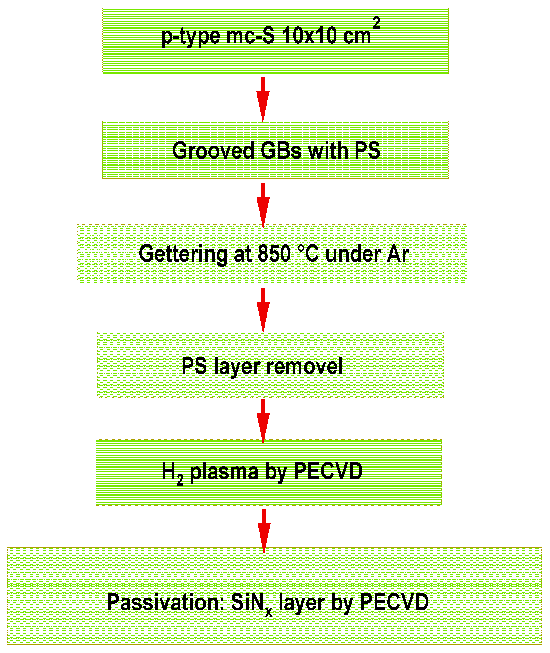
Figure 2.
SEM images of mc-Si after grain boundary (GB) grooving (a) with and (b) without PS treatment.
Figure 2.
SEM images of mc-Si after grain boundary (GB) grooving (a) with and (b) without PS treatment.
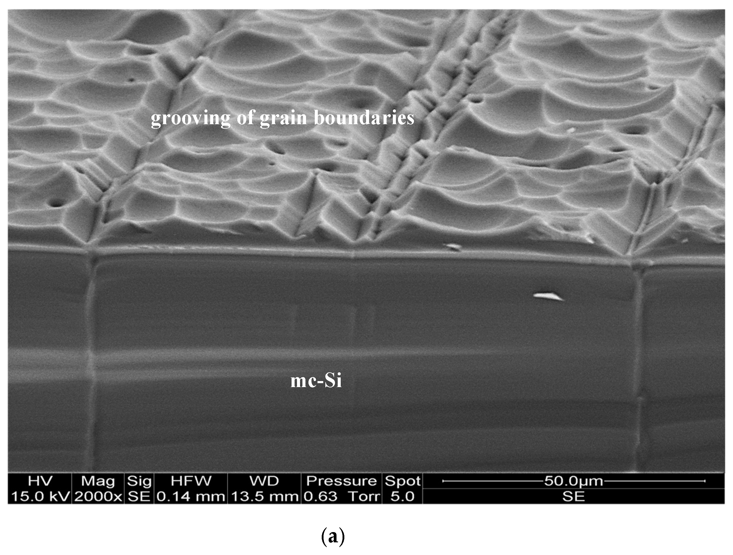
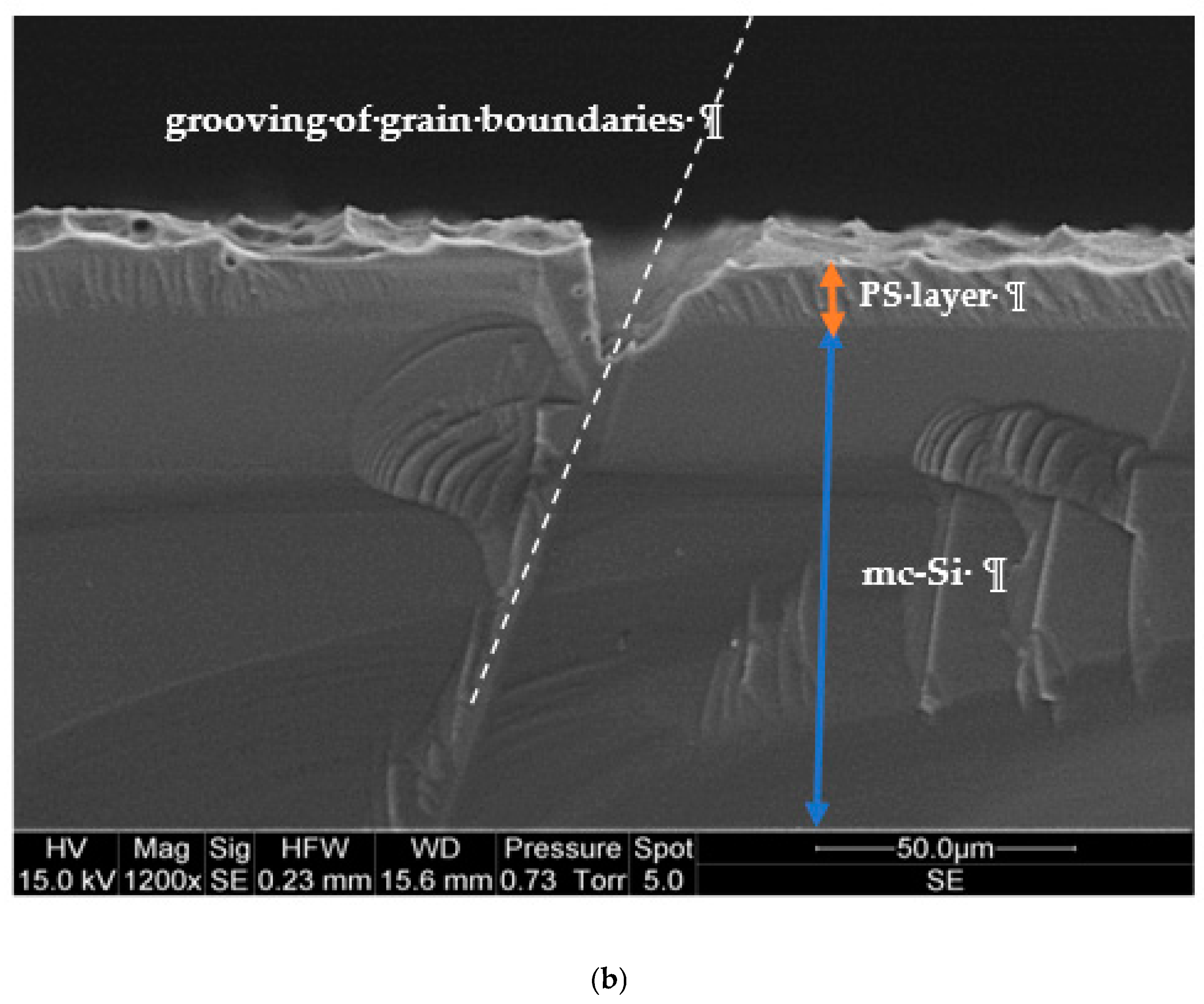
Figure 3.
FTIR Spectrum of (a) SiNx layer and (b) H2 plasma treated samples via PECVD.
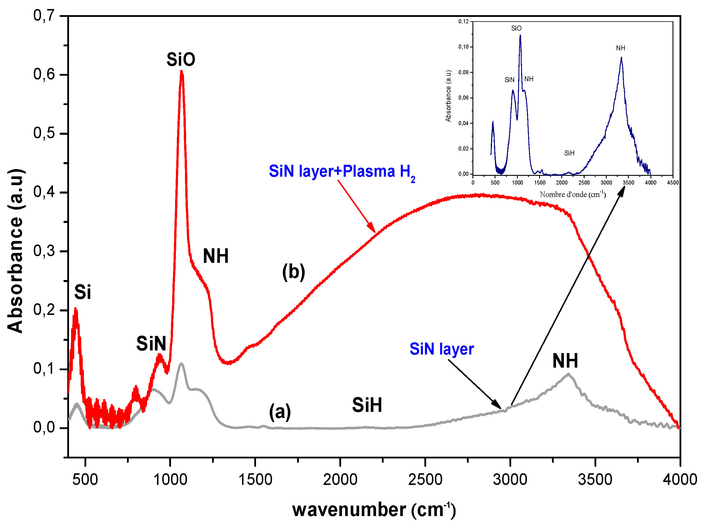
Figure 4.
SEM images of (a) bare mc-Si, (b) T-mc-Si with H2/SiNx and (c) cross-section view T-mc-Si with H2/SiNx.
Figure 4.
SEM images of (a) bare mc-Si, (b) T-mc-Si with H2/SiNx and (c) cross-section view T-mc-Si with H2/SiNx.
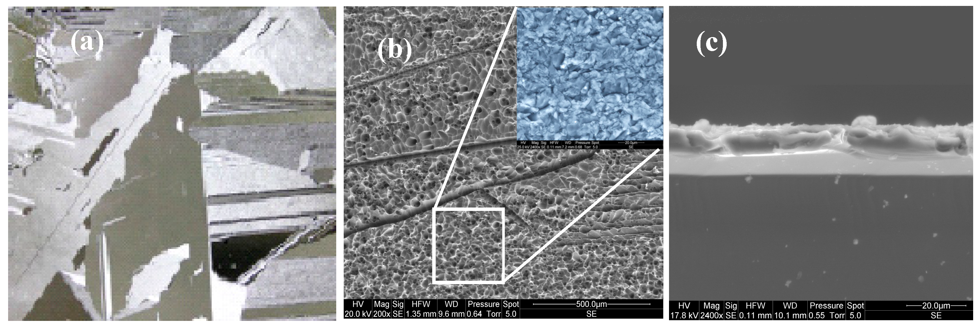
Figure 5.
Total reflectivity of (a) Bare mc-Si (b)T-mc-Si (b) before and (c) T-mc-Si with H2/SiNx.
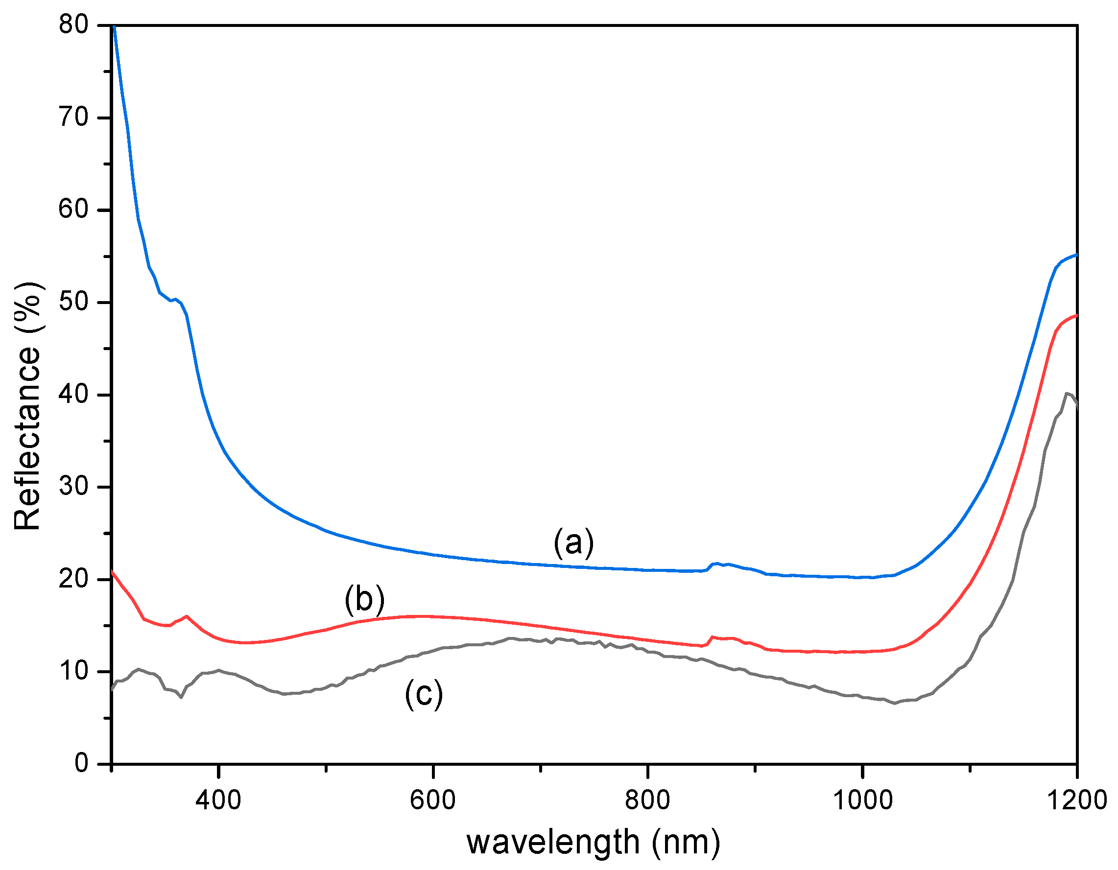
Figure 6.
Mapping of the effective lifetime, diffusion length, and iron concentration of (a) bare mc-Si and (b) T-mc-Si with SiNx/ H2 plasma.
Figure 6.
Mapping of the effective lifetime, diffusion length, and iron concentration of (a) bare mc-Si and (b) T-mc-Si with SiNx/ H2 plasma.
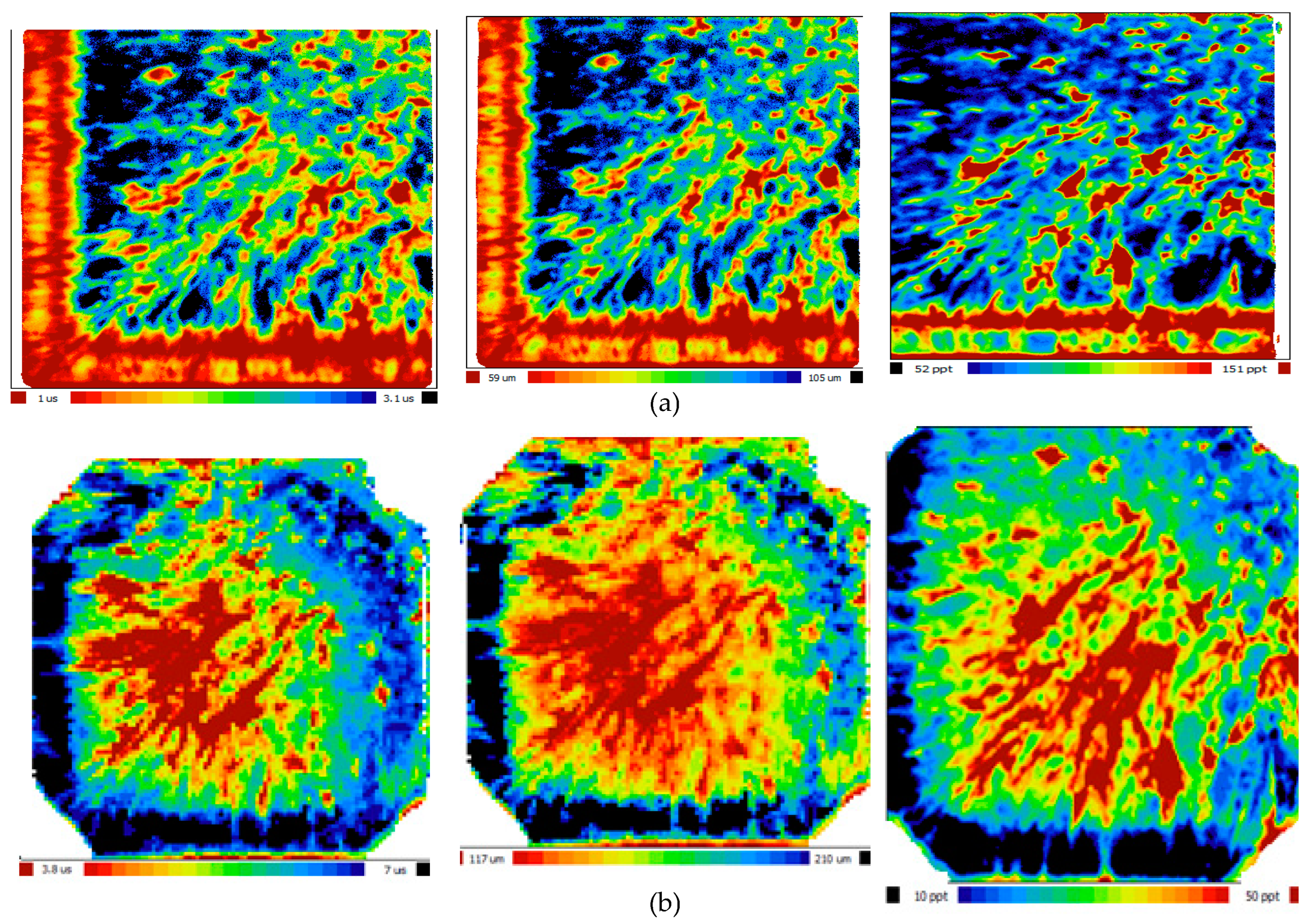
Figure 7.
Mapping of the effective lifetime, diffusion length, and iron concentration of the mc-Si wafer (10 cm × 10 cm) of edges region (a) before and (b) after T-mc-Si.
Figure 7.
Mapping of the effective lifetime, diffusion length, and iron concentration of the mc-Si wafer (10 cm × 10 cm) of edges region (a) before and (b) after T-mc-Si.
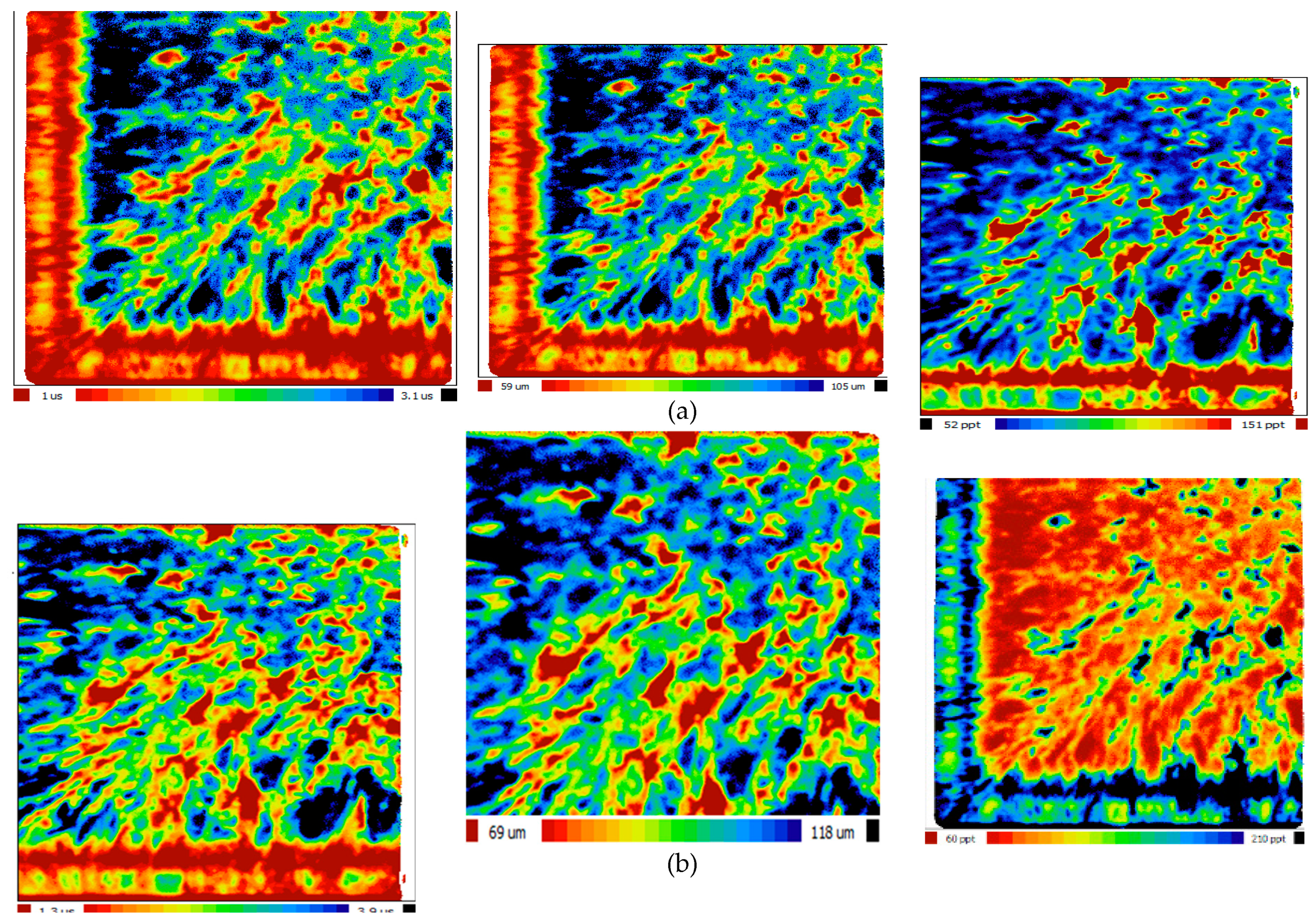

Table 1.
Optimized parameters for the SiNx layer deosition and hydrogen plasma treatment via PECVD.
| Pu (mbar) |
P (mTorr) | T (°C) |
Time (s) |
RF (W) |
SiH4 (sccm) |
NH3 (sccm) | H2 (sccm) | |
| H2 Plasma | 2x10⁻¹ | 700 | 300 | 50 | 60 | - | - | 100 |
| SiNx layer | 2x10⁻¹ | 700 | 300 | 900 | 5 | 3 | 70 | - |
Disclaimer/Publisher’s Note: The statements, opinions and data contained in all publications are solely those of the individual author(s) and contributor(s) and not of MDPI and/or the editor(s). MDPI and/or the editor(s) disclaim responsibility for any injury to people or property resulting from any ideas, methods, instructions or products referred to in the content. |
© 2025 by the authors. Licensee MDPI, Basel, Switzerland. This article is an open access article distributed under the terms and conditions of the Creative Commons Attribution (CC BY) license (http://creativecommons.org/licenses/by/4.0/).
Copyright: This open access article is published under a Creative Commons CC BY 4.0 license, which permit the free download, distribution, and reuse, provided that the author and preprint are cited in any reuse.


