
Submitted:
26 March 2025
Posted:
27 March 2025
You are already at the latest version
Abstract
Surface texturing is vital in enhancing light absorption and optimizing the optoelectronic properties of multicrystalline silicon (mc-Si) samples. Texturing significantly improves light absorption by minimizing reflectance and extending the effective path length of incident light. Furthermore, porous silicon treatment on textured mc-Si surfaces offers additional advantages, including enhanced carrier generation, reduced surface recombination, and improved light emission. In this study, a dual treatment combining porous silicon and texturing was employed as an effective approach to enhance the optical and optoelectronic properties of mc-Si. Both porous silicon and texturing were achieved through a chemical etching process. After these surface modifications, the morphology and structure of mc-Si were examined using Atomic Force Microscopy (AFM), Scanning Electron Microscopy (SEM), UV-Vis-IR spectroscopy, Photoluminescence (PL), WCT-120 photoconductance lifetime measurements, and Internal Quantum Efficiency (IQE) analysis. Results reveal a substantial improvement in the material’s properties. The total reflectivity dropped from 35% to approximately 5%, while the effective minority carrier lifetime increased from 2 µs to 36 µs. Additionally, the two-dimensional IQE value rose from 31% for the untreated sample to 63% after treatment, representing an enhancement of around 26%. These findings highlight the potential of surface engineering techniques in optimizing mc-Si for photovoltaic applications.
Keywords:
silicon
; texturization
; porous silicon
; reflectivity
; lifetime
; two-dimensional IQE
1. Introduction
Multicrystalline silicon (mc-Si) is widely used in solar cells for its cost-efficiency balance [1,2,3,4]. Recent processing advancements aim to enhance its light absorption and electronic for better performance [5,6,7,8]. Among these techniques, double treatments, which combine two different processing methods, have shown significant promise. The ability of silicon to absorb light increases with wavelength. Techniques such as Texturing and anti-reflection coatings [9,10] have been explored to enhance the absorption characteristics of mc-Si. Surface modifications using chemical etching [11] or plasma treatments [12] can significantly reduce light reflectance, increasing the amount of light absorbed by the solar cell. Recent studies have investigated various combinations of treatments to optimize the light absorption and electronic performance of mc-Si. These double treatments typically Texturing and Antireflective Coatings. Surface Texturing enhances light trapping by creating a rough surface that reduces reflectance. For instance, alkaline etching followed by acidic etching has been shown to produce optimal textures. Materials such as silicon nitride and titanium dioxide [13,14] are commonly used as Antireflective Coatings to further minimize reflection losses. Combining Texturing with ARC has demonstrated improved optical absorption and overall cell efficiency. The optoelectronic properties of mc-Si, including charge carrier lifetime, mobility, and junction quality, are crucial for device performance. Double treatments have been shown to improve these properties. Enhanced optical properties often correlate with improved carrier lifetimes. For example, studies report that double treatments can lead to lifetimes exceeding 1 ms, significantly boosting efficiency. Optimizing surface conditions through double treatments can reduce recombination losses at the surface and within the bulk material, enhancing the overall device performance. Silicon used in commercial solar cell fabrication typically contains impurities and defects that negatively impact minority carrier lifetime, thereby reducing cell efficiency. As a result, the photovoltaic (PV) industry is seeking processes that can provide both surface and bulk passivation in c-Si solar cells. Surface texturing plays a critical role in enhancing the optical path length of incident light, and reducing surface reflections, and has become a key feature in solar cell technology. In silicon solar cells, surface texturing is traditionally achieved through chemical etching methods, including both anisotropic and isotropic etching [15,16]. Porous silicon (PS) can be easily formed using the stain etching (SE) technique by immersing crystalline silicon in a solution of HF/HNO3/H2O for an optimized duration [17]. The combination of texturization and PS is a new approach to enhancing the optic and optoelectronics propriety of crystalline silicon. The present work aims to demonstrate mc-Si's optic and optoelectronics propriety, which can be achieved by double treatments; texturization, and porous silicon. Elaborated samples were characterized to investigate the structure, optic, and optoelectronic properties by measuring the Reflectivity, infra-red (IR) absorption, PL, effective lifetime, and two-dimensional internal quantum efficiency.
2. Results
The structural characterization of multicrystalline silicon (mc-Si) is crucial for understanding the impact of NaOH texturization and porous silicon (PS) formation. Scanning Electron Microscopy (SEM) and Atomic Force Microscopy (AFM) offer valuable insights into the surface morphology of mc-Si following these treatments. Chemical Texturing modifies the surface morphology to enhance light trapping and minimize reflectivity. As shown in Figure 1b, the textured surface significantly increases the effective area that interacts with incoming light compared to the reference sample (Figure 1a). This texturization plays a crucial role in improving light absorption in solar cells by inducing multiple internal reflections within the material, thereby increasing photon absorption in silicon. Additionally, textured surfaces capture light at various angles, enhancing absorption under different lighting conditions, including direct sunlight and diffuse light. The rough surface scatters incoming light instead of reflecting it away, promoting diffused reflection and reducing optical losses. During the texturing process, the alkaline solution etches the silicon, resulting in a nanoscale pyramidal structure, as shown in Figure 1b. These structures enhance light scattering and trapping, thereby increasing light absorption in silicon by reducing reflectivity compared to a flat silicon surface. This, in turn, leads to a higher generation of electron-hole pairs. As illustrated in Figure 1b, the micro-sized pyramids significantly increase the effective surface area available for light absorption. Their geometry allows for improved light capture at various angles, which is particularly advantageous under varying lighting conditions. Additionally, the textured surface scatters incoming light, minimizing direct reflection that would otherwise occur on smooth surfaces. The pyramidal structures effectively act as a natural anti-reflective coating, reducing optical losses and enhancing overall light absorption.
The formation of the porous silicon layer on the texturized mc-silicon surface was realized by the stain etching method. This process results in a network of pores that further enhances the material’s properties see Figure 2. The formed pores increase the surface area even more, allowing for better light trapping and absorption. The porous structure can reduce reflectivity even further than what is achieved by Texturing alone, as the irregular surface structure scatters light more effectively. The combination of Texturing and porous silicon results in a synergistic effect, where each method enhances the benefits of the other. The textured surface provides a foundation for effective light trapping, while the porous layer further minimizes reflectivity and improves charge carrier lifetime. Obtained results have shown that mc-Si substrate treated with both chemical texturing and porous silicon layers can achieve significantly higher electronic quality compared to untreated or only textured substrate.
This dual treatment enhances light trapping, reduces surface reflectivity, and provides passivation, which collectively contributes to the greater quality of mc-Si. Optical characterization is essential for evaluating the effectiveness of treatments such as chemical texturing and the addition of a PS layer on the mc-Si wafer. This characterization helps assess light absorption, reflectivity, and overall material quality for solar cell applications. Figure 3 shows optical characterization after different texturization times. First, we carried out an optimization of the surface texturing and measured for each time the reflectivity. For untreated mc-Si, the average reflectivity is about 50-55% in the range of (400-1000 nm). For textured mc-Si, the average reflectivity ranges from approximately 25% to 15% across the same wavelength range, with sharp decreases at specific wavelengths due to enhanced light trapping. The reflectivity spectrum indicates that the optimal etching time to reduce surface reflectivity to 15% is 3.5 minutes. In the next step, a porous silicon layer was added to this textured surface, resulting in a significant decrease in reflectivity. As shown in Figure 4, textured mc-Si with a porous silicon layer further reduces surface reflectivity to approximately 5–10%, this result is better than that reported in [18,19]., thereby improving light absorption. This substantial reduction in reflectivity is attributed to the combined effects of Texturing and porosity, particularly in the UV spectrum, due to the formation of a nano-porous morphology.
It is important to investigate the potential of using PS treatment on textured silicon wafers for photovoltaic applications. To quantify the variation in the electronic quality of the mc-Si before each treatment, we assessed the surface quality of the textured and PS/textured samples by measuring the effective carrier lifetime of mc-Si before and after each treatment (Ref, texturized, and PS/texturized mc-Si wafers). The optoelectronic characterization (lifetime measurement) demonstrates a significant improvement in the performance of multicrystalline silicon due to the combination of chemical texturing and porous silicon treatment. Figure 5 and Table 1 illustrate the effective lifetimes at an injection level of 2x10^13 cm−3, measured using a photoconductivity system (WCT-120). We observed that the effective lifetime of the bare mc-Si wafer was 5 µs, which increased to 10 µs after texturization and 36 µs after PS formation on the textured mc-Si, which is higher than that obtained by HF/HNO3 solutions [20]. The formation of PS appears to remove damage caused by chemical texturing, which eliminates some surface impurities and reduces related surface defects, thus enhancing the effective carrier lifetime. These results suggest a correlation between the increased lifetime value and hydrogen passivation. As shown in Figure 6, the freshly prepared PS exhibits well-defined silicon-hydrogen absorption bands at 905-910 cm−1 and 2087-2106 cm−1 [21], which are associated with groups adsorbed at the extended porous silicon surface. Additionally, Si–O modes at 1065 and 1150 cm−1 can be observed [22]. It is believed that both surface and bulk passivation effects are achieved through hydrogen, which passivates impurities and defects in the surface and bulk silicon [23], thereby increasing the minority carrier lifetime, as demonstrated in Figure 5 and Table 1.
The combination of Texturing and porous silicon results in a synergistic effect, where each method enhances the benefits of the other. The textured surface provides a foundation for effective light trapping, while the porous layer further minimizes reflectivity and improves charge carrier dynamics. Obtained results have shown that mc-Si substrate treated with chemical texturing and porous silicon layers can achieve significantly higher electronic quality than untreated or only textured substrate. The porous silicon layer also serves a crucial role in passivating defects on the silicon surface. The porous structure helps reduce surface states' density, which can trap charge carriers and lead to recombination losses. By passivating the surface, the porous silicon layer enhances the lifetime of charge carriers, leading to improved solar cell efficiency.
The obtained results enable us to correlate the increase in lifetime values with the total reflectivity, as shown in Figure 7. The improvement in lifetime can be attributed to hydrogen passivation, as revealed by the FTIR analysis, as well as the enhanced surface area resulting from both texturization and porous silicon (PS) treatment.
Figure 8 demonstrates the photoluminescence spectra of both textured mc-Si and porous silicon layers at room temperature. The maximum PL peak is observed between 600-650 nm, displaying an intense, Gaussian-like spectrum. An important increase in PL intensity is seen after the PS elaboration, this enhancement is attributed to surface passivation by hydrogen and chemical oxidizing agents, which reduce non-radiative recombination and improve emission efficiency. This result is further confirmed by lifetime measurements. At room temperature, PL spectra provide valuable insights into the thermally activated processes within the material. The intensity and position of the peaks offer information about carrier dynamics and recombination mechanisms. Additionally, variations in excitation power during PL measurements can influence peak intensity, revealing differences in carrier generation and recombination between the textured and PS layers.
To evaluate the effectiveness of the investigated surface passivation methods in high-efficiency silicon solar cells, a simplified passivated emitter structure was fabricated on multicrystalline silicon (mc-Si) substrates, as depicted in Figure 9. The metallization process was designed with a front contact coverage of 2%, ensuring minimal shading losses, while the back surface was entirely metalized (100%) to optimize charge carrier collection. Among the key performance indicators of a solar cell, internal quantum efficiency (IQE) is particularly sensitive to recombination processes within the device. Therefore, our analysis primarily focuses on this parameter. Figure 10 presents the IQE surface mapping using the LBIC technique [24] for mc-Si solar cells, both with and without PS/textured passivation treatment. Before PS treatment (Figure 10a), the IQE ranges from 8% to 35%. After PS treatment (Figure 10b), the minimum IQE increases to 54%, and the maximum value reaches 66%, reflecting a 31% improvement. This enhancement confirms the effectiveness of the passivation technique in reducing surface recombination and improving device performance [25]. The significant improvement is attributed to the combined effects of surface texturization, which reduces reflectivity, and chemical passivation through Si-O and Si-H bonds in the porous silicon layer, this result is good compared to that of porous aluminum/silicon nanostructures [26]. The increase in internal quantum efficiency correlates with a rise in effective lifetime from 5 to 36 µs, driven by hydrogen passivation and chemical oxidizing agents., which reduce surface states' density, trap charge carriers, and lead to recombination losses. This result is confirmed by lifetime and PL measurements. The findings presented in this study confirm that the PS/textured surface passivation technique significantly enhances the performance of mc-Si solar cells by improving front surface passivation and reducing recombination losses. These results demonstrate the strong potential of PS/textured passivation as an advanced strategy for achieving higher-efficiency mc-Si solar cells.
Based on Figure 10, we constructed the histogram shown in Figure 11, which illustrates the IQE mapping frequency as a function of IQE for the same sample before and after PS/texturization treatment on mc-Si. For the PS-treated texturized sample (b), the histogram shifts to higher IQE values. The IQE range increases from 47–48% for the bare mc-Si to 46–64% for the PS-treated texturized sample, highlighting the significant improvement in the treated mc-Si sample electronic quality.
4. Materials and Methods
This experimental method aims to enhance the optical and optoelectronic properties of mc-Si by combining texturization and porous silicon (PS) formation. The approach seeks to improve light absorption and reduce surface recombination in the mc-Si wafer. The material used is a p-type mc-Si wafer with a resistivity of 0.5–2 Ω·cm and an area of 1 cm x 1 cm. First, organic contaminants are removed by cleaning the mc-Si wafers in hydrochloric acid (HCl) and hydrogen peroxide (H2O2) for 10 minutes, followed by thorough rinsing with deionized water and drying with nitrogen. The mc-Si substrate is then texturized by immersing it in a 1 M NaOH solution at 80°C for varying etching times. Etching time was selected based on reflectivity spectrum analysis to optimize the texturization process. After NaOH texturization, the mc-Si substrate undergoes PS formation using the stain etching (SE) method. PS is formed on the texturized mc-Si by dipping the wafer in a 1:3:5 mixtures of HF (48 wt%), HNO3 (65 wt%), and H2O for 20 minutes. After etching, the PS-treated sample is washed with deionized water and dried under a nitrogen gas. The composition of the PS on the texturized mc-Si surface was analyzed using FTIR (Nicolet MAGNA 560). Photoluminescence (PL) measurements were performed with an argon laser (4765 Å). Photo-carrier lifetimes were measured using the WCT-120 photoconductivity system (in the range 10 ns to 10 ms). Surface morphology was analyzed by Atomic Force Microscopy (AFM) and Scanning Electron Microscopy (SEM). Reflectivity spectra were obtained using a LAMBDA 950 UV/Vis/NIR Spectrophotometer with an integrating sphere (in the range 350-1100 nm). Finally, two-dimensional internal quantum efficiency (IQE) distribution was measured with the LBIC technique.
5. Conclusions
This study demonstrates that Stain Etching-based porous silicon (PS) formed on textured multicrystalline silicon (mc-Si) enhances surface lifetime, photoluminescence, and reduces reflectivity.
In summary, optical and optoelectronic characterization of mc-Si with a combined porous silicon/texturized layer reveals significant improvements in electronic quality. Chemical texturing and PS formation effectively reduce reflectivity from 55% to 5%, significantly increasing light absorption across the visible spectrum. Additionally, the porous silicon layer enhances passivation through hydrogen incorporation, leading to an increase in carrier lifetime from 1 to 36 µs at a minority carrier density (Δn) of 10¹⁵ cm⁻³, while the internal quantum efficiency (IQE) improves from 35% to 66%, reflecting a 31% improvement. These findings highlight the potential of surface engineering techniques in optimizing mc-Si for photovoltaic applications, paving the way for more efficient and cost-effective solar energy solutions. Future research should focus on refining these treatments and integrating them into commercial solar cell manufacturing.
Author Contributions
All authors contributed to the study's conception and design. Conceptualization, M.B.R., Y.Z., and A.E.H.; methodology, A.M.; software, K.C.; validation, M.A.A., W.D. and M.B.R.; formal analysis, A.E.H., and Y.Z.; investigation, A.M.; resources, K.C.; data curation, M.A.A.; writing—original draft preparation, W.D.; writing—review and editing, M.B.R.; visualization, K.C.; supervision, M.B.R.; project administration, K.C.; funding acquisition, K.C. All authors have read and agreed to the published version of the manuscript.
Funding
This work was supported and funded by the Deanship of Scientific Research at Imam Mohammad Ibn Saud Islamic University (IMSIU) (grant number IMSIU-DDRSP2502.
Data Availability Statement
The datasets generated during and/or analyzed during the current study are available from the corresponding author upon reasonable request.
Conflicts of Interest
The authors declare no conflicts of interest.
References
- Schindler, F.; Michl, B.; Krenckel, P.; Riepe, S.; Benick, J.; Müller, R.; Schubert, M. C. Optimized multicrystalline silicon for solar cells enabling conversion efficiencies of 22%. Solar energy materials and solar cells 2017, 171, 180-186. [CrossRef]
- Schindler, F.; Fell, A., Müller, R.; Benick, J.; Richter, A.; Feldmann, F.; Glunz, S. W. Towards the efficiency limits of multicrystalline silicon solar cells. Solar Energy Materials and Solar Cells 2018, 185, 198-204. [CrossRef]
- Möller, H. J.; Funke, C.; Rinio, M.; Scholz, S. Multicrystalline silicon for solar cells. Thin solid films 2005, 487(1-2), 179-187.
- Gurusamy, A.; Manickam, S.; Perumalsamy, R.: Quality improvement of multi-crystalline silicon ingot by the Hot-Zone modification. J. Cryst. Growth 2022, 592, 126720. [CrossRef]
- Koynov, S.; Brandt, M. S.; Stutzmann, M. Black multi-crystalline silicon solar cells. physica status solidi (RRL)–Rapid Research Letters 2007, 1(2), R53-R55.
- Alrasheedi, N. H. The effects of porous silicon and silicon nitride treatments on the electronic qualities of multicrystalline silicon for solar cell applications. Silicon 2024, 16(4), 1765-1773. [CrossRef]
- Rabha, M. B.; El Haj, A.; Mannai, A.; Choubani, K.; Almeshaal, M. A.; Dimassi, W. Optoelectronic proprieties improvement of multicrystalline silicon by Alumina Nanoparticles and silicon nitride.2025. [CrossRef]
- Park, K. M.; Jung, J. H.; Hong, J. E.; Choi, S. Y.; Lee, M. B. RIE Texturing Optimization for Multicrystalline Silicon Solar Cell. In ECS Meeting Abstracts (No. 1, p. 62). IOP Publishing 2010. [CrossRef]
- Valiei, M.; Shaibani, P. M.; Abdizadeh, H.; Kolahdouz, M.; Soleimani, E. A.; Poursafar, J. Design and optimization of single, double and multilayer anti-reflection coatings on planar and textured surface of silicon solar cells. Materials Today Communications 2022, 32, 104144.
- Solanki, C. S.; Singh, H. K.; Solanki, C. S.; Singh, H. K. Anti-reflection Coatings with Textured Surface for c-Si Solar Cells. Anti-reflection and Light Trapping in c-Si Solar Cells 2017, 99-114.
- Solanki, C. S.; Singh, H. K.; Solanki, C. S.; Singh, H. K. Anti-reflection Coatings with Textured Surface for c-Si Solar Cells. Anti-reflection and Light Trapping in c-Si Solar Cells 2017, 99-114.
- Yoo, J.; Cho, J.; Han, K.; Yi, J. RIE surface texturing for optimum light trapping in multicrystalline silicon solar cells. Journal of the Korean Physical Society 2012, 60, 2071-2074. [CrossRef]
- Yousuf, H.; Rahman, R. U.; Jang, S.; Rehan, S.; Khokhar, M. Q.; Park, S.; Yi, J. Enhanced hydrogenated silicon nitride (SiNx: H) thin film as single layer anti-reflection (SLAR) coating in tunnel oxide passivated contact solar cells. Materials Science in Semiconductor Processing 2025, 192, 109483. [CrossRef]
- Rathinavelu, V.; Upadhyay, V. V.; Prabagaran, S.; Govindarajan, S.; Verma, A.; Soudagar, M. E. M.; Seikh, A. H. Texturing of silicon nitride passivation layers on functional behaviour study of polycrystalline silicon (p-Si) made with plasma enhanced chemical vapour deposition. Journal of Materials Science: Materials in Electronics 2025, 36(1), 73. [CrossRef]
- Çiftci, B. G.; Güldür, Ç.; Güneş, S. (2025). Inverted Pyramid Texturization of Monocrystalline Silicon Surface by Cu-Assisted Chemical Etching at Different Conditions. Silicon 2025, 1-10. [CrossRef]
- Stapf, A.; Gondek, C.; Kroke, E.; Roewer, G. Wafer cleaning, etching, and texturization. Handbook of Photovoltaic Silicon 2019, 311-358.
- Raji, M.; Gurusamy, A.; Manikkam, S.; Perumalsamy, R. Monocrystalline Silicon Wafer Recovery Via Chemical Etching from End-of-Life Silicon Solar Panels for Solar Cell Application. Silicon 2024, 16(9), 3669-3688.. [CrossRef]
- Marrero, N., Guerrero-Lemus; R., Gonzalez-Diaz, B.; Borchert, D. Effect of porous silicon stain etched on large area alkaline textured crystalline silicon solar cells. Thin Solid Films 2009, 517(8), 2648-2650. [CrossRef]
- Bilyalov, R. R.; Lüdemann, R.; Wettling, W.; Stalmans, L.; Poortmans, J.; Nijs, J.; Lévy-Clément, C. Multicrystalline silicon solar cells with porous silicon emitter. Solar energy materials and solar cells 2000, 60(4), 391-420. [CrossRef]
- Montesdeoca-Santana, A.; Gonzalez-Diaz, B.; Jiménez-Rodríguez, E.; Ziegler, J.; Velázquez, J. J.; Hohage, S.; Guerrero-Lemus, R. Influence of stain etching on low minority carrier lifetime areas of multicrystalline silicon for solar cells. Materials Science and Engineering: B 2011, 176(18), 1541-1545. [CrossRef]
- Gupta, I.; Colvin; V. L.; George; S. M. Hydrogen desorption kinetics from monohydride and dihydride species on silicon surfaces. Physical Review B 1988, 37(14), 8234. [CrossRef]
- Montero, I.; Galan, L.; Najmi, O.; Albella, J. M. (1994). Disorder-induced vibration-mode coupling in SiO2 films observed under normal-incidence infrared radiation. Physical Review B 1994, 50(7), 4881.
- Rabha, M. B.; Bessaïs, B. (2010). Enhancement of photovoltaic properties of multicrystalline silicon solar cells by combination of buried metallic contacts and thin porous silicon. Solar Energy 2010, 84(3), 486-491. [CrossRef]
- Rabha, M. B.; Dimassi, W.; Bouaïcha, M.; Ezzaouia, H.; Bessais, B. Laser-beam-induced current mapping evaluation of porous silicon-based passivation in polycrystalline silicon solar cells. Solar Energy 2009, 83(5), 721-725. [CrossRef]
- Abdouli, B.; Khezami, L.; Guesmi, A.; Assadi, A. A.; Rabha, M. B. Numerical and experimental study of the front surface recombination velocities and base widths effect in multi-crystalline silicon solar cell quantum efficiency. Crystals 2023; 13(3); 425. [CrossRef]
- Achref, M.; Khezami, L.; Mokraoui, S.; Rabha, M. B. Effective surface passivation on multi-crystalline silicon using aluminum/porous silicon nanostructures. Surfaces and Interfaces 2020, 18, 100391. [CrossRef]
Figure 1.
SEM and AFM images of (a) bare and (b) textured mc-Si.
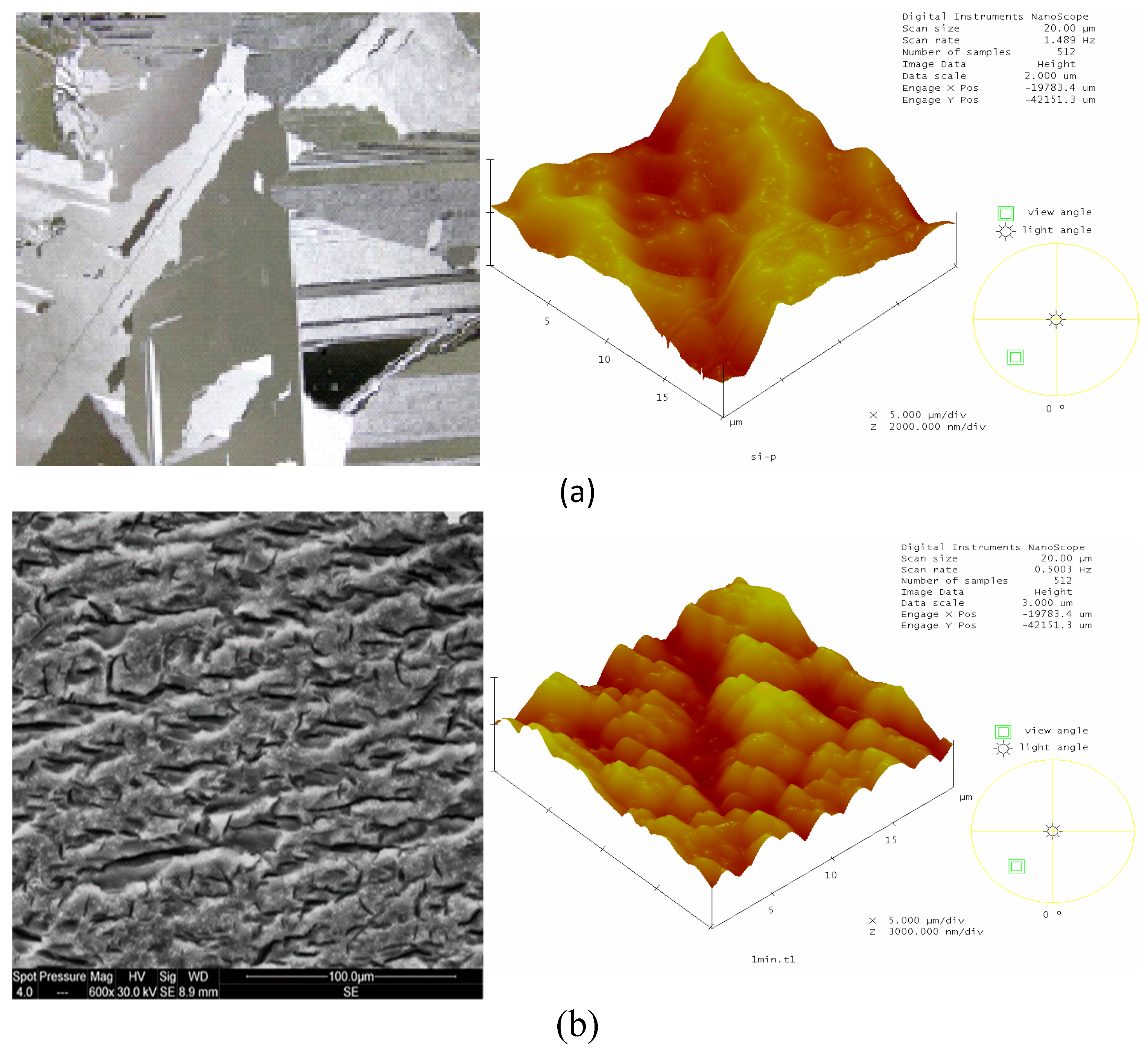
Figure 2.
SEM and AFM images of a texturization mc-Si with PS.
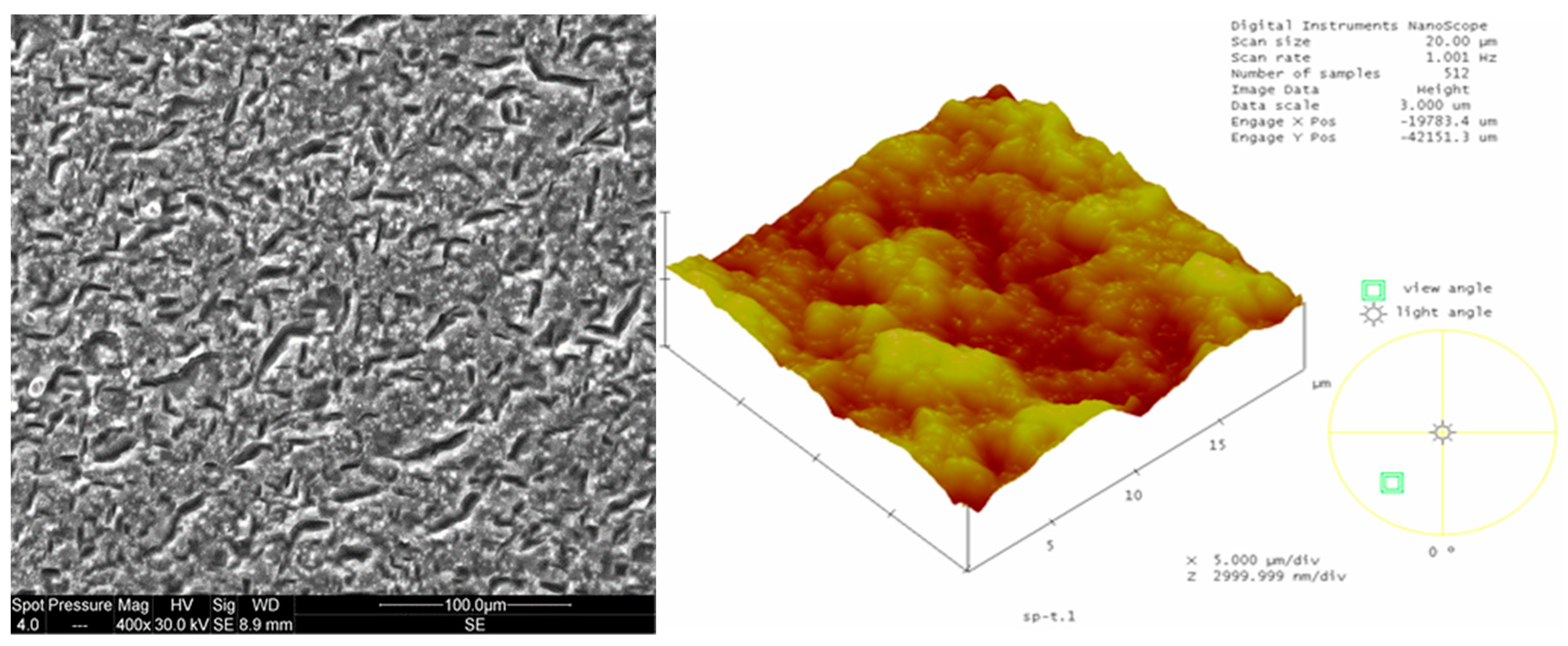
Figure 3.
Variation of the surface reflectivity of mc-Si for different texturization times.
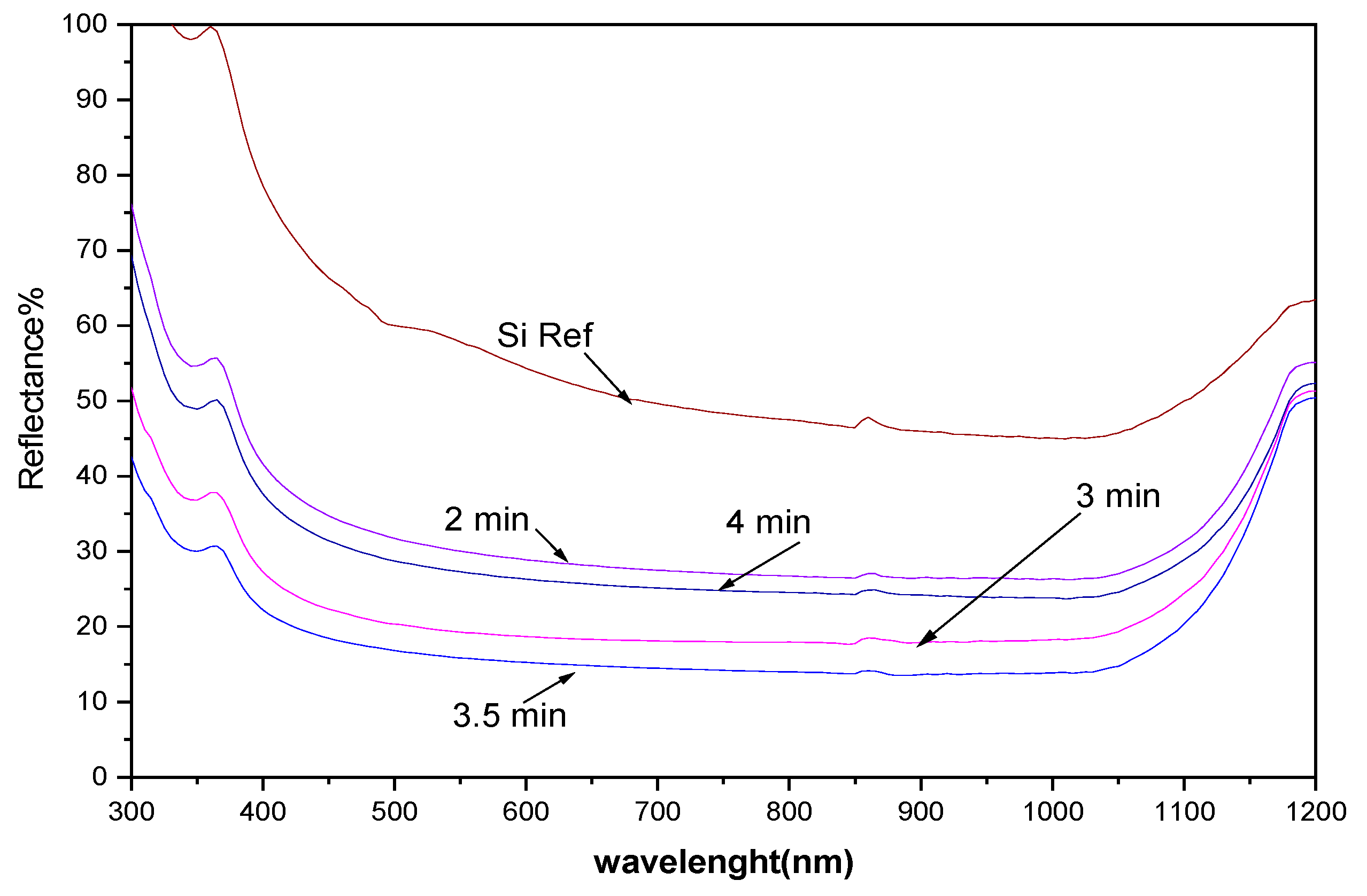
Figure 4.
Surface reflectivity of (a) textured mc-Si and (b) PS /Textured mc-Si compared to ref mc-Si.
Figure 4.
Surface reflectivity of (a) textured mc-Si and (b) PS /Textured mc-Si compared to ref mc-Si.
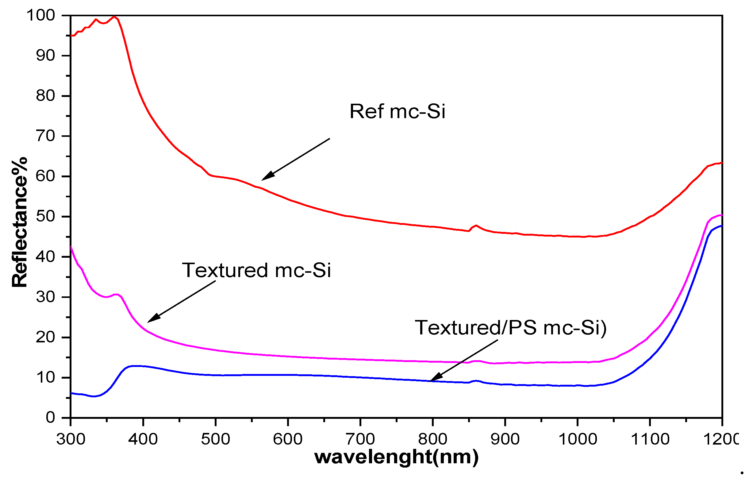
Figure 5.
Evolution of mc-Si lifetime for various processes.
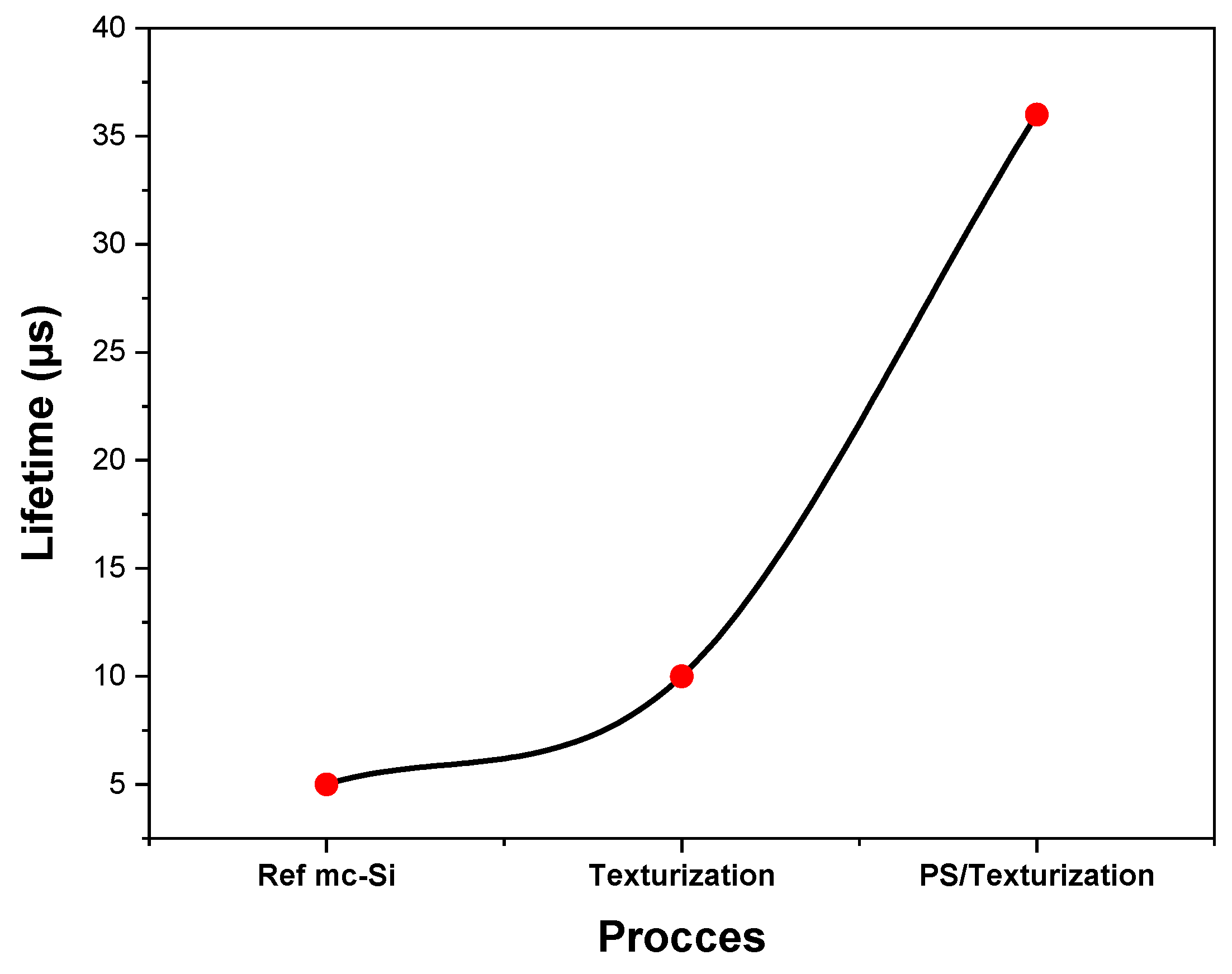
Figure 6.
FTIR spectra of PS prepared by SE method.
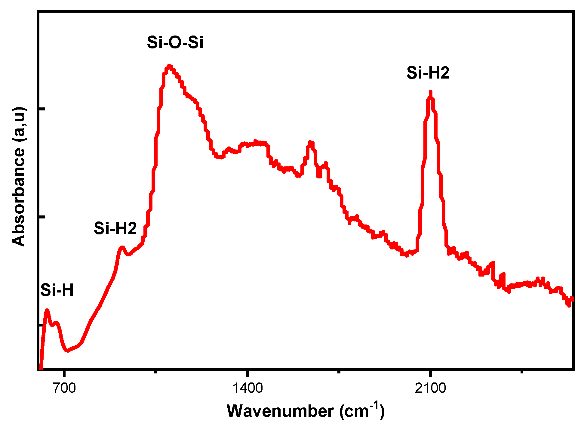
Figure 8.
Correlation between (a) effective lifetime versus total reflectivity for various processes of mc-Si.
Figure 8.
Correlation between (a) effective lifetime versus total reflectivity for various processes of mc-Si.
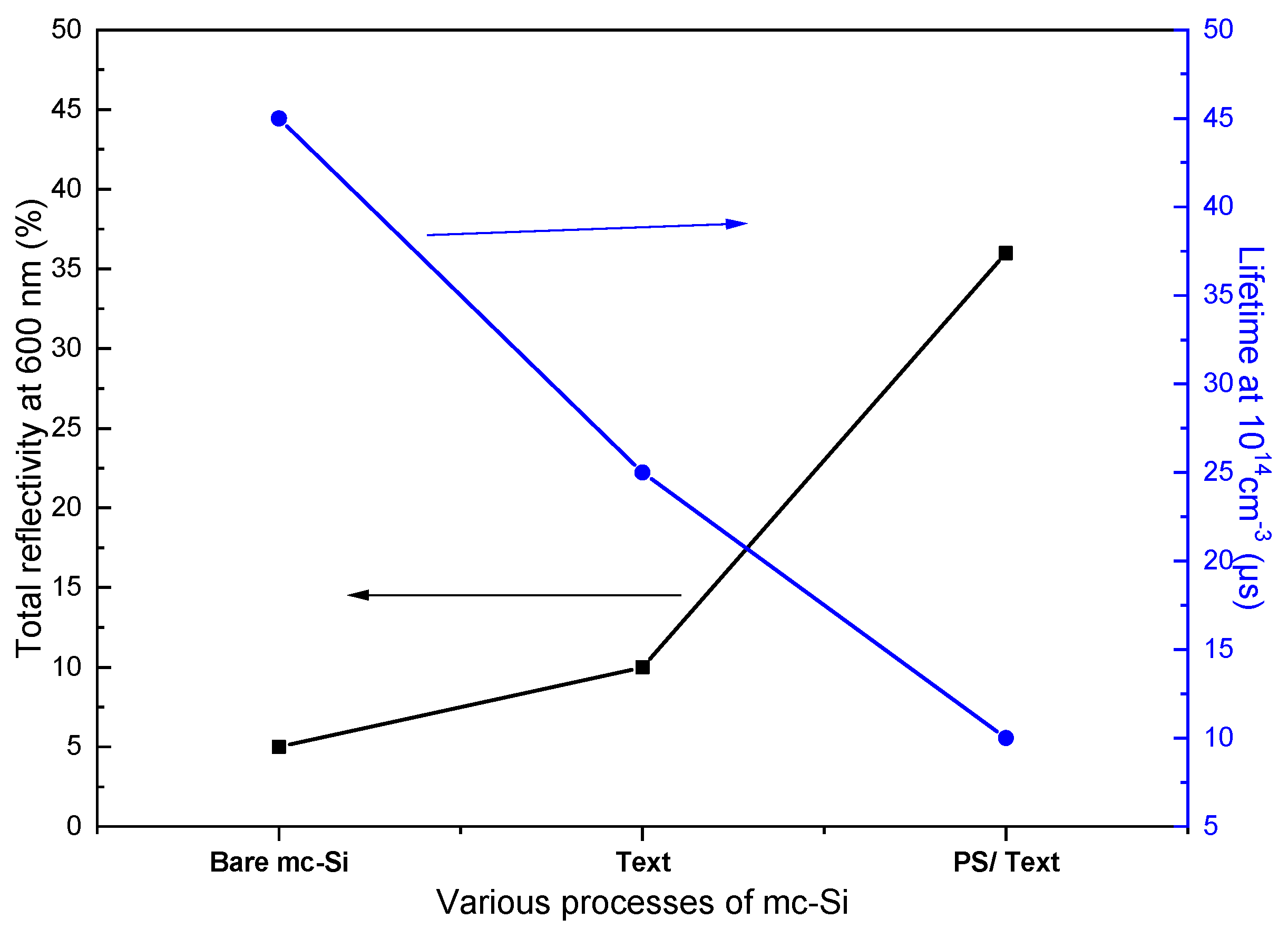
Figure 8.
PL spectra of the texturized mc-Si sample before and after PS treatment.
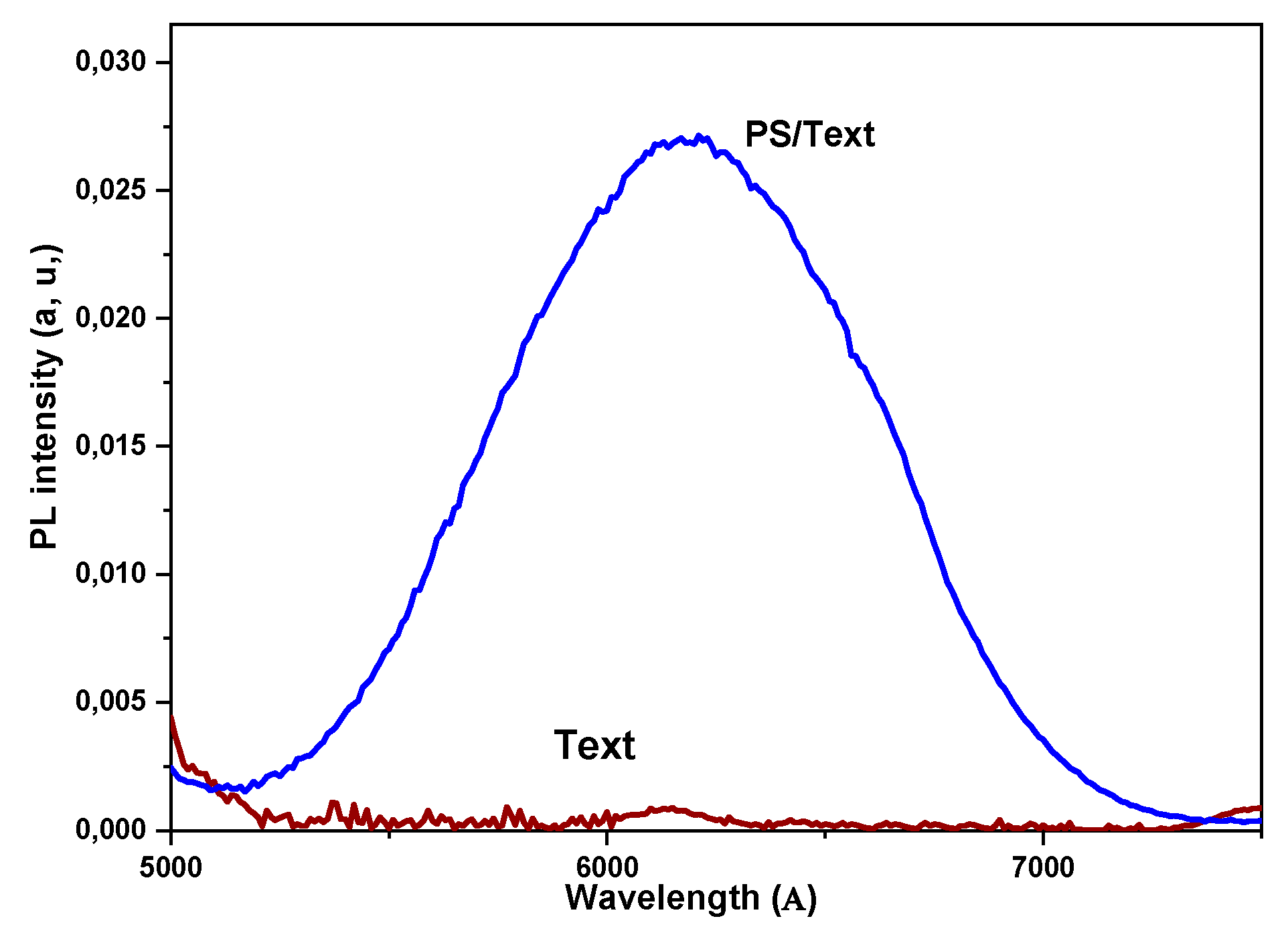
Figure 9.
Schematic diagram of a textured mc-Si solar cell with PS layer.
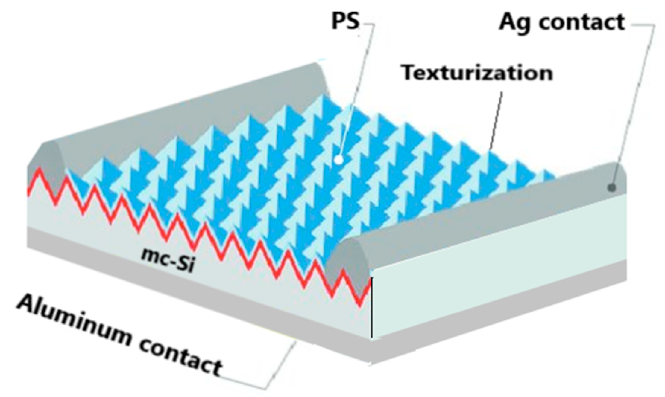
Figure 10.
Two-dimensional distribution of IQE) (a) before and (b) after treatment.

Figure 11.
IQE Histograms (a) Before and (b) After PS/Texturization Treatment of mc-Si.
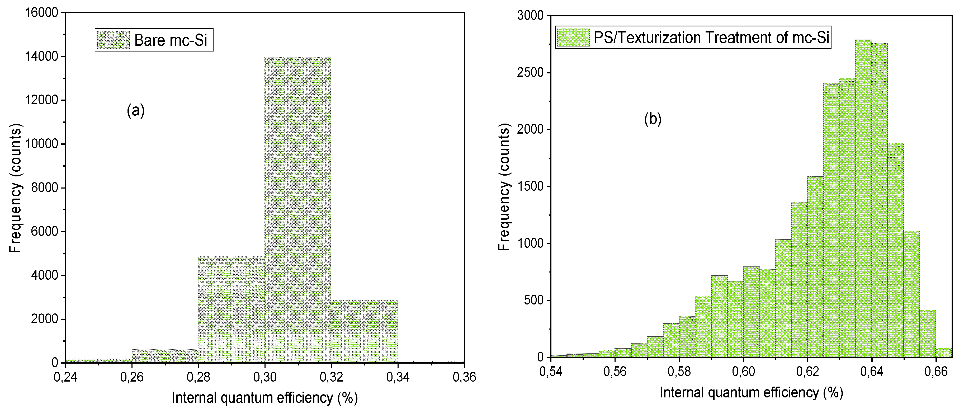

Table 1.
Evolution of mc-Si Lifetime After Various Treatments at an Injection Level of 2x10^13 cm−3.
Table 1.
Evolution of mc-Si Lifetime After Various Treatments at an Injection Level of 2x10^13 cm−3.
| Process | Bare mc-Si | Texturized mc-si | Texturized/PS |
|---|---|---|---|
| Lifetime (µs) | 5 | 10 | 36 |
Disclaimer/Publisher’s Note: The statements, opinions and data contained in all publications are solely those of the individual author(s) and contributor(s) and not of MDPI and/or the editor(s). MDPI and/or the editor(s) disclaim responsibility for any injury to people or property resulting from any ideas, methods, instructions or products referred to in the content. |
© 2025 by the authors. Licensee MDPI, Basel, Switzerland. This article is an open access article distributed under the terms and conditions of the Creative Commons Attribution (CC BY) license (https://creativecommons.org/licenses/by/4.0/).
Copyright: This open access article is published under a Creative Commons CC BY 4.0 license, which permit the free download, distribution, and reuse, provided that the author and preprint are cited in any reuse.


