
Submitted:
24 November 2024
Posted:
25 November 2024
You are already at the latest version
Abstract
Black silicon has attracted significant interest for various engineering applications, including solar cells, due to its ability to create highly absorbent surfaces or interfaces for light. It enhances light absorption in crystalline solar cells, improving the conversion efficiency of incident light into electricity for photovoltaic applications. This research focuses on fabricating nanostructures that play a critical role in enhancing light absorption on the upper layers of solar cells. These nanostructures were created using the black silicon method, forming a layer known as "black silicon." The coating not only improved the efficiency of crystalline solar cells but also enhanced their stability. The antireflection coating, composed of nanostructures with various shapes including conical, pillar-like, and spike-like forms achieved a reflectivity as low as 10% in the spectral range of 400–700 nm. This corresponded to a sample with α = 0.85 in 4W. An Inductively Coupled Plasma Reactive Ion Etching (ICP RIE) machine was employed to develop and control the specific shape, size, and density of the fabricated black silicon, which was then subjected to testing.
Keywords:
Black silicon
; antireflection coating
; solar cells
; inductively coupled plasma reactive ion etching
1. Introduction
Over the past decade, the increasing demand for renewable energy, particularly solar energy, has driven significant advancements in silicon solar cell technologies for efficient energy harvesting. Today, silicon-based solar cells dominate the commercial market, accounting for approximately 80% of production. This prevalence is attributed to silicon's abundance, cost-effectiveness, and well-established fabrication methods [1,2,3]. As the second most abundant element on Earth, silicon plays a crucial role in semiconductor technology, microelectronics, and nanotechnology. Its widespread availability, coupled with mature manufacturing processes, makes it indispensable for applications requiring high efficiency, flexibility, and cost-effectiveness, such as optoelectronics, photonics, biosensors, and semiconductor devices [4,5,6,7,8,9,10]. Furthermore, silicon-based composite materials have been employed as self-cleaning surfaces, reducing efficiency losses in solar cells, lowering cleaning costs, and maintaining surface stability [11,12,13,14,15]. Recently, alongside the development of deterministic fabrication techniques, a wide range of self-organized methods for creating silicon nanostructures has emerged [16,17,18,19,20,21]. Recent developments in nanotechnology, particularly lithography, have enabled the creation of nanoscale features with unprecedented precision. Techniques such as Extreme Ultraviolet Lithography (EUV) [22], Electron Beam Lithography (EBL) [22, 23], and Nano Imprint Lithography (NIL) [24], combined with precise thin-film deposition methods, facilitate the fabrication of microelectronic devices at the nanometer scale. Many of these structures, produced using methods such as vapor-liquid-solid (VLS) growth or wet-chemical catalytic etching, are commonly referred to as "silicon nanowires," whereas structures created through dry etching are typically known as "black silicon" [16, 17]. With advancements in these processes, etching techniques such as Inductively Coupled Plasma Reactive Ion Etching (ICP RIE) have also evolved, becoming essential for the precise construction and control of multilayer patterns [25].
In this research work, the ICP RIE technique was employed to fabricate black silicon nanostructures for solar cell applications. Comparing the different attempts of nanostructure formation etching method offers several advantages, including precise Nano-structuring, low reflectivity levels in the 400–700 nm spectral range, the ability to produce a variety of surface textures, and improved photovoltaic conversion efficiencies. Additionally, ICP RIE enhances the long-term stability of solar cells and reduces recombination losses, contributing to improvement of the overall performance efficiencies. Based on it, plasma etching method was chosen for its speed, precision, and superior controllability compared to conventional grating techniques [26]. By utilizing reactive species generated in a plasma via a radio frequency (RF) electric field, this method enables the controlled formation of nanostructures with specific shapes and dimensions.
This paper presents the fabrication and characterization of black silicon antireflection coatings for solar cell applications. These coatings consist of nanostructures in various shapes, including conical, pillar-like, and spike formations, produced using the ICP RIE technique. The shape, size, and density of the black silicon nanostructures were characterized using Scanning Electron Microscopy (SEM). Additionally, reflectivity tests, the Bosch process, and Water Contact Angle (WCA) measurements were conducted to evaluate the performance of the fabricated structures.
2. Experimental Setup and Measurements
During the fabrication process of black silicon, a range of devices was employed for sample handling, inspection, and data acquisition. Key tools included the Scanning Electron Microscope (SEM) and the Inductively Coupled Plasma Reactive Ion Etching (ICP RIE) system. In the final stage, Water Contact Angle (WCA) measurements were conducted to evaluate the hydrophobicity of the black silicon surface, including samples processed using the Bosch technique [27,28,29,30]. All ICP RIE plasma etching procedures were carried out in a Class 100 cleanroom environment, utilizing appropriate chemicals and tools to minimize contamination risks [29, 31]. Nano-structural analysis of the fabricated samples was subsequently performed using SEM. Afterward, spectrometer analysis to measure reflectivity and absorption was conducted outside the cleanroom environment. Figure 1 provides an overview of the experimental setup stages used in the fabrication of black silicon.
In the initial stage of this research work, black silicon was fabricated on a clean silicon wafer using a plasma machine. The objective was to examine differences at the microstructural level and evaluate the behavior of black silicon on the surface of a raw silicon wafer. The first samples were created by varying the gas ratio of SF₆ and O₂ in the ICP RIE machine, guided by reference values from previous studies on black silicon [28]. Subsequent samples were fabricated using gas ratios similar to the initial ones, with feedback from the results informing adjustments to the next recipe as can be seen in the Figure 2.
In the early stages of black silicon characterization, sample selection was initially based on the quality of the SEM images, followed by reflectivity measurements. The criteria for SEM analysis focused on the regularity of the microstructures, as well as the size and density of the holes, which are key factors influencing light scattering. As the process progressed, reflectivity measurements were added as additional criteria to aid in sample selection, streamlining the process.
It is important to note that, during the fabrication, some samples had to be reprocessed due to contamination or issues with thermal conductivity in the ICP RIE machine. To mitigate these issues, cleaned samples were prepared from raw silicon wafer cuts. After the cuts were made, the samples were placed in three separate beakers containing acetone, isopropanol, and distilled water. Each solution was applied for three minutes, and the samples were then dried by blowing air onto their surfaces. These samples were then subjected to further analysis in the ICP RIE machine.
The results and challenges encountered at each stage of the process will be discussed in the following sections. The analysis begins with the test samples used to understand the properties of black silicon and measure feature sizes, which will be compared with other samples. For each stage, the final sample results were stored and incorporated into later stages to refine the process and produce high-quality samples based on the original recipe. The accompanying images will help illustrate the "surface nature" of each sample produced, reflecting the specific gas and power combinations used, which are the main variables in this process.
(a) (b)
2.1. First Stage
In the first stage, the structural analysis of the black silicon was conducted, and SEM images were acquired to characterize the samples. The process was carefully documented with a focus on the geometric shape and size of the microstructures formed on the silicon surface. This step aimed to understand how the gas ratio of SF₆ and O₂ influences the geometry of the microstructures after the etching process.
The process began in the plasma machine, where only one variable was initially adjusted: the ratio of sulfur hexafluoride (SF₆) to oxygen (O₂). This ratio was set according to a recipe derived from previous research on black silicon [31]. Once the samples were prepared in the plasma machine, visual inspection via SEM was carried out. The images acquired during this inspection are shown in Figure 3.
2.2. Second Stage
In the second stage, five samples were prepared and analyzed following the steps outlined in the working schedule. One of these five samples was saved to serve as the basis for the next recipe in the following stage. The remaining samples underwent reflectivity testing, and ultimately, only the best-performing sample was selected for comparison in the later stages. The rationale for preparing five samples and selecting the best one was to identify the trends in the structures as the gas ratio changed according to an exponential function. This process began with the previous optimal recipe (α = 0.9), and the gas ratio was adjusted by either increasing or decreasing the amount of gases in a manner that approximates an exponential law, aiming to optimize the recipe more efficiently. The results were based on SEM images of all the samples treated with the gas ratios outlined in Table 1.
The SEM images from this stage are shown in Figure 4 where top and side view of five samples, along with reflectivity data will be shown.
From the top-view SEM images, the best samples with a gas ratio of α = 0.9 exhibited more regular structures, and the hole shapes were more circular. After analyzing the top-view images based on the criteria of regularity, size, and shape, a similar assessment was conducted on the side-view images, which were obtained after cutting the samples with a diamond tip. The sample with α = 0.9 proved to be the best in terms of structural regularity. For further details, the side-view images of all five samples are shown in Figure 5.
For the side-view SEM images of the black silicon samples revealed that the sample with α = 0.9 exhibited the best nanostructures. This sample was identified as the most consistent among the others. To further investigate the shape, size, and relationship of the pillars to light absorption rates, Image was used to measure the dimensions of the pillars. The results are presented in Figure 6.
2.3. Third Stage
On the third stage four new samples were derived from the best one (α=0.9), during first selection. Then from this recipe two best samples got extracted, for this case the SEM and reflectivity test were done. Gas ratios that has been derived from recipes are shown in the Table 2.
The results given by the SEM inspection of the top view and side view after applying the derived recipes into the ICP RIE machine are shown in the Figures 9–12.
From the SEM image acquired is evident that in both cases the microstructure is created (between the ‘holes’) are spread across the sample with the same density, and their size is roughly the same in all the regions. Though for sample with α=0.75 the structures are more regular and deeper, whereas on the right image of the sample with α=0.7 then the microstructures are poorer and not sharp. To compare with the other two samples out of four created another set of SEM image was taken on Figure 9 then send them for the reflectivity test, where both data combined from SEM and reflectivity could give a better result which sample is the best.
Respectively, for the side view the same procedure was done by cutting the samples after the top view done on SEM and after comparing the images, based on such features like geometry of the grating, size, density etc. for the reflectivity measurements.
In the Figure 10 are shown the SEM images from the side view of the samples with a lower ratio respectively α=0.75 and α=0.7 and the different in size between pillars is very small. Furthermore, it is quite hard to understand which one has the lowest reflectivity rate.
In the Figure 11, the pillars ‘coming out’ of the surface can be seen and same result is shown in the images from recipe α=0.8 - 0.85 are combined. Since the gas ratio between the recipes was small, this made the visual inspection hard to decide for the best sample. But going with the reflectivity rate it is more evident the light absorption scale in the samples.
It’s possible to see that the top and side view images of these samples are clearer and the grating is more uniform across the area of the sample though between them; considering the images taken from the side view are evident some differences in terms of size and distribution of the trenches. Thought based on the images it is quite difficult to judge which sample(s) is the best and to avoid uncertainty to select the best sample, the reflectivity measurement took place.
Furthermore, the ratio of gases combined in ICP RIE during etching process, results in different etching profiles due to the selectivity and dynamic of the process, influenced by the dominance or absence of one of the gases either SF6 or O2. Having more O2 in the system will inhibit the etching process, thus increasing SF6 level to stabilize the process and make it etch the silicon surface.
The opposite case is when there is a high amount of SF6 gas, which will lead to a situation where the passivation layer will not be able to provide micro masks necessary to form the black silicon. For these reasons, finding the right equilibrium is theoretically easy to calculate but in practice is difficult to control and is difficult to understand the real process variables acting during the etching process. At this stage the reflectivity levels were quite close as were closed also their ratio of gasses, see Figure 13. All these considerations took the analysis to choose the part of the second stage gas ratios for the next samples.
2.4. Fourth Stage
This step of the work was to find the best possible recipe to minimize the reflectivity level and, at this stage was introduced another variable to control: the chuck bias. The chuck bias, together with gas ratio, contributed with an additional change in the variables of the black silicon fabrication. Gas ratios that has been derived from recipes are shown in the Table 3.
After all the recipes were executed, respectively with the ratios specified and including all the variables, was possible to acquire the following images from SEM, see Figures 14–17.
Figure 14 shows the top view of the SEM images for the three samples with different bias power levels. Impurities can be observed in the samples, likely caused by ions impacting the surface and irregularities in the silicon crystal structure. Despite these imperfections, the pillar-like structures appear relatively regular at the 1 µm scale. However, it is difficult to determine from the top view alone which sample would exhibit the lowest reflectivity or the best light absorption rate.
Figure 15 presents the top views of samples with a gas ratio of α=0.85, treated at three different chuck bias power levels (2, 4, and 6W). Microscale results for this second recipe set show similar outcomes. Cracks and incomplete structures are visible at the corners of the samples, which sometimes complicate the acquisition of clear side-view images. Despite these issues, the top views still appear similar across the samples.
Figure 16 and Figure 17 display the side view images for each gas ratio combination. These images were taken under suboptimal conditions known as "static charge buildup," which causes blurriness due to interference with backscattered electrons. This affects the reflected electron energy, leading to image noise. However, despite the challenges, most of the side-view images still have acceptable quality for SEM analysis. Finally, the reflectivity data shown in Figure 18 and Figure 19 provide a clearer understanding of the differences in reflectivity levels across the samples.
Through the SEM image analysis, it was challenging to directly observe the variation in reflectivity rates between samples. However, the data obtained from the reflectivity tests clearly demonstrate a linear relationship in reflectivity across the wavelength range of 400–700 nm for each sample. The sample with α=0.75 and 2W exhibited the lowest reflectivity. The behavior of all three samples is consistent within the 400–700 nm wavelength range, and considering that the spectrometer’s range spans from 165 to 1100 nm, this stability in reflectivity is desirable, especially at lower reflectivity levels. Achieving such stability supports the goal of improving the reflectivity performance of black silicon.
Based on the reflectivity data, the best samples with the lowest reflectivity are the ones with α=0.75 and 2W, showing a reflection value of about 19% in the 400–500 nm range. The second-best sample, as shown in Figure 19, is the one with α=0.85 and 4W, which achieved a reflectivity value around 10% in the 400–600 nm range, making it the selected sample. This sample demonstrates a significantly lower reflectivity compared to the sample from the first set. Notably, both graphs show an improvement in light absorption after activating the chuck bias power.
The improvement in reflectivity levels can be attributed to the chuck bias power. When applied at lower power levels, it helps remove part of the passivation layer, enabling ions to etch deeper into the substrate. However, this also results in some loss of directionality in the etching process, leading to the formation of deeper and more irregular structures, as observed in the SEM images. Despite these irregularities, the pillars created by this etching process effectively trap incident light within the substrate, contributing to lower reflectivity levels.
2.5. Fifth Stage
After changing the chuck bias and picked three best samples selected on previous stages. At the last stage an additional process which is the Bosch process took place, with it the plan was to treat all the three best samples (two from the last recipe and one from the very first) and see the changes regarding the parameters interested, so for the start, with Bosch the final recipe with the following sample ratios shown on the Table 4.
After applying these recipes in ICP RIE machine the new samples were directly sent them for the Bosch process to see its effect in microstructural level, according to the parameters shown on the Table 4.
2.5.1. Bosch Process
In this step after SEM and Reflectivity, best three samples out of nine were chosen. Top three samples were chosen after a series of selection previously, using Scanning Electron Microscopy images for the top and side view. Figure 20 depict the schematic view of the Bosch process.
In Bosch process, applied after the best sample was chosen, from recipe with α=0.75;0.85;0.9. then the next steps were to test the results from the etching process in ICP RIE with SEM, Reflectivity test and introducing another testing step like Water Contact Angle (WCA) to measure the hydrophobicity of the surface.
Firstly, it has been started with acquiring the images from SEM respectively for the top and side view where during this time surprisingly showed evident differences. From the top view, all the samples had an increase in size regarding the texture geometry and from the side view pillars looked like ‘threaded’ in the edges. For better understanding on the next page an overview of the images taken for top and side view is shown from SEM in Figure 21 and Figure 22.
For the side view, it is evident that the shape of the pillars has been improved, with a more uniform height distribution, which is ideal for achieving a higher level of hydrophobicity, as will be discussed later. Notably, the Bosch process has a significant impact on the structures: although the top view images initially appeared irregular, the side view SEM images revealed that the nanostructures (pillars) were, in fact, regular and uniformly distributed across the sample.
The top view images demonstrate the effect of the etching process, which interacts strongly with the substrate, even within a short period of time. It is important to mention that the first test applying the Bosch process to black silicon lasted 30 seconds. After this test, the sample was essentially "wiped clean," with the nanostructures removed and the surface returned to its original, smooth state. Following this, we reduced the Bosch process duration to 10 and 5 seconds, where the etching results were more effective and preserved the nanostructures to a greater extent.
Figure 23 illustrates how the reflectivity levels changed dramatically when applying the Bosch process. In contrast to the previous samples, which exhibited a reflectivity rate ranging from 10-20%, the absorption rate in these samples decreased significantly by two to three times compared to the previous recipe. As a result, the reflectivity rate for the Bosch-treated samples was higher than expected, prompting us to perform the water contact angle (WCA) test as the next step.
2.5.2 Water Contact Angle
To test the effect of applying the Bosch process, we used the Water Contact Angle (WCA) test to measure the hydrophobic properties of the samples treated with Bosch. Surprisingly, the setup revealed a significantly high contact angle for the Bosch-treated samples, while the samples with only black silicon showed almost no measurable contact angle. Initially, it was expected that the WCA test would also demonstrate hydrophobic properties in the untreated black silicon; however, the results indicated that untreated black silicon did not exhibit hydrophobicity, whereas the Bosch-treated samples did. This difference may be attributed to the irregularity in the shape of the pillars in the untreated black silicon samples, likely caused by the large distance between the pillars in those samples.
Figure 24 shows the best black silicon sample treated at α=0.85 and 4W. From this test, it is difficult to discern any distinct angle between the sample and the water surface, suggesting that this sample is hydrophilic. In contrast, Figure 25 illustrates the treated black silicon samples, which exhibit a high level of hydrophobicity
3. Results and Discussions
This research aimed to analyze the fabrication procedures of black silicon and evaluate the factors influencing its reflectivity rate. Various variables, including gas ratio, chuck bias power, and the application of the Bosch process, were carefully controlled. The goal was to achieve a low reflectivity level and make the fabrication method more accessible and cost-effective for solar cell manufacturers. One of the key advantages of black silicon, in comparison to traditional grating techniques used in commercial solar cells, is its potential for lower-cost production.
The process began with the best-performing sample from the first stage (α = 0.9) and progressed through a series of iterations with similar recipes: α = 0.75 with a chuck bias of 2W, and α = 0.85 with a chuck bias of 4W. After conducting reflectivity tests, it was determined that the sample with α = 0.85 exhibited the lowest reflectivity. Additional tests were performed, including hydrophobicity measurements to assess the water resistance properties of the black silicon layer.
Throughout the process, some challenges were encountered, particularly with reflectivity drops when creating a hydrophobic surface. Notably, the hydrophobic effect was more prominent in samples with short, thick, pillar-like structures, similar to the surface patterns found on lotus leaves. It was observed that the samples treated with the Bosch process exhibited structures resembling those produced by Bosch etching. For instance, the sample shown in Figure 25 demonstrated a contact angle of approximately 155°, which classifies it as superhydrophobic.
The results from the black silicon production and application study were generally close to the desired outcomes, as seen in the SEM images, reflectivity tests, and hydrophobicity measurements. While the reflectivity tests indicated some deterioration after applying the Bosch process, the best result in terms of low reflectivity was achieved with the sample having α = 0.85 and a chuck bias of 4W, as shown in Figure 26.
4. Summary and Conclusions
In this research, we analyzed the fabrication of an antireflection layer using the black silicon method, conducted in a cleanroom environment with an ICP RIE plasma etching machine. This technique enabled the creation of nanostructures that are essential for the anti-reflective layer applied to solar cells. A key objective of this study was to identify the most efficient fabrication process for nanostructures and to establish the relationship between their size, geometry, and density with their light absorption capacity. The goal was to determine optimal Nano-structural shapes that could harvest photonic energy more effectively, enhancing charge generation (electron-hole pairs) and, consequently, improving the electrical potential of solar cells when integrated into an array.
To fabricate the black silicon nanostructures, plasma etching was employed, utilizing ions generated in the plasma region to bombard the silicon surface. Two critical variables were introduced to control the bombardment rate, which directly impacts the size and shape of the nanostructures: the gas ratio between SF6 and O2, and the chuck bias power (W), which determines the potential applied to the wafer during etching. By adjusting these variables in the plasma etching process, nanostructures with high light absorption efficiency were successfully produced.
In the final stage, after applying the plasma etching process with controlled parameters, samples achieving a reflectivity rate of 10% equivalent to approximately 90% light absorption were obtained. However, several challenges and setbacks occurred during the process, including certain gas and power combinations that resulted in poor-quality black silicon or undesirable microstructures that did not contribute to reduced reflectivity. Despite these issues, key parameters influencing the size, density, and geometry of the nanostructures essential for creating a high-quality black silicon layer were successfully documented.
There were limitations throughout the process, including constraints on the amount of gas, power, etching time, and bombardment rate. Tests were conducted by varying one variable at a time while holding others constant, a time-consuming procedure that was essential for understanding the most critical factors for achieving low reflectivity. To optimize future results, a computational approach modeling light-matter interaction, along with a control algorithm for these variables, could streamline the fabrication process of high-quality anti-reflective layers.
The findings of this study are promising in terms of understanding the key factors necessary for producing an effective anti-reflective layer for solar cells. The novelty of this fabrication method has been focused on the improvement of etching process by reducing cost, increasing scalability, and better control over surface morphology. Additionaly, the results demonstrate that, with a clear understanding of the nanostructures' geometrical characteristics and their interaction with light, enhanced light absorption can be achieved. This opens the door for further advancement of the black silicon method, with the potential to develop more efficient, cost-effective solar cells that could become commercially viable for a broader range of consumers.
Author Contributions
Conceptualization, all authors; methodology, all authors; validation, K.D. and U.S.; investigation, U.S.; data curation, E.S.; writing—original draft preparation, K.D. and U.S. All authors have read and agreed to the published version of the manuscript.
Data Availability Statement
The data presented in this study is contained in the article.
Acknowledgments
This work was supported by University of Southern Denmark, NanoSYD, Tallinn University of Technology-Estonia, University of Reading Whiteknights-UK and Polytechnic University of Tirana - Albania.
Conflicts of Interest
The authors declare no conflicts of interest.
References
- Manfrinato, V.R. et al. Resolution Limits of Electron-Beam Lithography toward the Atomic Scale,” Nano Lett. 2013, 13, 1555–1558.
- Zhou H, et al. Interface engineering of highly efficient perovskite solar cells. Science 2014, 345, 542–546. [Google Scholar] [CrossRef] [PubMed]
- Sökmen, U.; et al. Capabilities of ICP-RIE cryogenic dry etching of silicon: review of exemplary microstructures, J. Micromechanics Microengineering 2009, 19, 105005. [Google Scholar] [CrossRef]
- Dhoska K, et al. Improvement of the detection efficiency calibration and homogeneity measurement of Si-SPAD detectors”, Springerplus 2016, 5, 2065.
- Deraoui A, et al. Black Silicon: Microfabrication Techniques and Characterization for Solar Cells Applications, Int. J. Energy Sci. 2013, 3, 403–407.
- Pramono A. et al. Fabrication of the Ti/SiC Based Composites by Self-Propagating High Temperature Synthesis. International Journal of Innovative Technology and Interdisciplinary Sciences, 2020 3, 513–520.
- Pramono A, et al. Ti/SiC based metal matrix composites by using self-propagating high temperatures synthesis (SHS). Revue des Composites et des Matériaux Avancés-Journal of Composite and Advanced Materials, 2021, 31, 125–129. [Google Scholar] [CrossRef]
- Gorshkov, V.N.; et al. Hierarchical Structuring of Black Silicon Wafers by Ion-Flow-Stimulated Roughening Transition: Fundamentals and Applications for Photovoltaics. Nanomaterials, 2023, 13, 2715. [Google Scholar] [CrossRef]
- Pramono A, et al. Impact pressure on mechanical properties of aluminum-based composite by ECAP-parallel channel, Pollack Periodica 2019, 14, 67–74.
- Golubewa L, et al. Black Silicon: Breaking through the Everlasting Cost vs. Effectivity Trade-Off for SERS Substrates. Materials 2023, 16, 1948. [Google Scholar] [CrossRef]
- Koysuren, O.; Dhoska, K.; Koysuren, H.N.; et al. SiO2/WO3/ZnO based self-cleaning coatings for solar cells. J Sol-Gel Sci Technol, 2024, 110, 183–203. [Google Scholar] [CrossRef]
- Tyxhari, G. et al. Energy Audit Evaluation in the Private Residential Building, International Journal on Technical and Physical Problems of Engineering (IJTPE), 2023, 15, 294–298.
- Trabelsi, A.B.G.; et al. Surface engineering of Sio2-Zro2 films for augmenting power conversion efficiency performance of silicon solar cells. Journal of Materials Research and Technology 2024, 28, 1475–1482. [Google Scholar] [CrossRef]
- Dhoska, K.; et al. Assessing energy consumption in private residential building area, International Journal of Mechanics and Control 2024, 25, 3–8. 25.
- Pramono, A.; Nežerenko, O.; Fitrullah, M.; & Suryana. Microstructural Evolution and Mechanical Properties Enhancement of Ti/SiC Metal Matrix Composites. Journal of Transactions in Systems Engineering 2024, 2, 295–305. [Google Scholar]
- Steglich, M.; Käsebier, T.; Zilk, M.; Pertsch, T.; Kley, E.B. Tünnermann A. The structural and optical properties of black silicon by inductively coupled plasma reactive ion etching. J. Appl. Phys. 2014, 116(17), 173503. [Google Scholar] [CrossRef]
- Alsolami, A.; Hussain, H.; Noor, R.; AlAdi, N.; Almalki, N.; Kurdi, A.; Tabbakh, T.; Zaman, A.; Alfihed, S.; Wang, J. Recent Advances in Black Silicon Surface Modification for Enhanced Light Trapping in Photodetectors. Appl. Sci. 2024, 14, 9841. [Google Scholar] [CrossRef]
- Schmelz, D.; Käsebier, T.; Shi, Z.; et al. Investigations on black silicon nanostructures fabricated by reactive ion etching on highly curved surfaces. Materials Science in Semiconductor Processing 2023, 165, 107646. [Google Scholar] [CrossRef]
- Zhang, X.; Li, W.; Jin, C.; Cao, Y.; Liu, F.; Wei, N.; Wang, B.; Zhou, R.; Zhu, X.; Zhao, W. Effects of Black Silicon Surface Morphology Induced by a Femtosecond Laser on Absorptance and Photoelectric Response Efficiency. Photonics 2024, 11, 947. [Google Scholar] [CrossRef]
- Padrez, Y.; Golubewa, L. Black Silicon Surface-Enhanced Raman Spectroscopy Biosensors: Current Advances and Prospects. Biosensors 2024, 14, 453. [Google Scholar] [CrossRef]
- Algethami, F.K.; Trabelsi, K.; Hajjaji, A.; Rabha, M.B.; Khezami, L.; Elamin, M.R.; Bessais, B.; El Khakani, M.A. Photocatalytic Activity of Silicon Nanowires Decorated with PbS Nanoparticles Deposited by Pulsed Laser Deposition for Efficient Wastewater Treatment. Materials 2022, 15, 4970. [Google Scholar] [CrossRef]
- Broers, A.N.; et al. Electron beam lithography - Resolution limits, Microelectron. Eng, 1996, 32, 131–142. [Google Scholar]
- Chou, S.Y. Sub-10 nm imprint lithography and applications, J. Vac. Sci. Technol. B Microelectron. Nanom. Struct, 1997, 15, 2897. [Google Scholar] [CrossRef]
- Vaseashta, A.; et al. Nanostructured and nanoscale devices, sensors and detectors, Sci. Technol. Adv. Mater, 2005, 6, 312–318. [Google Scholar] [CrossRef]
- Randolph, S.J.; et al. Focused, Nanoscale Electron-Beam-Induced Deposition and Etching, Crit. Rev. Solid State Mater. Sci., 2006, 31, 55–89. [Google Scholar]
- Shul, R, et al. Comparison of plasma etch techniques for III–V nitrides, Solid. State. Electron, 1998, 42, 2259–2267.
- Chang, C.; et al. Etching submicrometer trenches by using the Bosch process and its application to the fabrication of antireflection structures, J. Micromechanics Microengineering, 2005, 15, 580. [Google Scholar] [CrossRef]
- Dry Etching (ICP RIE) - NanoSYD Cleanroom. [Online]. Available: http://nanosyd.dk/cleanroom/en/page/dry-etching-icp-rie. [Accessed: 27-May-2024].
- “Scanning electron microscope - NanoSYD Cleanroom.” [Online]. Available: http://nanosyd.dk/cleanroom/en/page/sem. [Accessed: 9-May-2024].
- “Determination of Contact Angle from Contact Area of Liquid Droplet Spreading on Solid Substrate from Leonardo Electronic Journal of Practices and Technologies.” [Online]. Available: http://lejpt.academicdirect.org/A10/029_038.htm. [Accessed: 10-May-2024].
- Oh, J.; et al. An 18. 2%-efficient black-silicon solar cell achieved through control of carrier recombination in nanostructures, Nat. Nanotechnol., 2012, 7, 2–5. [Google Scholar]
Figure 1.
Experimental setup stages of the fabricated black silicon.
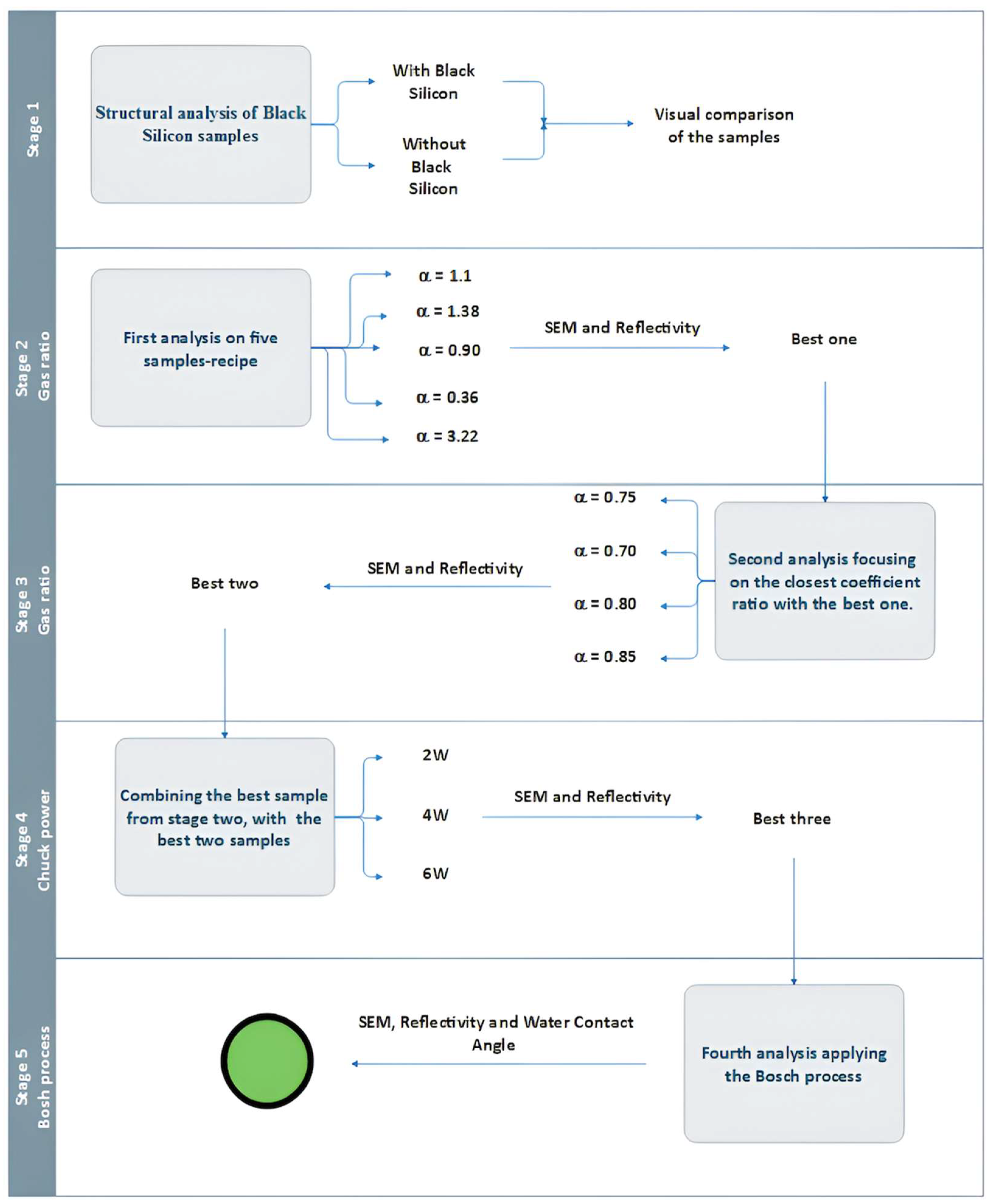
Figure 2.
(a) poor black silicon, (b) descent sample.
Figure 3.
(a) untreated silicon sample, (b) treated black silicon sample, (c) poorly treated sample.
Figure 3.
(a) untreated silicon sample, (b) treated black silicon sample, (c) poorly treated sample.
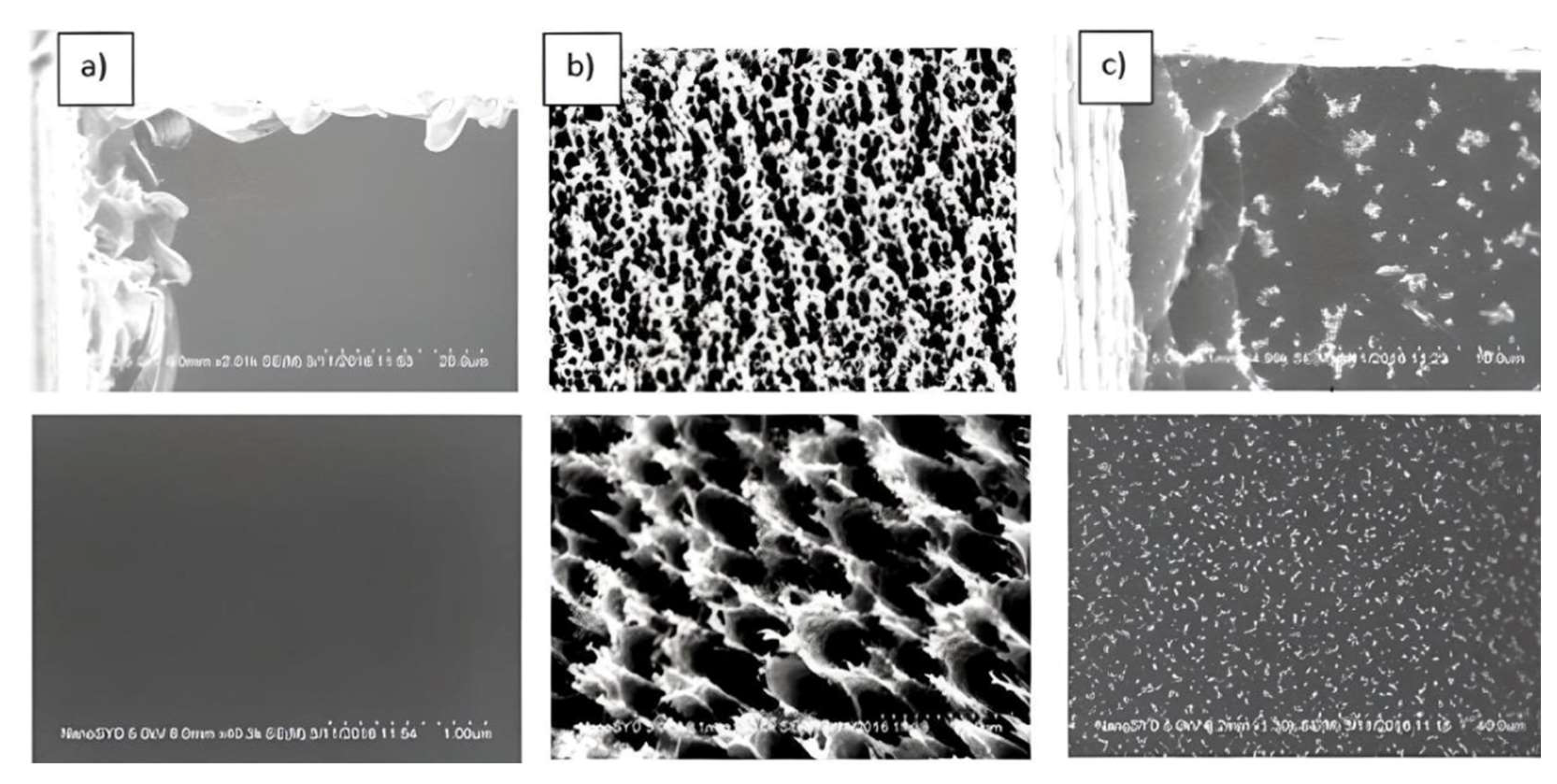
Figure 4.
Top view images of the samples derived from the main recipe.
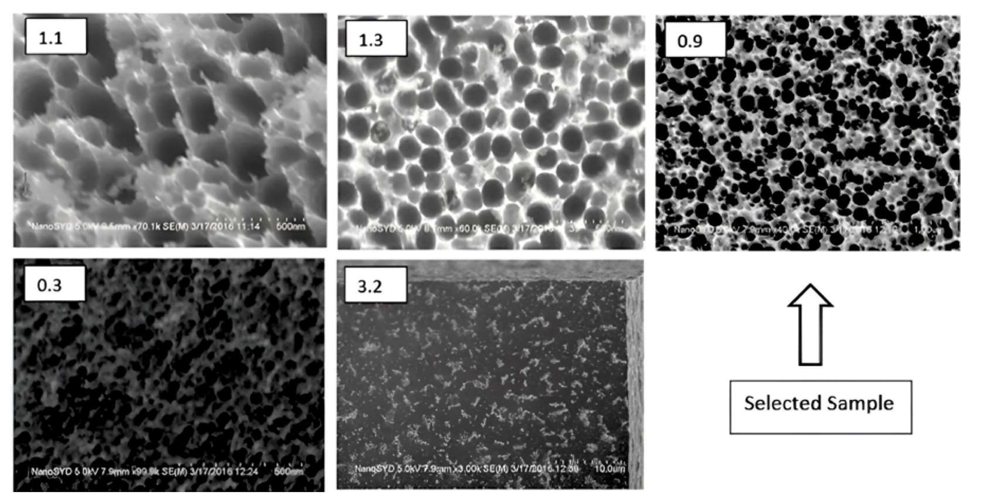
Figure 5.
SEM images from the side view.
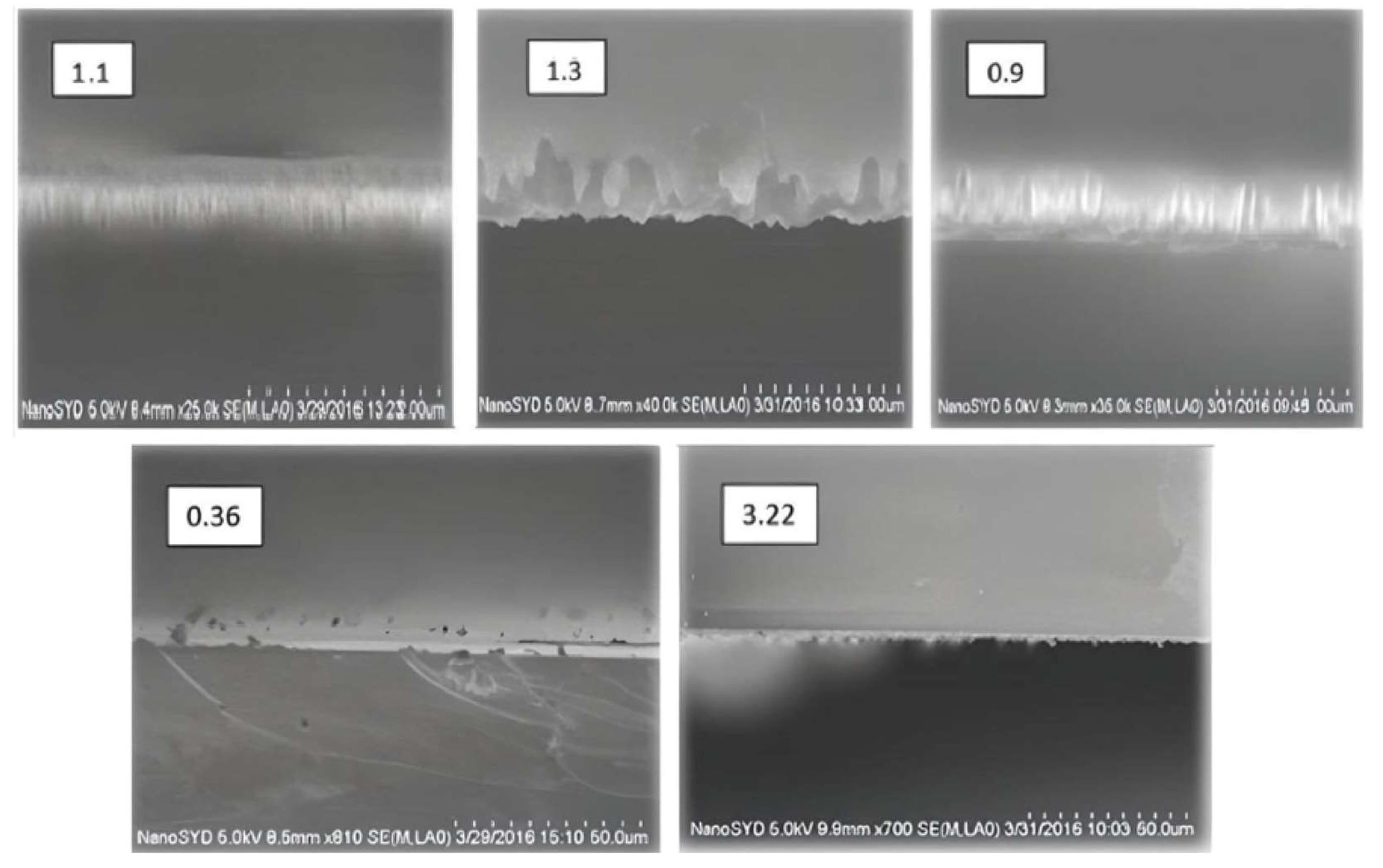
Figure 6.
Geometrical size of the best sample α=0.9.
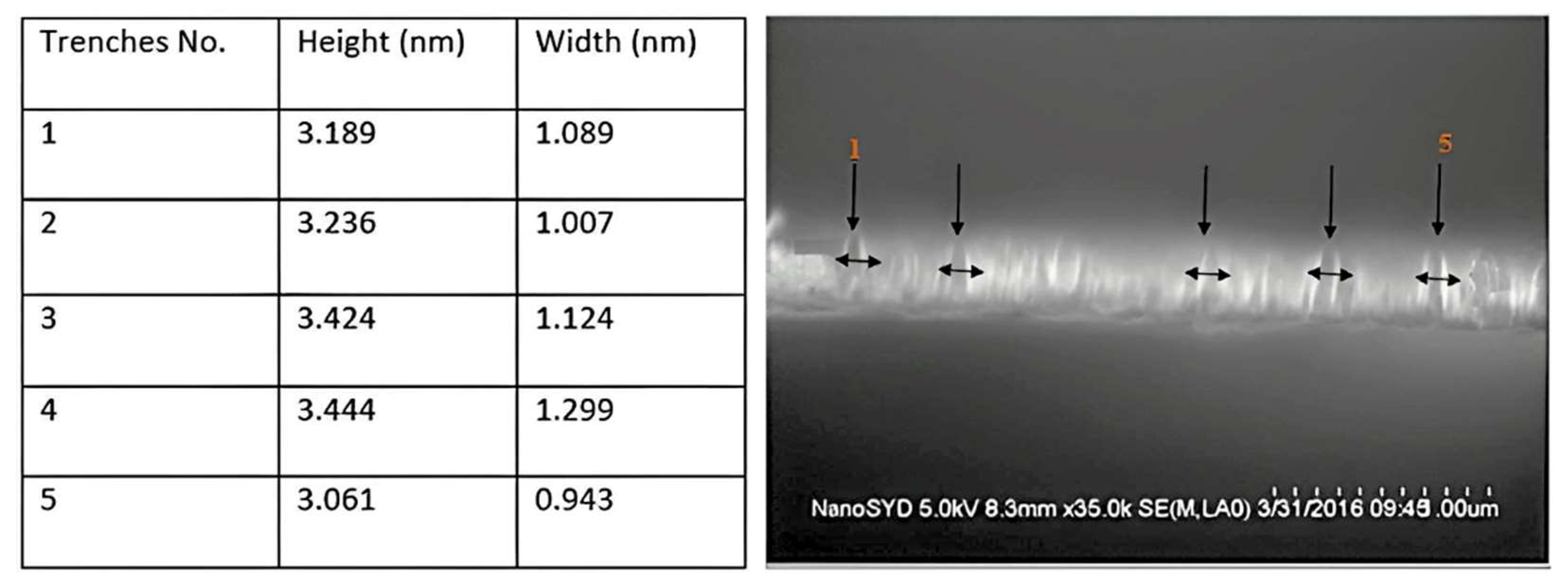
Figure 7.
Reflectivity measurement setup.

Figure 8.
Reflectivity results for the best sample.
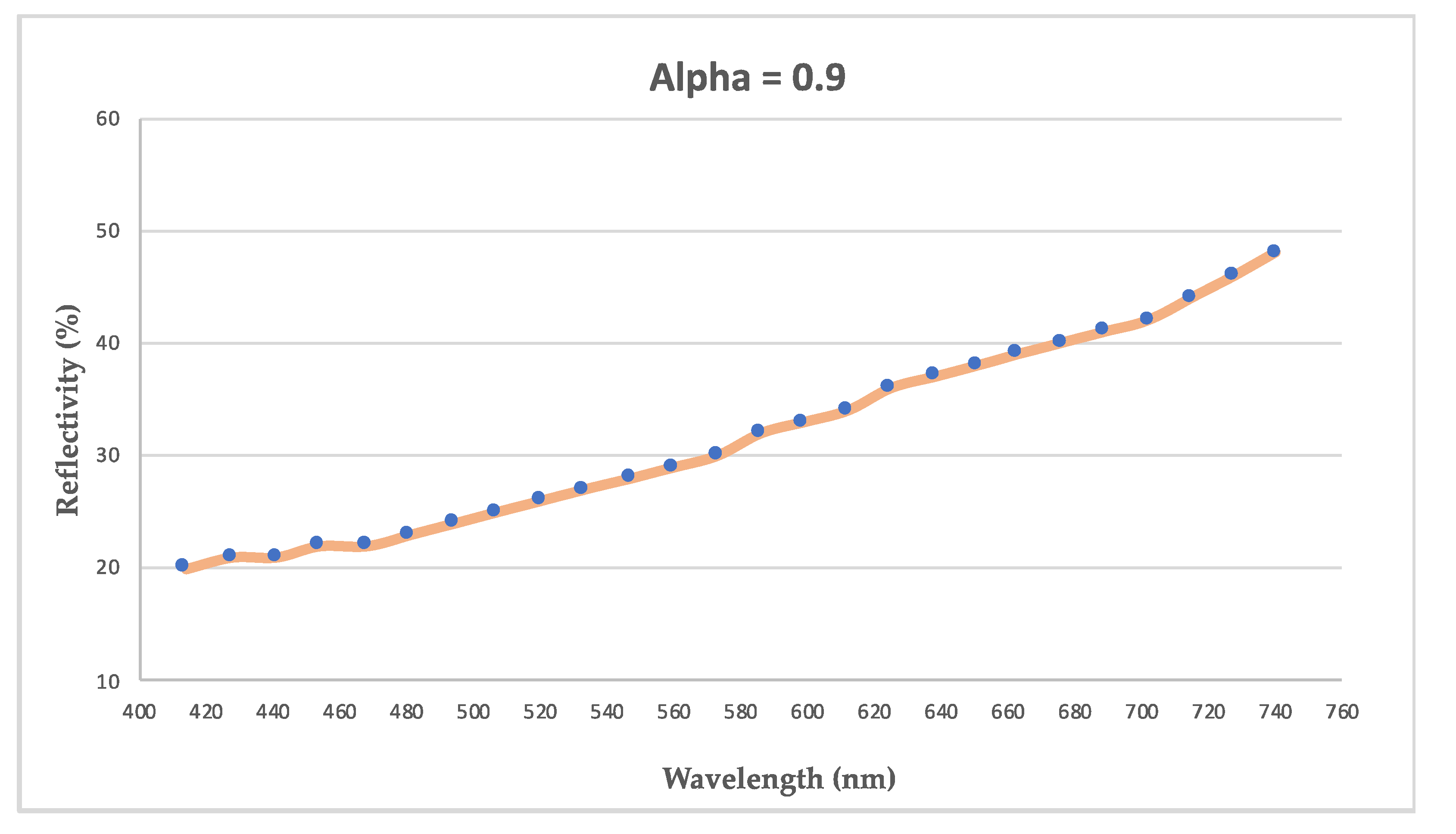
Figure 9.
Top view images for α = 0.7 and 0.75.
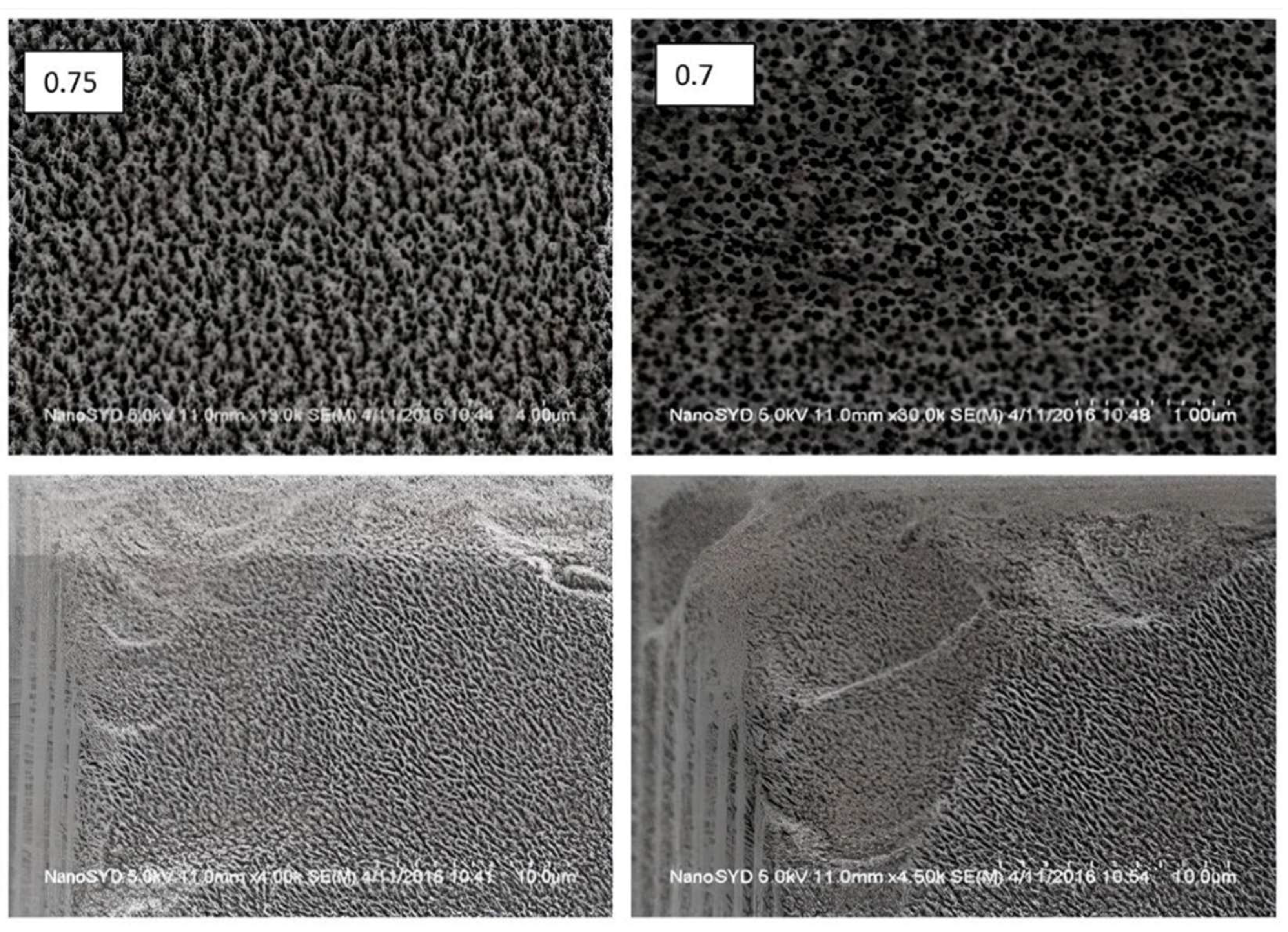
Figure 10.
SEM top view images for α = 0.8 and 0.85.
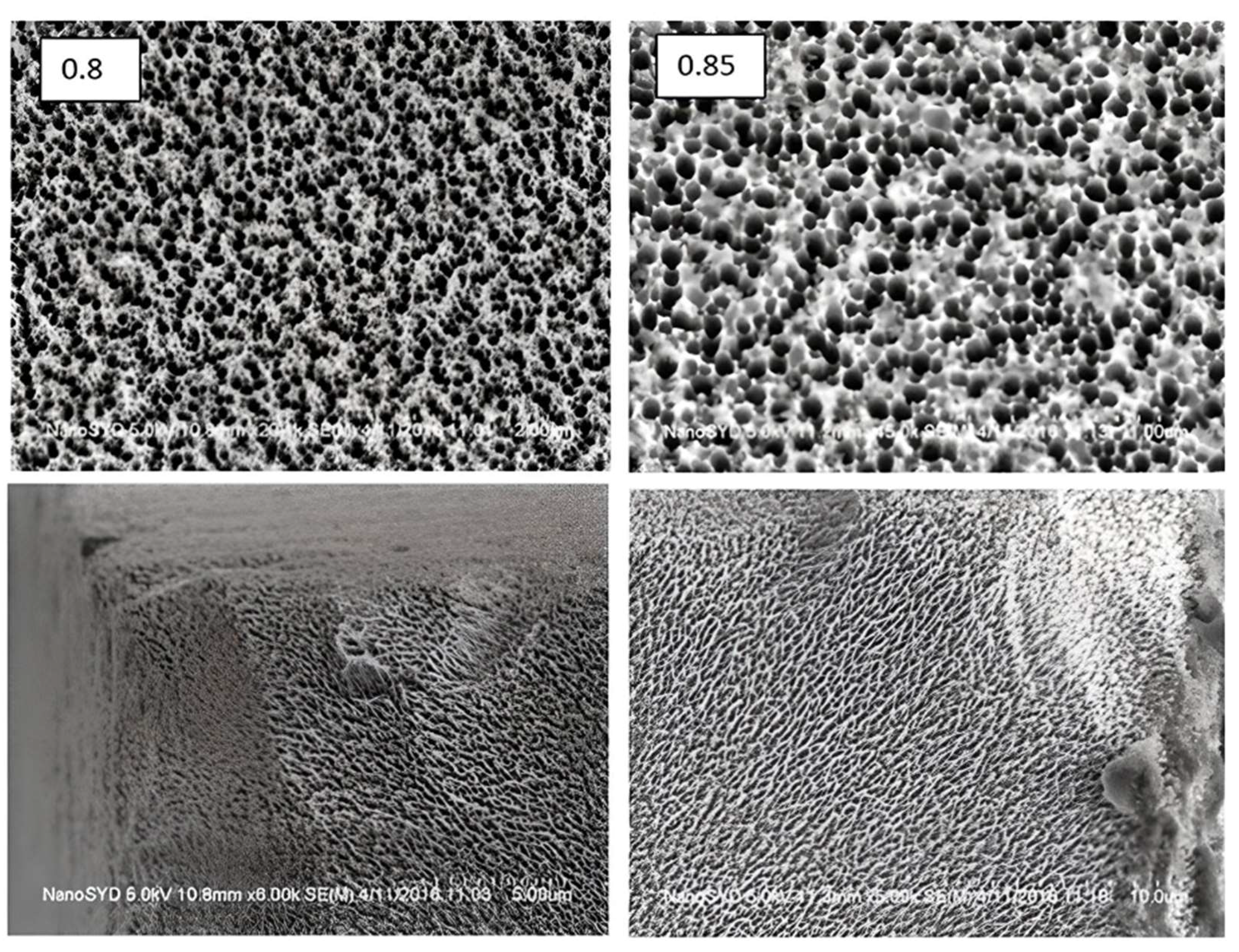
Figure 11.
SEM side view images for α = 0.7 and 0.75.
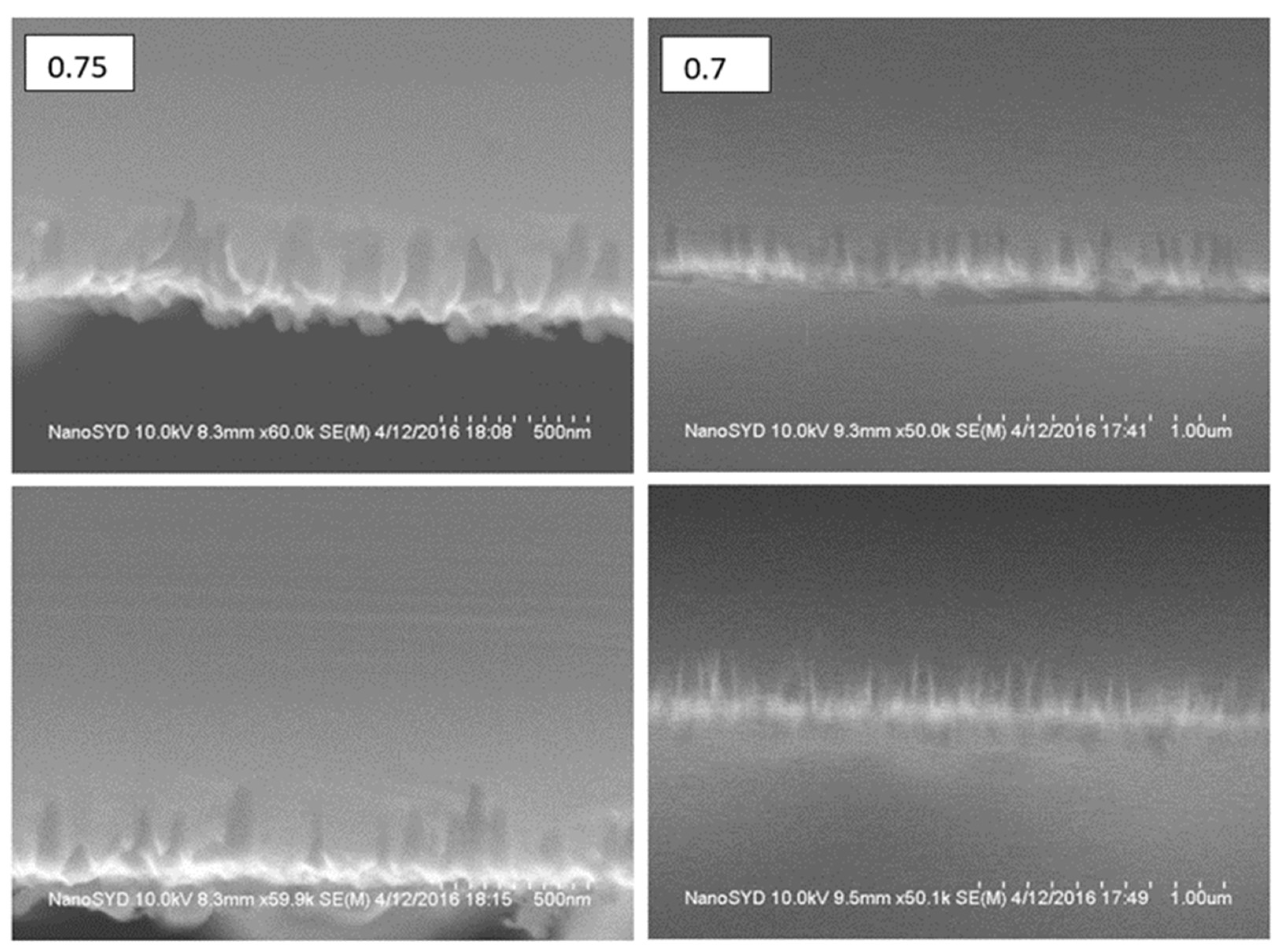
Figure 12.
SEM side view images for α = 0.8 and 0.85.
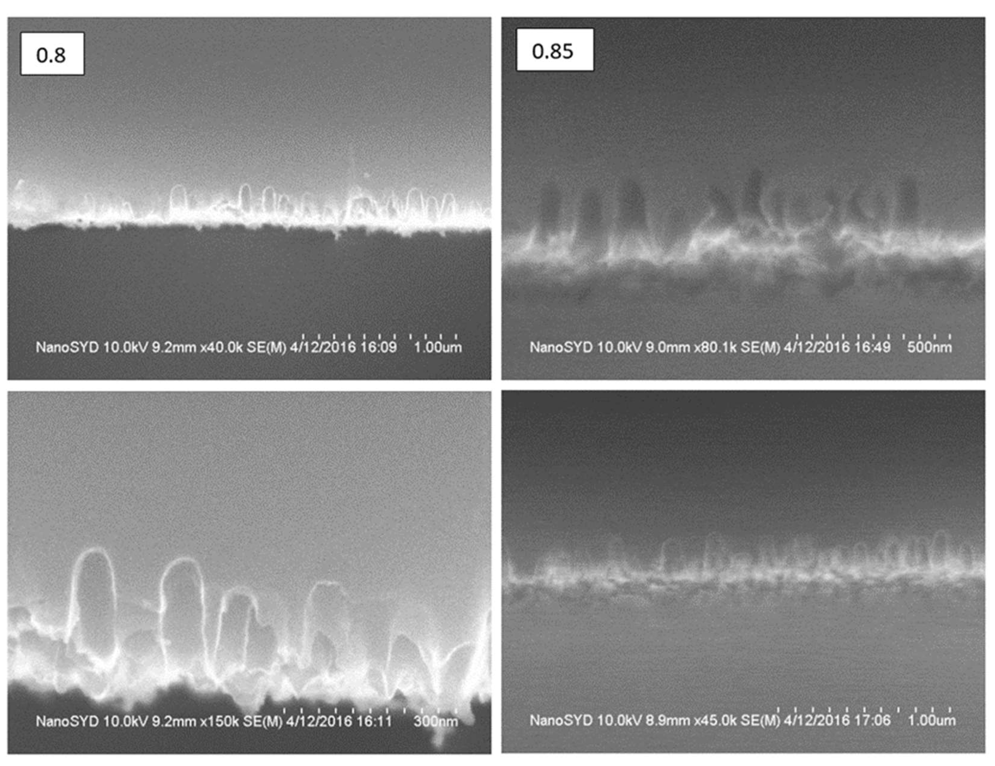
Figure 13.
SEM Reflectivity for α = 0.7, 0.75, 0.8 and 0.85.
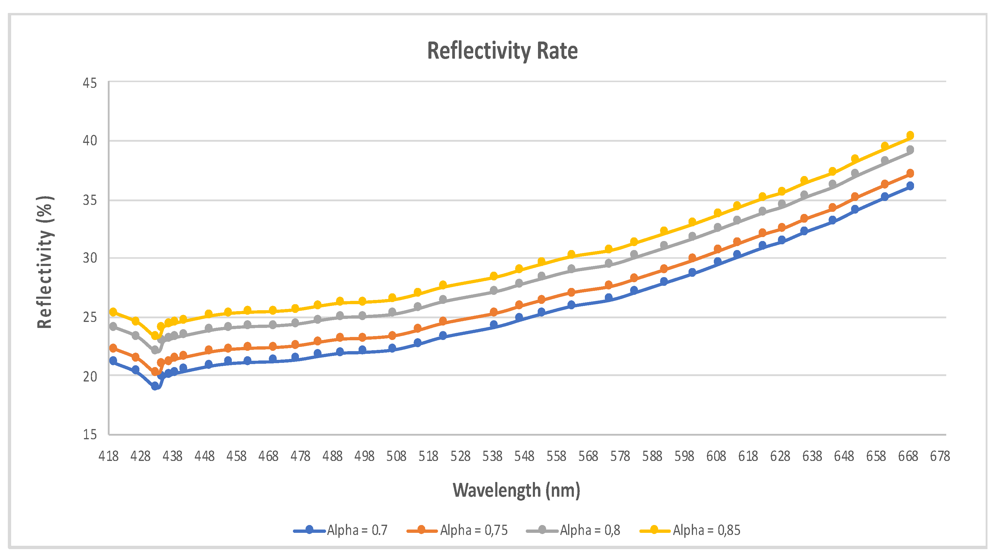
Figure 14.
SEM top view images with different chuck bias power.
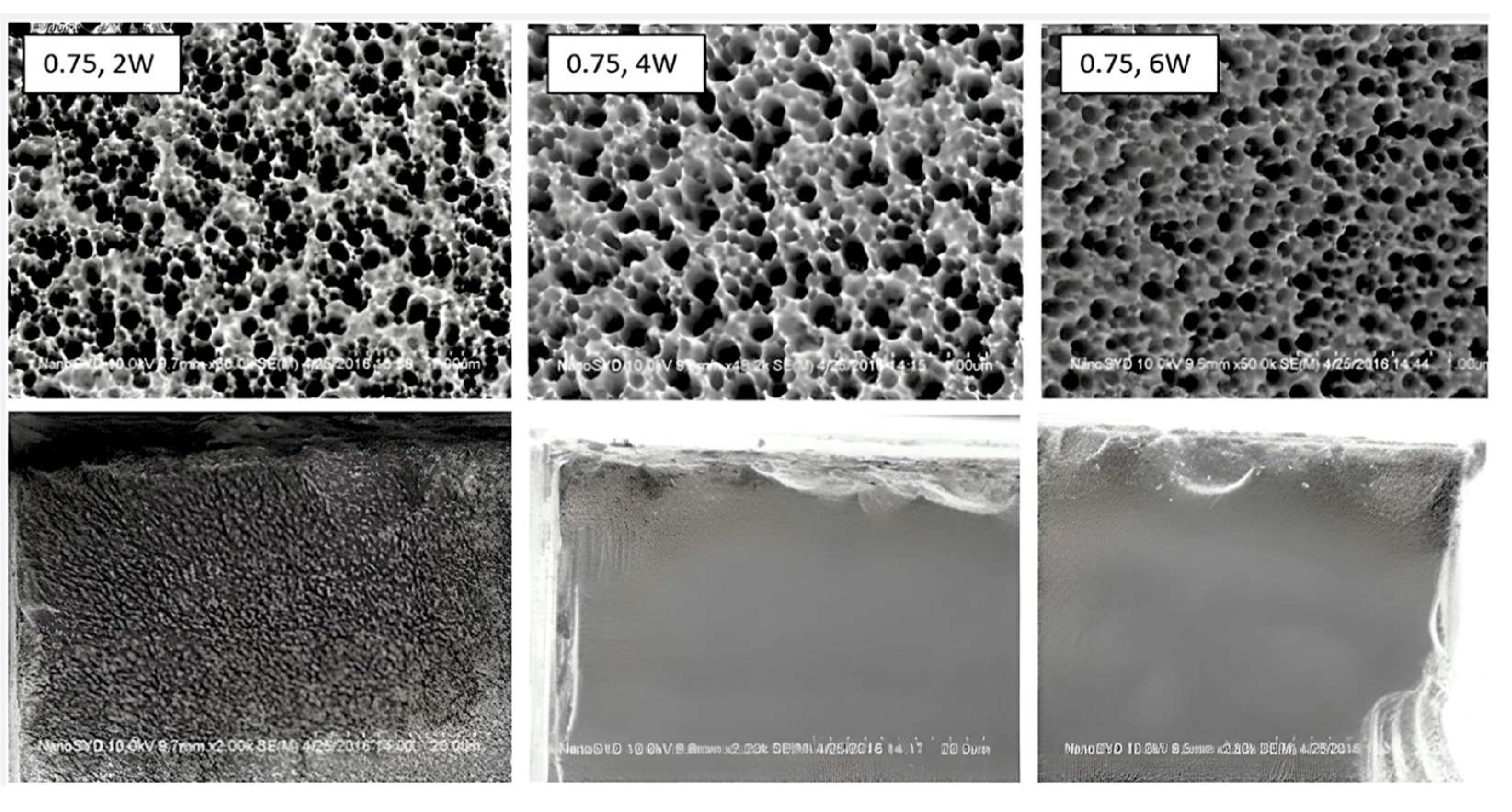
Figure 15.
SEM Top View images.
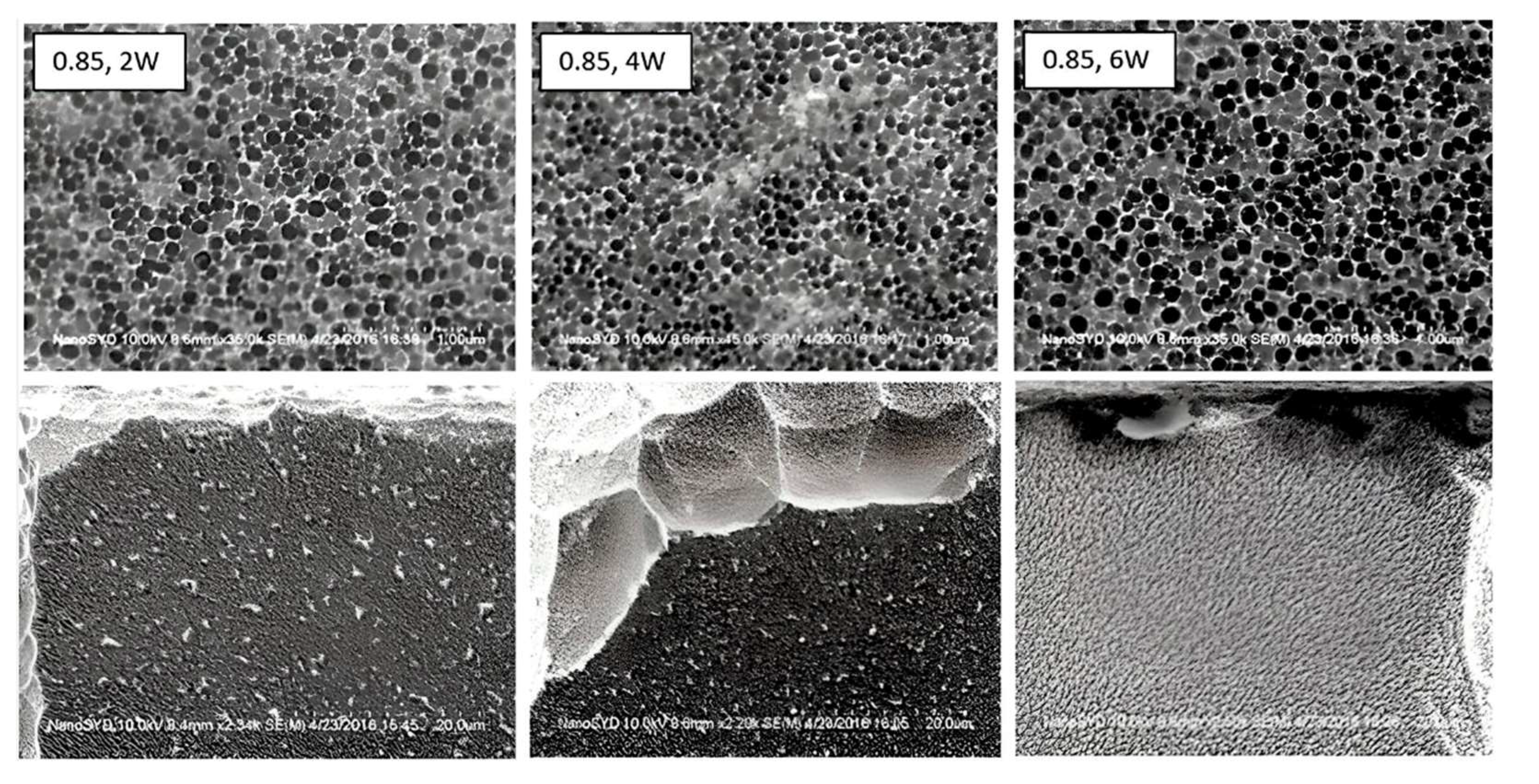
Figure 16.
SEM side view images.
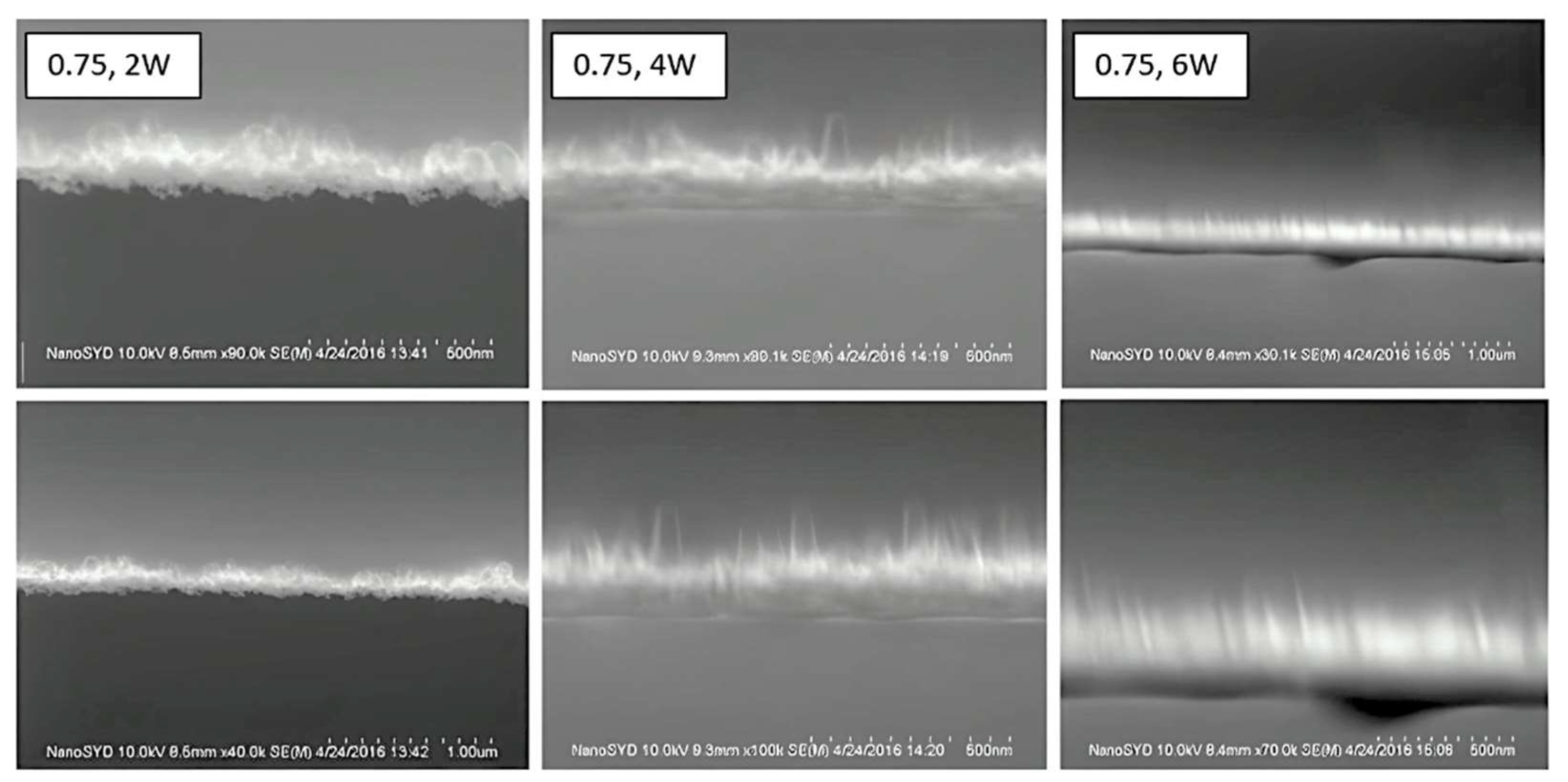
Figure 17.
SEM side view images.
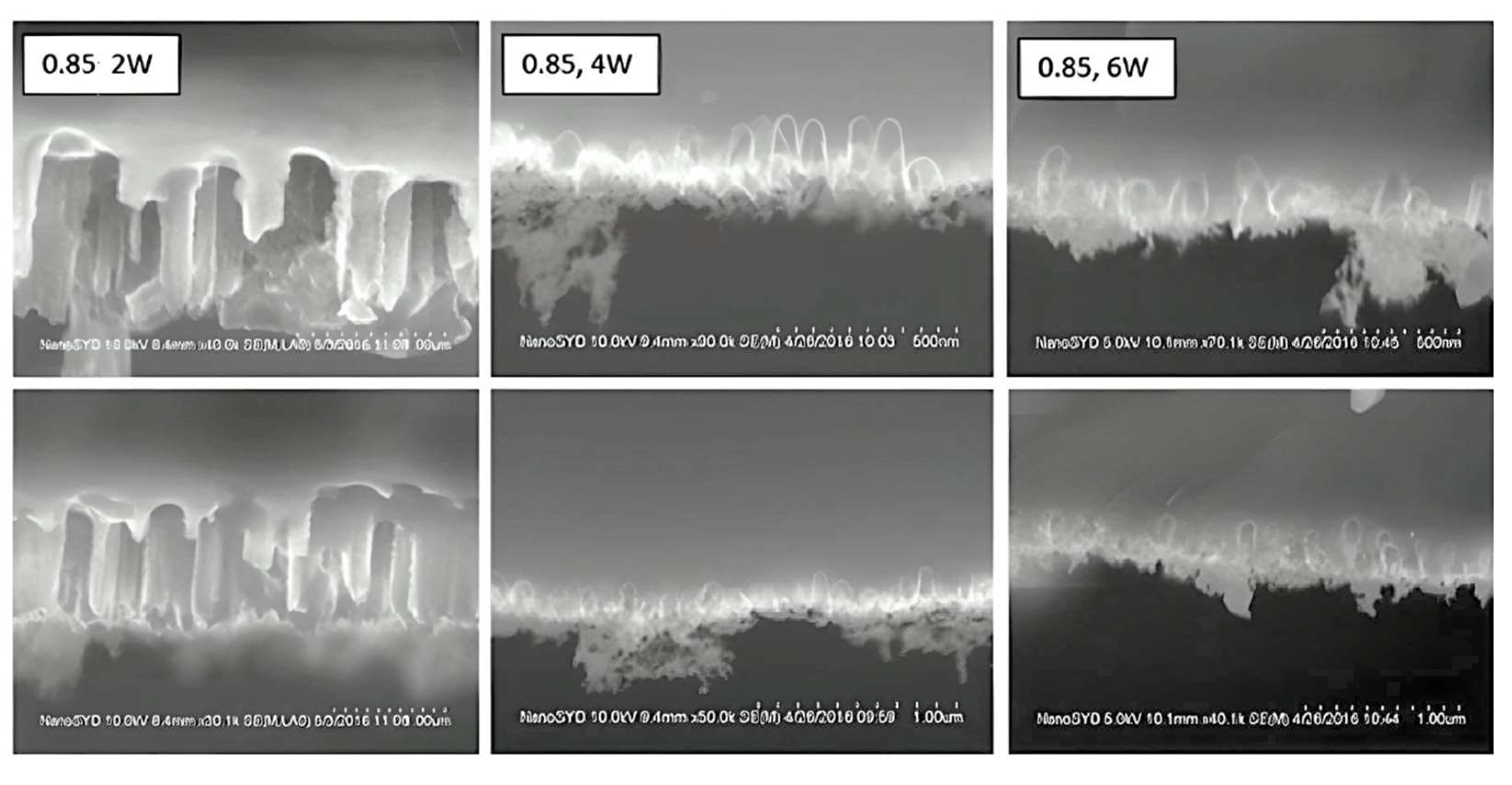
Figure 18.
Reflectivity results across the samples.
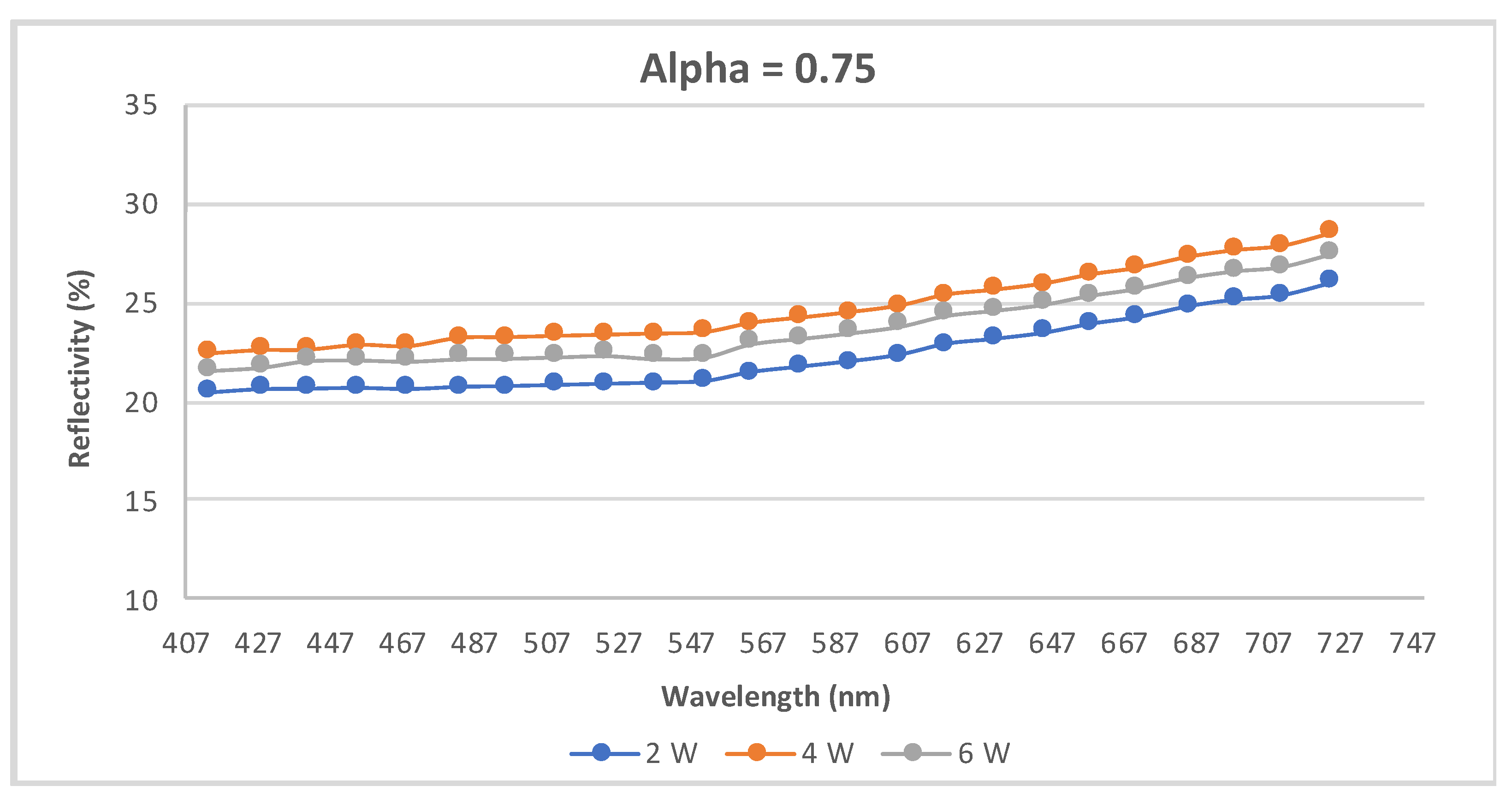
Figure 19.
Reflectivity results across the samples.
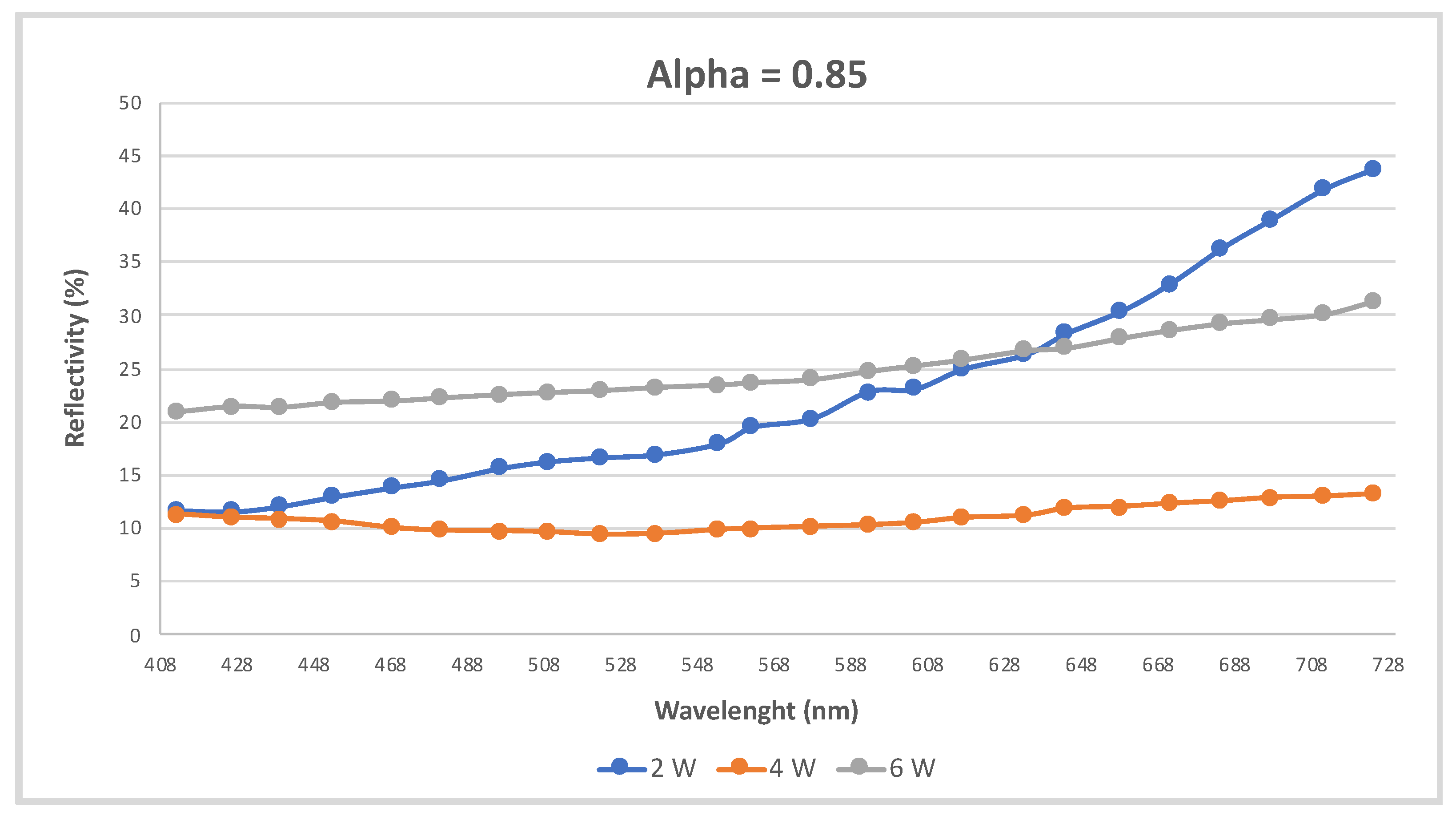
Figure 20.
Bosch process on the selected samples.
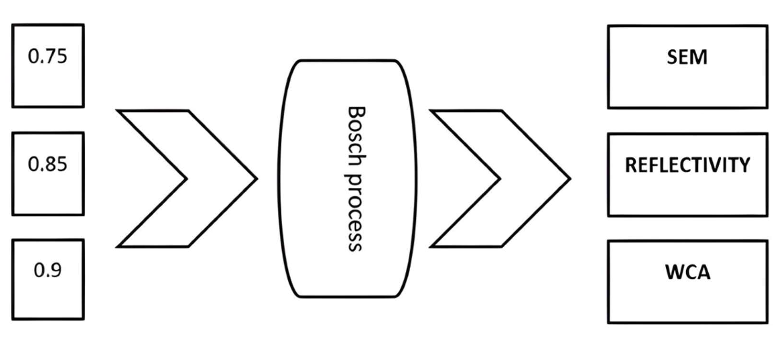
Figure 21.
SEM top view images of the samples treated with Bosch process.
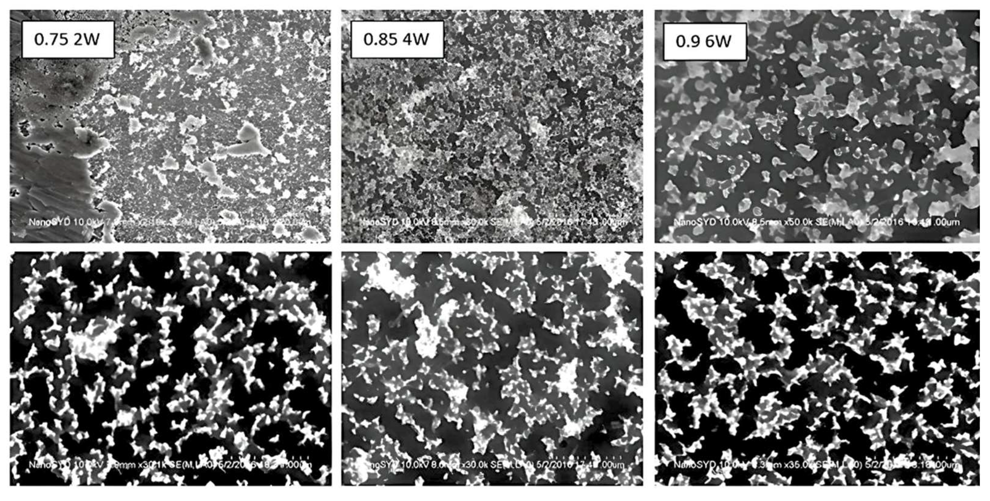
Figure 22.
SEM side view images treated with Bosch.
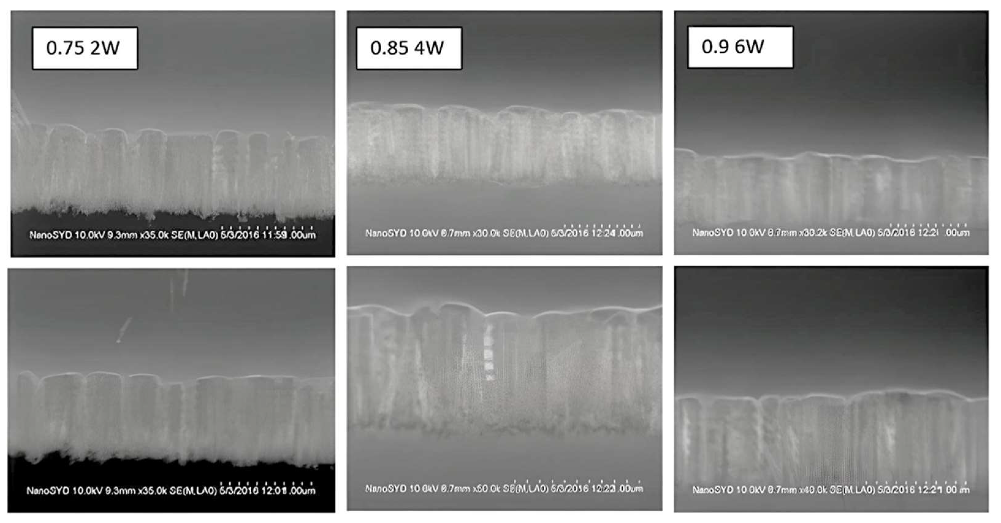
Figure 23.
Reflectivity level for Bosch process best samples.
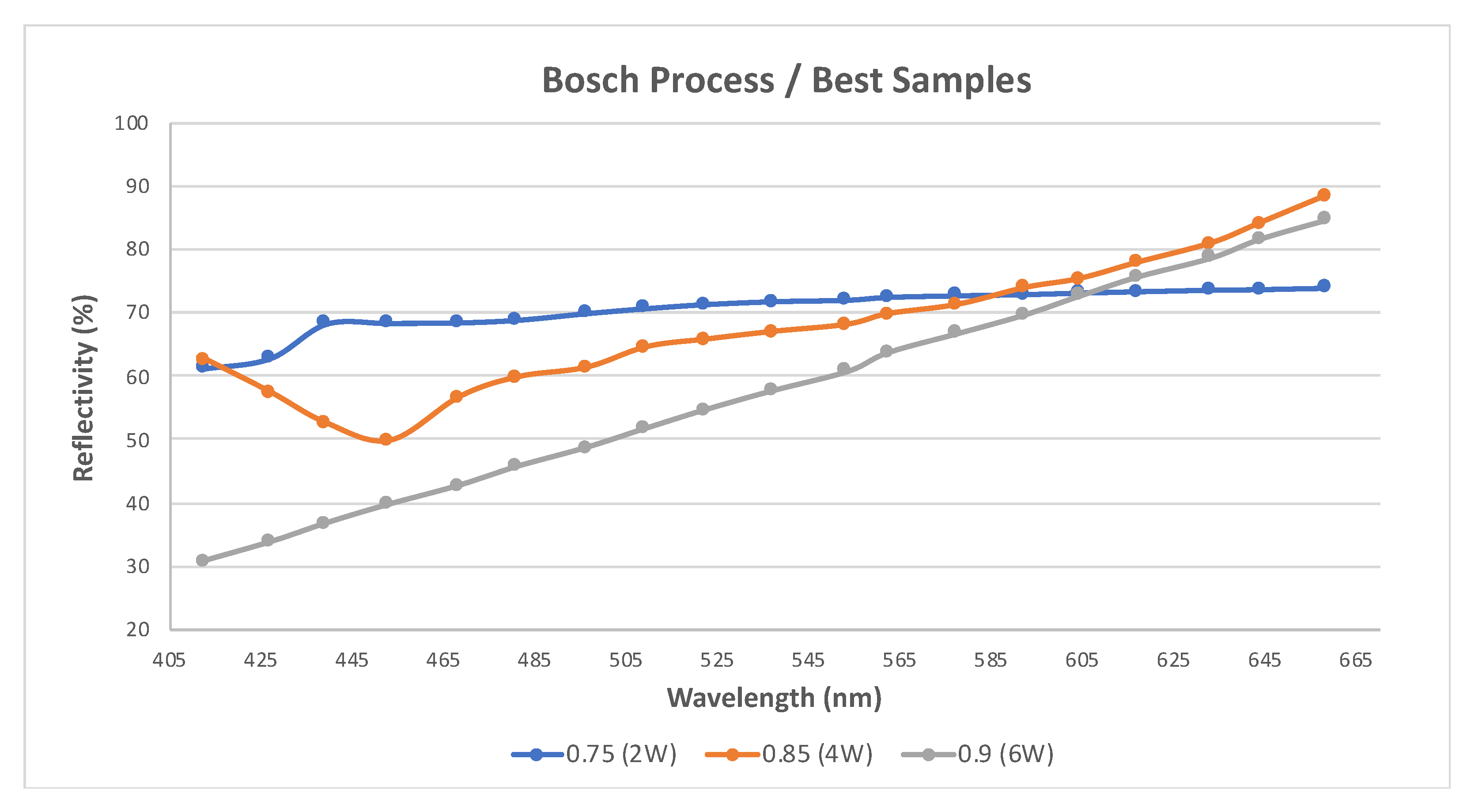
Figure 24.
Hydrophobicity of the samples without Bosch process.
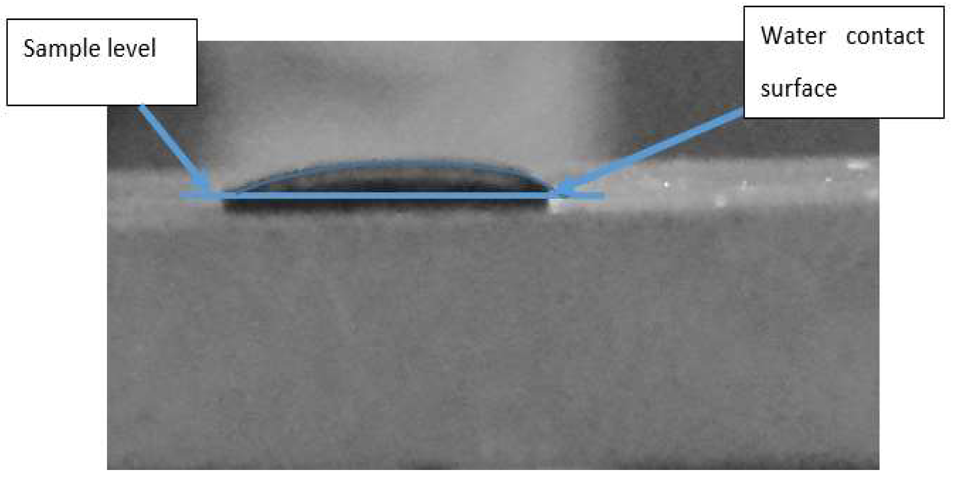
Figure 25.
Hydrophobicity shown from samples treated with Bosch process.
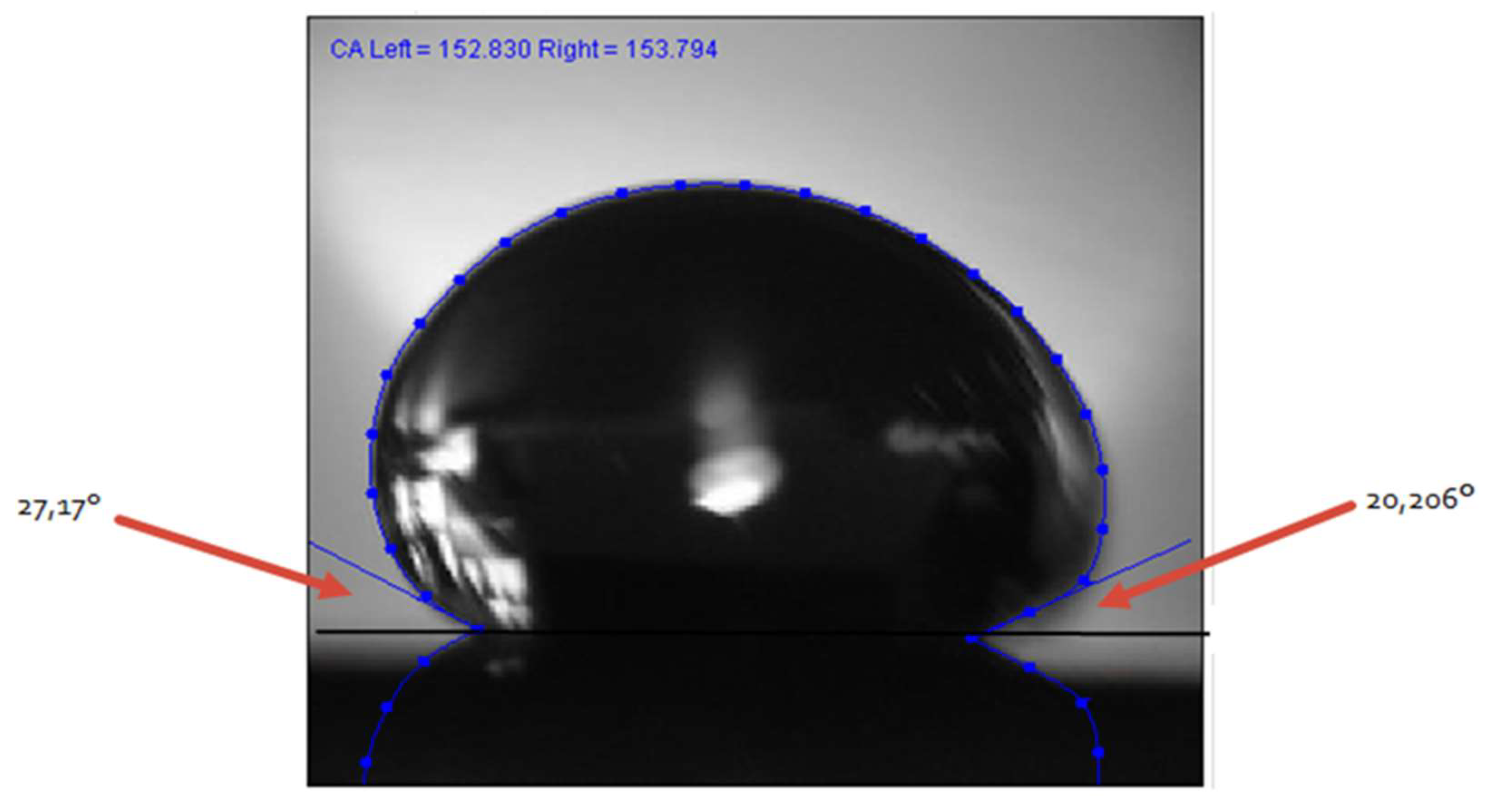
Figure 26.
Lowest reflectivity rate achieved, about 10% for the best sample with α=0.85, chuck bias 4W.
Figure 26.
Lowest reflectivity rate achieved, about 10% for the best sample with α=0.85, chuck bias 4W.
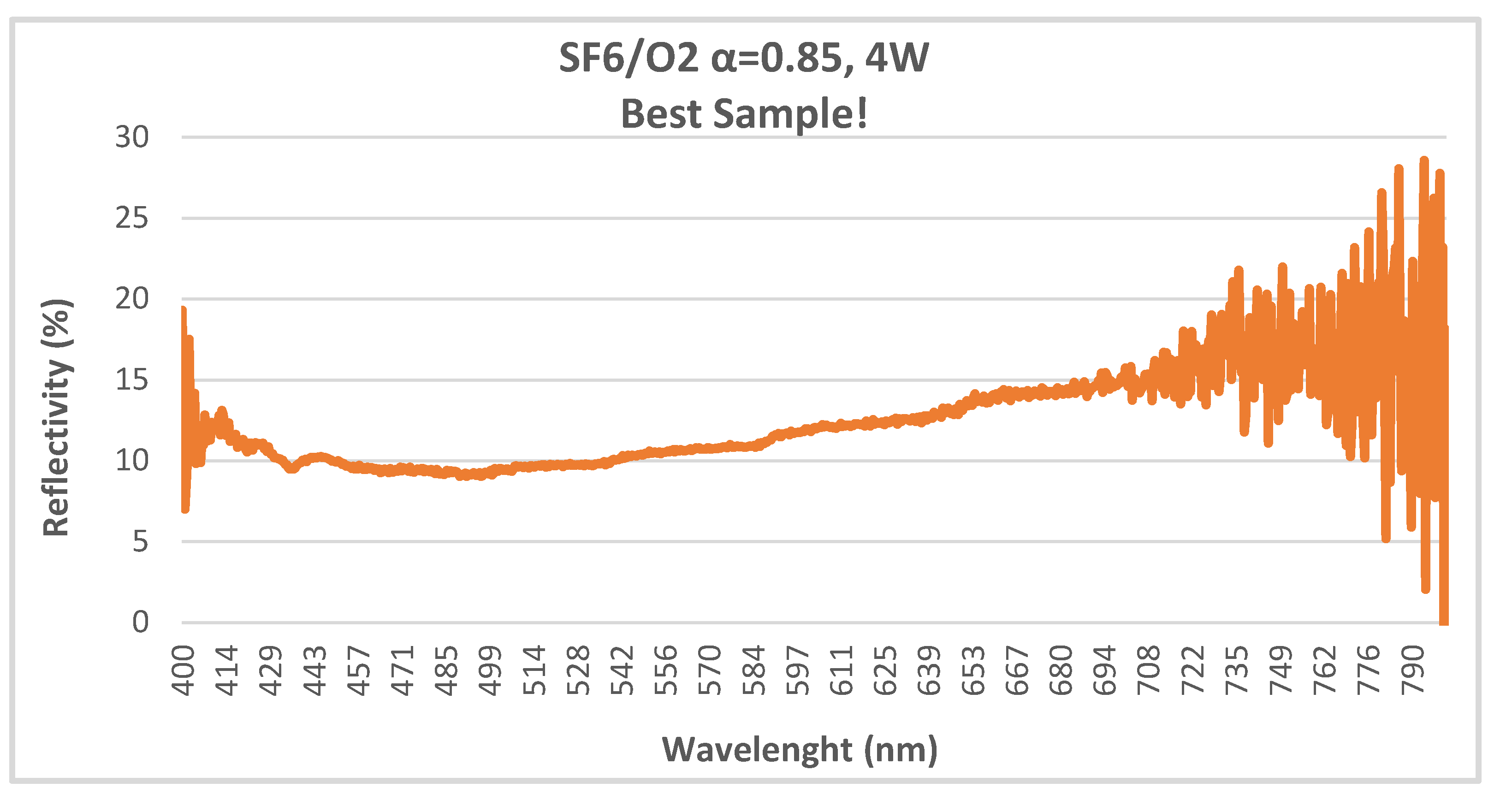

Table 1.
Gas ratios derived from the recipe with gas ratio α=0.9, second stage.
| Alpha SF6/O2 | SF6 | O2 | O2 trend | SF6 trend |
|---|---|---|---|---|
| 1.1 | 100 | 90 | (reference) | (reference) |
| 1.38 | 110 | 80 | -10 | +10 |
| 0.90 | 90 | 100 | +20 | -20 |
| 0.36 | 50 | 140 | +40 | -40 |
| 3.22 | 145 | 45 | -95 | +95 |
Table 2.
Gas ratios for the derived recipes, third stage.
| Ratio SF6/O2 | SF6 | O2 |
Derived from recipes With α 1.1- 0.9 |
| 0.75 | 81.4 | 108.6 | |
| 0.70 | 78.2 | 111.8 | |
| 0.80 | 84.4 | 105.6 | |
| 0.85 | 87.3 | 102.7 |
Table 3.
Table of variables changed.
| Ratio SF6/O2 | SF6 (sccm) | O2 (sccm) | Chuck bias (W) | Derived from recipes 0.75-0.85 |
| 0.75 | 81.4 | 108.6 | 2 | |
| 81.4 | 108.6 | 4 | ||
| 81.4 | 108.6 | 6 | ||
| 0.85 | 87.3 | 102.7 | 2 | |
| 87.3 | 102.7 | 4 | ||
| 87.3 | 102.7 | 6 |
Table 4.
Gas ratios values.
| Ratio SF6/O2 | SF6 (sccm) | O2 (sccm) | Chuck power (W) |
| 0.75 | 81.4 | 108.6 | 2 |
| 0.85 | 87.3 | 102.7 | 4 |
| 0.9 | 100 | 90 | 6 |
Disclaimer/Publisher’s Note: The statements, opinions and data contained in all publications are solely those of the individual author(s) and contributor(s) and not of MDPI and/or the editor(s). MDPI and/or the editor(s) disclaim responsibility for any injury to people or property resulting from any ideas, methods, instructions or products referred to in the content. |
© 2024 by the authors. Licensee MDPI, Basel, Switzerland. This article is an open access article distributed under the terms and conditions of the Creative Commons Attribution (CC BY) license (http://creativecommons.org/licenses/by/4.0/).
Copyright: This open access article is published under a Creative Commons CC BY 4.0 license, which permit the free download, distribution, and reuse, provided that the author and preprint are cited in any reuse.


