Preprint
Review

This version is not peer-reviewed.

Sustainable Manufacturing and Applications of Wide-Bandgap Semiconductors

A peer-reviewed article of this preprint also exists.

Submitted:

23 November 2024

Posted:

25 November 2024

You are already at the latest version

Abstract

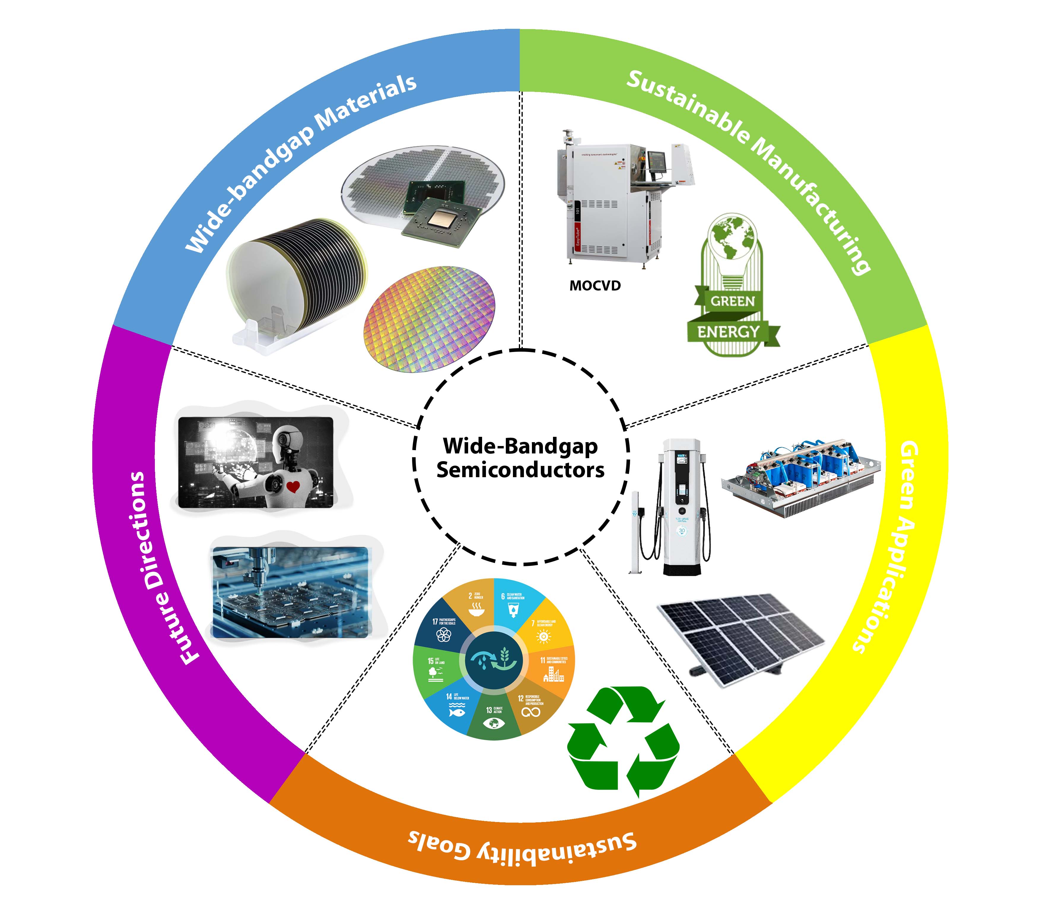
Wide-bandgap (WBG) semiconductors such as silicon carbide (SiC) and gallium nitride (GaN) have become pivotal in high-power, high-frequency, and high-temperature applications. Their superior properties, including higher thermal conductivity, breakdown voltage, and energy efficiency, make them essential for advanced technologies like electric vehicles, renewable energy systems, and 5G infrastructure. However, their production processes are resource-intensive and pose significant environmental challenges. This review explores recent innovations in sustainable WBG manufacturing, focusing on low-energy epitaxial growth techniques, recycling of semiconductor materials, and efforts to reduce toxic byproducts. It also highlights the role of WBG materials in driving next-generation electronic systems and addresses the environmental concerns associated with scaling these materials for widespread use. The potential of Ultrawide-Bandgap (UWBG) materials for even more extreme applications is discussed, underscoring the need for continued innovation in sustainable practices to ensure the long-term viability of WBG technologies.

Keywords: 
;  ;  ;  

1. Introduction

Wide-Bandgap (WBG) semiconductors like silicon carbide (SiC) and gallium nitride (GaN) are gaining recognition as enablers of sustainable technology innovations. Their superior properties in electrical and thermal performances enhance their indispensability in high-power, high-frequency, and high-temperature applications [1,2,3]. As industries engage in efforts to achieve global sustainability goals, WBG semiconductors offer the possibility to significantly improve energy efficiency in industries such as renewable energy, electric vehicles, consumer electronics and telecommunication [3]. However, while WBG materials offer clear advantages in performance and energy conservation, their production processes pose significant environmental challenges creating a paradox between their technological potential and their environmental impact. Addressing this tension is crucial as the world looks toward WBG semiconductors as a means of achieving both technological innovation and sustainability goals.
One of the defining characteristics of WBG semiconductors is their wider bandgap compared to traditional silicon-based semiconductors (Figure 1(a)). Their wider bandgap allows these materials to support higher voltages, higher frequencies, and higher temperatures, without the efficiency losses that are typical in silicon-based devices [4,5]. SiC and GaN semiconductors exhibit higher breakdown field strengths (Figure 1(b)), enhanced electron mobility, and better thermal conductivity than silicon, making them ideal for demanding applications where efficiency and performance under extreme conditions are critical [6]. Consequently, WBG semiconductors are thus better suited to power conversion systems in renewable energy infrastructure, electric vehicles (EVs), and next-generation power grids, where higher power density and greater energy efficiency are paramount [7,8].
The transition from silicon to Wide-Bandgap (WBG) semiconductors particularly Gallium Nitride (GaN) and Silicon Carbide (SiC), represents a significant advancement in power electronics mainly in applications like electric vehicles (EVs) and renewable energy systems. WBG devices possess a number of superior properties: high switching frequencies, reduced conduction losses and compact designs-resulting in enhanced efficiency in power conversion systems. For instance, GaN-based inverters showed peak efficiencies as high as 97.2%, significantly outperforming their traditional silicon solutions [7]. In EVs, the use of WBG semiconductors allows for improved battery utilization, resulting in longer driving ranges and faster charging times [2]. Furthermore, in renewable energy applications, WBG devices contribute to more efficient solar inverters and wind turbine converters, thereby increasing energy yield and minimizing the carbon footprint of power generation [9,10]. This transition allows significant strides in technological performance and contributes to global sustainability by saving energy and reducing greenhouse gas emissions [11].
Despite the enormous advantages coming from WBG semiconductors, the production processes involved are extremely resource and energy-intensive and raise environmental concerns. The production of SiC wafers, for instance, is characterized by high manufacturing energy demands, contributing to a substantial global warming potential (GWP) [12]. Additionally, epitaxial growth techniques, such as chemical vapor deposition (CVD), are required for high-quality WBG wafers to operate at elevated temperatures further increasing energy consumption and greenhouse gas emissions [4,13]. While WBG devices demonstrate superior performance, the environmental impact of their production processes including a higher carbon footprint compared to traditional silicon manufacturing, necessitates a careful evaluation of sustainability practices within the semiconductor industry [12,14]. Moreover, the extraction and processing of raw materials for WBG semiconductors pose ecological risks. SiC production is energy-intensive, contributing to high global warming potential due to the manufacturing energy required for SiC wafers. GaN relies on gallium, often sourced as a byproduct of aluminum and zinc mining which can lead to habitat destruction and pollution in poorly regulated mining regions [6,7,12]. As the demand for WBG semiconductors increases, the pressure on these finite resources will intensify, exacerbating environmental impacts [15]. Furthermore, the supply chain for these materials is geographically concentrated primarily in regions like China (Figure 2), which controls a significant portion of the global supply [16,17]. This concentration creates potential supply bottlenecks and raises concerns about the long-term sustainability of WBG semiconductor production, necessitating a re-evaluation of mining practices and resource management strategies to mitigate ecological damage.
The environmental challenges associated with WBG semiconductors extend beyond raw material extraction and energy consumption during manufacturing. The lifecycle of Wide-Bandgap (WBG) semiconductors indeed presents significant environmental challenges, particularly concerning their end-of-life disposal. The materials used in WBG devices, such as gallium and silicon carbide, are often difficult to recycle, leading to substantial waste generation and resource loss [19]. The improper management of electronic waste (e-waste) exacerbates pollution and poses health risks, as hazardous substances can leach into the environment [20]. The current methodologies of recycling, such as mechanical and hydrometallurgical processes, are losing their economic and technological viability toward the efficient recovery of valuable material from e-waste [19]. Furthermore, the lack of robust regulatory frameworks and public awareness contributes to the challenges of managing e-waste sustainably [21]. Addressing these issues is crucial for minimizing the environmental footprint of WBG semiconductors and promoting sustainable resource management in the face of growing electronic waste concerns.
To reconcile the benefits of Wide-Bandgap (WBG) semiconductors with their environmental impact, significant efforts are being directed toward more environmentally benign production methods and lifecycle management strategies. Research emphasizes the development of energy-efficient manufacturing processes, such as optimizing epitaxial growth techniques to minimize energy consumption during WBG wafer production, which aligns with the broader goal of reducing the carbon footprint in manufacturing [22]. Sourcing of materials has to be sustainable; the semiconductor foundry industry is increasingly focusing on the minimization of hazardous waste and resource efficiency, which can also be applied to WBG materials [14]. More than that, innovations in recycling technologies are being explored to recover rare materials used in WBG production, thereby mitigating the environmental impacts associated with raw material extraction and promoting a circular economy [23]. These universal efforts are turning out to be indispensable in improving the sustainability of WBG semiconductors facing ever-increasing demand for advanced electronic applications [24].
The integration of sustainability practices in the design and production of Wide-Bandgap (WBG) semiconductor devices is crucial for minimizing environmental impacts. Advanced manufacturing techniques, such as chemical vapor deposition (CVD) at lower temperatures and molecular beam epitaxy (MBE), can significantly reduce energy consumption during production, aligning with the semiconductor industry's goal to lower greenhouse gas emissions [22]. Adopting a circular economy approach by focusing on material efficiency and waste reduction can also enhance sustainability in semiconductor manufacturing. Extending the lifespan of WBG devices is another vital strategy, as it reduces the frequency of replacements and the associated electronic waste [23,25].
The semiconductor industry can enhance its operational efficiency and sustainability by implementing various green supply chain management (GSCM) practices. For instance, adopting advanced technologies such as telematics and data analytics can optimize transportation routes, thereby reducing fuel consumption and emissions during distribution processes [26]. Fostering collaboration with suppliers and logistics providers can facilitate the sharing of best practices and joint initiatives, which is crucial for effective GSCM implementation [26]. Also, integrating sustainability into supply chain strategies can improve brand reputation and customer loyalty while achieving cost savings [27]. The semiconductor sector can also benefit from establishing a structured green supply chain framework, similar to Lenovo's model, which emphasizes cooperation among supply chain partners to enhance sustainability and reduce governance costs [28]. By addressing technological risks and complexities through these practices, the industry can demonstrate a commitment to responsible production and consumption [29,30].
Despite these sustainability initiatives, several challenges are persistent in the manufacturing and life-cycle management of WBG semiconductors. One of the key hurdles is the high cost associated with the production of WBG materials, particularly in comparison to traditional silicon-based semiconductors. The energy-intensive process in the case of WBG contributes to the higher costs, which may be a barrier to penetration into cost-sensitive industrial applications [14]. To address these challenges, the semiconductor industry must focus on innovations in manufacturing techniques and achieving economies of scale, as highlighted in the research on green supply chain adoption [29]. Integrating sustainability at product development can further increase the capability of the industry to go through cost reduction with improved environmental performance [31]. The need for sustainable engineering solutions is underscored by the broader challenges of balancing economic viability with environmental impact, as outlined in the Sustainable Development Goals [32]. Overcoming these hurdles is essential for the global viability of WBG semiconductors in sustainable technologies.
Another challenge lies in the need for a more robust infrastructure to support the recycling and recovery of WBG materials. Wider utilization of WBG semiconductors requires better recycling technologies capable of reclaiming expensive materials from end-of-life devices. The automotive sector for instance, is increasingly focusing on circular economy principles, emphasizing the recovery of valuable materials from electronic components, including WBG devices, through innovative decision-making frameworks that enhance sustainability [23]. The recycling of lithium-ion batteries (LIBs), which may incorporate WBG materials, is gaining attention due to regulatory pressures and the need for efficient resource management [33]. The challenges of developing effective recycling technologies for WBG materials highlight the importance of collaboration among industry, government, and academia to create regulatory frameworks that incentivize recycling efforts [34]. The transition towards a circular economy requires comprehensive strategies that address the entire lifecycle of materials, ensuring that valuable resources are reclaimed and reused effectively [35,36].
This review provides an in-depth exploration of the innovations, sustainability practices, challenges, and future prospects of Wide-Bandgap (WBG) semiconductors. The first section analyzes recent advancements in WBG technologies, with a focus on their applications in high-power, high-efficiency industries, such as renewable energy systems and electric vehicles, where they are revolutionizing performance and efficiency. The second section delves into current sustainability initiatives aimed at mitigating the environmental impact of WBG semiconductor production, such as improving energy efficiency, minimizing material waste, and developing advanced recycling techniques. The third section addresses the specific challenges associated with WBG semiconductor production, ranging from raw material extraction to lifecycle management, and evaluates the industry's response to these environmental concerns. Finally, the review looks ahead to the future of WBG semiconductors, discussing their potential to drive sustainable technological innovation and outlining the strategic steps required to align their development with broader sustainability goals.

2. Semiconductor Fundamentals and Historical Development

2.1. Introduction to Semiconductors

Semiconductors are essential materials characterized by their electrical conductivity, which lies between that of conductors and insulators, making them vital for controlling electric current in electronic devices [37]. They are classified into intrinsic semiconductors, which are pure, and extrinsic semiconductors, which are doped with impurities to enhance conductivity [38]. Among the semiconductors, silicon is used extensively due to its high-temperature stability and effective doping capabilities, allowing for the creation of both p-type and n-type semiconductors [38,39]. This ability to be doped and integrated into complex circuits has been foundational for modern electronics, supporting the development of a wide range of devices, from computers to telecommunications systems [40]. The dominance of silicon underscores its central role in advancing various technological applications, highlighting its significance in the evolution of electronic technology [39,40].

2.2. The Shift to Wide-Bandgap (WBG) Semiconductors

The increasing demand for more efficient, reliable, and high-performance electronic systems has driven a transition from traditional silicon-based semiconductors to Wide-Bandgap (WBG) technologies. Wide-bandgap (WBG) semiconductors like Silicon Carbide (SiC) and Gallium Nitride (GaN) outperform Silicon (Si) by offering significantly larger bandgaps - around 3.3 eV for Silicon and 3.4 eV for GaN (Table 1, Figure 3). This enables WBG devices to operate at much higher voltages, temperatures, and frequencies while reducing energy losses and minimizing thermal degradation [41].
As industries such as electric vehicles, renewable energy systems, and aerospace demand greater efficiency and power density, the limitations of silicon devices—especially in terms of temperature tolerance and frequency—have become more apparent. SiC devices, for instance, maintain functionality at temperatures exceeding 200°C, while GaN excels in high-frequency applications, offering superior performance in power conversion and RF applications [5,41]. The higher thermal conductivity and breakdown voltages of WBG materials also ensure greater reliability in extreme conditions, reducing the need for additional cooling systems and enhancing long-term durability [41,42].
This transition to WBG technology represents a pivotal advancement in semiconductor design, fostering the development of more efficient and robust electronic systems. This transition is crucial for meeting the evolving needs of green technologies, electrified transportation, and next-generation power electronics [5,43].

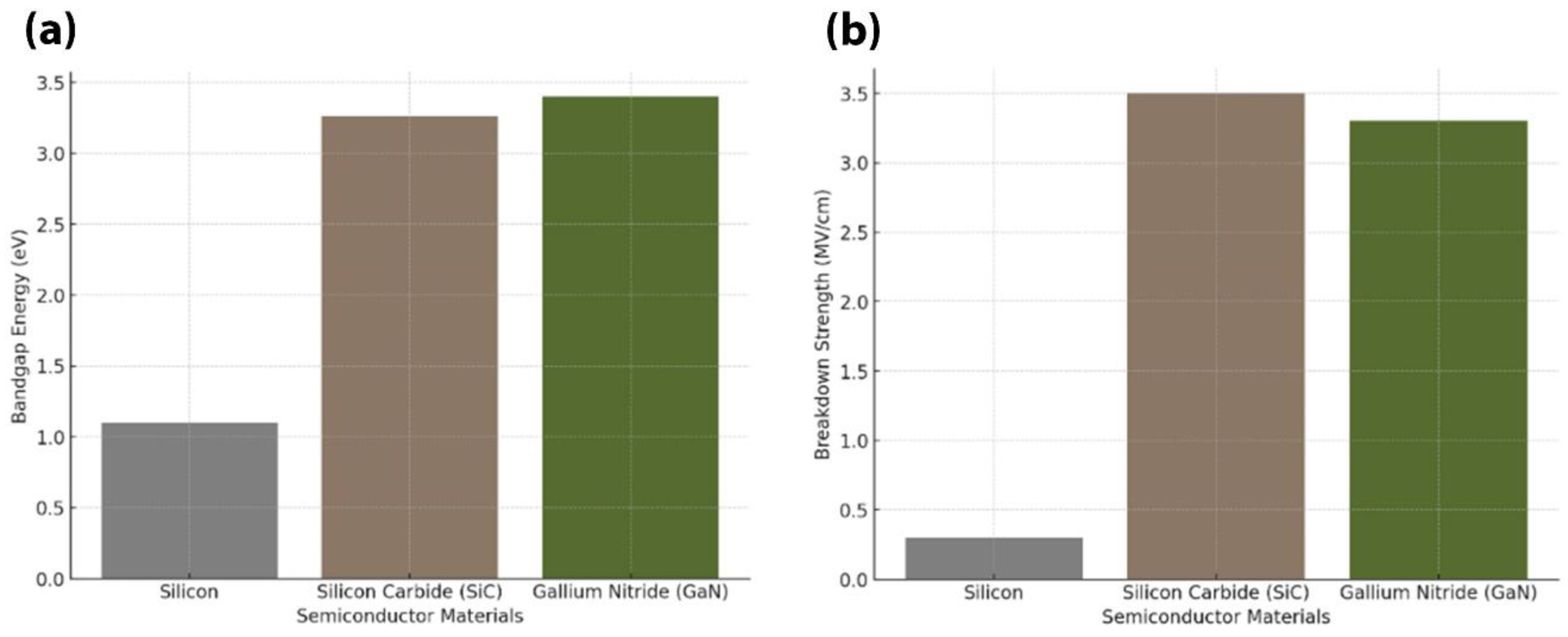
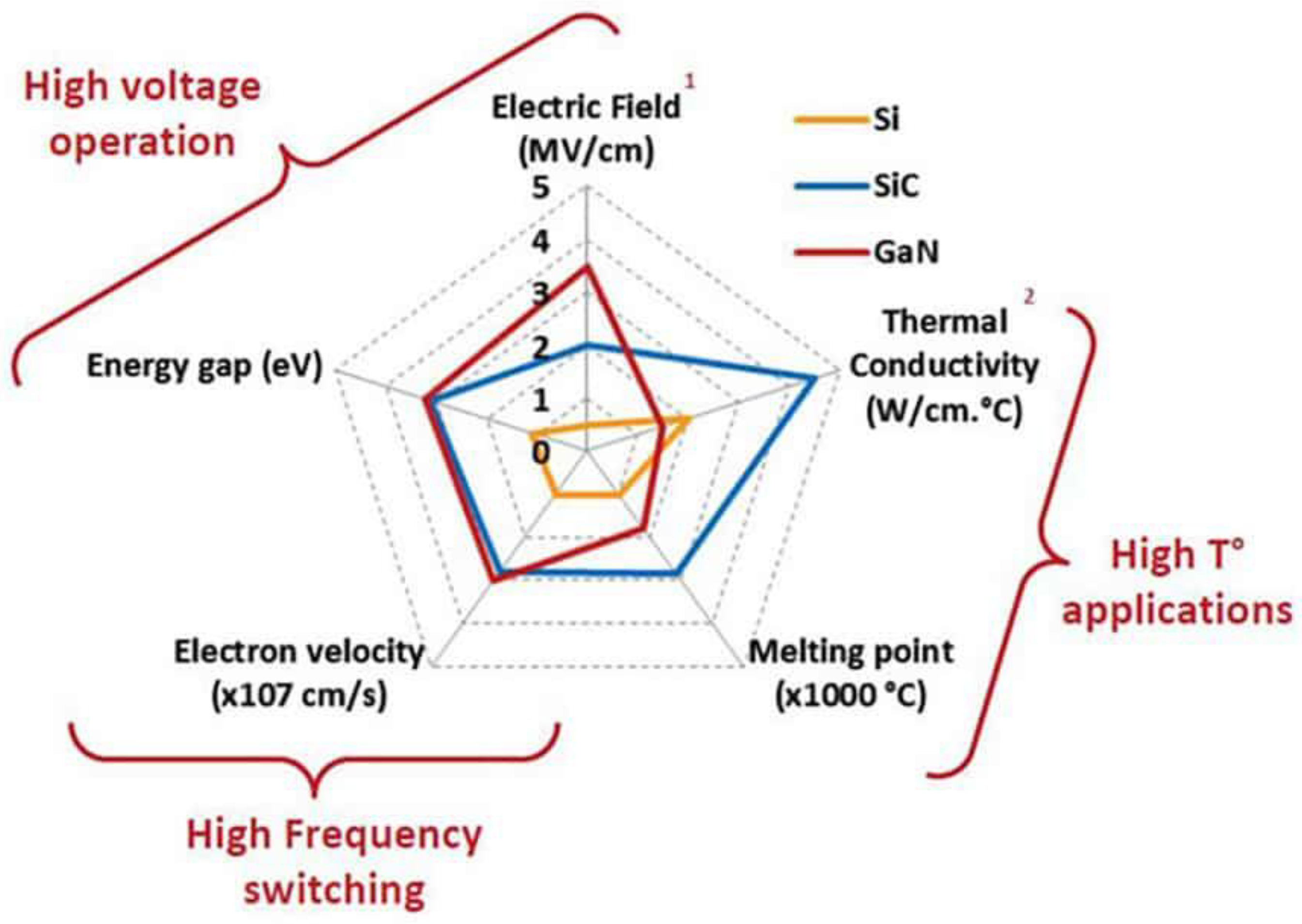
2.3. Fundamental Properties of Wide-Bandgap (WBG) Semiconductors

With their inherent properties, WBG devices can function effectively at temperatures up to 300°C, far exceeding the 150°C limit of traditional silicon devices [2,41]. The superior material properties of WBG semiconductors, including high thermal conductivity and reduced conduction losses, enable them to be appropriate for demanding applications in electric vehicles, renewable energy systems, and aerospace.[7,9]. Their ability to switch at high frequencies while maintaining efficiency enhances the performance of power converters, which is crucial for the evolving needs of electrified transportation and green technologies [1,2].
Silicon carbide (SiC) exhibits a thermal conductivity of approximately 3.7 W/cmK, which is significantly higher than silicon's 1.5 W/cmK (Table 1, Figure 3), making SiC particularly advantageous for high-temperature applications such as electric vehicle powertrains due to its effective heat dissipation capabilities [41]. In contrast, gallium nitride (GaN) has a lower thermal conductivity of about 1.3 W/cmK; however, its superior electron mobility (Table 1) allows for enhanced efficiency in high-frequency switching applications, as utilized in 5G networks and radar systems [44]. The thermal management of GaN-based devices is critical, as self-heating effects can lead to performance degradation [44] Furthermore, the thermal conductivity of GaN can be influenced by structural properties, impurities, and layer thickness, which are essential considerations for optimizing device performance [45,46]. Thus, while SiC excels in thermal conductivity, GaN's high electron mobility makes it a strong candidate for specific high-frequency applications.
Table 1. Physical properties of Silicon (Si), Silicon Carbide (SiC) and Gallium Nitride (GaN) [47].
ELECTRICAL PROPERTY SI 4H-SIC GAN
BANDGAP ENERGY (EV) 1.1 3.26 3.4
THERMAL CONDUCTION (W/CM.K) 1.5 3.7 1.3
ELECTRON MOBILITY (CM2/V.S) 1300 900 900 - 2000
SATURATION DRIFT VELOCITY 1 x 10⁷ 2 x 10⁷ 2.5 x 10⁷
Silicon Carbide (SiC) and Gallium Nitride (GaN) significantly outperform traditional silicon in terms of breakdown voltage, with SiC capable of handling up to 1,700 V and GaN around 650 V, compared to silicon's maximum of about 400 V [41]. This enhanced voltage handling allows for more compact designs in power electronics, as fewer components are required to manage the same power load, thereby improving device efficiency and reliability [7]. High thermal conductivity and fast electron mobility are other superior material properties of WBG semiconductors contributing to their effectiveness in high-power applications. [2,9]. WBG devices are increasingly finding their applications in solar inverters, electric grids, and other applications that demand both compactness and high performance. This is essential for the evolving landscape of power electronics [11].
Gallium Nitride (GaN) exhibits remarkable efficiency in high-frequency applications due to their superior electron mobility of 2,000 cm²/Vs (Table 1), which facilitates faster-switching speeds and minimizes energy losses during power conversion [2]. This characteristic is especially beneficial in renewable energy systems, where efficient power conversion is essential for maximizing energy output [9]. GaN's capability to operate at elevated frequencies allows for the integration of smaller passive components, resulting in lighter and more compact power electronic devices [7,48]. The reduced size of these components not only enhances the overall system efficiency but also contributes to the development of more space-efficient designs, which is critical in applications such as electric vehicles and renewable energy inverters [49]. Overall, the advantages of GaN in high-frequency applications underscore its pivotal role in advancing modern power electronics.

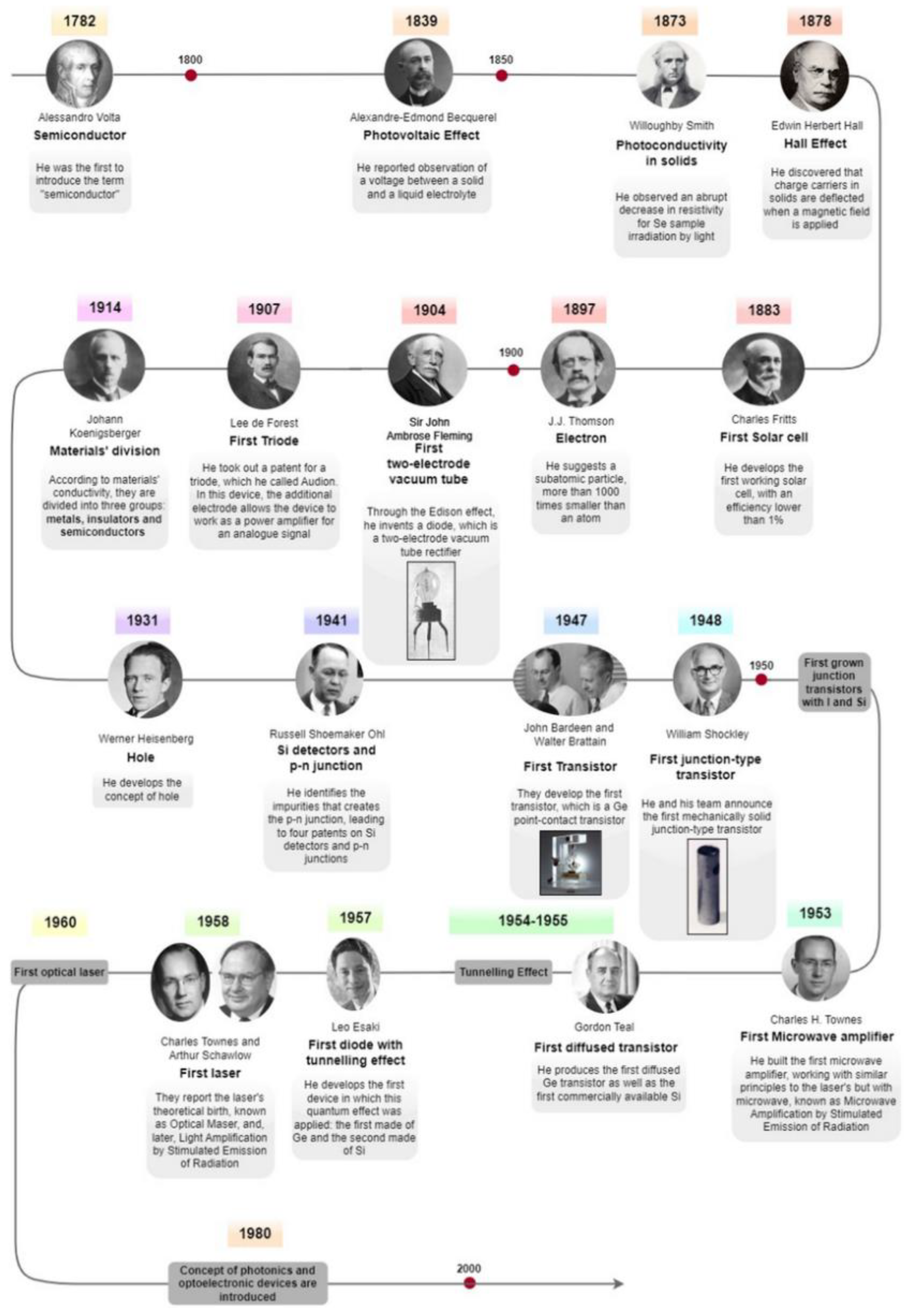
2.3. Historical Development of Wide-Bandgap (WBG) Semiconductors

The history of semiconductors is encapsulated by major discoveries, starting with Alessandro Volta, who, in 1782, coined the term "semiconductor," providing a name that would form the groundwork for other explorations to come (Figure 4) [50]. The photovoltaic effect, discovered by Alexandre-Edmond Becquerel in 1839, was pivotal for modern solar technology, culminating in Charles Fritts' creation of the first solar cell in 1883 using selenium (Figure 4) [51]. In the early 20th century, Sir John Ambrose Fleming was credited for pioneering the invention of the vacuum tube in 1904 (Figure 4). This was then followed by the discovery of the first commercial silicon transistor by John Bardeen and Walter Brattain in 1947 (Figure 4), establishing silicon as the dominant semiconductor material [39] However, by the 1990s, silicon's limitations in high-power and high-temperature applications prompted research into alternative materials like silicon carbide (SiC) and gallium nitride (GaN), recognized as Wide-Bandgap semiconductors [38,52]. This evolution reflects the ongoing quest for improved semiconductor performance and applications.

Emergence of SiC and GaN

Silicon Carbide (SiC) power devices, developed in the 1990s, have significantly transformed the semiconductor industry by enabling high-temperature applications due to their exceptional properties, such as high thermal conductivity and electric field strength, making them ideal for power electronics in electric vehicles and renewable energy systems [53,54]. Concurrently, Gallium Nitride showed up in the early 2000s as a key material for high-frequency electronics: better breakdown voltage and switching speed compared to traditional silicon semiconductors, making it crucial for high-performance applications [41]. The advancements in Wide-Bandgap (WBG) materials like SiC and GaN not only enhance efficiency but also allow operation at higher voltages and temperatures, facilitating innovations in power management systems and contributing to sustainability efforts within the technology sector [55]. This evolution in semiconductor technology marks a pivotal shift, driving the development of more efficient and reliable power electronics.

Pivotal Technological Advancements

The Power Electronic Building Block (PEBB) program, initiated in 1994, significantly advanced Silicon Carbide (SiC) technology by focusing on reducing size, weight, and cost for military power electronics, which also benefited commercial sectors like electric vehicles [56]. SiC devices have shown remarkable capabilities, handling voltages up to 20 kV, making them ideal for applications in electric vehicle powertrains and energy storage systems [41]. Concurrently, Gallium Nitride (GaN) devices gained traction for their efficiency in power conversion, particularly in electric vehicles where compact and energy-efficient designs are essential [41]. By the mid-2000s, Wide-Bandgap (WBG) semiconductors, including SiC and GaN, demonstrated significant performance enhancements, with GaN devices achieving switching frequencies up to 2 MHz, which is beneficial for fast chargers and RF amplifiers [41,57]. This synergy between military and commercial applications has propelled the development of advanced power electronics technologies.

Impact on Modern Applications

The integration of Wide-Bandgap (WBG) semiconductors—most prominently Gallium Nitride and Silicon Carbide—has considerably modernized applications in contemporary electric vehicle and renewable energy sectors. These materials exhibit superior properties such as high electron mobility, high breakdown voltage, and excellent thermal conductivity, which enable more efficient and compact power management systems, thereby enhancing the vehicle’s performance and range in EVs [7,41]. In renewable energy systems, SiC devices have notably improved the efficiency of photovoltaic inverters, minimizing energy losses and costs associated with solar energy conversion [2]. Furthermore, both GaN and SiC are pivotal in revolutionizing power supply systems by reducing energy losses during conversion processes, contributing to sustainability efforts aimed at lowering carbon footprints [58,59]. Emerging WBG materials like aluminum phosphide, diamond, and boron nitride also show promise due to their superior properties, such as high thermal conductivity and breakdown strength, which are essential for high-power applications in extreme environments [13]. Collectively, all these developments together contribute to the global efforts aimed at tackling modern energy-related problems and minimizing the carbon footprint [7,41].

Evolution Toward Sustainable Manufacturing

The transition to sustainable manufacturing is very crucial, especially in WBG semiconductor manufacturing, since the sector involves highly energy-intensive processes with environmentally toxic by-products. Conventionally, the manufacturing industry has faced severe impacts on the environment, arousing the need for development toward sustainability that would also corroborate green manufacturing principles. Strategies such as renewable energy integration, energy efficiency measures, and waste reduction are critical in mitigating ecological impacts and reducing carbon footprints [22,60]. Various technological innovations like the integration of Interne of all Things (IoT), Artificial Intelligence (AI), Machine Learning (ML), Robotics and automation have driven recent transitions to sustainable manufacturing, including smart manufacturing systems for optimization in resource use with minimal wastage [61], [62,63,64]. Despite the growing interest in Sustainable Product Development (SPD), the adoption of these practices remains limited, indicating a substantial opportunity for improvement in the industry [31]. Given the continuous demand for electronic devices, there is a further need to enhance the sustainability of the semiconductor manufacturing industry due to increased scrutiny and interest in environmental stewardship

Environmental Impact of Manufacturing

The manufacturing of Wide-Bandgap (WBG) semiconductors, particularly Silicon Carbide (SiC) and Gallium Nitride (GaN), is indeed resource-intensive and poses significant environmental challenges. The reliance on fossil fuels during production contributes to substantial carbon emissions, while the processes generate hazardous chemical byproducts that threaten air and water quality [49]. During the wafer fabrication process, significant emissions of non-methane hydrocarbons (NMHCs) occur, particularly from processes such as photolithography, which has the highest untreated emissions rates [65]. These NMHCs, including solvents like acetone and methanol, can contribute to air pollution and human toxicity [65]. As the demand for WBG devices grows, especially in sectors like electric vehicles and renewable energy systems, there is an urgent need to adopt cleaner and more efficient manufacturing methods to mitigate these impacts [9]. Furthermore, the lifecycle of WBG technology, from raw material supply to end-of-life disposal, necessitates a comprehensive approach to sustainability, emphasizing the importance of proper disposal of toxic substances [49]. Research into the environmental aspects of WBG materials is still emerging, highlighting the need for policymakers to develop informed strategies that promote sustainable practices within the semiconductor industry [49].

Current Innovations

Recent innovations in Wide-Bandgap (WBG) semiconductor manufacturing are significantly addressing environmental impacts through enhanced energy efficiency and waste reduction strategies. Advances in epitaxial growth techniques are optimizing energy use, thereby lowering greenhouse gas emissions associated with production processes, which is a crucial step in mitigating the environmental challenges of traditional manufacturing methods [24]. The semiconductor industry is increasingly adopting closed-loop recycling systems, allowing for the recovery and reuse of materials like silicon wafers. This practice not only conserves raw materials but also minimizes waste, preventing substantial amounts of semiconductor waste from entering landfills [14]. The integration of green chemistry principles is reducing the reliance on hazardous substances, leading to a decrease in toxic waste generation during production [22]. The green chemistry principles emphasize on the design of chemical products and processes that minimize or eliminate the use and generation of hazardous substances. For instance, the use of aliphatic amino acids as environmentally friendly corrosion inhibitors in Chemical Mechanical Planarization (CMP) slurries exemplifies this approach, replacing more toxic alternatives like benzotriazole (BTA) [24]. All these innovations together indeed represent a great leap forward toward greener semiconductor manufacturing—ensuring a healthier environment for production and rising to the call for global sustainability.

Integration of Industry 4.0 and Reconfigurable Technologies

The integration of Industry 4.0 technologies, such as Cyber-Physical Systems (CPS), the Internet of Things (IoT), and Artificial Intelligence (AI), is revolutionizing manufacturing processes by enhancing resource management and minimizing emissions, particularly in semiconductor production [66,67]. These intelligent manufacturing systems facilitate real-time data analysis and automation, allowing for adaptive manufacturing that can swiftly respond to changing market demands [68,69]. Reconfigurable technologies play a crucial role in this transformation, enabling manufacturers to fine-tune their processes dynamically, which not only boosts production efficiency but also significantly reduces waste and environmental impact [66,70]. By leveraging these advanced technologies, industries can achieve higher operational effectiveness and sustainability, positioning themselves competitively in the evolving digital landscape [67,68]

Toward a Circular Economy

The semiconductor industry is increasingly embracing circular economy principles to enhance sustainability by optimizing resource utilization and minimizing waste throughout the product lifecycle. This shift involves the integration of digital technologies such as IoT, AI, and blockchain, which improve visibility and traceability in supply chains, thereby facilitating the reuse and recycling of materials from raw material extraction to end-of-life disposal [64,71]. A structured framework for sustainable manufacturing is thus relevant to help organize the efforts of industry in the direction of resource conservation and address the complexities surrounding green supply chain management. [29]. The adoption of circular economy practices not only mitigates environmental impacts but also promotes economic benefits through innovative business models that prioritize waste reduction and resource efficiency [72,73]. As policymakers and industry leaders recognize these advantages, the momentum toward a more resilient and eco-friendlier semiconductor industry continues to grow [71].

3. WBG Semiconductor Manufacturing

3.1. GaN and SiC Semiconductor Manufacturing Route

GaN Manufacturing Route

The manufacturing of gallium nitride (GaN) involves several critical steps to ensure that the layers are high-quality and suitable for advanced electronic applications. It begins with substrate preparation, where materials like sapphire, silicon, and silicon-on-insulator (SOI) are cleaned and patterned to create a defect-free surface for GaN growth [74]. Epitaxial growth is primarily achieved through Metal-Organic Chemical Vapor Deposition (MOCVD), where GaN is deposited from metal-organic precursors at elevated temperatures, often utilizing a buffer layer to enhance the quality of the film [59,75]. The growth process can be tailored to form structures such as AlGaN/GaN heterostructures, which are essential for high electron mobility transistors (HEMTs) [75]. Doping is performed via ion implantation techniques (e.g., magnesium for p-type conductivity), optimized to minimize damage and enhance ion activation [76]. Additionally, etching processes, including photoelectrochemical etching, are employed to create deep trench structures that improve heat dissipation and reduce parasitic capacitance. Finally, photolithography is used for pattern definition, followed by metal contact deposition, culminating in the dicing and packaging of the final devices for integration into electronic systems [59].

SiC Manufacturing Route

Silicon Carbide (SiC) substrates are primarily produced using the physical vapor transport (PVT) technique, which is essential for achieving high-quality single crystals due to the limitations of traditional melt-based methods [77,78]. Following substrate production, the wafers undergo polishing to ensure a smooth surface, which is critical for subsequent epitaxial growth using chemical vapor deposition (CVD) techniques that allow precise control over layer thickness and composition [77,79]. Doping is achieved through ion implantation or diffusion, with nitrogen for n-type and aluminum for p-type doping, necessitating careful control to maintain material integrity [80]. Reactive ion etching (RIE) is employed for patterning SiC wafers, ensuring minimal damage to the substrate [81]. Finally, photolithography is used for device fabrication, where metal contacts are deposited and annealed to ensure good electrical connectivity, followed by rigorous testing before packaging for applications in power converters and electric vehicles [77].

3.2. Innovations in WBG Semiconductor Manufacturing

The growing demand for Wide-bandgap (WBG) semiconductors, such as silicon carbide (SiC) and gallium nitride (GaN), along with Ultrawide-Bandgap materials like gallium oxide (Ga2O3) necessitates a focus on sustainable manufacturing practices to mitigate energy consumption, manage toxic byproducts, and address resource depletion [43]. The challenges associated with doping these semiconductors, which can lead to inefficiencies and increased waste, further emphasize the need for innovative approaches in their production [82]. As the industry evolves, integrating sustainability into the development and manufacturing processes of WBG materials will be crucial for meeting both performance and environmental goals [5,42].
The concept of the circular economy has been increasingly applied in the field of semiconductors as a principle for better sustainability by recycling and reusing. Wafer reclaiming exemplifies this approach, where used silicon wafers are polished and reused, significantly reducing the demand for new silicon extraction and minimizing semiconductor waste disposal (Table 2) [23]. Recovery techniques for valuable materials like gallium and silicon from production byproducts are being integrated into manufacturing processes, allowing for the reuse of materials previously deemed waste [83]. This aligns with broader circular economy models that emphasize resource preservation and waste reduction, as seen in various industries, including minerals and metals, where similar recovery and recycling strategies are implemented [84]. Closed-loop manufacturing systems are also being explored to reintegrate production waste into the manufacturing cycle, thereby further decreasing the environmental footprint of semiconductor production (Table 2) [85]. Collectively, these practices contribute to achieving sustainable development goals and enhancing the overall efficiency of the semiconductor industry.
The transition toward sustainable Wide-Bandgap (WBG) semiconductor manufacturing is increasingly focused on reducing energy consumption during production, particularly in energy-intensive processes like Chemical Vapor Deposition (CVD) (Figure 5a). Innovations such as low-temperature/pressure CVD (Figure 5b, Table 2) and Atomic Layer Deposition (ALD) (Figure 5c) are emerging as energy-efficient alternatives, allowing for the production of high-quality films at significantly lower temperatures, thus minimizing energy usage [24]. Additionally, Molecular Beam Epitaxy (MBE) (Figure 5d) employs controlled, low-energy processes that enhance material quality while further reducing energy requirements [24]. The semiconductor foundry industry, which has historically faced challenges related to high energy and water consumption, is also exploring these advanced techniques to mitigate its environmental impact [14]. By integrating renewable energy sources (Table 2) and optimizing manufacturing processes, the industry can achieve substantial reductions in greenhouse gas emissions and waste generation, aligning with broader sustainability goals [22,86].
The semiconductor industry faces significant environmental and health challenges due to the use of toxic chemicals like hydrogen fluoride (HF) in manufacturing processes. To address these concerns, there is a growing emphasis on green chemistry approaches aimed at reducing or eliminating hazardous substances (Table 2). Research is in progress to establish alternative chemical agents that could replace HF in such applications with minimum risk to health and the environment [24]. Innovative methods for capturing and recycling harmful byproducts are being implemented, allowing manufacturers to convert waste chemicals into reusable materials, thus preventing emissions and reducing reliance on toxic substances [91,92]. The adoption of less hazardous chemicals and stringent chemical management protocols is crucial for safeguarding worker health and ensuring compliance with environmental regulations [93]. These are methodologies and strategies that, in combination, contribute to a much more sustainable semiconductor manufacturing process and hence support the innovation required by the industry while addressing environmental sustainability. [14].
Advanced Industry 4.0 technologies, more so AI, machine learning, and digital twin integration, have manifold increased sustainability in WBG semiconductor manufacturing. AI-based manufacturing systems analyze large volumes of data to identify inefficiencies and optimize resource utilization, thereby reducing waste and energy consumption (Figure 6) [94,95]. Machine learning algorithms forecast equipment maintenance to avoid breakdowns and defective products, which further reduces material waste [96]. Digital twin technology creates virtual replicas of production processes, allowing manufacturers to simulate various scenarios and identify energy-efficient approaches, thus expediting the adoption of energy-saving techniques [96,97]. Reconfigurable manufacturing systems enable dynamic adaptation of production lines to meet changing demands, optimizing resource use and minimizing waste [98]. These technological advancements will help create a more sustainable manufacturing environment by helping improve efficiency and reducing environmental impact.
The semiconductor industry faces significant challenges in achieving sustainability, particularly concerning the sourcing of critical materials like gallium and silicon, often extracted from regions with inadequate environmental and labor regulations. This raises ethical concerns related to environmental degradation and human rights abuses [100]. To combat these issues, companies must implement robust traceability systems that ensure responsible sourcing of raw materials, as some manufacturers have begun to adopt tracking systems to enhance transparency and confirm ethical sourcing [101]. However, widespread adoption across the industry is essential to align the entire supply chain with sustainability goals [102]. The historical trends indicate a pressing need for improved environmental performance, highlighted by the increase in hazardous waste generation despite technological advancements [29]. Collaborative efforts and regulatory mechanisms are crucial in facilitating ethical procurement practices, thereby enhancing sustainability within the semiconductor supply chain [100,102].
The semiconductor industry, particularly in the production of Wide-Bandgap (WBG) materials like silicon carbide (SiC) and gallium nitride (GaN), faces significant challenges due to the depletion of critical resources such as silicon and gallium. To address these challenges, ongoing research is focused on enhancing material efficiency through innovations in nanotechnology, which allows for the development of devices that utilize fewer materials without compromising performance, thereby reducing environmental impact and aligning with sustainability goals [29]. Additionally, the adoption of green supply chain management practices is crucial for improving resilience and mitigating risks associated with resource scarcity [29]. The semiconductor foundry industry is also increasingly investing in renewable energy sources, such as solar power, to lower greenhouse gas emissions during manufacturing processes [14]. These combined efforts are essential for ensuring the long-term viability of WBG semiconductor production in the face of resource constraints and environmental concerns [103,104].
Government policies and regulatory frameworks are indeed pivotal in steering the semiconductor industry towards sustainable manufacturing practices. The European Union's Green Deal exemplifies this by setting ambitious emission reduction targets and promoting sustainable processes across industries, including semiconductors [105]. In the U.S., both federal and state initiatives incentivize investments in energy-efficient technologies, compelling companies to adopt greener practices [29]. This regulatory pressure not only ensures compliance with environmental standards but also fosters innovation, as companies seek to enhance sustainability while remaining competitive in a global market [14,92]. Furthermore, the semiconductor industry's inherent complexities necessitate a robust approach to green supply chain management, which can be facilitated by appropriate policies and regulations [29]. As the industry evolves, sustainability emerges as a critical driver of innovation, reinforcing the notion that environmental responsibility is integral to long-term competitiveness [24].

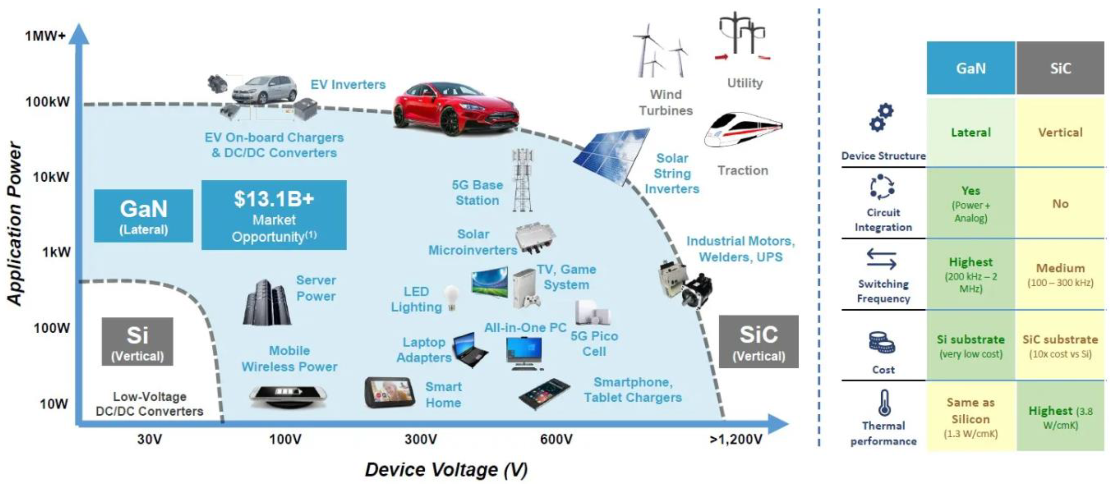
4. Applications of Wide-Bandgap (WBG) Semiconductors in Sustainable Technologies

Wide-bandgap (WBG) semiconductors, specifically Silicon Carbide (SiC) and Gallium Nitride (GaN), have gained significant attention for their transformative impact on various industries, especially in the pursuit of sustainable technologies. These materials are driving innovation in electric vehicles (EVs), renewable energy systems, 5G infrastructure, smart grids, and other crucial applications (Figure 7). The integration of SiC and GaN in these technologies contributes to improved energy efficiency, reduced carbon emissions, and overall sustainability.
Silicon Carbide (SiC) devices are transforming electric vehicle (EV) power systems (Figure 7) by significantly enhancing the efficiency of inverters and power modules. These components outperform traditional silicon systems, achieving efficiencies exceeding 95% and thereby minimizing energy losses during power conversion, which is crucial for optimizing energy use in EV traction inverters [53,107]. SiC technology allows for operation at higher voltages and temperatures, further reducing energy losses and improving powertrain efficiency, which translates into extended driving ranges and reduced recharging frequency [108]. Additionally, SiC's capability to handle higher switching frequencies facilitates faster energy transfer, leading to quicker charging times for EVs [109]. This efficiency not only enhances vehicle performance but also supports the transition to cleaner transportation by lowering energy consumption and reducing the carbon footprint of EVs, promoting sustainability in the automotive sector [108,110].
Gallium Nitride (GaN) transistors are revolutionizing renewable energy systems, particularly in solar inverters and wind turbine power electronics (Figure 7), due to their ability to handle high voltages and frequencies with minimal energy loss. This capability is crucial for managing the fluctuating nature of renewable energy sources, enhancing the robustness of designs in these applications [58,111]. GaN technology significantly improves power conversion efficiency, which facilitates better integration of renewable energy into power grids, leading to higher energy yields from solar panels and wind turbines [112,113]. By minimizing energy losses during power conversion, GaN devices not only support sustainability goals by maximizing output from renewable resources but also reduce overall energy waste [114]. As these systems become more efficient and reliable, the adoption of solar and wind energy is expected to increase, further decreasing reliance on fossil fuels and contributing to a cleaner, more sustainable energy future [113,114].
The integration of Gallium Nitride (GaN) semiconductors into 5G infrastructure (Figure 7) significantly enhances sustainability by enabling higher frequency operations with reduced power consumption compared to traditional silicon devices. This efficiency leads to lower energy usage in 5G base stations, which is crucial for meeting the growing data demands of modern communication networks while adhering to sustainable practices [58]. GaN's ability to minimize heat generation reduces cooling requirements, resulting in substantial energy savings [7]. The compact design of GaN-based equipment further decreases the energy and resources needed for infrastructure development, facilitating faster data transmission with lower energy consumption [115]. GaN and Silicon Carbide (SiC) devices improve smart grid efficiency by reducing energy losses during transmission and distribution, optimizing grid performance, and supporting the integration of renewable energy sources [116]. This combination of advancements promotes sustainability through the effective utilization of clean energy resources and enhances overall grid stability [117].
Sectors other than electric vehicles and renewable energy systems (Figure 7) have been the nascent target of Wide-Bandgap semiconductors. In aerospace and military applications, these materials are essential for high-temperature and high-power systems, enhancing reliability and energy efficiency in mission-critical operations under extreme conditions [41,58]. Their superior properties, such as high breakdown voltage and good thermal conductivity, greatly improve their performance while cutting down on energy consumption [41]. In consumer electronics, WBG semiconductors are increasingly used in chargers and power supplies, leading to lower energy consumption in everyday devices [2]. This transition not only aligns with sustainability goals by promoting efficient technologies but also helps minimize electronic waste [118]. As WBG technologies continue to evolve, they are poised to drive innovation and support the global shift towards greener technologies across multiple industries [2,7].

5. Challenges and Future Prospects of Wide-Bandgap (WBG) Semiconductors

To fully realize the potential and enable the widespread adoption of WBG semiconductors, several significant challenges must be addressed. These challenges span across cost and scalability, material availability, integration with existing technologies, and environmental sustainability, each of which will be explored in detail.

Cost and Scalability

The high cost and complexity of producing Wide-Bandgap (WBG) semiconductors, such as SiC and GaN, significantly hinder their large-scale adoption. Despite advancements in fabrication techniques, these processes remain intricate and expensive, leading to lower production yields compared to traditional silicon semiconductors, which complicates achieving necessary economies of scale [119]. The capital-intensive nature of WBG semiconductor production, particularly the requirement for specialized equipment and cleanroom environments, poses additional challenges for scaling up manufacturing [119]. The production of vertical-cavity surface-emitting lasers (VCSELs) from materials like Gallium Arsenide (GaAs) and Aluminum Gallium Arsenide (AlGaAs) faces issues related to thickness and wavelength uniformity, which exemplify the broader difficulties in manufacturing next-generation semiconductors [119]. These limitations collectively inhibit mass production, which is essential for the widespread implementation of WBG technologies [119,120].
Future Prospects; The future of manufacturing techniques for Wide-Bandgap (WBG) semiconductors, particularly Gallium Nitride (GaN), is focused on enhancing scalability and reducing production costs through automation and advanced wafer technologies. Research indicates that improvements in manufacturing processes, such as Metal-Organic Vapor Phase Epitaxy (MOVPE), are essential for achieving uniformity and yield in larger diameter wafers, which is critical for applications in photonics and beyond [119]. The semiconductor industry is increasingly prioritizing energy-efficient chips and sustainable practices, driven by environmental concerns and market demands [121]. The life cycle impacts of WBG materials, including their energy consumption and greenhouse gas emissions, are also being evaluated to support a circular economy [49]. As these innovations unfold, they will be pivotal in realizing the potential of WBG semiconductors in sustainable applications like electric vehicles and renewable energy systems, ultimately contributing to an eco-friendlier technological landscape [59,122].

Material Availability and Sustainability

The transition to Wide-Bandgap (WBG) semiconductors faces significant challenges related to material availability and sustainability. The limited supply of these critical materials, exacerbated by global competition, creates vulnerabilities in the supply chain that can delay production and hinder the adoption of WBG technologies [123]. The extraction and refinement processes for SiC and GaN are energy-intensive, contributing to their environmental footprint, which is a growing concern in the context of sustainable development [124,125]. The demand of these materials by the automotive and construction industries is increasingly high because of their ever-growing need for lightweight yet highly efficient materials. This may lead to further price volatility, thus complicating the sustainable transition towards electric vehicles and other advanced technologies [126,127]. Addressing these challenges requires coordinated efforts in research and development, as well as the exploration of alternative materials that minimize environmental impacts [124].
Future Prospects: Research into alternative materials and advanced recycling processes is crucial for addressing the risks of raw material shortages, particularly in the context of the semiconductor industry. The European Union has recognized the importance of critical raw materials (CRMs) and is actively promoting innovative recycling technologies to enhance material recovery from electronic waste, such as Printed Circuit Boards (PCBs) and Rare Earth Permanent Magnets (RE-PMs) [128]. The construction industry’s shift towards using waste materials exemplifies the broader movement towards a circular economy, which emphasizes resource conservation and waste reduction [129]. Integrating sustainable materials into supply chains can significantly reduce carbon footprints and enhance resilience, although challenges such as higher costs and regulatory complexities remain [130]. The need for comprehensive policies and harmonization across EU member states is essential to facilitate the transition towards sustainable practices and ensure a stable supply of essential materials for industries like semiconductors [131,132].

Integration with Existing Technologies

The transition from traditional silicon-based semiconductors to Wide-Bandgap (WBG) semiconductors poses significant integration challenges for existing technologies. Industries like automotive and telecommunications must invest heavily in upgrading their infrastructures to accommodate these new materials, which can delay widespread adoption due to the substantial modifications required for power electronics and thermal management systems [2,49]. The integration process is complicated by issues such as lattice mismatches, which can lead to defects that adversely affect the performance and reliability of WBG devices [133]. To address these challenges, advanced device architectures must be developed to optimize performance while ensuring manufacturability, thereby facilitating a smoother transition to WBG technologies [134,135]. Ultimately, overcoming these integration hurdles is crucial for unlocking the full potential of WBG semiconductors in modern applications.
Future Prospects: The transition from silicon to Wide-Bandgap (WBG) semiconductors is being facilitated through hybrid technologies that allow for the coexistence of both materials, enabling industries to adapt gradually without extensive system overhauls. For instance, the Si/WBG hybrid half-bridge converters optimize power-sharing and switching frequency, achieving significant reductions in power loss while maintaining performance quality, thus demonstrating a practical approach to integrating WBG devices with existing silicon technology [136]. The use of WBG materials like SiC and GaN in power converters enhances efficiency and performance in electric vehicles, addressing the growing demand for high power density and efficiency [2,11]. Ongoing research into defect control and device optimization, particularly in Ultrawide-Bandgap materials, is crucial for improving their reliability and performance, which will further accelerate their adoption across various sectors [13]. This gradual integration model is essential for meeting industry demands while minimizing disruption [137].

Ultrawide-Bandgap (UWBG) Materials

Ultrawide-Bandgap (UWBG) materials, including Diamond, Gallium Oxide (Ga₂O₃), and Aluminum Nitride (AlN), are poised to revolutionize high-power applications due to their superior performance characteristics compared to traditional Wide-Bandgap (WBG) semiconductors. These materials can enhance energy efficiency, minimize energy losses, and facilitate the miniaturization of high-power devices, which is essential for sectors like aerospace and high-voltage power grids [5,13]. Significant challenges persist in their fabrication, such as high production costs, defects during synthesis, and the difficulty of producing large, defect-free wafers [82,138]. These manufacturing limitations are reminiscent of those encountered with WBG semiconductors, underscoring the urgent need for innovative production techniques to enable the widespread adoption of UWBG materials in advanced electronic applications [13,42].
Future Prospects: Ongoing research into Ultrawide-Bandgap (UWBG) materials is crucial for overcoming existing barriers related to their fabrication and performance. The challenges include achieving bipolar electrical conductivity and effective doping, particularly for p-type regions, which are essential for high-voltage applications [138,139]. Investments from both public and private sectors are vital to develop cost-effective and scalable production technologies, which can enhance the understanding and application of UWBG materials like AlGaN, Ga2O3, and Diamond [5,13]. Improved fabrication methods, such as magnetron sputtering for p-type doping, are being explored to create high-performance devices that can operate efficiently under extreme conditions [139]. Addressing these challenges could lead to significant advancements in high-power applications, paving the way for the next generation of energy-efficient technologies that leverage the superior properties of UWBG semiconductors [5,13].

Long-Term Sustainability and Environmental Impact

Wide-Bandgap (WBG) semiconductors, such as silicon carbide (SiC) and gallium nitride (GaN), offer significant advantages in reducing energy consumption and carbon emissions in power electronics applications due to their superior performance characteristics [7,140]. However, the production processes for these materials are energy-intensive and raise sustainability concerns. The semiconductor foundry industry has seen a substantial increase in hazardous waste generation, with a 239% rise in absolute values over the past decade, despite advancements in renewable energy usage that have reduced greenhouse gas emissions per manufacturing index by 32% [14]. The challenges associated with material extraction and processing of WBG semiconductors necessitate a shift towards more environmentally conscious practices to mitigate their ecological footprint [5]. Addressing these issues is crucial for ensuring that the benefits of WBG technologies do not come at the expense of long-term environmental sustainability [141].
Future Prospects: To align with global sustainability goals, the semiconductor industry must prioritize energy-efficient fabrication techniques and the use of renewable energy sources in production facilities. Recent studies highlight that the industry's energy-intensive processes contribute significantly to environmental degradation, with a notable increase in hazardous waste generation over the past decade [14]. The development of greener chemical processes, such as the use of environmentally friendly corrosion inhibitors in Chemical Mechanical Planarization (CMP) slurries, is crucial for reducing the environmental footprint of semiconductor manufacturing. Adopting a green supply chain management approach can enhance sustainability by addressing technological risks and improving resource utilization [29,142]. As the semiconductor industry evolves, it is essential to invest in research and development to create energy-efficient technologies and minimize electronic waste, ensuring that advancements in Wide-Bandgap (WBG) semiconductors contribute to a cleaner and greener future [121,142].

6. Conclusions

Wide-bandgap (WBG) semiconductors, particularly silicon carbide (SiC) and gallium nitride (GaN), represent a key advancement in the quest for higher energy efficiency and performance in high-power applications. However, their production methods remain energy-intensive, with significant environmental challenges such as high carbon emissions and waste generation. To mitigate these impacts, the integration of green manufacturing practices, including energy-efficient epitaxial growth, the adoption of circular economy principles, and the development of low-toxicity chemicals for wafer processing, is critical. Additionally, innovative recycling techniques for recovering materials from end-of-life WBG devices can substantially reduce electronic waste.
Future research should prioritize improving the sustainability of ultrawide-bandgap (UWBG) materials like gallium oxide (Ga₂O₃) and diamond, which offer even greater performance but face similar environmental hurdles. These innovations, combined with more stringent regulatory frameworks and industry collaboration, can pave the way for WBG semiconductors to contribute meaningfully to global sustainability goals in sectors such as renewable energy, electric vehicles, and telecommunications. Addressing these challenges head-on will be essential for balancing the growth of WBG technologies with the environmental responsibilities of the semiconductor industry.

Author Contributions

The manuscript was written through contributions of all authors. All authors have approved the final version of the manuscript.

Data Availability Statement

No data was used for the research described in the article

Conflicts of Interest

The authors declare that they have no known competing financial interests or personal relationships that could have appeared to influence the work reported in this paper.

References

  1. S. Yuvaraja, V. Khandelwal, X. Tang, and X. Li, “Wide bandgap semiconductor-based integrated circuits,” Chip, vol. 2, no. 4, p. 100072, Dec. 2023. [CrossRef]
  2. H. Prasad Bhupathi et al., “Investigation of WBG based Power Converters used in E-Transportation,” E3S Web of Conferences, vol. 552, p. 01145, Jul. 2024. [CrossRef]
  3. B. Chandran et al., “Solar-Driven Sustainability: III–V Semiconductor for Green Energy Production Technologies,” Nano-Micro Letters 2024 16:1, vol. 16, no. 1, pp. 1–34, Jul. 2024. [CrossRef]
  4. K. Shenai, M. Bakowski, and N. Ohtani, “Foreword special issue on wide bandgap power switching devices for energy efficiency and renewable energy integration,” IEEE Trans Electron Devices, vol. 62, no. 2, pp. 245–247, Feb. 2015. [CrossRef]
  5. K. Woo et al., “From wide to ultrawide-bandgap semiconductors for high power and high frequency electronic devices,” Journal of Physics: Materials, vol. 7, no. 2, p. 022003, Mar. 2024. [CrossRef]
  6. O. S. Chaudhary, M. Denaï, S. S. Refaat, and G. Pissanidis, “Technology and Applications of Wide Bandgap Semiconductor Materials: Current State and Future Trends,” Energies 2023, Vol. 16, Page 6689, vol. 16, no. 18, p. 6689, Sep. 2023. [CrossRef]
  7. G. Forte and A. Spampinato, “High Power-Density Design Based on WBG GaN Devices for Three-Phase Motor Drives,” 2024 International Symposium on Power Electronics, Electrical Drives, Automation and Motion, SPEEDAM 2024, pp. 65–70, 2024. [CrossRef]
  8. A. ; H. Obdan, Y. Ye, T. Pajchrowski, A. Erken, and A. H. Obdan, “Examining the Optimal Use of WBG Devices in Induction Cookers,” Applied Sciences 2023, Vol. 13, Page 12517, vol. 13, no. 22, p. 12517, Nov. 2023. [CrossRef]
  9. Q. Wang et al., “(Invited) Wide Bandgap Semiconductor Based Devices for Digital and Industrial Applications,” ECS Trans, vol. 112, no. 2, p. 37, Sep. 2023. [CrossRef]
  10. T. McDonald, “Power Conversion Semiconductor and Circuit Trends and Challenges for a Sustainable Energy Future,” Technical Digest - International Electron Devices Meeting, IEDM, 2023. [CrossRef]
  11. K. P. Krovi, P. Skarolek, and J. Bauer, “Comparison of Bi-Directional DC/DC Converter using Si and WBG Devices,” 2023 International Conference on Electrical Drives and Power Electronics, EDPE 2023 - Proceedings, 2023. [CrossRef]
  12. B. Vanhouche et al., “Environmental Analysis of RF Substrates,” 2024 Electronics Goes Green 2024+ (EGG), pp. 1–8, Jun. 2024. [CrossRef]
  13. E. L. Piner and M. W. Holtz, “(Invited) Heterogeneous Integration of Ultrawide Bandgap III-Nitrides and Diamond,” ECS Meeting Abstracts, vol. MA2023-02, no. 32, p. 1580, Dec. 2023. [CrossRef]
  14. M. Ruberti, “Environmental performance and trends of the world’s semiconductor foundry industry,” J Ind Ecol, 2024. [CrossRef]
  15. C. J. M. Lawley et al., “Geospatial Data and Deep Learning Expose ESG Risks to Critical Raw Materials Supply: The Case of Lithium,” Earth Science, Systems and Society, vol. 4, p. 10109, Jul. 2024. [CrossRef]
  16. O. Akyıldız, “The Importance of Silicon Metal on the Green Transition and the Role of Northern Countries in the Silicon Metal Market,” EGU24, Mar. 2024. [CrossRef]
  17. Y. Mei, Y. Geng, Z. Chen, S. Xiao, and Z. Gao, “Ensuring the sustainable supply of semiconductor material: A case of germanium in China,” Int J Prod Econ, vol. 271, p. 109231, May 2024. [CrossRef]
  18. “Semiconductor Market Size to Surpass USD 1,137.57 Billion by 2033.” Accessed: Sep. 24, 2024. [Online]. Available: https://www.precedenceresearch.com/semiconductor-market.
  19. A. Machín, M. C. Cotto, F. Díaz, J. Duconge, C. Morant, and F. Márquez, “Environmental Aspects and Recycling of Solid-State Batteries: A Comprehensive Review,” Batteries 2024, Vol. 10, Page 255, vol. 10, no. 7, p. 255, Jul. 2024. [CrossRef]
  20. K. Dhivya and G. Premalatha, “E-Waste Challenges & Solutions,” Sustainable Management of Electronic Waste, pp. 255–275, Jan. 2024. [CrossRef]
  21. M. C. Jena, S. K. Mishra, and H. S. Moharana, “Challenges and way forward in the handling and disposal of battery waste: Towards sustainable practices,” Sustainable Social Development, vol. 2, no. 4, p. 2866, Aug. 2024. [CrossRef]
  22. P. Suresh et al., “Strategies for Carbon Footprint Reduction in Advancing Sustainability in Manufacturing,” https://services.igi-global.com/resolvedoi/resolve.aspx?doi=10.4018/979-8-3693-3625-0.ch012, Jan. 1AD. [CrossRef]
  23. A. Fontana et al., “Enhancing the Sustainability of the Electronics in the Automotive Sector in the Context of Circular Economy Through a Decision-Making Framework,” IEEE Xplore, Jun. 2024, Accessed: Sep. 16, 2024. [Online]. Available: https://ieeexplore.ieee.org/document/10631249.
  24. Ji. Seo, “Bridging Technology and Environment: Sustainable Approaches in Semiconductor Chemical Mechanical Planarization (CMP),” ECS Meeting Abstracts, vol. MA2024-01, no. 20, p. 1272, Aug. 2024. [CrossRef]
  25. A. E. Esiri, O. A. Babayeju, I. O. Ekemezie, A. E. Esiri, O. A. Babayeju, and I. O. Ekemezie, “Implementing sustainable practices in oil and gas operations to minimize environmental footprint,” https://gsconlinepress.com/journals/gscarr/sites/default/files/GSCARR-2024-0207.pdf, vol. 19, no. 3, pp. 112–121, Jun. 2024. [CrossRef]
  26. S. Reynolds, “Sustainable Supply Chain Practices- A Qualitative Investigation of Green Logistics Strategies,” Jun. 2024. [CrossRef]
  27. K. Makprang, “SUSTAINABILITY IN SUPPLY CHAINS: STRATEGIES AND PRACTICES FOR A GREENER FUTURE,” RMUTT GLOBAL BUSINESS ACCOUNTING AND FINANCE REVIEW, vol. 8, no. 1, pp. 85–108, Jun. 2024. [CrossRef]
  28. J. Chen and L. Gan, “Lenovo’s Green Supply Chain Management Framework for Green Development of Enterprises,” Frontiers in Business, Economics and Management, vol. 15, no. 3, pp. 61–69, Jul. 2024. [CrossRef]
  29. R. Chaudhuri, B. Singh, A. K. Agrawal, S. Chatterjee, S. Gupta, and S. K. Mangla, “A TOE-DCV approach to green supply chain adoption for sustainable operations in the semiconductor industry,” Int J Prod Econ, vol. 275, p. 109327, Sep. 2024. [CrossRef]
  30. T. Feng, M. Qamruzzaman, S. S. Sharmin, and S. Karim, “Bridging Environmental Sustainability and Organizational Performance: The Role of Green Supply Chain Management in the Manufacturing Industry,” Sustainability 2024, Vol. 16, Page 5918, vol. 16, no. 14, p. 5918, Jul. 2024. [CrossRef]
  31. S. Vilochani, T. C. McAloone, and D. C. A. Pigosso, “Integration of sustainability into product development: insights from an industry survey,” Proceedings of the Design Society, vol. 4, pp. 1517–1526, 2024. [CrossRef]
  32. F. Aguayo-González et al., “Challenges and Opportunities for Sustainable Engineering: Products, Services, Technologies, and Social Inclusivity with a Gender Approach,” Sustainability 2024, Vol. 16, Page 1888, vol. 16, no. 5, p. 1888, Feb. 2024. [CrossRef]
  33. N. Hayagan et al., “Challenges and Perspectives for Direct Recycling of Electrode Scraps and End-of-Life Lithium-ion Batteries,” Batter Supercaps, vol. 7, no. 6, p. e202400120, Jun. 2024. [CrossRef]
  34. O. Lingaitienė, A. Burinskienė, and V. Gružauskas, “Review of challenges to transition towards circular economy,” Entrepreneurship and Sustainability Issues, vol. 11, no. 3, pp. 423–436, Mar. 2024. [CrossRef]
  35. K. D. Weiksnar, C. C. Ferraro, R. Kari, N. Mayer, and T. G. Townsend, “Opportunities and challenges with implementing a recycling program for municipal solid waste incineration (MSWI) bottom ash as a construction aggregate: A programmatic review,” J Air Waste Manage Assoc, Aug. 2024. [CrossRef]
  36. M. Magni, M. Colledani, and G. Harper, “Editorial: The challenge towards more sustainable lithium ion batteries: from their recycling, recovery and reuse to the opportunities offered by novel materials and cell design,” Front Chem, vol. 12, p. 1421434, May 2024.
  37. J. M Kalyani, “Basics of Semiconductors,” International Journal of Science and Research (IJSR), vol. 12, no. 1, pp. 412–414, Jan. 2023. [CrossRef]
  38. S. Roy, C. Kumar Ghosh, S. Dey, and A. Kumar Pal, “Semiconductor Devices,” Solid State & Microelectronics Technology, pp. 249–279, Jun. 2023. [CrossRef]
  39. R. Venkatesh, Dr. S. Selvakumar, S. Dhasneem, and L. V. Kannan, “SEMICONDUCTOR DEVICES: AN OVERVIEW,” Futuristic Trends in Electrical Engineering Volume 3 Book 1, pp. 11–37, Jun. 2024. [CrossRef]
  40. B. D. Fahlman, “Semiconductors,” Materials Chemistry, pp. 291–405, 2023. [CrossRef]
  41. T. K. Gachovska and J. L. Hudgins, “SiC and GaN Power Semiconductor Devices,” Power Electronics Handbook, pp. 87–150, Jan. 2024. [CrossRef]
  42. S. Lu, “A systematic analysis of wide band gap semiconductor used in power electronics,” Applied and Computational Engineering, vol. 65, no. 1, pp. 161–166, May 2024. [CrossRef]
  43. R. Burgos, “Wide Bandgap Generation (WBGen): Developing the Future Wide Bandgap Power Electronics Engineering Workforce,” Feb. 2024. [CrossRef]
  44. T. Zhan et al., “Effects of Thermal Boundary Resistance on Thermal Management of Gallium-Nitride-Based Semiconductor Devices: A Review,” Micromachines 2023, Vol. 14, Page 2076, vol. 14, no. 11, p. 2076, Nov. 2023. [CrossRef]
  45. D. Tran, “Thermal conductivity of wide and ultra-wide bandgap semiconductors,” vol. 2334, Oct. 2023. [CrossRef]
  46. L. Mitterhuber, B. Kosednar-Legenstein, A. Vohra, M. Borga, N. Posthuma, and E. Kraker, “Correlation of heat transport mechanism and structural properties of GaN high electron mobility transistors,” J Appl Phys, vol. 136, no. 4, p. 45108, Jul. 2024. [CrossRef]
  47. O. M. Rodríguez-Benítez et al., “Recent Advance and Future Progress of GaN Power Semiconductor Devices Used in PV Module Integrated Converters,” Dec. 2018. [CrossRef]
  48. D. Arseniuk and Y. Zinkovskyi, “MINIMIZING HIGH-FREQUENCY SWITCHING LOSSES IN WIDEBAND GAN HEMTS FOR FLYBACK CONVERTERS,” Information and Telecommunication Sciences, no. 2, pp. 53–60, Dec. 2023. [CrossRef]
  49. S. Glaser, P. Feuchter, and A. Díaz, “Looking beyond energy efficiency - Environmental aspects and impacts of WBG devices and applications over their life cycle,” 2023 25th European Conference on Power Electronics and Applications, EPE 2023 ECCE Europe, 2023. [CrossRef]
  50. P. K. Basu, “Brief history of semiconductor science and technology and India’s role in the decade after the invention of transistor,” Indian Journal of History of Science 2024 59:2, vol. 59, no. 2, pp. 204–215, Jun. 2024. [CrossRef]
  51. C. P. C. V. Bernardo, R. A. M. Lameirinhas, J. P. de Melo Cunha, and J. P. N. Torres, “A revision of the semiconductor theory from history to applications,” Discover Applied Sciences, vol. 6, no. 6, pp. 1–59, Jun. 2024. [CrossRef]
  52. S. Lee et al., “The history and trends of semiconductor materials’ development,” J Phys Conf Ser, vol. 2608, no. 1, p. 012019, Oct. 2023. [CrossRef]
  53. Z. Chen and A. Q. Huang, “Extreme high efficiency enabled by silicon carbide (SiC) power devices,” Mater Sci Semicond Process, vol. 172, p. 108052, Mar. 2024. [CrossRef]
  54. M. H. Chi, “Technologies for Superior Reliability in SiC Power Devices,” 2023 China Semiconductor Technology International Conference, CSTIC 2023, 2023. [CrossRef]
  55. V. Veliadis, “SiC Power Device Mass Commercialization,” European Solid-State Device Research Conference, vol. 2022-September, pp. 31–36, 2022. [CrossRef]
  56. L. L. J. Petersen, “A History of Silicon Carbide (SiC) Wide Bandgap (WBG) Advancement through Power Electronic Building Blocks (PEBB) and Implications for the Future,” 2023 IEEE Electric Ship Technologies Symposium, ESTS 2023, pp. 362–368, 2023. [CrossRef]
  57. Z. Chen, H. S. Rizi, C. Chen, P. Liu, R. Yu, and A. Q. Huang, “An 800V/300 kW, 44 kW/L Air-Cooled SiC Power Electronics Building Block (PEBB),” IECON Proceedings (Industrial Electronics Conference), vol. 2021-October, Oct. 2021. [CrossRef]
  58. A. Mohanbabu, S. Maheswari, N. Vinodhkumar, P. Murugapandiyan, and R. S. Kumar, “Advancements in GaN Technologies: Power, RF, Digital and Quantum Applications,” Nanoelectronic Devices and Applications, pp. 1–28, Jun. 2024. [CrossRef]
  59. H. Gao, “Advancements and future prospects of Gallium Nitride (GaN) in semiconductor technology,” Applied and Computational Engineering, vol. 65, no. 1, pp. 37–44, May 2024. [CrossRef]
  60. V. M. A. Rajathi and B. R. Parveen, “A conceptual study on impact of green manufacturing practices,” Open Access Research Journal of Engineering and Technology, vol. 6, no. 2, pp. 087–094, Jun. 2024. [CrossRef]
  61. P. K. Tyagi, S. Jilani, F. Talib, and M. Kumar, “A review of sustainable approach to smart manufacturing systems,” Smart Systems, pp. 34–52, Jun. 2024. https://doi.org/10.1201/9781003495314-3/REVIEW-SUSTAINABLE-APPROACH-SMART-MANUFACTURING-SYSTEMS-PANKAJ-KUMAR-TYAGI-SHEEBA-JILANI-FAISAL-TALIB-MOHAN-KUMAR.
  62. R. G. Pungle, “Revolutionizing industry: the path to sustainable manufacturing,” International Journal of Engineering & Technology, vol. 13, no. 1, pp. 167–172, May 2024. [CrossRef]
  63. A. Khang and S. Akhai, “Green Intelligent and Sustainable Manufacturing : Key Advancements, Benefits, Challenges, and Applications for Transforming Industry,” Machine Vision and Industrial Robotics in Manufacturing, pp. 405–417, Jul. 2024. [CrossRef]
  64. U. U. Mamudu et al., “Circular economy in the manufacturing sector: Digital transformation and sustainable practices,” International Journal of Science and Research Archive, vol. 12, no. 2, pp. 129–141, Jul. 2024. [CrossRef]
  65. S. F. I. Abdillah, T. C. Kao, S. J. You, and Y. F. Wang, “Non-methane hydrocarbons from integrated semiconductor manufacturing processes: Assessments of chemical footprints, emissions factors, and treatment efficiency,” J Clean Prod, vol. 434, p. 140408, Jan. 2024. [CrossRef]
  66. T. R. Kumar, Mahesh. M. Kawade, G. K. Bharti, and G. Laxmaiah, “Implementation of Intelligent CPS for Integrating the Industry and Manufacturing Process,” AI-Driven IoT Systems for Industry 4.0, pp. 273–288, Jul. 2024. [CrossRef]
  67. T. Paliwal, A. Sikdar, and Z. Kachhi, “Integration of Advanced Technologies for Industry 4.0,” AI-Driven IoT Systems for Industry 4.0, pp. 114–142, Jul. 2024. [CrossRef]
  68. M. Krishna Pasupuleti, “Smart Industry 4.0: Transformative Innovations and Advanced Technologies,” Transformative Innovations in Smart Manufacturing, pp. 119–133, Jul. 2024. [CrossRef]
  69. M. Rizonildo, A. De Sousa, D. Barbosa De Alencar, J. C. Leite, H. Andrade, and S. Júnior, “Integration of Industry 4.0 technologies in industrial manufacturing processes,” Revista de Gestão e Secretariado, vol. 15, no. 7, p. e3844, Jul. 2024. [CrossRef]
  70. A. Citation Moch, “The Fourth Industrial Revolution and Its Impacts on Production Processes and Efficiency Enhancements Through Automation and Data Networking,” East African Journal of Business and Economics, vol. 7, no. 1, pp. 370–378, Aug. 2024. [CrossRef]
  71. A. K. Vangeri et al., “Green Supply Chain Management in Eco-Friendly Sustainable Manufacturing Industries,” https://services.igi-global.com/resolvedoi/resolve.aspx?doi=10.4018/979-8-3693-3625-0.ch010, pp. 253–287, Jan. 1AD. [CrossRef]
  72. A. A. Zorpas, “The hidden concept and the beauty of multiple ‘R’ in the framework of waste strategies development reflecting to circular economy principles,” Science of The Total Environment, vol. 952, p. 175508, Nov. 2024. [CrossRef]
  73. V. S and K. K, “An EOQ Model for Circularity Index with Waste Minimization and Reduced Emission in Electrical and Electronic Equipment,” Contemporary Mathematics, pp. 3002–3037, Aug. 2024. [CrossRef]
  74. J. Yu et al., “Low temperature epitaxial technology for GaN-based materials,” Chinese Science Bulletin, vol. 68, no. 14, pp. 1762–1776, Jul. 2022. [CrossRef]
  75. S. C. Bera, “Microwave High Power High Efficiency GaN Amplifiers for Communication,” vol. 955, 2022. [CrossRef]
  76. T. Nishimura and T. Kachi, “Simulation of channeled implantation of magnesium ions in gallium nitride,” Applied Physics Express, vol. 14, no. 11, p. 116502, Oct. 2021. [CrossRef]
  77. J. D. Blevins, “Development of a World Class Silicon Carbide Substrate Manufacturing Capability,” IEEE Transactions on Semiconductor Manufacturing, vol. 33, no. 4, pp. 539–545, Nov. 2020. [CrossRef]
  78. G. Wang, D. Sheng, Y. Yang, Z. Zhang, W. Wang, and H. Li, “Wafer-Scale p-Type SiC Single Crystals with High Crystalline Quality,” Cryst Growth Des, vol. 24, no. 13, pp. 5686–5692, Jul. 2024. https://doi.org/10.1021/ACS.CGD.4C00486/SUPPL_FILE/CG4C00486_SI_001.PDF. [CrossRef]
  79. F. Roccaforte, P. Fiorenza, M. Vivona, G. Greco, and F. Giannazzo, “Selective Doping in Silicon Carbide Power Devices,” Materials 2021, Vol. 14, Page 3923, vol. 14, no. 14, p. 3923, Jul. 2021. [CrossRef]
  80. G. Wang et al., “High quality and wafer-scale cubic silicon carbide single crystals,” Apr. 2023, Accessed: Sep. 25, 2024. [Online]. Available: https://arxiv.org/abs/2304.09065v1.
  81. A. Hochreiter, F. Groß, M.-N. Möller, M. Krieger, and H. B. Weber, “Electrochemical etching strategy for shaping monolithic 3D structures from 4H-SiC wafers,” Sci Rep, vol. 13, no. 1, Jun. 2023. [CrossRef]
  82. S. J. Pearton, “Electronic properties of dopants and defects in widegap and ultra-widegap semiconductors and alloys,” Reference Module in Materials Science and Materials Engineering, Jan. 2024. [CrossRef]
  83. N. Madyaningarum et al., “Chemical Processing Development for Radioactive Minerals Processing Facility: A Circular Economy Model,” Int J Adv Sci Eng Inf Technol, vol. 14, no. 3, pp. 1049–1056, Jun. 2024. [CrossRef]
  84. S. Luo et al., “Recycling potential of secondary zinc materials,” J Phys Conf Ser, vol. 2738, no. 1, p. 012022, Apr. 2024. [CrossRef]
  85. R. Rathi, D. B. Sabale, and M. S. Kaswan, “Circular Economy for Indian Manufacturing Industry,” AIP Conf Proc, vol. 2986, no. 1, Feb. 2024. [CrossRef]
  86. S. Colangelo, “Reducing the environmental footprint of glass manufacturing,” Int J Appl Glass Sci, vol. 15, no. 4, pp. 350–366, Oct. 2024. [CrossRef]
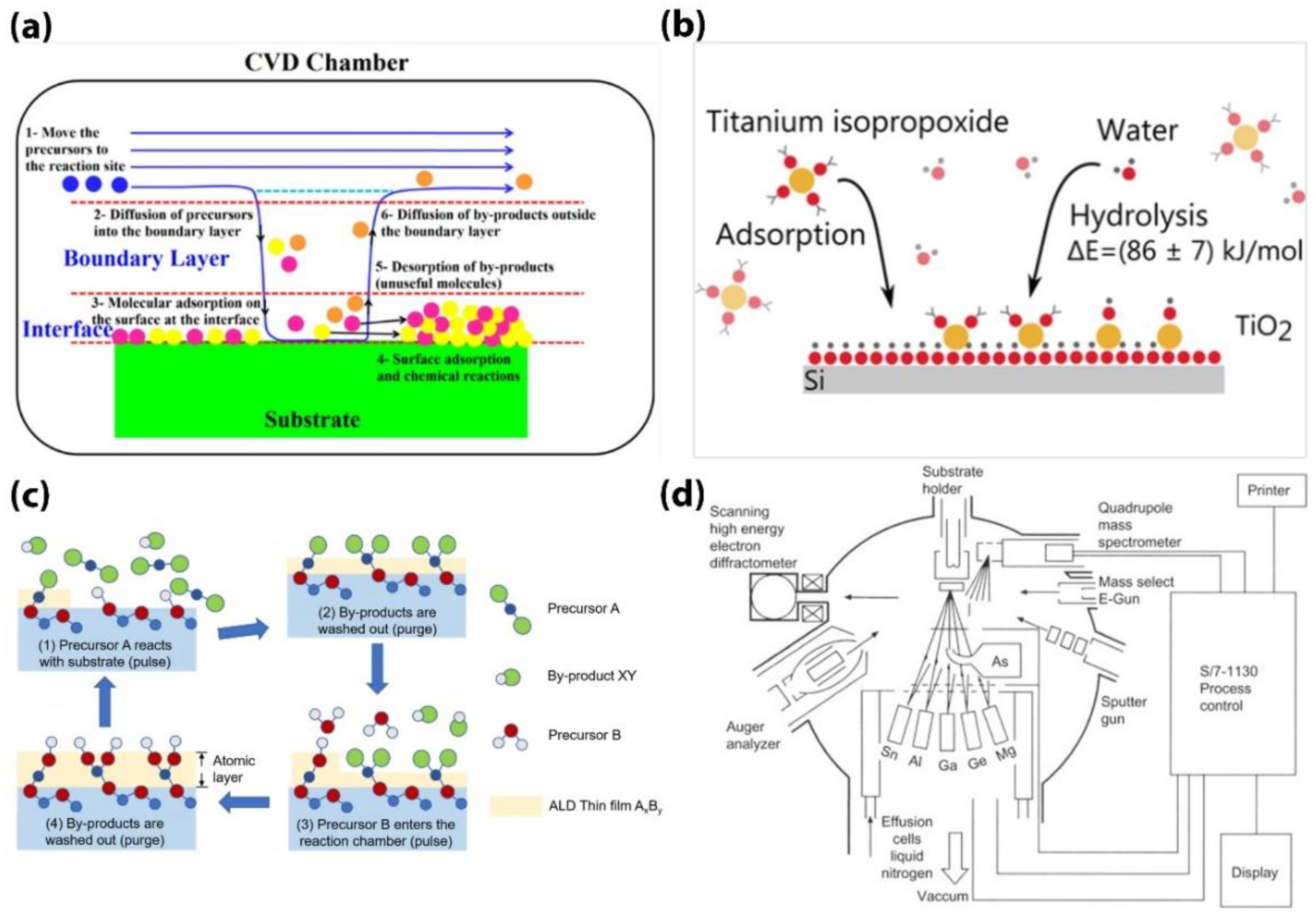
  87. M. Sabzi et al., “A Review on Sustainable Manufacturing of Ceramic-Based Thin Films by Chemical Vapor Deposition (CVD): Reactions Kinetics and the Deposition Mechanisms,” Coatings 2023, Vol. 13, Page 188, vol. 13, no. 1, p. 188, Jan. 2023. [CrossRef]
  88. M. Reinke, Y. Kuzminykh, and P. Hoffmann, “Low temperature chemical vapor deposition using atomic layer deposition chemistry,” Chemistry of Materials, vol. 27, no. 5, pp. 1604–1611, Mar. 2015. https:// 10.1021/CM504216P/ASSET/IMAGES/MEDIUM/CM-2014-04216P_0008.GIF.
  89. B. Yu, J. Zhang, Y. Yang, D. Yu, Y. Mai, and X. Chen, “Influences of deposition conditions on atomic layer deposition films for enhanced performance in perovskite solar cells,” Energy Mater 2024;4:400045., vol. 4, no. 4, p. N/A-N/A, May 2024. [CrossRef]
  90. H. Adachi and K. Wasa, “Thin Films and Nanomaterials,” Handbook of Sputter Deposition Technology: Fundamentals and Applications for Functional Thin Films, Nano-Materials and MEMS: Second Edition, pp. 3–39, Jan. 2012. [CrossRef]
  91. S. F. I. Abdillah, T. C. Kao, S. J. You, and Y. F. Wang, “Non-methane hydrocarbons from integrated semiconductor manufacturing processes: Assessments of chemical footprints, emissions factors, and treatment efficiency,” J Clean Prod, vol. 434, p. 140408, Jan. 2024. [CrossRef]
  92. Z. Luo, M. Gu, Q. Quan, Z. Jiang, and C. Wang, “Strategies for Managing Perfluorinated Compounds (PFCs) in Semiconductor Manufacturing: A Supply Chain and Public Management Approach,” Transactions on Engineering and Technology Research, vol. 2, pp. 76–85, Aug. 2024. [CrossRef]
  93. N. C. Obiuto et al., “Chemical management in electronics manufacturing: Protecting worker health and the environment,” https://wjarr.com/sites/default/files/WJARR-2024-0648.pdf, vol. 21, no. 3, pp. 010–018, Mar. 2024. [CrossRef]
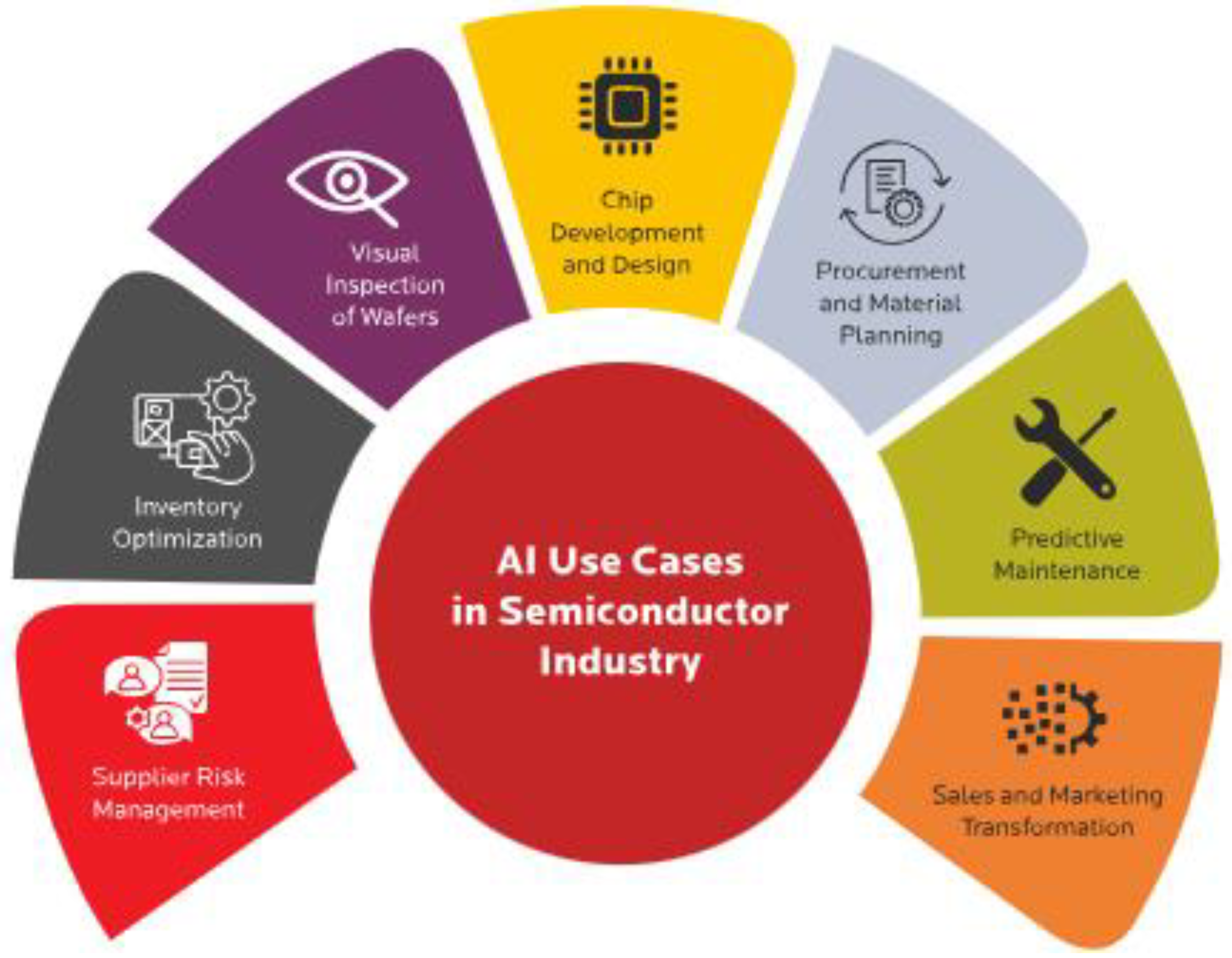
  94. A. Matin, M. R. Islam, X. Wang, H. Huo, and G. Xu, “AIoT for sustainable manufacturing: Overview, challenges, and opportunities,” Internet of Things, vol. 24, p. 100901, Dec. 2023. [CrossRef]
  95. D. D. W. Praveenraj, T. Vijayaraj, K. S. Kumar, N. K. Sakthivel, F. Multani, and P. Nagaveni, “Advanced Technological Improvements in Making of Smart Production Using AI and ML,” 2024 4th International Conference on Advance Computing and Innovative Technologies in Engineering, ICACITE 2024, pp. 178–183, 2024. [CrossRef]
  96. R. Alfred, N. Chinthamu, T. Jayanthy, E. Muniyandy, T. K. Dhiman, and T. Nimmy John, “Implementation of advanced techniques in production and manufacturing sectors through support vector machine algorithm with embedded system,” Measurement: Sensors, vol. 33, p. 101119, Jun. 2024. [CrossRef]
  97. P. Bhambri, S. Rani, and A. Khang, “AI-driven Digital Twin and Resource Optimization in Industry 4.0 Ecosystem,” Intelligent Techniques for Predictive Data Analytics, pp. 47–69, Sep. 2024. [CrossRef]
  98. M. Todescato et al., “Sustainable manufacturing through application of reconfigurable and intelligent systems in production processes: a system perspective,” Scientific Reports 2023 13:1, vol. 13, no. 1, pp. 1–13, Dec. 2023. [CrossRef]
  99. “How is AI Transforming the Semiconductor Industry- Birlasoft.” Accessed: Sep. 24, 2024. [Online]. Available: https://www.birlasoft.com/articles/ai-semiconductor-industry-use-cases-and-benefits.
  100. Y. Yu, D. Ma, and Y. Wang, “Structural resilience evolution and vulnerability assessment of semiconductor materials supply network in the global semiconductor industry,” Int J Prod Econ, vol. 270, p. 109172, Apr. 2024. [CrossRef]
  101. M. Zhang, W. Yang, Z. Zhao, S. Wang, and G. Q. Huang, “Do fairness concerns matter for ESG decision-making? Strategic interactions in digital twin-enabled sustainable semiconductor supply chain,” Int J Prod Econ, vol. 276, p. 109370, Oct. 2024. [CrossRef]
  102. P. O. Paul, J. O. Ogugua, and N. L. Eyo-Udo, “Sustainable procurement practices: Balancing compliance, ethics, and cost-effectiveness,” International Journal of Scientific Research Updates, vol. 8, no. 1, pp. 027–036, Jul. 2024. [CrossRef]
  103. D. Artudean, N. Aitonean, M. Parcalab, D. C. Popa, and L. Szabo, “Strategic Resource Challenges in the Development of Smart Cities,” 2024 24th IEEE International Conference on Automation, Quality and Testing, Robotics, AQTR 2024 - Proceedings, 2024. [CrossRef]
  104. Y. M. Ogunsuji, O. R. Amosu, D. Choubey, B. E. Abikoye, P. Kumar, and S. C. Umeorah, “Sourcing renewable energy components: building resilient supply chains, reducing dependence on foreign suppliers, and enhancing energy security,” https://wjarr.com/sites/default/files/WJARR-2024-2297.pdf, vol. 23, no. 2, pp. 251–262, Aug. 2024. [CrossRef]
  105. T. Ala-Lahti, “The awkward relations between EU innovation policies and environmental law,” Rev Eur Comp Int Environ Law, 2024. [CrossRef]
  106. “Creating Future-Ready Devices with SiC and GaN - Power Electronics News.” Accessed: Sep. 23, 2024. [Online]. Available: https://www.powerelectronicsnews.com/creating-future-ready-devices-with-sic-and-gan/.
  107. 107. K.-Y. Lee, “Analysis of the various SiC power MOSFETs,” pp. 1–1, Jun. 2024. [CrossRef]
  108. F. Di Giovanni, “Silicon Carbide: Physics, Manufacturing, and Its Role in Large-Scale Vehicle Electrification,” Chips 2023, Vol. 2, Pages 209-222, vol. 2, no. 3, pp. 209–222, Sep. 2023. [CrossRef]
  109. H. Qamar and H. Qamar, “Performance Improvement of SiC Based Electric Vehicle Charger with an Advanced PWM Method,” 2024 IEEE 25th Workshop on Control and Modeling for Power Electronics, COMPEL 2024, 2024. [CrossRef]
  110. M. Di Paolo Emilio, “Silicon Carbide Devices,” pp. 143–163, 2024. [CrossRef]
  111. S. M. Shanbhag, S. B. Shenoy, A. Sahoo, V. Paquinadin, N. Sam K, and J. Bodireddy, “Design and Implementation of GaN-Based DC-DC Converter for Solar Application in a DC Microgrid,” 2024 International Conference on Signal Processing, Computation, Electronics, Power and Telecommunication, IConSCEPT 2024 - Proceedings, 2024. [CrossRef]
  112. A. Abu-Siada and S. M. Islam, “Applications of Power Electronics in Renewable Energy Systems,” Power Electronics Handbook, pp. 797–843, Jan. 2024. [CrossRef]
  113. M. Xiao, “Application of Power Electronics Technology in Renewable Energy Systems,” Stud Soc Sci Res, vol. 5, no. 2, p. 157, Jun. 2024. [CrossRef]
  114. T. Cheng, “Application of Power Electronics Converters in Renewable Energy,” Journal of Electronic Research and Application, vol. 8, no. 4, pp. 101–107, Aug. 2024. [CrossRef]
  115. O. A. Adenekan, C. Ezeigweneme, and E. G. Chukwurah, “Driving innovation in energy and telecommunications: next-generation energy storage and 5G technology for enhanced connectivity and energy solutions,” International Journal of Management & Entrepreneurship Research, vol. 6, no. 5, pp. 1581–1597, May 2024. [CrossRef]
  116. M. Akbari, R. Bolla, R. Bruschi, F. Davoli, C. Lombardo, and B. Siccardi, “A Monitoring, Observability and Analytics Framework to Improve the Sustainability of B5G Technologies,” 2024 IEEE International Conference on Communications Workshops (ICC Workshops), pp. 969–975, Jun. 2024. [CrossRef]
  117. D. Renga, M. Ni, M. A. Marsan, and M. Meo, “Network Sharing to Enable Sustainable Communications in the Era of 5G and beyond,” IEEE International Conference on Communications, pp. 2840–2846, 2024. [CrossRef]
  118. S. Cascino et al., “Innovative Solutions to Make Driving Safer, Greener and More Connected,” 2024 IEEE International Symposium on Measurements and Networking, M and N 2024 - Proceedings, 2024. [CrossRef]
  119. J. I. Davies, A. D. Johnson, R. I. Pelzel, M. D. Geen, A. M. Joel, and S. W. Lim, “MOVPE and its future production challenges,” J Cryst Growth, vol. 605, p. 127031, Mar. 2023. [CrossRef]
  120. L. Sadath, D. Mehrotra, and A. Kumar, “Scalability in Blockchain - Hyperledger Fabric and Hierarchical Model,” 2022 IEEE Global Conference on Computing, Power and Communication Technologies, GlobConPT 2022, 2022. [CrossRef]
  121. S. Mukherjee, D. Pal, A. Bhattacharyya, and S. Roy, “Future of the Semiconductor Industry,” Handbook of Semiconductors, pp. 359–374, Jul. 2024. [CrossRef]
  122. A. R. Ghasemi, A. Taimouri, and A. Sayadi, “The Prospects of Future Production: An Arena for Emerging New Strategies and Policies of Manufacturing–The Household Appliance Industry’s Review,” International Journal of Business and Management, vol. 12, no. 6, p. p203, May 2017. [CrossRef]
  123. B. Teixeira, A. Mateus, and M. C. Brito, “Challenges to the Implementation of a Large-Scale Green Hydrogen Economy: Raw Materials Requirements, Technological Drivers, and Energy Policy Tasks,” SSRN, May 2024. [CrossRef]
  124. C. W. Tan et al., “Toward Sustainable Ultrawide Bandgap van der Waals Materials: An ab initio Screening Effort,” Adv Funct Mater, vol. 34, no. 11, p. 2308679, Mar. 2024. [CrossRef]
  125. M. F. Ashby, “Materials and Sustainable Development, Second Edition,” Materials and Sustainable Development, Second Edition, pp. 1–565, Jan. 2023. [CrossRef]
  126. D. He, D. R. Keith, H. C. Kim, R. De Kleine, J. Anderson, and M. Doolan, “Materials Challenges in the Electric Vehicle Transition,” Environ Sci Technol, vol. 58, no. 28, pp. 12297–12303, Jul. 2024. https://doi.org/10.1021/ACS.EST.3C09042/SUPPL_FILE/ES3C09042_SI_001.PDF. [CrossRef]
  127. O. Oguntona, O. Akinradewo, O. Mokono, B. F. Ogunbayo, and C. Aigbavboa, “Limitations of Futuristic Building Materials for Achieving Sustainability in the Construction Industry,” Sustainable Construction in the Era of the Fourth Industrial Revolution, vol. 107, no. 107, 2023. [CrossRef]
  128. E. Tolusso, L. Mascheretti, and F. Marzullo, “Innovative Value Chains: Advancements in Critical Raw Materials Recovery from E-Waste for Europe’s Economic Resilience,” International Conference Electronics Goes Green 2024+: From Silicon to Sustainability, EGG 2024 - Proceedings, 2024. [CrossRef]
  129. S. Siddiqua, S. Das Kumar, C. N. Mulligan, and R. Haigh, “A Decade Review of Research Trends Using Waste Materials in the Building and Construction Industry: A Pathway towards a Circular Economy,” Waste 2023, Vol. 1, Pages 935-959, vol. 1, no. 4, pp. 935–959, Nov. 2023. [CrossRef]
  130. C. Okogwu et al., “EXPLORING THE INTEGRATION OF SUSTAINABLE MATERIALS IN SUPPLY CHAIN MANAGEMENT FOR ENVIRONMENTAL IMPACT,” Engineering Science & Technology Journal, vol. 4, no. 3, pp. 49–65, Sep. 2023. [CrossRef]
  131. D. Salazar, I. Yakoumis, M. L. Grilli, D. Salazar, I. Yakoumis, and M. L. Grilli, “Substitution and Recycling of Critical Raw Materials in Optoelectronic, Magnetic and Energy Devices III,” physica status solidi (a), vol. 219, no. 15, p. 2200259, Aug. 2022. [CrossRef]
  132. A. L. Malest and M. R. Gabor, “Critical Raw Material in Circular Economy Context for Europe: A Decision Tree and Two-Step Cluster Analysis Approach,” Lecture Notes in Networks and Systems, vol. 926 LNNS, pp. 375–388, 2024. [CrossRef]
  133. S. Toumi, “Characteristics and modeling of wide band gap (WBG) power semiconductor,” Power Electronics for Next-Generation Drives and Energy Systems: Converters and control for drives, pp. 1–40, Jan. 2022. [CrossRef]
  134. J. V. Suman, A. S. Priya, G. M. A. Priyadarshini, K. Krishnamraju, A. Gangadhar, and M. Hema, “Integration Challenges and Opportunities for Gate-All-Around FET (GAA FET) in Next-Generation Electronic Devices,” vol. 112, pp. 1361–1368, Jul. 2024. [CrossRef]
  135. E. Chery, C. Fohn, J. De Messemaeker, and E. Beyne, “(Invited) Reliability Challenges in Advanced 3D Technologies,” ECS Meeting Abstracts, vol. MA2023-02, no. 17, p. 1188, Dec. 2023. [CrossRef]
  136. C. Zhang, X. Yuan, J. Wang, B. Hu, X. Yin, and Z. J. Shen, “Optimization of Power Sharing and Switching Frequency in Si/WBG Hybrid Half-Bridge Converters Using Power Loss Models,” IEEE J Emerg Sel Top Power Electron, vol. 11, no. 3, pp. 2837–2849, Jun. 2023. [CrossRef]
  137. X. H. Luo, X. Cheng, Y. B. Rao, J. A. Han, X. J. Deng, and B. Bin Cheng, “A W-band Hybrid Vector-modulated and Reflective-type Phase Shifter in 130-nm SiGe BiCMOS,” 2024 Photonics and Electromagnetics Research Symposium, PIERS 2024 - Proceedings, 2024. [CrossRef]
  138. J. L. Lyons, D. Wickramaratne, and A. Janotti, “Dopants and defects in ultra-wide bandgap semiconductors,” Curr Opin Solid State Mater Sci, vol. 30, p. 101148, Jun. 2024. [CrossRef]
  139. M. A. Porter, Y. Ma, Y. Qin, and Y. Zhang, “P-Type Doping Control of Magnetron Sputtered NiO for High Voltage UWBG Device Structures,” 2023 IEEE 10th Workshop on Wide Bandgap Power Devices and Applications, WiPDA 2023, 2023. [CrossRef]
  140. K. Fu, “(Invited) Wide Bandgap Semiconductor Homo- and Hetero-P-N Junctions,” ECS Meeting Abstracts, vol. MA2024-01, no. 32, p. 1576, Aug. 2024. [CrossRef]
  141. L. Voss, “(Invited) Wbg and Uwbg Photoconductors and Applications,” ECS Meeting Abstracts, vol. MA2024-01, no. 32, p. 1566, Aug. 2024. [CrossRef]
  142. Y. Song and Y. Dong, “Influence of resource compensation and complete information on green sustainability of semiconductor supply chains,” Int J Prod Econ, vol. 271, p. 109227, May 2024. [CrossRef]
Figure 1. (a) Bandgap Energy Comparison of Semiconductor Materials (Silicon, SiC, GaN) (b) Breakdown Strength Comparison of Semiconductor Materials (Silicon, SiC, GaN).
Preprints 140636 g001
Figure 2. (a) Semiconductor Market Share by Region in 2023 (%). (b) Projected Semiconductor Market Size in the Asia Pacific Region from 2023 to 2033 (USD Billion). (c) Semiconductor Market Share by Application in 2023 (%). (d) Projected Global Semiconductor Market Size from 2023 to 2033 (USD Billion). Source: Precedence Research [18].
Preprints 140636 g002
Figure 3. Material Properties of WBG semiconductors (SiC, GaN) compared to Si presented in a spider chart.
Preprints 140636 g003
Figure 4. Timeline of the most important historical milestones throughout the last centuries [51].
Preprints 140636 g004
Figure 5. (a) Schematic of the main steps of the CVD process [87]. (b) Schematic Diagram of ALD type reaction to a high Vacuum Low-temperature CVD process [88]. (c) The reaction process of ALD [89]. (d) Typical MBE system [90].
Preprints 140636 g005
Figure 6. AI use cases in semiconductor industry. (Source: birlasoft [99]).
Preprints 140636 g006
Figure 7. Si, SiC, and GaN opportunities (Source: Power Electronics News) [106].
Preprints 140636 g007
Table 2. Sustainability strategies in WBG semiconductor manufacturing, emphasizing their contributions to various environmental factors.
Sustainability Practice Description Impact on Recycling Impact on Energy Consumption Impact on Waste Reduction Toxic By-product Elimination
Low-Energy Epitaxial Growth Reduces energy required in the deposition of semiconductors Low High Moderate Moderate
Green Chemistry in Manufacturing Utilizes environmentally friendly chemicals to replace harmful substances in production processes Low Moderate High High
Closed-Loop Recycling Systems Recovers and reuses materials from semiconductor production waste (e.g., silicon wafers, gallium). High Low High Moderate
Reduction of Chemical Vapor Deposition (CVD) Innovating CVD processes to minimize toxic emissions and lower energy demands Low High Low High
Recycling of Semiconductor Materials Implements strategies for reclaiming materials like silicon carbide (SiC) and gallium nitride (GaN) High Low High Low
Advanced Wastewater Treatment Integrates new filtration technologies to treat and reuse wastewater from production facilities Low Low High High
Energy Efficiency Measures Incorporates energy-efficient equipment and renewable energy sources to power semiconductor production lines Low High Moderate Low
Disclaimer/Publisher’s Note: The statements, opinions and data contained in all publications are solely those of the individual author(s) and contributor(s) and not of MDPI and/or the editor(s). MDPI and/or the editor(s) disclaim responsibility for any injury to people or property resulting from any ideas, methods, instructions or products referred to in the content.
Copyright: This open access article is published under a Creative Commons CC BY 4.0 license, which permit the free download, distribution, and reuse, provided that the author and preprint are cited in any reuse.
Prerpints.org logo

Preprints.org is a free preprint server supported by MDPI in Basel, Switzerland.

Subscribe

Disclaimer

Terms of Use

Privacy Policy

Privacy Settings

© 2025 MDPI (Basel, Switzerland) unless otherwise stated