
Submitted:
23 January 2026
Posted:
03 February 2026
You are already at the latest version
Abstract
Deposition of amorphous B (a-B) onto Si substrates via chemical decomposition of B2H6 molecules produces a-B/Si heterojunctions which are the core parts of photodetectors used in vacuum ultraviolet (VUV) and potentially in extreme ultraviolet (EUV) lithog-raphy. However, fundamental questions regarding the limit on the thickness of the de-posited a-B thin-films and the intrinsic electronic nature of the B atoms adjacent to the Si substrate remain unanswered. Here we investigated the local structural and electronic properties of atomic-thin amorphous boron (a-B) layers at the Si{001} substrates using ab initio molecular dynamics (AIMD) techniques. The investigation revealed a rich variety of local chemical bonding and consequently interfacial electronic properties. For thin a-B layer(s)/Si systems, most of the a-B atoms at the interface formed (-B-Si-B-Si-) chains on the Si{001} surface, occupying the positions of the missing Si atoms and strongly hy-bridizing with the nearby Si atoms. Localized defect states at the Fermi level for the in-terfacial Si and B atoms were found in the pseudo-gap. These states have a major influ-ence on the electrical properties of the device. The predicted minimum thickness of the a-B films is 1nm, a useful metric for the manufacturing of a-B/Si devices. The information obtained here further helps understanding the working mechanisms of a-B/Si interfaces for photon detection, and constructing new core devices for potential applications in the field of metal/semiconductor heterojunctions for photodetection, photovoltaics, Schottky diodes and semiconductor devices.
Keywords:
Ab Initio molecular dynamics
; ultraviolet photodiode
; thin layer
; PureB devices
; interface chemistry
1. Introduction
In recent years, the semiconductor industry has steadily been moving on from the 193 nm-based Deep Ultraviolet (DUV) lithography technology towards the EUV (Extreme Ultraviolet, 13.5 nm wavelength) spectrum to reach smaller node sizes. However, development of a new generation of photolithography devices capable of detecting photons at these wavelengths is dependent on the ability to detect EUV photons. The amorphous Boron (a-B) on Silicon (a-B/Si) photodiode has been known to be a good detector for both DUV and EUV photons due to the shallow depletion region and nanometer-thin—or even atomic-thin, capping boron layer. Experiments have revealed that these devices are able to reach a quantum efficiency of approximately 46% when used to detect 193 nm wavelength photons, while at 13.5 nm the device approaches the theoretical limit (Sarubbi, Nanver, & Scholtes, CVD delta-doped Boron surface layers for ultra-shallow junction formation, 2006; Sarubbi F. , Nanver, Scholtes, Nihtianov, & Scholze, 2008; Mohammadi, de Boer, & Nanver, Temperature dependence of chemical-vapor deposition of pure boron layers from diborane, 2012; Sberna, Fang, Fang, & Nihtianov, 2021). The a-B/Si device is furthermore shown to be stable under prolonged exposure to UV photons and low-energy electrons as well as environmental factors such as temperature (Sberna, Fang, Fang, & Nihtianov, 2021). As a result, the a-B/Si photodiodes compare very favorably to commercially available Si-based VUV and EUV (Sarubbi F. , Nanver, Scholtes, Nihtianov, & Scholze, 2008; Sberna, Fang, Fang, & Nihtianov, 2021) and are already used in nanolithography devices. In the interest of further development, studying the fundamental properties, e.g. the limit of the thickness of the deposited a-B layer and local structural and electronic properties, is necessary to reach the level of comprehensive understanding needed to obtain devices with more desirable properties.
Experimental efforts on the a-B/Si photodiodes have been primarily focused on the creation process, through experimentation with the deposition temperatures (Mohammadi, de Boer, & Nanver, Temperature dependence of chemical-vapor deposition of pure boron layers from diborane, 2012; Knezevic, Liu, Hardeveld, Suligoj, & Nanver, 2019), thickness (Knezevic, Liu, Hardeveld, Suligoj, & Nanver, 2019) and other conditions such as oxidation at the interfaces (Mohammadi V. , de Boer, Scholtes, & Nanver, 2013), as well as electric and optoelectronic properties measurements (Sberna, Fang, Fang, & Nihtianov, 2021). Recently, High-Resolution Transmission Electron Microscopy (HR-TEM) measurements provide clarity on the local structure of the a-B/Si heterojunction—specifically, the observed sharp interface that arises at low deposition temperatures (400 °C)—did not fit a δ-doping model (Mohammadi, Nihtianov, & Fang, A doping-less junction-formation mechanism between n-Silicon and an atomically thin Boron layer, 2017; Fang & Nihtianov, A Comparative Analysis of the Junction Formation Mechanisms of the Boron on Silicon Junction, 2024) as this model relies on diffusion of B atoms, which requires higher temperatures due to the relatively high kinetic barrier (Mohammadi, Nihtianov, & Fang, A doping-less junction-formation mechanism between n-Silicon and an atomically thin Boron layer, 2017). These findings indicate a need to build a new model to explain the electronic properties of this heterojunction. However, the obtained information about local structures and B distribution via the HR-TEM images is ‘averaged’ over the thickness of the TEM samples; Information on the local structures, chemical interactions and limits of a-B thickness on the electronic properties of the a-B/Si interfaces at an atomic level is necessary to understand the interface in a better and more comprehensive way.
Theoretical approaches, especially parameter-free first-principles methods are very useful to describe such systems at the required scale. Theoretical efforts were made to study the chemical processes involved in the chemical decomposition of the B2H6 precursor, which has up until now yielded constructive information on the formation of B layers on Si at an atomic scale in addition to its electrical properties (Fang, Mohammadi, Nihtianov, & Sluiter, Stability, local structure and electronic properties of borane radicals on the Si(1 0 0) 2 × 1:H surface: A first-principles study, 2017; Fang, Mohammadi, Nihtianov, & Sluiter, Stability, geometry and electronic properties of BH_n (n = 0 to 3) radicals on the Si0 0 1 3×1:H surface from first-principles, 2020). It was found that the deposited B atoms and BHn (n = 1 to 3) radicals introduce localized surface states which affect the electronic properties of these interfaces. Recent first-principles modelling has provided detailed information about the local structures and interfacial interactions, as well as electronic properties of an a-B bulk on Si heterojunction (Fang, Nihtianov, Sberna, & Fang, Interfaces between crystalline Si and amorphous B: Interfacial interactions and charge barriers, 2021). Of particular interest is the local structure and ordering of the B atoms on top of the Si surface, as it was shown that certain coordination patterns (1 and 2 B atoms per Si atom for the {111} and {001} surfaces, respectively) are dominant at the interface. This observation has led to questions about the conditions under which these local chemical bonds are found, particularly whether this is a consequence of the thickness of the amorphous boron (a-B) layer and how this influences the electronic properties of the interfaces, in addition to the intrinsic electronic nature of the a-B atoms adjacent to the Si substrates.
Here we systematically analyze the effects of the thickness of amorphous B (from one to four atomic layers) on the local structural and electronic properties of the a-B/Si{001} systems using an ab initio molecular dynamics approach. We show the growth and structure of the heterojunction using a first principles approach and find the local ordering of B near the interface. We further discuss the effects of the low B atom population on the condensation of an interfacial layer and compare the electronic properties of this interface to the bulk growth process of amorphous B. The knowledge obtained here regarding the growth mechanism of bulk B and the electronic properties is further applicable to the metal/semiconductor heterojunctions in general for various applications including photon detection, photovoltaics, Schottky diodes and semiconductor devices (Sberna, Fang, Fang, & Nihtianov, 2021; Zhu, Wen, Xiong, Wei, & Wang, 2025; Zhao, et al., 2025; Ghosh, Weoi, Islam, & Ghosh, 2018; Fang, Nihtianov, Sberna, de Wijs, & Fang, Interfacial charge transfer and Schottky barriers at c-Si/a-In heterojunctions, 2022; Nicholls, 2021).
2. Simulation Methods
2.1. The a-B/Si{001} Interface Systems
To study the properties of an ideal a-B/c-Si system, we simulated the interface at the atomic scale using AIMD simulation techniques. We first individually built the components of the interfaces which consist of the crystalline Si(001) surface and the amorphous B slabs of various atomic thicknesses. We started from a bulk a-B/Si{001} interface system which has a tetragonal cell with an in-plane axis a = 3a0 (where a0 is the lattice parameter of the Si cell with consideration of thermal expansion) (Arblaster, 2018; Watanabe, Yamada, & Okaji, 2004).
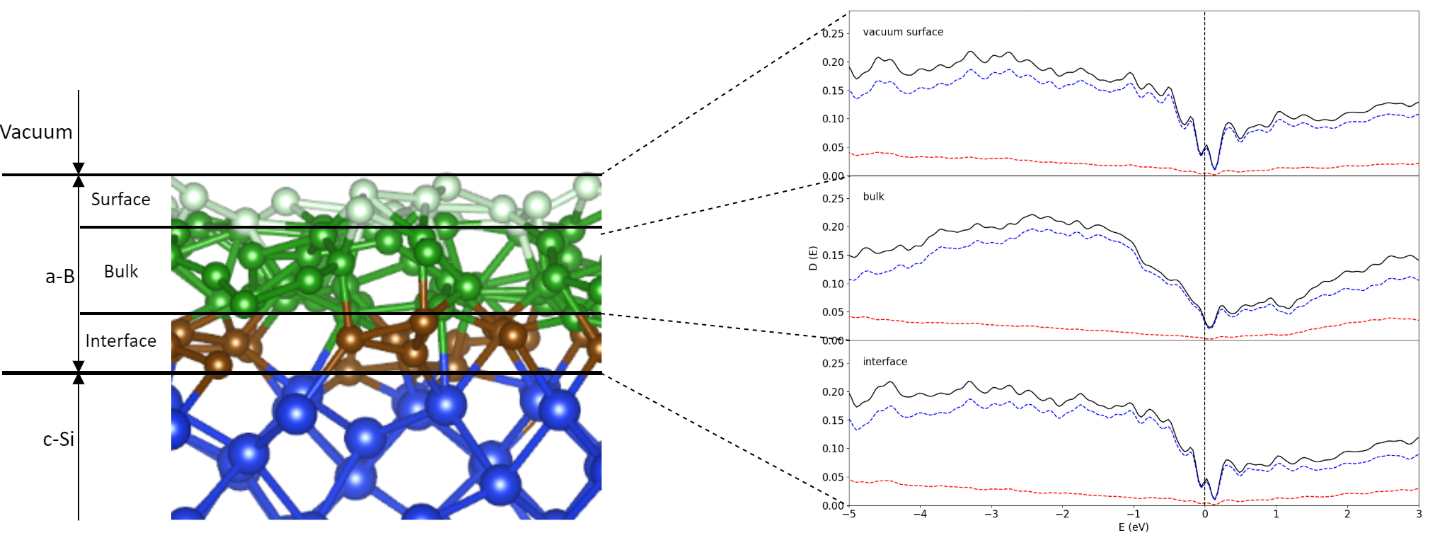
To independently obtain an amorphous B system, we simulated the heating of a pure B system at 4000 K, which is above the melting point of B of 2348 K. This was left to run for 2000 steps at 1.5 fs per step or 3.0 ps in total, before cooling the system to 1000 K in 4.5 ps. A similar method was used in our prior work to create bulk a-B (Fang, Nihtianov, Sberna, & Fang, Interfaces between crystalline Si and amorphous B: Interfacial interactions and charge barriers, 2021). This slab of a-B was then placed on top of the Si crystal in a supercell. The length of the c-axis for this supercell was determined by the thickness of the Si-slab and the a-B layer. Thus, a tetragonal supercell with a = 16.40 Å, c = 19.19 Å was built. This cell contains eight atomic layers of Si (144 Si atoms) and an a-B layer of 300 B atoms. The built bulk a-B/Si{001} interface system was modelled via an AIMD simulation at 1000 K for 2000 steps with the substrate Si atoms being pinned. A cross-section of the equilibrated a-B/Si{001} interface system is shown in Figure 1a.
To create atomic-thin a-B layers, the excess a-B atoms were removed in the bulk a-B/Si{001} interface system. Three atomic-thin a-B/Si{001} interface systems were built (see Figure 1) which we indicate as BX/Si144 (X = 25, 50 or 100). The obtained systems retain the tetragonal cell with a = 16.40 Å, c = 34.18 Å. With these changes we obtained four a-B/Si{001} interfaces with thin a-B layers with one, two and four a-B layers on the Si substrates (Figure 1b-d, respectively). The vacuum length between the B layers for each system is longer than 15.2 Å. This separation helps with avoiding unphysical interactions between the two interfaces in these systems.
2.2. Ab Initio Techniques
In this study, we employed the first-principles software VASP (Vienna Ab initio Simulation Package) (Kresse & Hafner, 1994; Kresse & Furthmüller, 1996) to simulate the a-B/Si interfaces. The VASP framework utilizes a pseudopotential plane-wave approach within the density functional theory (Hohenberg & Kohn, 1964) with the projector augmented wave scheme (Blöchl, 1994). The generalized gradient approximation with the scalar relativistic approximation by Perdew, Burke and Ernzerhof (GGA-PBE) was used for the exchange and correlation terms (Perdew, Burke, & Ernzerhof, 1996).
We used a cut-off energy of 400.0 eV for the wave functions and 550.0 eV for the augmentation functions, respectively for the duration of the structure relaxation process. These cut-off energies are higher than the corresponding default values of the atoms (EMAX/EAUG=245.3 eV/322.1 eV for Si and 318.6 eV/535.5 eV for B). Dense k-meshes were employed, e.g. 8×8×1 (32 to 34 k-points), generated using the Monkhorst-Pack scheme for the Brillouin zones of the interface systems (Monkhorst & Pack, 1976).
For the AIMD simulations, a cut-off energy of 320 eV and the Г (0,0,0) point in the Brillouin zone were used since there is a lack of translational symmetry in the systems with amorphous B layers. The obtained interface systems were simulated at 1000K for two to five ps (picoseconds). The ab initio molecular dynamics simulations showed that the interface systems reached equilibrium at about 0.5 ps as shown in Figure 2b for the one a-B layer system as example. The equilibrated systems were then used for further first-principles band structure calculations and local structural analysis.
3. Results
3.1. Elemental Solids of Solids α-B, Si and Amorphous B (a-B)
In order to make a direct comparison between the properties of B in its crystalline and amorphous form, we first calculated the electronic properties of the elemental solids α- phase (α-B) and amorphous B in an approach which was similarly used in our prior work (Fang, Nihtianov, Sberna, & Fang, Interfaces between crystalline Si and amorphous B: Interfacial interactions and charge barriers, 2021). The structure of α-B is well-studied and is characterized as a rhombohedral lattice with space group R-3m (Number 166) which contains two groups of B atoms and 12 B atom in total (α-B12) (Decker & Kasper, 1959). The boron atoms in the α-B12 system have six to seven neighbors with interatomic distances ranging from 1.71 to 2.02 Å. The calculated partial Density of States (pDOS) of the two different species in α-B12 are shown in Figure 3.
The band structure of α-B12 consists of two parts, a valence band from -10.1 eV to the Fermi level, which we set to 0 eV, and a conduction band from +1.7 eV and above. The 2s states dominate the lower part of the valence band from -10.1 eV to -8.0 eV, while the upper part of the valence band and the conduction band are strongly characterized by the 2p states. A band gap is found for the α-phase as shown in Figure 3 of approximately 1.2 eV which is smaller than the experimental value (1.7 eV) (Bullett, 1982). The underestimation of band gaps for semiconducting materials is a known factor for density-functional theory methods (Jones, 2015). Analysis shows that the occupied states near the Fermi Level are predominantly B 2p states, with moderate contribution from the s-orbitals.
The amorphous B system has, by definition, no clear translational symmetry. Qualitatively, local structures are found within the system in the form of distorted B12 clusters. For a-B there is no clear band gap, as evident from Figure 4, despite the presence of distorted B12 clusters in the sample. Furthermore, the total DOS (tDOS) of amorphous B (300 atoms) in Figure 4 shows that the Fermi level falls in a valley with has localized defect states. By breaking the symmetry and effectively introducing numerous defects, the bandgap which was opened in the α-B12 system is filled with defect states. This leads to the ‘bad’ metal nature of bulk a-B as confirmed in previous calculations (Fang, Nihtianov, Sberna, & Fang, Interfaces between crystalline Si and amorphous B: Interfacial interactions and charge barriers, 2021).
Finally, to complete the comparison, we simulated crystalline Si. The structure of Si is very well-studied and consists of a face-centered cubic (fcc) lattice (space group Fd-3m, nr. 227) with Si atoms at the (0, 0, 0) and (¼, ¼, ¼) Wyckoff sites. From our structure optimization we produced a lattice parameter of 5.468 Å for Si. This agrees well with the experimental value (5.4298 Å at 0 K) (Arblaster, 2018). The calculated band gap is 0.7 eV which is lower than the experimental value (1.17eV) (Bludau, Onton, & Heinke, 1974). The underestimation of band gaps for Si has been widely reported for the DFT-GGA approaches (Fang, Nihtianov, Sberna, & Fang, Interfaces between crystalline Si and amorphous B: Interfacial interactions and charge barriers, 2021; Perdew, Burke, & Ernzerhof, 1996; Jones, 2015).
3.2. Local Structures at the a-B/Si{001} Interfaces
Using the parameters and input systems as described in Section 2 we performed ab initio molecular dynamics simulations for the c-Si/a-B interface systems of different a-B thickness. Cross-section views of the thermally equilibrated systems are shown in Figure 5a-f in the Si(001) and Si(110) directions. Furthermore, the various local a-B/Si configurations present in these systems are drawn in Figure 5g-j.
At the bulk a-B/Si{001} interfaces, the Si atoms generally maintain the crystalline structure at the interface while no ordering is found for the B atoms within the bulk of B away from the interface (Figure 1a). However, a slight distortion of the Si crystalline lattice takes place at the surface. This is likely due to a combination of factors: Edge effects from the discontinuation of the lattice, and the presence of the B atoms causing a reconstruction of the Si surface, as well as kinetic effects (Fang, Mohammadi, Nihtianov, & Sluiter, Stability, local structure and electronic properties of borane radicals on the Si(1 0 0) 2 × 1:H surface: A first-principles study, 2017; Fang, Mohammadi, Nihtianov, & Sluiter, Stability, geometry and electronic properties of BH_n (n = 0 to 3) radicals on the Si0 0 1 3×1:H surface from first-principles, 2020; Alerhand & Mele, 1987; Weakliem & Carter, 1992). The B atoms adjacent to the Si substrates appear to conform to the Si(001) crystal, by occupying the vacant sites that would have been occupied by Si. The thickness of the B layer on top grows with the quantity of B atoms, which is to be expected of atoms condensing on a surface.
Figure 5a and Figure 5d show the structure and coordination of the interfacial atoms for the B25/Si system. The maximum length of the drawn a-B/Si bonds was chosen to be 2.2 Å based on the covalent radii of the Si and B atoms (1.11 Å and 0.82 Å respectively (Brown, 2009)) with an additional 10% margin to consider the contribution to the chemical bonding according to the valence bond theory (Brown, 2009). Most of the B atoms are positioned near the original crystalline Si positions. The interfacial Si atoms primarily have two B neighbors and form (-B-Si-B-Si-) chains (Figure 5j). Thus, most B atoms have just two Si neighbors. This is similar to the previously modelled reconstructed Si{001} surfaces with BHn radicals (Fang, Mohammadi, Nihtianov, & Sluiter, Stability, local structure and electronic properties of borane radicals on the Si(1 0 0) 2 × 1:H surface: A first-principles study, 2017; Fang, Mohammadi, Nihtianov, & Sluiter, Stability, geometry and electronic properties of BH_n (n = 0 to 3) radicals on the Si0 0 1 3×1:H surface from first-principles, 2020). Given the thinness of the B layer in this system, bulk B structures were not expected to form and were not found. Furthermore, Figure 5a also shows that the AIMD simulations resulted some B atoms moving away from the Si surface, forming B islands. This may help understand the island growth of a-B at the Si substrates.
Increasing the thickness of a-B led to more neighbors for the interfacial Si and the B atoms adjacent to the Si substrates Figure 5b, c, e and f. Analysis revealed that the Si surfaces become less distorted with increasing a-B thickness, which also changes their chemical bonding and related electronic properties. The well-known formation of the B12 icosahedral clusters was not observed in the simulated systems of one or two atomic-thin a-B layers. However, smaller clusters were found for the B100/Si system with four a-B layers, indicating the preference for the B atoms cluster, , which was not present for the B25/Si and Bi50/Si configurations. This is likely due to the Si-B interactions dictating the composition of the B layer. In other words, the direct interaction between Si and B atoms at the interface leads to a more favorable configuration in comparison to the B-B bonds. This is contrary to the expectation of B12 cluster formation in amorphous B bulks, as found in literature (Kuhlmann, Werheit, Lundström, & Robers, 1994).
The preference for the Si-B interactions is additionally reflected in the coordination of interfacial B atoms. We define the coverage of the Si layer as the percentage of surface Si atoms interfacing with the number of a-B atoms. The coverage of the interfacial Si atom layers by B atoms for each of the BX/Si144 system is shown in Figure 6. Here we find that the coverage is maximal even for the 25 B atom system. Every surface Si atom has formed a bond with one or more B atoms in the case of the 25- and 50-B atom systems, and only a single Si atom in the B100/Si144 system was found with no Si-B bonds.
The distributions of B coordination numbers in Figure 6 correspond to the local structures shown in Figure 5g-i. The B atoms were found predominantly in the 1 Si to 2 B atoms (1Si:2B) configuration shown in Figure 5h. These atoms formed a zigzag pattern as drawn in Figure 5j on all three interfaces. To some extent, the Si-B interactions lead to an extension of the Si crystalline structure into the first B layer in the simulated systems. This has a profound effect on the electronic properties of the heterojunction as the electronic properties of B and Si share strong similarities. However, note that the amount of B atoms increases and the amount of Si atoms remain the same; The ratio between the amount of 1Si:1B and 1Si:2B clusters changes only slightly between the increase in B atoms between the BX/Si144 systems. The largest change was found between the B25/Si144 and B50/Si144 interfaces as the distribution of coordination shifts even more towards the 1Si:2B configuration (Figure 6b) due to the second layer of B providing a different environment. In particular, the interface atoms are shielded from the vacuum with the addition of the second layer. This increase corresponds to more and more B atoms being included in the a-B bulk, which logically means that the electronic properties of the interface were increasingly determined by a-B.
In brief, the B atoms interacting with Si showed a preference for the original high-symmetry positions, which relates to the crystal field of the surficial Si atoms, as shown in Figure 5d-f. These atoms tended towards settling in the planes between the interfacial Si atoms. Additionally, dual occupation of these positions was made possible by the small size of B atoms relative to Si. The repulsive charge interaction between the two B atoms was partially negated by the attractive force of the nearby Si atoms in this configuration. This becomes more evident once more B atoms were added, resulting in an increased amount of such B atoms sharing high symmetry points in the B50/Si144 and B100/Si144 systems compared to B25/Si144.
3.3. Electronic States at the a-B/Si Interfaces
The interactions between the Si and B atoms at the interface are expected to play a dominant role in determining the electronic properties at this interface. A graph of the partial density of states (pDOS) over the entire surface and for the individual species found near the B25/Si144 interface is shown in Figure 7. The localized states at the interface here were found within the bandgap of the Si and B structures. In effect, these states closed the bandgap which resulted in the formation of a pseudo-gap. The pDOS curves given in Figure 7a-b were averaged out over all the atoms in the entire system. However, the local interactions play a large role in the electronic properties.
Analysis of the eigenvectors near the Fermi level showed that the Si 3s 3p and the B 2s 2p states interact, which in turn is the cause of the bonding between Si and B at the interface. This is reflected in the local structures found in Section 3.2, as the Si crystalline structure partially extends past the interface into the first layer of B atoms. The orientational preference of these orbitals is partially responsible for the distribution of coordination numbers in Figure 6, as the Si atoms require 2 additional bonds at the interface.
The pDOS curves corresponding to the Si atoms in the Si-B configurations found in Figure 5g-i are shown in Figure 7c-e. There is a remarkable difference in DOS depending on whether the Si is coordinated with 1 or with 2, 3 B atoms. For the 1Si:2B cluster (Figure 5h) the bandgap in Figure 7d is pronounced though localized states have been introduced by the Si-B bonding. The 1Si:1B formation (Figure 5g and Figure 7c) has a larger number of states in general near the bandgap compared to 1Si:2B and 1Si:3B (Figure 5i and Figure 7e). The general outlines of each species of Si differ significantly, though all three clusters have an important element in common: A sharp localized peak right at the Fermi level. The 1Si:2B configuration is the most common one for the B25/Si144 system according to Figure 6 and therefore the pDOS in Figure 7d should primarily determine the average pDOS in Figure 7a, with a major contribution from the 1Si:1B pDOS (Figure 7c). The contribution from the 1Si:3B clusters in this system to the overall properties is very weak due to how few occurrences there are.
The pDOS for the B atoms given in Figure 7f-h shows that the bandgap is closed by localized states and that the Fermi level lands on top of a sharp peak for the B atoms as well. The valley is more prominent and shows that the bandgap is still maintained. A small majority of the B atoms end up in the 1B:2Si ratio, though this distribution is less skewed when compared to 2B:1Si for the Si distributions.
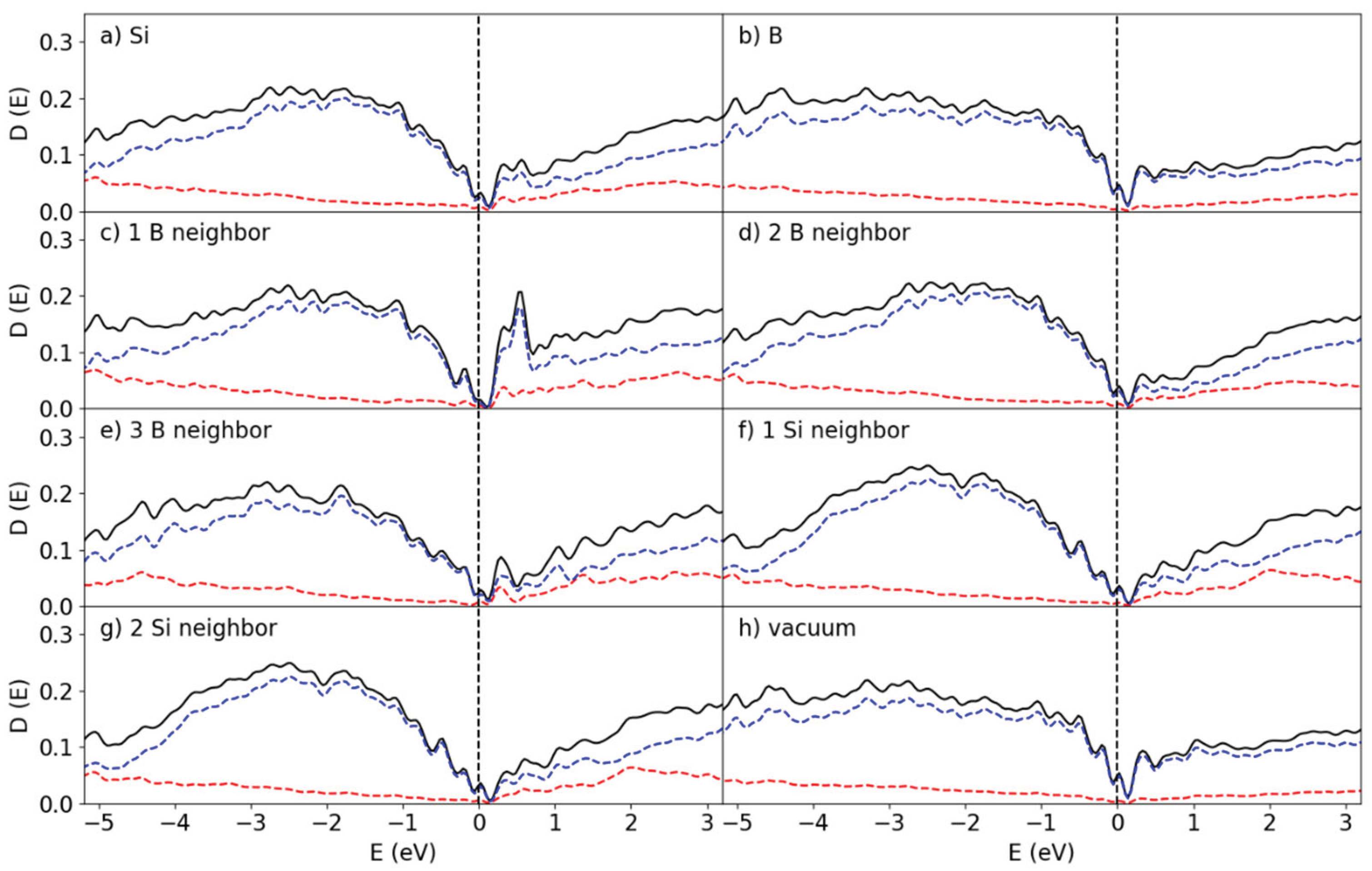
The DOS curves for the B50/Si144 interface as shown in Figure 8 resemble the ones for the B25/Si144 system. In both systems the band gaps disappear for the interfacial Si atoms and sharp peaks arise in place instead from the localized states created by the Si-B interaction. However, unlike the B25/Si144 system, the Fermi level of the B50/Si144 system does not lie directly on top of a peak for the 1Si:1B and 1Si:3B configurations and the height of the peaks are much smaller.
As the symmetry was broken in these systems, the splitting of the degenerate states in the B25/Si144 and B50/Si144 systems is unlikely to be caused by structural distortion (Jahn & Teller, 1937). This is more likely related to the low number of B atoms (Si-B-Si) chains. The peak at the Fermi level for the interfacial Si atoms comes from the B atoms with low numbers of chemical bonds as compared with that of bulk a-B (See Section 3.1).
Finally, the amount of B atoms was doubled again to create the B100/Si144 for which the DOS is shown in Figure 9. This doubling certainly did not double the amount of surface B with Si-B interactions but manifested the formation of extra layers on top of the B50/Si144 structure instead. This in turn has lead to an increased contribution to the DOS by the non-interface B, which partially corresponds to the B atoms interfacing with vacuum as found in Figure 9h. Aside from this effect, the B100/Si144 system differs from the previous two with the Fermi Level not landing directly on top of a peak, in addition to the associated peak being much smaller.
The bandgap is much more recognizable for this structure, though its width still remains significantly smaller than what is found for α-B12 and does not resemble the distribution found for B300. Instead, the electronic structure of this interface are closer to those found in a prior work for bulk a-B on Si{001} (Fang, Nihtianov, Sberna, & Fang, Interfaces between crystalline Si and amorphous B: Interfacial interactions and charge barriers, 2021). This is an indication that four layers of a-B already start to exhibit the bulk properties which, realistically, dominate experimental results on devices made with thicker a-B layers.
The surficial B atoms exposed to vacuum appear to exhibit semiconducting features. Experimental observation of the nature of a-B observe semiconductor properties for surficial a-B though the bulk should be considered a ‘bad metal’. This is due to the nature of photoemission spectroscopy as it is a surface-sensitive technique (Powell, Attenuation lengths of low-energy electrons in solids, 1974; Powell, Practical guide for inelastic mean free paths, effective attenuation lengths, mean escape depths, and information depths in x-ray photoelectron spectroscopy , 2020). The mean free path of electrons escaping from the solid is about 10 Å for photoelectrons with an energy from 20 eV to 1500 eV (Powell, Attenuation lengths of low-energy electrons in solids, 1974; Powell, Practical guide for inelastic mean free paths, effective attenuation lengths, mean escape depths, and information depths in x-ray photoelectron spectroscopy , 2020). Therefore, the bulk properties are hardly detected and these measuring techniques primarily find the edge effects, instead.
4. Discussion
The present ab initio molecular dynamics simulations revealed that the a-B atoms adjacent to the Si{001} substrates occupy the high symmetry sites of the missing Si atoms, extending the crystal structure of the Si substrates. However, the smaller B radius causes the interfacial Si and B atoms to form (-Si-B-Si-B) chains and the a-B atoms thus have dominantly two Si neighbors for the systems with one or two a-B layers. Electron band structure calculations showed that the high density of states–manifesting as sharp peaks–at the Fermi level for the interfacial Si and B atoms, indicating instability according to Stoner’s criteria (Stoner, 1937). Consequently, the a-B atoms tend to form islands.
Our simulated process is different from chemical vapor deposition which takes place in N2-filled reaction chambers while diborane, B2H6, is introduced with an inert carrier gas. Prior theoretical work has shown that B2H6 decomposes into two BH3 radicals and interacts with the hydrogen-passivated Si surface, forming Si-H-BH3 clusters which further decompose into BHn and H2 until only Si-B is left (Fang, Mohammadi, Nihtianov, & Sluiter, Stability, local structure and electronic properties of borane radicals on the Si(1 0 0) 2 × 1:H surface: A first-principles study, 2017; Fang, Mohammadi, Nihtianov, & Sluiter, Stability, geometry and electronic properties of BH_n (n = 0 to 3) radicals on the Si0 0 1 3×1:H surface from first-principles, 2020). We posit that the following interactions prevent doping and create a sharp interface:
- The larger BHn (n = 1 to 3) radicals require high kinetic energies to penetrate into the bulk of Si.
- The reaction between BHn and the H atoms on the surface of Si limits the kinetic energy of the radical by acting as a soft landing regardless of the deposition temperature.
- The bond between Si and B atoms is very strong and prevents further movement of the B atoms after the deposition process.
- The kinetic energies of the BHn radicals are limited at low temperatures and are not enough to overcome the relatively high diffusion barriers.
In the end, the resulting B layer majorly stayed on top of the Si surface such as found using HR-TEM imaging from samples prepared at low temperatures [7]. The interface interactions are then primarily responsible for the electronic properties of this system as previously predicted [11]. Therefore, we may be able to exclude the possibility of δ-doping from the B layer creating a junction. However, we are presently unable to conclusively explain the exact mechanism that forms this heterojunction. We further note that in practice, structural defects at the Si surfaces can have effects on the diffusion rate of B into Si substrates, though this is outside the scope of this work.
Increasing the thickness of a-B enhances the coordination number for the interfacial a-B atoms, and consequently their electronic properties change to those of bulk a-B/Si interfaces. Broadly speaking, the thin a-B layer systems investigated here can be regarded as intermediate stages of depositing a-B on Si surfaces during the PureB processes [3,4,5,6,7,9,10]. However, realistically it has been found to be very difficult to create such thin layers without severe repercussions with respect to formation of pinholes [5] and, in practice, it is preferable to grow the B layer to at least a few nm (e.g. 4 nm in [5]) instead for stability of the device as well.
Additionally, we find that a certain number of B layers is necessary to form the interface between Si and B. The B50/Si system shows that the influence of Si extends 2-3 layers into the Si bulk. A thin layer of a-B atomic-layers (~1nm) has been shown to be enough for the system to exhibit the properties of bulk a-B on Si in principle [5]; we assume, as the semiconducting properties of a-B is found, that this we require a minimum of 3-4 layers on top of the interfacing layers. We further have to consider that the B layer has two points of contact in this device composition, as a metal layer is used to close the circuit and based on the Si-B interaction we assume 2-3 layers of interaction between the B and metal atoms. This places a theoretical lower limit on the thickness of the deposited B on the order of 7-10 layers, or approximately 1-2 nm. This is less than the 4 nm found experimentally [5], though the focus of these efforts is on preventing pinholes.
5. Conclusions
Ab initio molecular dynamics simulations and first-principles band structure calculations were performed for a-B/Si{001} interfaces with atomic-thin a-B layers. The study revealed that the a-B atoms occupy the original high symmetry sites, extending the crystal structure of Si at the interfaces. Analysis revealed that the a-B/Si{001} interfaces exhibit a rich variety of atomic coordination for the interfacial Si and B atoms. The single a-B layer a-B/Si{001} interface largely contains (-Si-B-Si-B) chains and most B atoms have only two Si neighbors. Consequently, electronically the B atoms have high electron density at the Fermi level, indicating an instability for these B atoms and they tend to form B islands on the Si substrates. With increasing the thickness of the a-B thin-film, the B atoms adjacent to the Si substrate have more B neighbors and thus they become more like those found at the bulk a-B/Si interfaces and thus, electronically stable. Moreover, electronic structure calculations revealed that the interfacial Si and B atoms at the thick a-B/Si interfaces exhibit intrinsic defect states, and the heterojunctions belong to a metal/semiconductor family with a ‘bad’ a-B metal. Finally, this study showed that intrinsically about 1 nm thickness of a-B is the minimum to produce the a-B/Si{001} heterojunctions.
Author Contributions
Conceptualization, C.M.F. and P.X.F.; methodology, C.M.F.; software, C.M.F.; validation, C.M.F. and P.X.F.; formal analysis, P.X.F.; investigation, C.M.F. and P.X.F.; resources, C.M.F.; data curation, P.X.F. and C.M.F.; writing—original draft preparation, P.X.F..; writing—review and editing, C.M.F. and S.N.; visualization, P.X.F.; supervision, S.N.; project administration, S.N.; funding acquisition, S.N. All authors have read and agreed to the published version of the manuscript.
Funding
The authors acknowledge the financial support provided by ASML Netherlands BV.
Data availability
The raw data supporting the conclusions of this article will be made available by the authors on request.
Acknowledgments
We would like to thank dr Mattia Mulazzi, dr Frank Scholze and dr Alexander Gottwald at the Physikalisch-Technische Bundesanhalt in Germany for providing their work and insight regarding the measurement of a-B/Si samples using spectroscopic techniques.
Conflicts of Interest
The authors declare no conflicts of interest.
References
- Sarubbi, F.; Nanver, L. K.; Scholtes, T. L. CVD delta-doped Boron surface layers for ultra-shallow junction formation. ECS Trans. 2006, 3, 35–44. [Google Scholar] [CrossRef]
- Sarubbi, F.; Nanver, L. K.; Scholtes, T. L. M.; Nihtianov, S. N.; Scholze, F. Pure Boron-doped photodiodes: A solution for radiation detection in EUV lithography. In Proc. Eur. S.-State Dev., Edinburgh, UK, 15-19 September 2008; IEEE: New York, NY, USA; pp. 278–281. [CrossRef]
- Mohammadi, V.; de Boer, W. B.; Nanver, L. K. Temperature dependence of chemical-vapor deposition of pure boron layers from diborane. Appl. Phys. Lett. 2012, 101, 111906. [Google Scholar] [CrossRef]
- Sberna, P.; Fang, P. X.; Fang, C. M.; Nihtianov, S. Mechanism of Electronegativity Heterojunction of Nanometer Amorphous-Boron on Crystalline Silicon: An Overview. Crystals 2021, 11, 108. [Google Scholar] [CrossRef]
- Knezevic, T.; Liu, X.; Hardeveld, E.; Suligoj, T.; Nanver, L. K. Limits on Thinning of Boron Layers With/Without Metal Contacting in PureB Si (Photo)Diodes. IEEE Elec. Dev. Lett. 2019, 40, 858–861. [Google Scholar] [CrossRef]
- Mohammadi, V.; de Boer, W.; Scholtes, T. L. M.; Nanver, L. K. Local-Loading Effects for Pure-Boron-Layer Chemical-Vapor Deposition. ECS Transactions 2013, 50, 333. [Google Scholar] [CrossRef]
- Mohammadi, V.; Nihtianov, S.; Fang, C. M. A doping-less junction-formation mechanism between n-Silicon and an atomically thin Boron layer. Sci. Rep. 2017, 7, 13247. [Google Scholar] [CrossRef]
- Fang, P. X.; Nihtianov, S. A Comparative Analysis of the Junction Formation Mechanisms of the Boron on Silicon Junction. In International Scientific Conference Electronics (ET), Sozopol, 2024; pp. 1–5. [CrossRef]
- Fang, C. M.; Mohammadi, V.; Nihtianov, S.; Sluiter, M. H. F. Stability, local structure and electronic properties of borane radicals on the Si(1 0 0) 2 × 1:H surface: A first-principles study. Comp. Mater. Sci. 2017, 140, 253–260. [Google Scholar] [CrossRef]
- Fang, C. M.; Mohammadi, V.; Nihtianov, S.; Sluiter, M. H. F. Stability, geometry and electronic properties of BH_n (n = 0 to 3) radicals on the Si0 0 1 3×1:H surface from first-principles. J. Phys. Condens. Matt. 2020, 32, 235201. [Google Scholar] [CrossRef] [PubMed]
- Fang, P. X.; Nihtianov, S.; Sberna, P.; Fang, C. M. Interfaces between crystalline Si and amorphous B: Interfacial interactions and charge barriers. Phys. Rev. B 2021, 103, 075301. [Google Scholar] [CrossRef]
- Zhu, H. Y.; Wen, Z. Q.; Xiong, W.; Wei, X. Z.; Wang, Z. Accurate and efficient prediction of Schottky barrier heights in 2D semimetal/silicon heterojunctions. Acta Phys.-Chim. Sin. 2025, 41, 100078. [Google Scholar] [CrossRef]
- Zhao, Y.; Moya, P. P.; Zhao, Y.; Yao, Z.; Yanm, J.; Nakajima, H.; Özkol, E.; Zeman, M.; Mazzarella, L.; Isabella, O. Optimization of interface properties in p-type poly-SiOx passivating contacts through intrinsic buffer layer modification. Sol. Energ. Mat. Sol. C. 2025, 282, 113418. [Google Scholar] [CrossRef]
- Ghosh, B. K.; Weoi, C. N. J.; Islam, A.; Ghosh, S. K. Recent progress in Si hetero-junction solar cell: A comprehensive review. Renew. Sust. Energ. Rev. 2018, 82, 1990–2004. [Google Scholar] [CrossRef]
- Fang, P. X.; Nihtianov, S.; Sberna, P.; de Wijs, G. A.; Fang, C. M. Interfacial charge transfer and Schottky barriers at c-Si/a-In heterojunctions. J. Phys. Comm. 2022, 6, 0685010. [Google Scholar] [CrossRef]
- Nicholls, J. R. Electron trapping effects in SiC Schottky diodes: Review and commend. Microelectron. Reliab. 2021, 127, 114386. [Google Scholar] [CrossRef]
- Arblaster, J. Selected values of the crystallographic properties of elements; A S M International: Materials Park, USA, 2018; ISBN 9781627081559. [Google Scholar]
- Watanabe, H.; Yamada, N.; Okaji, M. Linear Thermal Expansion Coefficient of Silicon from 293 to 1000 K. International Journal of Thermophysics 2004, 25, 221–236. [Google Scholar] [CrossRef]
- Kresse, G.; Hafner, J. Ab initio molecular dynamics simulation of the liquid-metal-amorphous-semiconductor transition in germanium. Phys. Rev. B 1994, 49, 14251–14269. [Google Scholar] [CrossRef]
- Kresse, G; Furthmüller, J. Efficiency of ab-initio total energy calculations for metals and semiconductors using a plane-wave basis set. Comp. Mater. Sci. 1996, 6, 15–50. [Google Scholar] [CrossRef]
- Hohenberg, P.; Kohn, W. Inhomogeneous Electron Gas. Phys. Rev. 1964, 136, B864–B871. [Google Scholar] [CrossRef]
- Blöchl, P. E. Projector augmented-wave method. Phys. Rev. B 1994, 50. [Google Scholar] [CrossRef]
- Perdew, J. P.; Burke, K.; Ernzerhof, M. Generalized Gradient Approximation Made Simple. Phys. Rev. Lett. 1996, 77, 3865–3868. [Google Scholar] [CrossRef]
- Monkhorst, H. J.; Pack, J. D. Special points for Brillouin-zone integrations. Phys. Rev. B 1976, 13, 5188–5192. [Google Scholar] [CrossRef]
- Decker, B. F.; Kasper, J. S. The Crystal Structure of a Simple Rhombohedral Form of Boron. Acta Cryst. 1959, 12, 503–506. [Google Scholar] [CrossRef]
- Bullett, D. W. Structure and bonding in crystalline boron and B12C3. J. Phys. C: Solid State Phys. 1982, 15, 415–426. [Google Scholar] [CrossRef]
- Jones, R. O. Density functional theory: Its origins, rise to prominence and future. Rev. Mod. Phys. 2015, 87, 897–923. [Google Scholar] [CrossRef]
- Bludau, W.; Onton, A.; Heinke, W. Temperature dependence of the band gap of silicon. J. Appl. Phys. 1974, 45, 1846–1848. [Google Scholar] [CrossRef]
- Alerhand, O. L.; Mele, E. J. Surface reconstruction and vibrational excitations of Si(001). Phys Rev B 1987, 35, 5533–5546. [Google Scholar] [CrossRef] [PubMed]
- Weakliem, P. C.; Carter, E. A. Constant temperature molecular dynamics simulations of Si(100) and Ge(100): Equilibrium structure and short-time behavior. J Chem Phys 1992, 96, 3240–3250. [Google Scholar] [CrossRef]
- Brown, I. D. Recent Developments in the Methods and Applications of the Bond Valence Model. Chem. Rev. 2009, 109, 6585–6919. [Google Scholar] [CrossRef] [PubMed]
- Kuhlmann, U.; Werheit, H.; Lundström, L.; Robers, W. Optical Properties of Amorphous Boron. J. Phys. Chem. Solids 1994, 55, 579–587. [Google Scholar] [CrossRef]
- Jahn, H. A.; Teller, E. Stability of polyatomic molecules in degenerate electronic states - I—Orbital degeneracy. Proc. R. Soc. A 1937, 161, 220–235. [Google Scholar] [CrossRef]
- Powell, C. J. Attenuation lengths of low-energy electrons in solids. Surf. Sci. 1974, 44, 29–46. [Google Scholar] [CrossRef]
- Powell, C. J. Practical guide for inelastic mean free paths, effective attenuation lengths, mean escape depths, and information depths in x-ray photoelectron spectroscopy. J. Vac. Sci. Technol. A 2020, 38, 023209. [Google Scholar] [CrossRef]
- Stoner, E. C. Collective electron ferromagnetism. Proc. R. Soc. A 1937, 165, 372–414. [Google Scholar] [CrossRef]
Figure 1.
Schematic structures of (a) the equilibrated bulk a-B/Si{001} interface system; interface with (b) one a-B layer, (c) two a-B layers and (d) four a-B layers. The green spheres represent B and the blue spheres Si respectively. The Si-Si and Si-B bonds are included.
Figure 1.
Schematic structures of (a) the equilibrated bulk a-B/Si{001} interface system; interface with (b) one a-B layer, (c) two a-B layers and (d) four a-B layers. The green spheres represent B and the blue spheres Si respectively. The Si-Si and Si-B bonds are included.
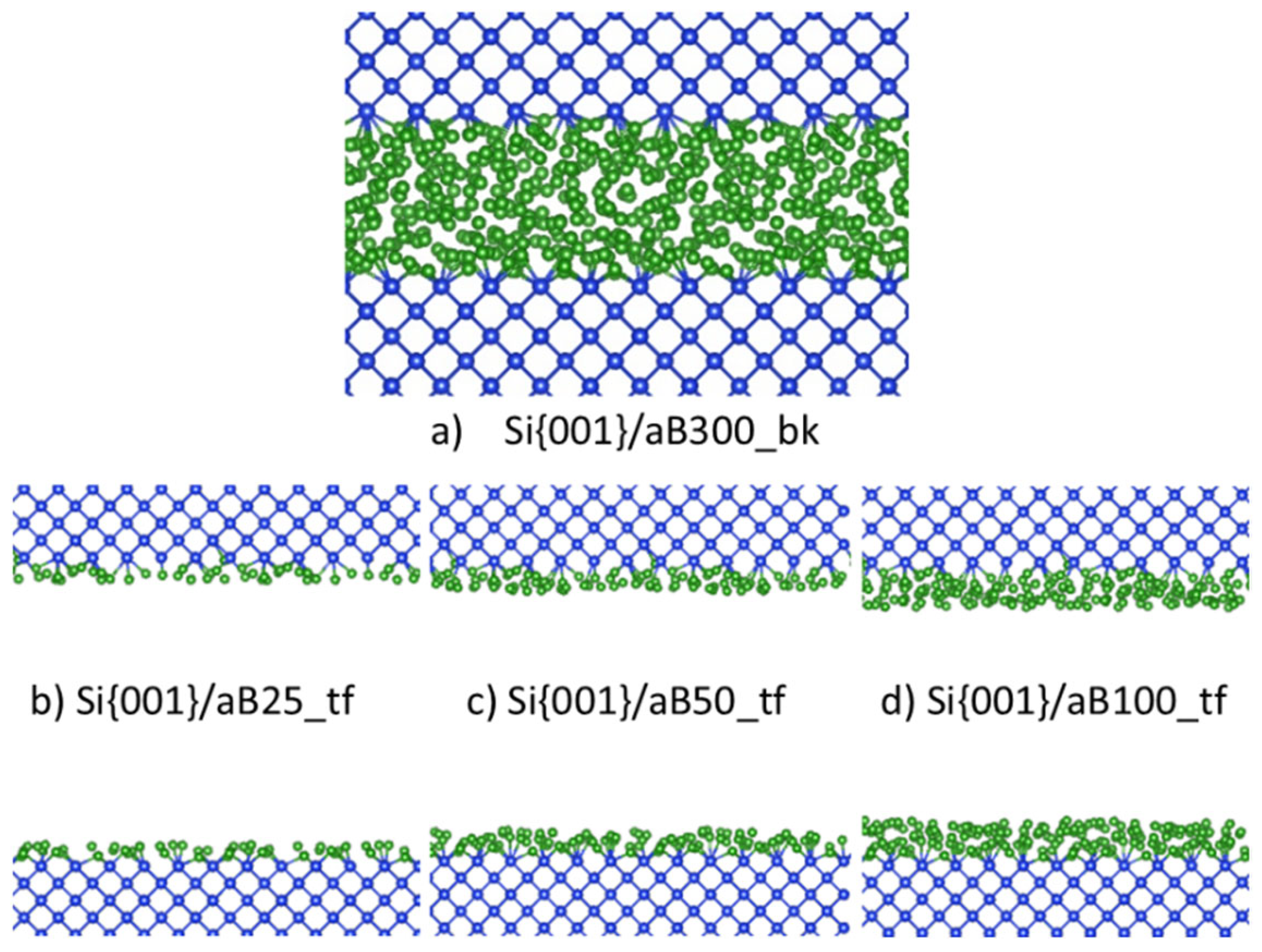
Figure 2.
A cross-sectional representation of the (a) input and (c) equilibrated system. (b) The dependence of the total valence-electrons energy of the system on the ab initio molecular dynamics simulation time. The free energy of the simulation nears the convergence value around approximately 0.5 ps.
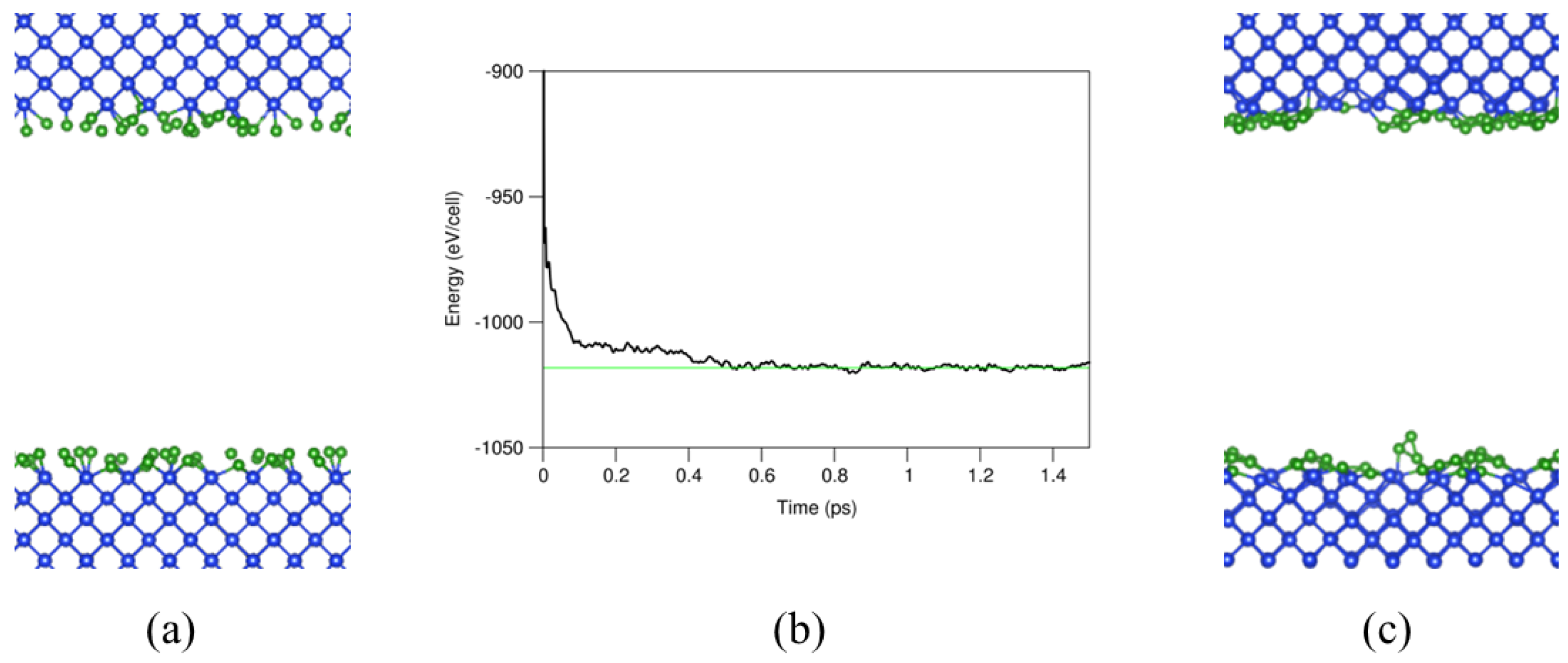
Figure 3.
The pDOS of the two species in α- B12. The Fermi level is indicated at 0 eV. The red and blue lines represent the s- and p-state contribution to the DOS. The black lines show the total DOS of the system.
Figure 3.
The pDOS of the two species in α- B12. The Fermi level is indicated at 0 eV. The red and blue lines represent the s- and p-state contribution to the DOS. The black lines show the total DOS of the system.
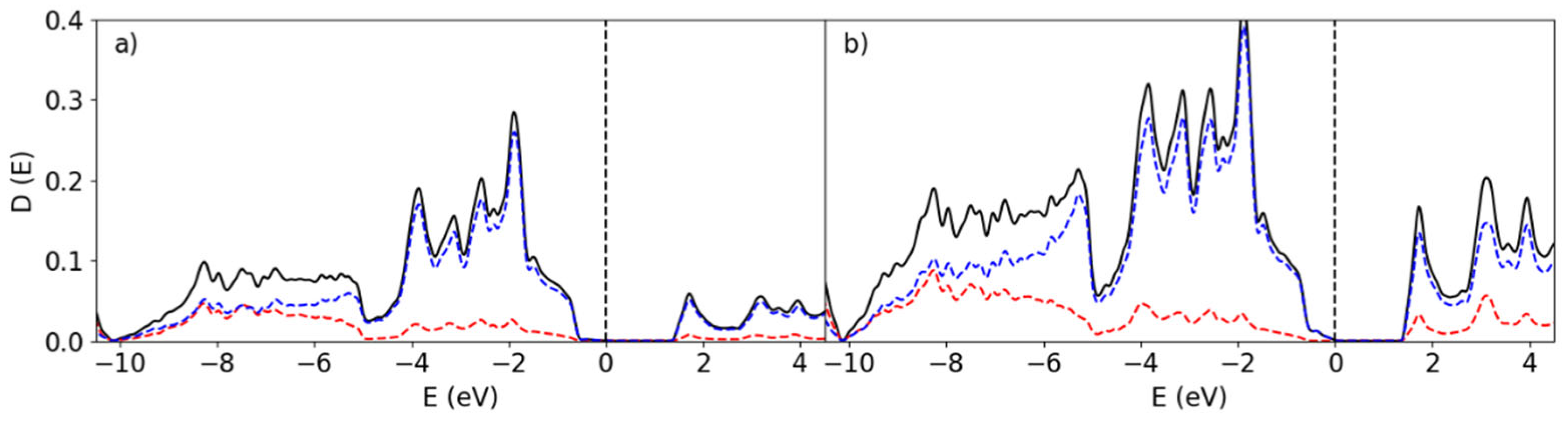
Figure 4.
The total DOS of the amorphous bulk B300 system.
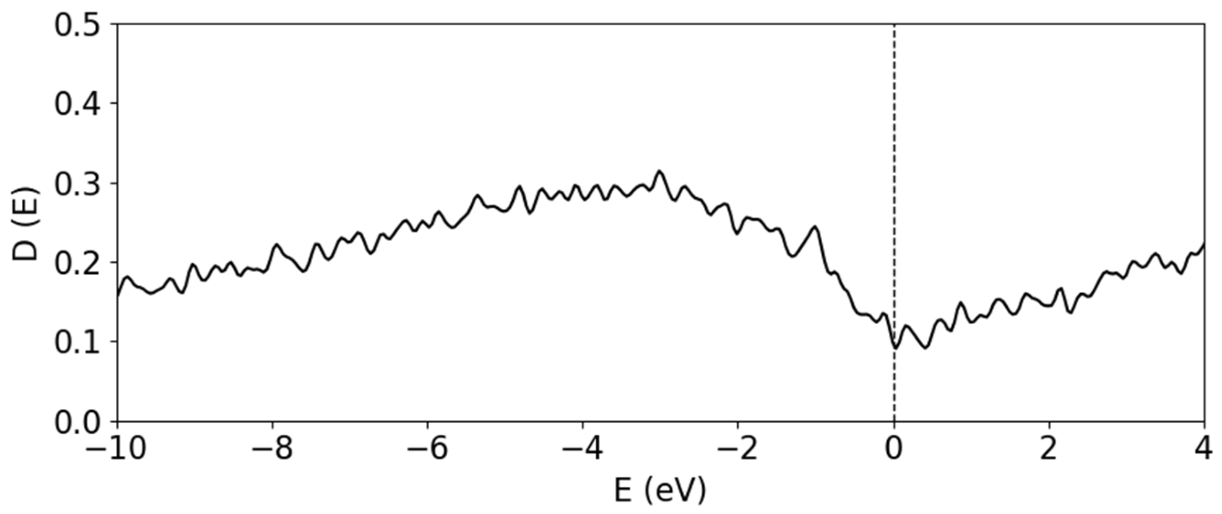
Figure 5.
A cross-sectional view from the (100)-plane of the (a) B25/Si, (b) B50/Si and (c) B100/Si. (d-f) The cross-section from the (110)-direction showing the top 3 layers of c-Si and the Si-B interaction at the interface after relaxation calculations of the atomic positions after removing the excess atoms. Furthermore, a typical representation of Si atom coordination with (g) one B atom, (h) two B atoms and (i) three B atoms. The blue and green spheres represent Si and B, respectively. The Si-Si, B-B and Si-B bonds with a length of less than 2.6, 1.8 and 2.2 Å respectively are drawn.
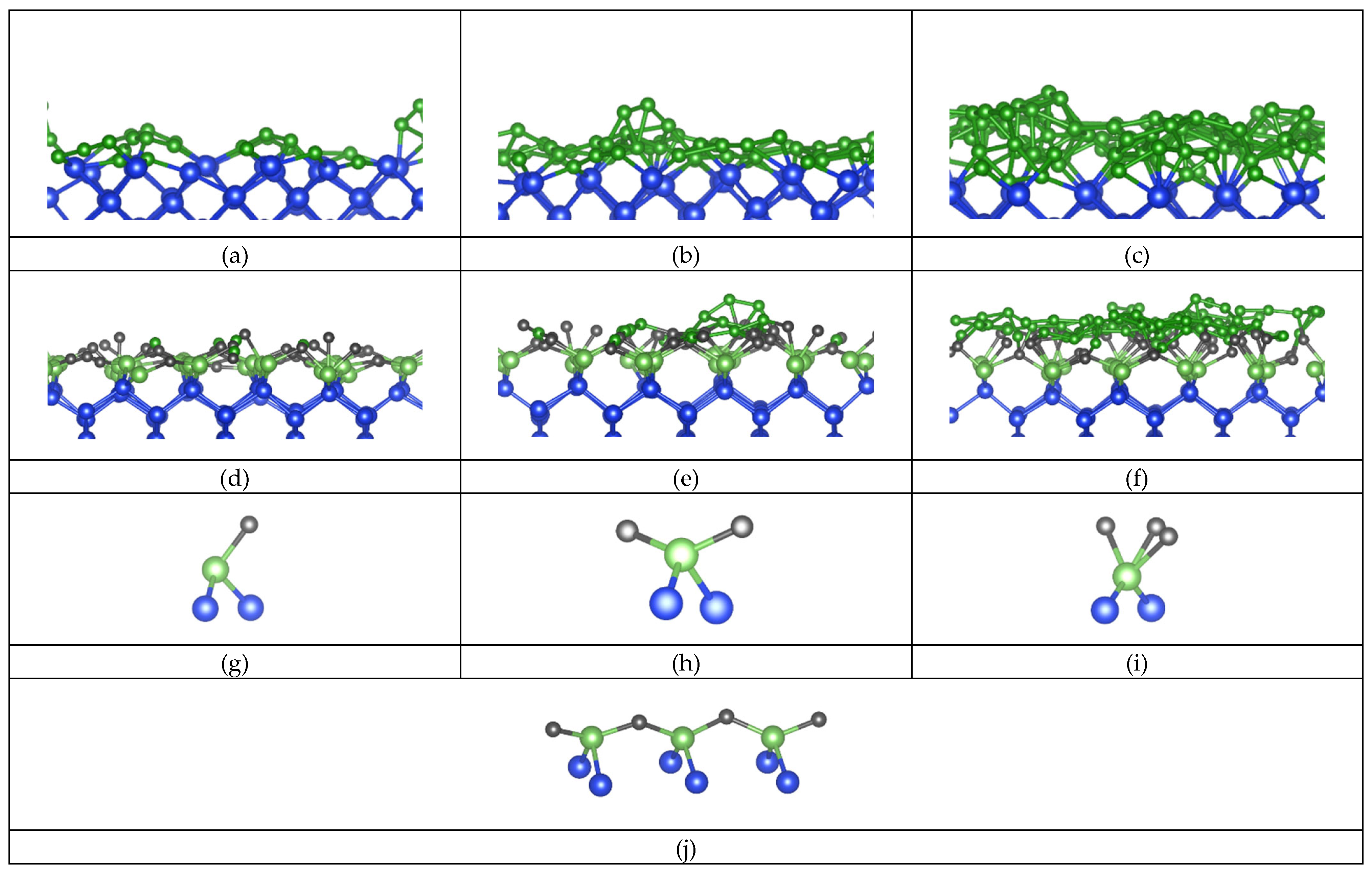
Figure 6.
Distribution of the number of B atoms coordinating with a Si atom for the (a) B25, (b) B50 and (c) B100 on Si144 interfaces.
Figure 6.
Distribution of the number of B atoms coordinating with a Si atom for the (a) B25, (b) B50 and (c) B100 on Si144 interfaces.
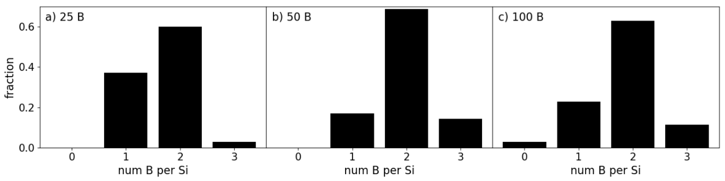
Figure 7.
Partial DOS at the B25/Si144 interface for the (a) Si and (b) B atoms, the surface Si atoms coordinated with (c) 1 B (d) 2 B (e) 3 B atoms, the interface B atoms interacting with (f) 1 Si and (g) 2 Si atoms and (h) B atoms without any Si-B interaction. The red and blue lines correspond to the s and p states, respectively.
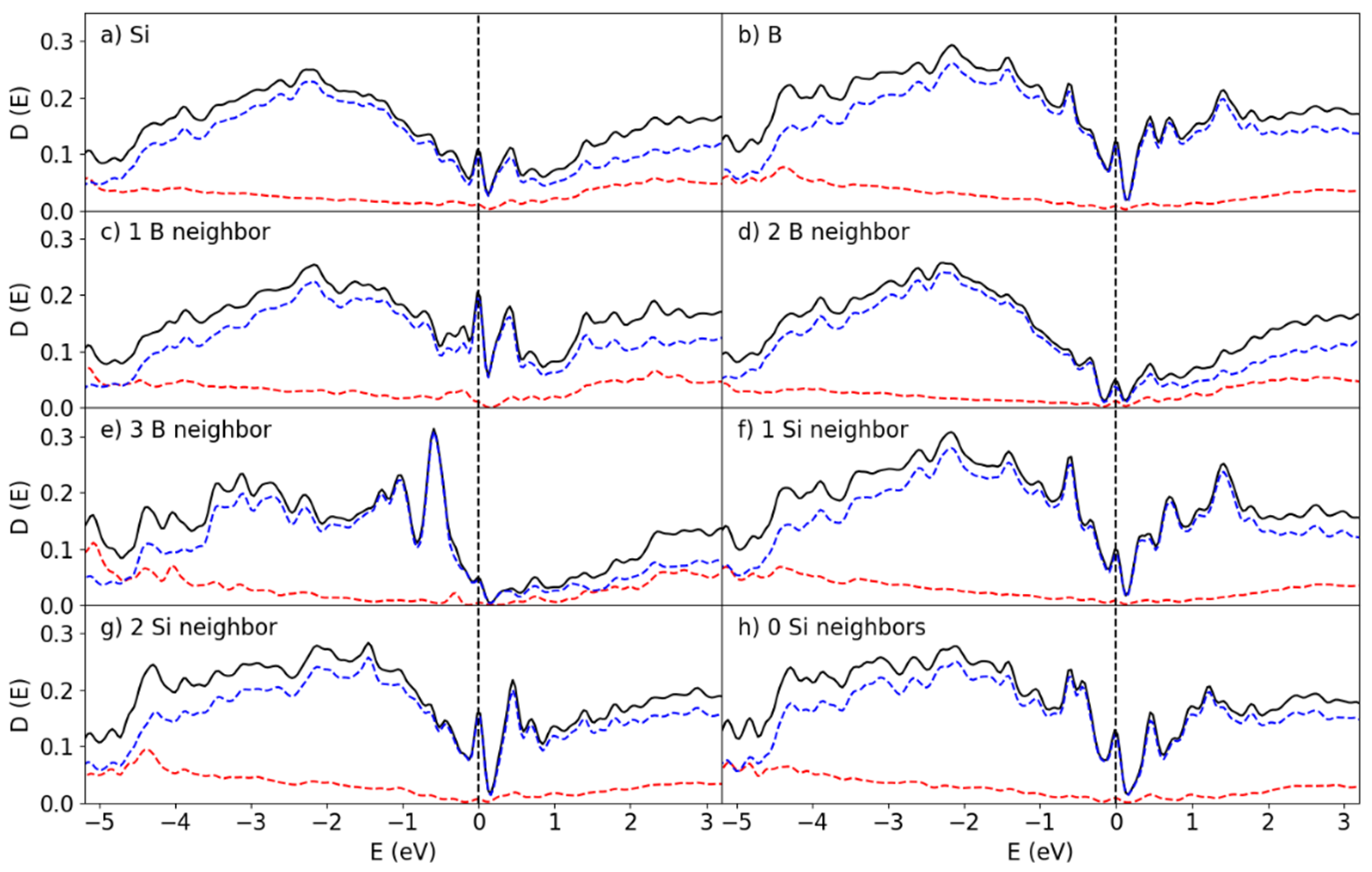
Figure 8.
Partial DOS at the B50/Si144 interface for the (a) Si and (b) B atoms, the surface Si atoms coordinated with (c) 1 B (d) 2 B (e) 3 B atoms and the interface B atoms interacting with (f) 1 , (g) 2 and (h) no Si atoms. The red and blue lines correspond to the s and p states, respectively.
Figure 8.
Partial DOS at the B50/Si144 interface for the (a) Si and (b) B atoms, the surface Si atoms coordinated with (c) 1 B (d) 2 B (e) 3 B atoms and the interface B atoms interacting with (f) 1 , (g) 2 and (h) no Si atoms. The red and blue lines correspond to the s and p states, respectively.
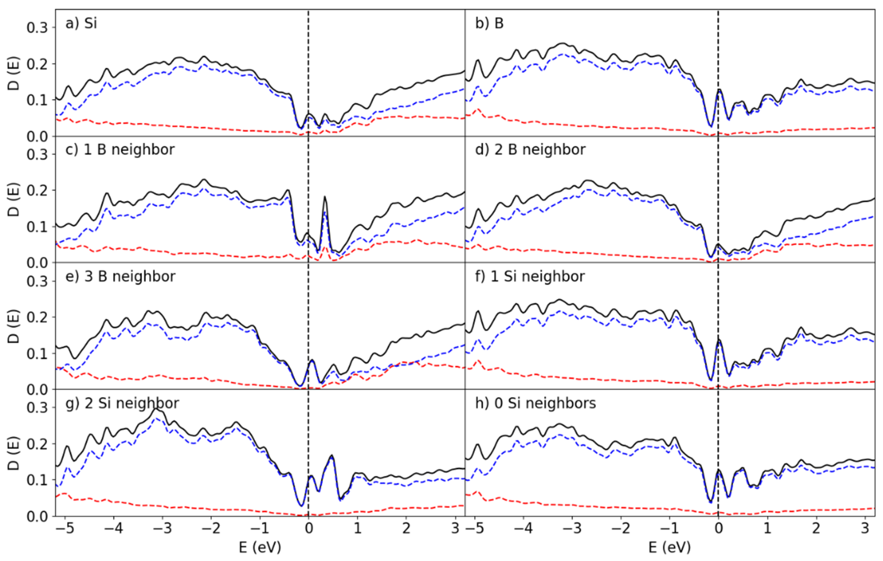
Figure 9.
Partial DOS at the B100/Si144 interface for the (a) Si and (b) B atoms, the surface Si atoms coordinated with (c) 1 B (d) 2 B (e) 3 B atoms and the interface B atoms interacting with (f) 1 Si and (g) 2 Si atoms, in addition to (h) the pDOS for the B atoms away from the interface. The red and blue lines correspond to the s and p states, respectively.
Disclaimer/Publisher’s Note: The statements, opinions and data contained in all publications are solely those of the individual author(s) and contributor(s) and not of MDPI and/or the editor(s). MDPI and/or the editor(s) disclaim responsibility for any injury to people or property resulting from any ideas, methods, instructions or products referred to in the content. |
© 2026 by the authors. Licensee MDPI, Basel, Switzerland. This article is an open access article distributed under the terms and conditions of the Creative Commons Attribution (CC BY) license (http://creativecommons.org/licenses/by/4.0/).
Copyright: This open access article is published under a Creative Commons CC BY 4.0 license, which permit the free download, distribution, and reuse, provided that the author and preprint are cited in any reuse.


