
Submitted:
03 April 2025
Posted:
04 April 2025
You are already at the latest version
Abstract
Two-dimensional (2D) n-MoS2 nanosheet (NSs) synthesized by sol-gel method was deposited on p-type heavily boron-doped diamond (BDD) film to form n-MoS2/p-degenerated BDD (DBDD) heterojunction device. The PL emission of the heterojunction exhibits a good prospect in the application of yellow light-emitting optoelectronic devices. From room temperature (RT) to 180℃, the heterojunction all exhibits typical rectification characteristics with good thermal stability, the rectification ratio and forward current decrease, the reverse current increase. Compared with the n-MoS2/p-lightly B-doped (non-degenerate) diamond heterojunction, the heterojunction demonstrates a significant improvement in both rectification ratio and ideal factor. At 100°C, the rectification ratio reaches the maximum value and is considered an ideal high temperature for achieving optimal heterojunction performance. When the temperature exceeds 140 ℃, the heterojunction transforms into the Zener diode. The heterojunction electrical temperature dependence is due to the Fermi level shifting resulting in the weakening of the carrier interband tunneling injection. The n-MoS2 NSs/p-DBDD heterojunction will broaden the subsequent research application prospects in the field of high-temperature consumption of future optoelectronic devices.
Keywords:
n-MoS2 NSs/p-DBDD heterojunction
; photoluminescence
; high temperature
; electrical transport behavior
1. Introduction
The transition metal disulfide structure MoS2 is one of the typical channel materials for semiconductor pn junction due to its atomically thin n-type properties [1], the single layer to multi-layer corresponds to the number of layers and the external electric field can be adjusted from the direct band gap semiconductor (1.9 eV) to the natural indirect band gap (1.2 eV), leading to the tunable and large-scale applications of electronic and optoelectronic properties [2]. With the increasing demand for nano-materials in optoelectronic devices, nanosized MoS2 seems to have solved various problems in developing excellent optoelectronic devices [3] such as transistors [5], sensors [6], LEDs [7], photodetectors [8,9] and so on because of its good mechanical properties, high carrier mobility, high absorption coefficient and strong electron hole constraints. MoS2 has become a hot material to replace the past materials and enter the new development stage of the nano-era [10]. However, the heterostructure formed by different morphologies of MoS2 nanostrctures (such as 2D thin films and nanosheets), which were combined with various substrates incuding MoSe2 [11], WSe2 [12,13], GaN [14], GaAsSb [15], BA2PbBr4 [16] and MoGe2N4 [17] in the past decades, are mostly confined to room temperature in practical applications. Working in the harsh environments of the heterojunction (high temperature, strong radiation, high pressure) still faces challenges such as device failure and unsatisfactory performance [18]. Boron-doped diamond (BDD) is usually designed and applied in new high-quality high-temperature resistant optoelectronic devices due to its wide band gap, strong chemical stability and high thermal conductivity of p-type semiconductor [19]. At present, typical n-type nanostructured semiconductors (such as ZnO [20], Ga2O3 [21], and WO3 [22]) have formed p-n heterojunction devices with p-type diamond to construct high-quality new diode terminal extension devices. Recently, we have investigated the optoelectrical carrier transport behavior of n-MoS2/p-light B-doped (non-degenerate) diamond heterojunction, which has typical rectification characteristics when working in high-temperature environment [23]. Nevertheless, p-diamond possess degenerative characteristics and probably generate band to band tunneling through heavily doping boron elements, which significantly affects the electrical properties of heterojunctions when combined with other n-type semiconductors [24]. Considering the possibility of carrier transport behavior change caused by heterojunction composed of n-MoS2 and p-DBDD. In this study, the 2D n-MoS2 NSs/p-DBDD films heterojunction was designed and the optoelectrical carrier transport performance was in depth researched innovatively. From room temperature (25 ℃, RT) to 180 ℃, the heterojunction all demonstrates representative rectification properties with excellent thermal stability, the rectification ratio and forward current decrease, and the reverse current increases. The rectification ratio reaches the maximum at 100 °C. Compared with the n-MoS2/p-lightly B-doped (non-degenerate) diamond heterojunction in our previous work, the heterojunction demonstrates a significant improvement in both rectification ratio and ideal factor. The fabricated n-MoS2 NSs/p-DBDD heterojunction demonstrates superior current density and evolves into Zener diode with increasing temperature, while the n-MoS2 NSs/p-lightly BDD heterojunction transitions into the reverse diode with increasing temperature.The optoelectrical transport behavior depending on temperature was analyzed by combining energy band diagram and semiconductor theoretical model, which provides a new direction for the high-quality research and development of n-MoS2 NSs related heterojunction optoelectronic devices in the harsh environment.
2. Materials and Methods
In an instrument filled with flowing gases H2 and CH4, heavily boron doped p-type diamond films were prepared on a silicon wafer substrate by hot-filament chemical vapor deposition (HFCVD) method. The boron source is provided by liquid trimethyl borate ((CH3O)3B), which is introduced into the chamber through H2 and the DBDD membrane is obtained by controlling the flow rate of H2. Subsequently, the DBDD membrane was washed with ethanol and deionized water in sequence to remove residual impurities on the surface. The DBDD has not been treated with irradiated, acid boiled and high temperature treatment, so it is hydrogen surface terminal.
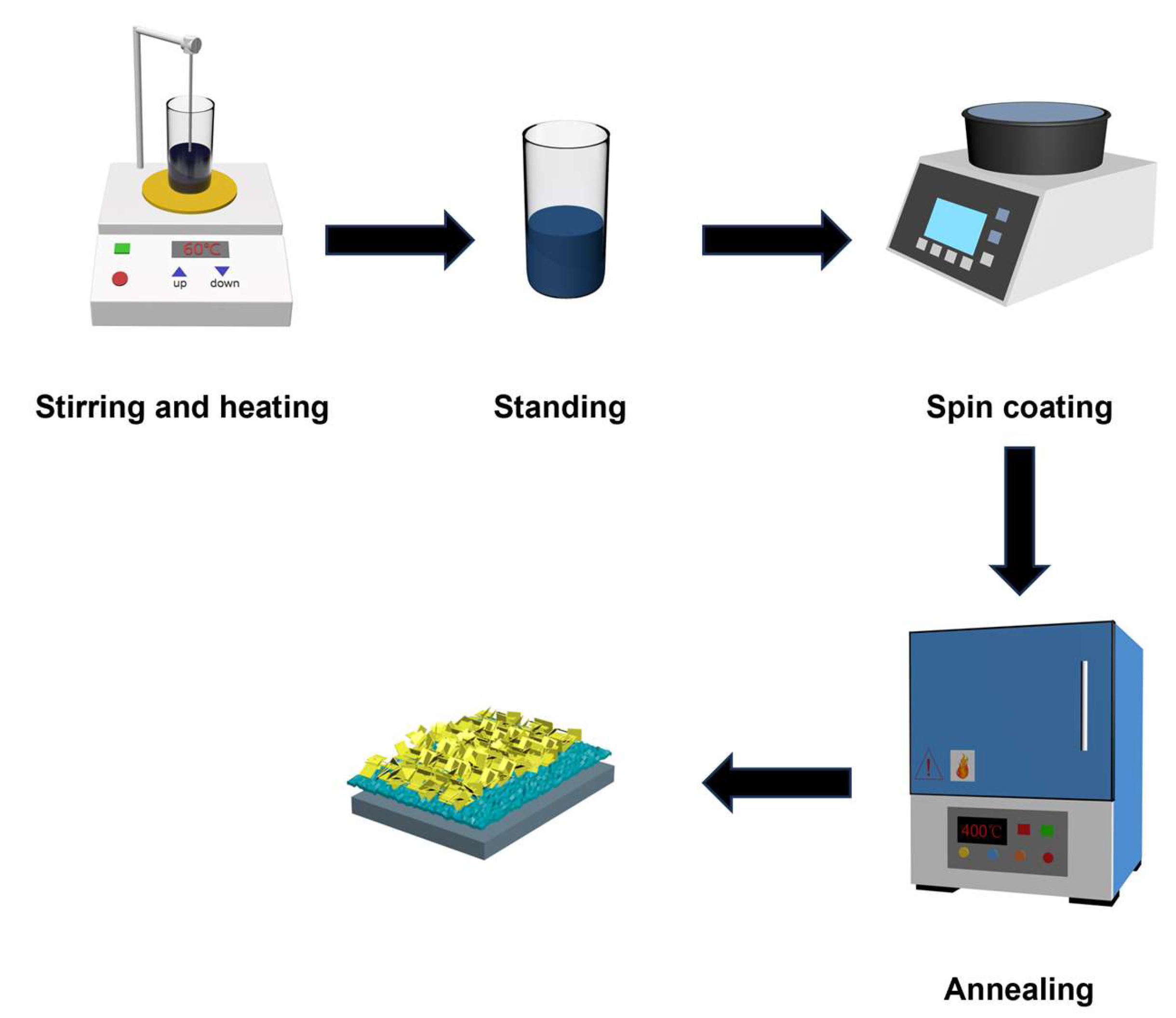
MoS2 nanosheets were prepared on DBDD film by sol-gel method. As shown in Scheme 1, [(NH4)6Mo7O24 · 4H2O] was used as the Mo source, CH3CSNH2 as the S source, and C14H23N3O10 as the chelating agent. The mixture was stirred continuously for one hour using a magnetic stirrer and dissolved in 8mL of deionized water to obtain a sol. Place the DBDD film based on silicon at the center of the spin coating machine, use a pipette to drop the sol onto the center of the DBDD film, and accelerate from 0 to 3000 rpm within 56 seconds. Take off the film and put it on a heating table at 60 ℃ to cure the coating on the DBDD film for 5 minutes, and then make the second deposition through the identical procedure to thicken the nanosheet with the annealing process at 400 ℃ and 4 hours to improve the quality of the bonded device. Scheme 2(a) illustrates the schematic structure of the n-MoS2 NSs/p-DBDD heterojunction. The MoS2 NSs are brought into contact with the conductive side of transparent indium tin oxide (ITO) glass and secured by using cyanoacrylate adhesive to prevent direct contact between the conductive copper wires and TiO2, and the BDD at the bottom of the contact could readily cause a short circuit, which can be effectively prevented by employing ITO as a dielectric. The ITO and conductive copper wires are connected with silver paste, respectively, to fabricate the heterojunction anode and cathode. The linear I-V characteristics between the ITO/Ag and BDD/Ag contacts demonstrate a linear relationship of an ohmic contact (Scheme 2(b)).
Scanning electron microscope with energy dispersive X-ray spectroscopy (SEM, Thermo Fisher Scientific FIB-SEM GX4, USA) was used to examine the element distribution and structural morphology of the samples. Set the scanning speed of the X-ray diffractometer (XRD, D8 ADVANCE, Germany) at 5°/min to check the phase structure and purity of the sample. The molecular structures of MoS2 NSs and p-degenerated BDD were detected with the excitation wavelength of 532 nm by a Raman spectrometer (Raman, inVia, UK), and the heterojunction electrical properties were tested with the Keithley 2400 source (Keithley Instrument, Cleveland, Ohio, USA). The carrier concentration of the DBDD film was utilized by the Hall effect (ET9110-HS, China).
3. Results and Discussion
Figure 1(a-c) displays the morphological characteristics of the 2D n-MoS2 NSs with the size range of 1 to 3 μm. Compared to p-light B-doped diamond film without twinning and with smoother crystallographic facets in our previous work, the p-degenerated B-doped diamond films exhibit obvious twinned crystal characteristics. The twinned crystal and abundant grain boundaries of p-degenerated BDD films are beneficial to the nucleation of MoS2 NSs. The MoS2 NSs is densely and randomly distributed on p-DBDD film with a lateral size of about 1.1 μm and a thickness of 98.4 nm. The thickness of 96 nm obtained by local scanning of atomic force microscope (AFM) confirmed the accuracy of results of SEM shown in Figure 1(d-e). The 2D MoS2 NSs fixed on p-DBDD film show uniform coverage, and has a large leakage boundary and specific surface area indicating outstanding photoelectric detection advantages [25]. The elements mapping measurement of the MoS2 NSs was further confirmed according to the EDS mapping spectral area as shown in Figure 1(f). The observation shows that the elements detected on the heterojunction are C, Mo and S as shown in Figure 1(g-i), which proves the elements C, Mo and S coexist and have high purity. The above characterization proved the successful synthesis of the 2D MoS2 NSs on p-DBDD substrates, and no other peaks related to impurities were detected [26].
Figure 2(a) shows the XRD image of the n-MoS2 NSs/p-DBDD heterojunction. In addition to the diffraction peaks of (111) and (220) diamond films at 43.82° and 75.24°, three comparatively sharp diffraction peaks were observed at 14.37°, 61.58° and 68.99° respectively, which can be attributed to (002), (107), and (201) of 2H-MoS2 (JCPD 37-1492). The diffraction peaks at 33.51° and 55.97° are attributed to the presence of (101) and (106) crystal faces of the MoS2 structure [27]. The (220) peak of the diamond film is slightly larger than the (111) peak, indicating that the growth rate of the (220) crystal plane of diamond is greater than that of the (111) plane. Li et al.[28] mentioned in their study that the concentration of B element is closely related to the preferred orientation of diamond during CVD growth stage. The intensity ratio of (111) and (220) first decreases and then increases with the increase of B concentration, which is consistent with our experimental results. Figure 2(b) displays the typical Raman image of n-MoS2 NSs/p-DBDD heterojunction. The peak of diamond film at 1330 cm-1 comes from the central phonon band, and there is a wider Raman peak at 1520 cm-1, so there is graphite phase besides diamond phase [29]. In order to obtain accurate information about graphite phase, we fitted the data in the illustration with Lorentz. The Raman peak at 1330cm-1 is D-band. Generally, the D-band is more obvious in low doped diamond films [30]. The Raman peak at 1520cm-1 is G-band, which is attributed to the bond stretching of sp2 hybrid orbital of heavily boron-doped diamond [31]. The two peaks at 289 and 376 cm−1 match the E1g and E12g Raman vibration modes of the 2D n-MoS2 NSs [32]. These demonstrated the presence of 2H-MoS2 phase with semiconductor characteristics [33]. In addition, the J1 (154 cm-1) band specifies the in-plane shear pattern of one side of the alternating chain relative to the other side [34]. The vibration mode of J2 (241 cm-1) is connected with the displacement of the S atomic layer and Mo atoms, while the J3 mode obtained at 336 cm-1 contains stretching of one side of the serrated chain concerning the other side [35]. All vibration J modes are ascribed to the twisted 1T phase superlattice structure. Therefore, the n-MoS2 NSs can reveal both metalline and semiconductor features (2H-MoS2 phase) simultaneously.
Figure 2(c) shows the photoluminescence (PL) spectra excited at 532 nm of the n-MoS2 NSs/p-DBDD heterojunction. There exsits an obvious peak at 568 nm (2.18 eV) due to the transition of exciton A [36,37]. The characteristic broad peak at 660 nm (1.87 eV) is caused by the recombination of A exciton [38]. In order to further verify the emission color quality of the device, the PL emission CIE color coordinates as shown in Figure 2(e) are calculated, and the chromaticity coordinates appear around (0.492, 0.505), which indicates that the n-MoS2 NSs/p-DBDD heterojunction has a promising market in the research and development of yellow light emitting optoelectronic devices. In addition, the electroluminescence (EL) of the device observed in Figure 2(d) has rich spectral characteristics. In 2D MoS2, excitons dominate the absorption and emission characteristics and the recombination process directly related to bound excitons is determined from the angle of EL. MoS2 has application value as a tunable portable optical transmitter, in which EL is usually confined to the area adjacent to the electrical contact and depends on hot carrier process [39]. The EL spectrum of the device has three obvious luminescence peaks in the red region. EL emission peaks at 668 nm and 680 nm are allocated to exciton emission in MoS2 [40,41], while the emission peaks at 632 nm are allocated to exciton B emission. As shown in Figure 2(e), CIE color coordinates of EL emission data appear near red emission region (0.309, 0.694). Compared with n-MoS2 NSs/p-non-degenerated BDD heterojunction in our previous work, the intensity of photoluminescence and electroluminescence is increased by two times, and the PL emission changes from light blue to light yellow, and the EL emission changes from green to red [23].
In order to avoid short-circuiting of the electrodes, the conductive surface of ITO was used as a conductive cathode in contact with the surface of n-MoS2 NSs, and the p-DBDD film was used as a conductive anode with the cathode and anode separated by insulating adhesive. Silver paste and wires were pasted to the conductive side of the ITO conductive glass as the negative electrode. Fix the p-DBDD film as the positive electrode and the conductive side of the ITOs in contact with the MoS2 nanosheets to form a pathway. The size of the prepared heterojunction device is 0.25×0.25 cm as shown in Figure 3(a). The I-V characteristics of the Ag contacts to DBDD and ITO curve of shows linear properties indicating ohmic contact (Figure 3(b)). Hall test shows that the p-DBDD has a carrier concentration of 5.8×10²¹ and the resistivity of 1.05×10³ and a mobility of 6.8 cm2 V-1 s-1. Figure 3(a-f) suggests the electrical properties of the n-MoS2 NSs/p-DBDD heterojunction gauged from RT to 180 °C. The I-V curve display good rectification performance for all temperature. The turn on voltages is about 0.2 V at RT, 0.7 V at 100 ℃, 0.3 V at 120 ℃, 1 V at 140 ℃, 2.1 V at 160 ℃ and 0.7 V at 180 ℃, respectively. With the temperature increasing, the forward current decreases as the bias increase. At RT, the rectification ratio is about 34.46 and the forward current is 0.16 A at 6 V which is 34 times higher than the reported n-MoS2 NSs/p-non degenerated BDD heterojunction in our previous work [23]. When the temperature rises to 100 °C, the I-V characteristic shows fantastic rectification performance with the rectification ratio achieved to 8.11×10⁶ and decrease in the reverse saturation current of 5.18×10⁻⁹ A. Thus, 100 °C is supposed to the optimal with excellent performance temperature for forward rectifier diode n-MoS2 NSs/p-DBDD heterojunction. Zener diode were observed when the temperature was up to 140 °C–180 °C. When the breakdown voltage is lower than 4Eg/q, the reverse breakdown can be ascribed to Zener tunneling effect, where Eg and q are the semiconductor bandgap and electronic charge, respectively. This device has good application requirements in analog circuits and small signal detectors [42]. A noteworthy detail is that the reverse current of n-MoS2 NSs/p-DBDD heterojunction begins to be larger than that of 160 °C and 180 °C, in which the rectification ratio is 0.459 and 0.671 and the reverse conduction voltage is 2.1 and 0.7 V, respectively, as shown in Table 1. This is attributed to the increase in reverse carrier tunneling of heterojunctions at high temperatures. while the reported n-MoS2 NSs/p-non degenerated BDD heterojunction transform into a reverse diode with increasing temperature. In addition, the rectification ratio shows a trend of first increasing, then decreasing, and finally increasing. Due to the thermal excitation effect, the rectification ratio reaches its maximum value of 8.11 × 10⁶ at 100 ℃. At 160 ℃, due to the enhancement of reverse tunneling, the rectification ratio drops to the minimum value of 0.459. Compared with the n-MoS2 NSs/p-non degraded BDD heterojunction, the n-MoS2 NSs/p-DBDD heterojunction has better rectification ratio at room temperature and high temperature. At 100 ℃, the rectification ratio of n-MoS2 NSs/p-DBDD increased by 7.64 × 10⁶ times, which may be due to the addition of B atoms and high concentration of p-degenerate diamond carriers in heavily doped diamond, resulting in more carrier injection and tunneling [23].
In order to expand probing into the electrical transmission behavior in n-MoS2 NSs/p-DBDD heterojunction, Figure 3(h-i) is combined with the ideal diode Equations (1) and (2) [47,48]:
with
where Is is the reverse saturation current, q is the electronic charge, V is the applied voltage, n is the ideal coefficient, k is the Boltzmann constant, T is the absolute temperature, A is the contact area, and A* is the effective Richardson constant. At the basis of 0.1–0.5 V region, the ideality factor (n values) of the n-MoS2/p-DBDD is 8.98–9.33 from RT to 180 °C, which indicates that the positive values of n-MoS2 NSs/p-DBDD is stable. The n value was greater than 2 demonstrating that n-MoS2/p-DBDD heterojunction displays nonideal thermal emission properties that may be due to the existence of potential non-uniform barriers, deep-level assisted tunneling or parasitic rectification junctions at the n-MoS2 NSs/p-DBDD interface. It is noted that the result of n value was significantly lower than that of the reported n-MoS2/p-lightly boron doped BDD heterojunction (8.6-10.2) [49].
Based on the phenomenon of temperature induced changes in current and rectification ratio, the equilibrium energy band diagram of n-MoS2 NSs/p-DBDD was established using the Anderson model to explain the carrier migration behavior. Reasonable calculation shows the conduction band (CB) offset ΔEC (3.8 eV) is 10 times higher than the valence band (VB) offset ΔEV (0.37 eV) leading that the injection current is primarily involved in the injected holes in VB. Due to the small VB barrier height at RT, the carrier tunneling from the VB to the defect level band stemming from the MoS2 NSs surface state of was occupied and exhibited relatively higher current. Compared with p-non-degenerated BDD, the EF may approach the band edge and enter into the VB of diamond. The carriers could tunnel from the VB of diamond to the CB of MoS2 when forward bias is exerted, and show higher forward current and lower diode conduction voltage (Figure 4(a-b)). In contrast to p-non-degenerated BDD whose Fermi level resides within the forbidden band (exhibiting diffusion-dominated current), the Fermi level of the p-DBDD resides within the valence band (exhibiting tunneling-dominated current) at room temperature. Thus, this exhibit relatively higher current performance compared to p-non-degenerated BDD in our previous work. At the high temperature of 120 ℃, the barrier height of the VB offset increases, which makes it difficult for carriers to transition from VB to defect energy band, and the tunneling current gradually disappears. At this time, it is transformed into an ordinary p-n junction diode and shows low forward current and turn on voltage (Figure 4(c)). At 180 °C (Figure 4(d)), the p-DBDD and n-MoS2 thermally activated more charge carriers. In addition, due to the presence of a large number of free surface states and a larger surface area to volume ratio in MoS2 NSs, n-MoS2 NSs form near degenerate semiconductors that primarily determine electrical properties [45,46]. The EF may enter the valence band of n-MoS2 and the conduction band of p-DBDD near the edge of the band. When a bias is applied, as the tunneling current increases, carriers possibly tunnel from the valence band of n-MoS2 to the conduction band of p-DBDD with the type of Zener diode (Figure 3(f)).
The carrier migration behavior can also be explained the variation of work function as calibrated in Figure 4). The work function was computed using:
where Evac is the energy of the vacuum level [43]. Work-function values are the indicative of thermodynamic stability of electrons in the respective component of heterostructures, due to which on contact formation in the heterostructures, the migration of electrons would occur, due to electron chemical potential difference at the interface, until fermi-level equilibration. The difference of the work function of the heterojunction with the change of temperature leads to the rearrangement of the electron density at the heterojunction cross section, and generates an induced electric field, which promotes the separation and transfer of electrons and holes. With the increase of temperature, the work function of heterojunction p-diamond decreases, and the work function of n-MoS2 increases, so that the interface barrier of the heterojunction decreases and more carrier injection is generated at high temperature leading the increase of the tunneling current [44].
The curves at all temperatures in Figure 5(a-b) are divided into three regions to explore the current transfer mechanism. For low forward voltages (region I), the electrical properties at 25 °C, 100 °C, 120 °C, 140 °C, 160 °C, and 180 °C were directed correlation with temperature, and comply with the power law of I-V1.18, I-V1.22, I-V1.06, I-V1.45, I-V1.14, and I-V1.09, respectively. The I-V characteristics of n-MoS2 NSs/p-DBDD heterojunction followed the ohmic laws with linear relationship at low voltage and all temperatures [50]. In region II, it generally obeys to the I-exp(αV) relationship attributed to the existence of composite tunneling performance due to the wide bandgap semiconductors of MoS2 and diamond material. By fitting the curve of region II, the injection efficiency constant α values were calculated to be 0.63, 0.86, 0.56, 0.67, 1.32, and 0.74 of 25 °C, 100 °C, 120 °C, 140 °C, 160 °C and 180 °C, respectively [51]. At 160 °C, the exponents value was closest to standard vacuum diode value (1.5). At the higher voltage region III, the current transport properties comply with the laws of I-V1.81, I-V1.72, I-V1.14, I-V3.61, I-V2.21, and I-V1.75 of 25 °C, 100 °C, 120 °C, 140 °C, 160 °C, and 180 °C, respectively. Current has an exponential relationship with voltage, and the exponents are greater than 2 normally attributed to the conduction model of space charge limiting current (SCLC) transmission model, which indicates that SCLC mechanism is limited by a single dominant trap level [52]. The SCLC model with restricted traps can account for exponential values close to 2. At high temperatures, the number of excited holes increases, accumulating and expanding the space charge region within the junction, and according to the SCLC model, the current mechanism changes from J∝V2 to J∝V3/2, and thus the exponent is raised to a value greater than 2. At higher temperatures of 180°C, the exponent is falls down again, which exhibits an approximately close to linear ohmic-voltage-current relationship because fewer holes can be excited to injected from diamond VB to MoS2 VB with respect to the higher energy levels and mainly through tunneling effect [53].
The interface carrier transmission performance in n-MoS2 NSs/p-DBDD heterojunction can be investigated by fitting the plots of ln(I/V2) versus 1/V into three situations (Figure 5(c-d)). (I) For low bias voltage at high temperature, multiple carriers pass through the interface with the energy produced by thermal excitation to overcome the interface barrier. The carriers transport mechanism could be illustrated with Equation (3) to interpret thermionic emission:
where A is the area of the heterojunction, A* is the Richardson constant, d is the height of the potential barrier at the interface, фb is the height of the potential barrier at T = 0 K, ε0 is the dielectric constant of the vacuum, and εr is the dielectric constant of the semiconductor. Thus, the capability of thermionic emission to conquer the interface barrier height is dependent on the demand excitation temperature. As the temperature is insufficient to allow carriers to pass through the interface barrier, the carrier transfer is primarily concerned with the interface barrier tunneling mechanism that is identical to the energy band diagram illustration. (II) The interfacial carrier transfer mechanism for low bias voltage can be expounded by coupling the direct tunneling and energy band diagram (Eq. (4)):
where h is Planck’s constant, and m is the charge carrier effective mass. (III) For the higher voltage, the carrier transport mechanism primarily regards Fowler–Nordheim (F–N) tunneling and is commentated by Eq. (5):
Therefore, multiple carriers could acquire plenty of energy to pass through the thermionic emission barrier height at high temperature. Based on bias voltage, carrier injection could take place in direct tunneling to F–N tunneling at lower temperature. Besides, the emergence of inflection point (Vt) at RT–140 °C indirectly illustrated the presence of F–N and direct tunneling. As VtRT > 6.25 V, Vt100 > 2.3 V, Vt100 > 2.3 V, Vt140 > 4.6 V, Vt160 > 2 V and Vt180 > 1.40 V, 1/V exhibited a negative slope trend, implying the emergency of F–N tunneling effect the carrier electrical transport behavior varied, and 1/V took a logarithmic form, signifying the appearance of direct tunneling effect. In the F-N tunneling mechanism governing carrier transport, the n-MoS2 NSs/p-non-degenerated BDD heterojunction exhibits a higher turn-on voltage (VtRT =7.69V, Vt100 =6.67V, Vt120=3.84V, and Vt140=5.56V), whereas the n-MoS2 NSs/p-DBDD heterojunction demonstrates significantly reduced thresholds (VtRT=6.25V, Vt100=2.3V, Vt140=4.6V, Vt160=2V and Vt180=1.40V). Furthermore, compared with MoS2 NSs/p-non-degenerated BDD heterojunction, the n-MoS2 NSs/p-DBDD heterojunction needs smaller inflection point voltage and depends more on F-N tunneling conduction mechanism. The lower inflection point voltage at 160 ℃ and 180 ℃ determines that the heterojunction is more dependent on F-N tunneling mechanism, which opens a new perspective for erasing electrons in the field of memory devices. In addition, the phenomenon of large reverse current as applied the large voltage at high temperature can be attributed to thermionic activated carriers and amplified tunneling current [54,55].
4. Conclusion
In conclusion, the n-MoS2 NS/p-DBDD heterojunction have been prosperous fabricated with the obvious twin characteristics and abundant grain boundaries in p-DBDD films made the MoS2 NSs easier to nucleate. The I-V characteristics of the devices all show rectification characteristics at RT-180 °C, and the rectification ratio reaches the maximum at 100 °C, which is considered the optimal rectification temperature of heterojunction. In contrast to the n-MoS2 NS/p-ligntly BDD heterojunction which transitions into a reverse diode at elevated temperatures, the fabricated n-MoS2 NS/p-DBDD heterojunction exhibits Zener diode characteristics when operating above 140 °C. Zener diode was observed when the temperature was above 140 °C. The variation of the electrical transport behavior at different temperature are mainly attributed to the shift of Fermi level and the change of tunneling current. The rectification ratio and ideal factor of n-MoS2 NS/p-DBDD is significantly superior to the prepared n-MoS2 NS/p-non-degenerated BDD heterojunction. A noteworthy specific is that the n-MoS2 NS/p-DBDD heterojunction is more dependent on F-N tunneling and is suitable for operation under high temperature conditions. The n-MoS2/p-DBDD heterojunction supplies effective reference for the memory erasure technology application and the development of high-quality devices in extreme working environments.
Author Contributions
Writing – original draft, D.S., C.L.; Methodology, D.S., C.L., D.S., S.G., D.X. and Q.W.; Investigation, D.S., C.L., D.S., S.G., D.X. and Q.W.; Conceptualization, D.S., C.L., D.S., D.X. and Q.W.; Supervision, D.S., D.X. and Q.W.; Writing— review and editing, Q.W. All authors have read and agreed to the published version of the manuscript.
Funding
This research was funded by the National Natural Science Foundation of China (Grant Nos. 62104090 and 11604133), the Natural Science Foundation of Shandong Province (ZR2022QF135), the Science and Technology Plan of Youth Innovation Team for Universities of Shandong Province (Grant No. 2019KJJ019), the Introduction and Cultivation Plan of Youth Innovation Talents for Universities of Shandong Province and the Research Funding of Liaocheng University (Grant Nos. 318012016, 318051610, 318052136, and 318051612).
Conflicts of Interest
The authors declare that they have no known competing financial interests or personal relationships that could have appeared to influence the work reported in this paper.
References
- L.W. Liu, C.S. Liu, X.H. Huang, S.F. Zeng, Z.W. Tang, D.W. Zhang, P. Zhou, Tunable Current Regulative Diode Based on Van der Waals Stacked MoS2/WSe2 Heterojunction–Channel Field-Effect Transistor, Adv. Electron. Mater. 8 (2022) 2100869. [CrossRef]
- H.S. Nalwa, A review of molybdenum disulfide (MoS2) based photodetectors: from ultra-broadband, self-powered to flexible devices, RSC Adv. 10 (2020) 30529-30602. [CrossRef]
- L.R. Zou, D.D. Sang, Y. Yao, X.T. Wang, Y.Y. Zheng, N.Z. Wang, C. Wang, Q.L. Wang, Research progress of optoelectronic devices based on two-dimensional MoS2 materials. Rare Met. 42 (2023) 17-38. [CrossRef]
- L.R. Zou, X.D. Lyu, D.D. Sang, Y. Yao, S.H. Ge, X.T. Wang, C.D. Zhou, H.L. Fu, H.Z. Xi, J.C. Fan, C. Wang, Q. L. Wang, Two-dimensional MoS2/diamond based heterojunctions for excellent optoelectronic devices: current situation and new perspectives, Rare Met. 42 (2023) 3201-3211. [CrossRef]
- F. Wu, H. Tian, Y. Shen, Z. Hou, J. Ren, G. Gou, Y. Sun, Y. Yang, T.L. Ren, Vertical MoS2 transistors with sub-1-nm gate lengths, Nat. 603 (2022) 259-264. [CrossRef]
- J.M. Evans, K.S. Lee, E.X. Yan, A.C. Thompson, M.B. Morla, M.C. Meier, Z.P. Ifkovits, A.I. Carim, N.S. Lewis, Demonstration of a Sensitive and Stable Chemical Gas Sensor Based on Covalently Functionalized MoS2. ACS Mater. Lett. 4 (2022) 1475-1480. [CrossRef]
- C. Liu, Y. Lu, X. Yu, R. Shen, Z. Wu, Z. Yang, Y. Yan, L. Feng, S. Lin, Hot carriers assisted mixed-dimensional graphene/MoS2/p-GaN light emitting diode, Carbon, 197 (2022) 192-199. [CrossRef]
- X. Liu, S. Hu, Z. Lin, X. Li, L. Song, W. Yu, Q. Wang, W. He, High-performance MoS2 photodetectors prepared using a patterned gallium nitride substrate, ACS Appl. Mater. Interfaces, 13 (2021) 15820-15826. [CrossRef]
- S. Yang, Y. Liu, Y. Wu, F. Guo, M. Zhang, X. Zhu, R. Xua, L. Hao, High-performance flexible photodetectors based on CdTe/MoS2 heterojunction, Nanoscale, 16 (2024) 13932-13937. [CrossRef]
- O. Samy, S. Zeng, M.D. Birowosuto, A. El Moutaouakil, A review on MoS2 properties, synthesis, sensing applications and challenges, Crystals, 11 (2021) 355. [CrossRef]
- Y. Jeong, H.J. Lee, J. Park, S. Lee, H.J. Jin, S. Park, H. Cho, S. Hong, T. Kim, K. Kim, S. Choi, S. Im, Engineering MoSe2/MoS2 heterojunction traps in 2D transistors for multilevel memory, multiscale display, and synaptic functions, npj 2D Mater. Appl. 6 (2022) 23. [CrossRef]
- M.H. Jeong, H.S. Ra, S.H. Lee, D.H. Kwak, J. Ahn, W.S. Yun, J. Lee, W.S. Chae, D.K. Hwang, J.S. Lee, Multilayer WSe2/MoS2 Heterojunction Phototransistors through Periodically Arrayed Nanopore Structures for Bandgap Engineering, Adv. Mater. 34 (2022) 2108412. [CrossRef]
- X. Xiang, Z. Qiu, Y. Zhang, X. Chen, Z. Wu, H. Zheng, Y. Zhang, Gain-type photodetector with GFET-coupled MoS2/WSe2 heterojunction, Journal of Alloys and Compounds, 1002 (2024) 175475. [CrossRef]
- P. Jian, X. Cai, Y. Zhao, D. Li, Z. Zhang, W. Liu, D. Xu, W. Liang, X. Zhou, J. Dai, F. Wu, C. Chen, Large-scale synthesis and exciton dynamics of monolayer MoS2 ondifferently doped GaN substrates, Nanophotonics,12 (2023) 4475–4484. [CrossRef]
- W. Wang, W. Wang, Y. Meng, Q. Quan, Z. Lai, D. Li, P. Xie, S. Yip, X. Kang, X. Bu, D. Chen, C. Liu, J.C. Ho, Mixed-Dimensional Anti-ambipolar Phototransistors Based on 1D GaAsSb/2D MoS2 Heterojunctions, ACS Nano, 16 (2022) 11036-11048. [CrossRef]
- S. Parveen, P. K. Pal, S. Mukhopadhyay, S. Majumder, S. Bisoi, A. Rahman and A. Barman, Hot carrier dynamics in the BA2PbBr4/MoS2 heterostructure, Nanoscale, 17 (2025) 2800. [CrossRef]
- S. T. Nguyena, K. D. Pham, Theoretical prediction of the electronic structure, optical properties and contact characteristics of a type-I MoS2/MoGe2N4 heterostructure towards optoelectronic devices, Dalton Transactions, 53 (2024) 9072–9080. [CrossRef]
- Y. Yao, D. Sang, S. Duan, Q. Wang, C. Liu, Review on the Properties of Boron-Doped Diamond and One-Dimensional-Metal-Oxide Based PN Heterojunction, Molecules, 26 (2020) 71. [CrossRef]
- L. Wang, S. Cheng, C. Wu, K. Pei, Y. Song, H. Li, Q. Wang, D. Sang, Fabrication and high temperature electronic behaviors of n-WO3 nanorods/p-diamond heterojunction, Appl. Phys. Lett. 110 (2017) 052106. [CrossRef]
- Q. Wang, Y. Yao, X. Sang, L. Zou, S. Ge, X. Wang, D. Zhang, Q. Wang, H. Zhou, J. Fan, D. Sang, Photoluminescence and Electrical Properties of n-Ce-Doped ZnO Nanoleaf/p-Diamond Heterojunction, Nanomaterials, 12 (2022) 3773. [CrossRef]
- W. Lin, T.T. Wang, Q.L. Wang, X.Y. Lv, G.Z. Li, L.A. Li, G.T. Zou, Design of vertical diamond Schottky barrier diode with junction terminal extension structure by using the n-Ga2O3/p-diamond heterojunction, Chin. Phys. B, 31 (2022) 108105. [CrossRef]
- Y. Yao, D. Sang, S. Duan, Q. Wang, C. Liu, Excellent optoelectronic applications and electrical transport behavior of the n-WO3 nanostructures/p-diamond heterojunction: a new perspective, Nanotechnology, 32 (2021) 332501. [CrossRef]
- L. Zou, D. Sang, S. Ge, Y. Yao, G. Wang, X. Wang, J. Fan, Q. Wang, High-temperature optoelectronic transport behavior of n-MoS2 nanosheets/p-diamond heterojunction, J. Alloys Compd. 972 (2024) 172819. [CrossRef]
- D. Sang, J. Liu, X. Wang, D. Zhang, F. Ke, H. Hu, W. Wang, B. Zhang, H. Li, B. Liu, Q. Wang, Negative differential resistance of n-ZnO nanorods/p-degenerated diamond heterojunction at high temperatures, Fron. Chem. 8 (2020) 531. [CrossRef]
- K. Zhang, S. Feng, S. Kang, Y. Wu, M. Zhang, Q. Wang, Z. Tao, Y. Fan, W. Lu, Hybrid structure of PbS QDs and vertically-few-layer MoS2 nanosheets array for broadband photodetector, Nanotechnology 32 (2021) 145602. [CrossRef]
- Y. Zhang, W. Zeng, Y. Li, The hydrothermal synthesis of 3D hierarchical porous MoS2 microspheres assembled by nanosheets with excellent gas sensing properties, J. Alloys Compd. 749 (2018) 355-362. [CrossRef]
- H.Y. He, Z. He, Q. Shen, Efficient hydrogen evolution catalytic activity of graphene/metallic MoS2 nanosheet heterostructures synthesized by a one-step hydrothermal process, Int. J. Hydrogen Energy 43 (2018) 21835-21843. [CrossRef]
- H. Li, T. Zhang, L. Li, X. Lu, B. Li, Z. Jin, J. Zou, Investigation on crystalline structure, boron distribution, and residual stresses in freestanding boron-doped CVD diamond films, J. Cryst. Growth 312 (2010) 1986-1991. [CrossRef]
- D.S. Knight, W.B. White. Characterization of diamond films by Raman spectroscopy, J. Mater. Res. 4 (1989) 385-393. [CrossRef]
- D. Kumar, M. Chandran, M.S.R. Rao. Effect of boron doping on first-order Raman scattering in superconducting boron doped diamond films, Appl. Phys. Lett. 110 (2017) 191602. [CrossRef]
- A.C. Ferrari, J. Robertson, Interpretation of Raman spectra of disordered and amorphous carbon, Phys. Rev. B 61 (2000) 14095. [CrossRef]
- J. Huang, Z. Dong, Y. Li, J. Li, W. Tang, H. Yang, J. Wang, Y. Bao, J. Jun, R. Li, MoS2 nanosheet functionalized with Cu nanoparticles and its application for glucose detection, Mater. Res. Bull. 48 (2013) 4544-4547. [CrossRef]
- S. Erkan, A. Altuntepe, R. Zan, Synthesis of MoS2 thin films using the two-step approach, Niğde Ömer Halisdemir Üniversitesi Mühendislik Bilimleri Dergisi, 12 (2023) 297-301. [CrossRef]
- Z. Liu, L. Zhao, Y. Liu, Z. Gao, S. Yuan, X. Li, N. Li, S. Miao, Vertical nanosheet array of 1T phase MoS2 for efficient and stable hydrogen evolution, Appl. Catal., B 246 (2019) 296-302. [CrossRef]
- M. Naz, T. Hallam, N.C. Berner, N. McEvoy, R. Gatensby, J.B. McManus, Z. Akhter, G.S. Duesberg, A new 2H-2H′/1T cophase in polycrystalline MoS2 and MoSe2 thin films, ACS Appl. Mater. Interfaces, 8 (2016) 31442-31448. [CrossRef]
- W. Yin, X. Bai, X. Zhang, J. Zhang, X. Gao, W.W. Yu, Multicolor Light-Emitting Diodes with MoS2 Quantum Dots, Part. Part. Syst. Charact. 36 (2019) 1800362. [CrossRef]
- M. Baby, K. R. Kumar, Enhanced luminescence of silver nanoparticles decorated on hydrothermally synthesized exfoliated MoS2 nanosheets, Emergent Mater. 3 (2020) 203-211. [CrossRef]
- E. Ponomarev, I. Gutiérrez-Lezama, N. Ubrig, A.F. Morpurgo, Ambipolar light-emitting transistors on chemical vapor deposited monolayer MoS2, Nano Lett. 15 (2015) 8289-8294. [CrossRef]
- Y. Ye, Z. Ye, M. Gharghi, H. Zhu, M. Zhao, Y. Wang, X. Yin, X. Zhang, Exciton-dominant electroluminescence from a diode of monolayer MoS2, Appl. Phys. Lett. 104 (2014) 193508. [CrossRef]
- D. Li, R. Cheng, H. Zhou, C. Wang, A. Yin, Y. Chen, N.O. Weiss, Y. Huang, X. Duan, Electric-field-induced strong enhancement of electroluminescence in multilayer molybdenum disulfide, Nat. Commun. 6 (2015) 7509. [CrossRef]
- R. S. Sundaram, M. Engel, A. Lombardo, R. Krupke, A.C. Ferrari, P. Avouris, M. Steiner, Electroluminescence in single layer MoS2, Nano Lett. 13 (2013) 1416-1421. [CrossRef]
- X. Liu, D. Qu, H.M. Li, I. Moon, F. Ahmed, C. Kim, M. Lee, Y. Choi, J.H. Cho, J.C. Hone, W.J. Yoo, Modulation of quantum tunneling via a vertical two-dimensional black phosphorus and molybdenum disulfide p–n junction, ACS Nano, 11 (2017) 9143-9150. [CrossRef]
- J. F. Curry, T. Ohta, F. W. DelRio, P. Mantos, M. R. Jones, T. F. Babuska, N. S. Bobbitt, N. Argibay, B. A. Krick, M. T. Dugger, M, Chandross, Structurally Driven Environmental Degradation of Friction in MoS2 Films, Tribology Letters, 69 (2021) 96. [CrossRef]
- S. Singha, R. Puniaa, K. K. Panta, P. Biswasb, Effect of work-function and morphology of heterostructure components on CO2 reduction photo-catalytic activity of MoS2-Cu2O heterostructure, Chemical Engineering Journal, 433 (2022) 132709. [CrossRef]
- R. Kumar, W. Zheng, X. Liu, J. Zhang, M. Kumar, MoS2-Based Nanomaterials for Room-Temperature Gas Sensors, Adv. Mater. Technol. 5 (2020) 191062. [CrossRef]
- P. Rong, Y. Jiang, Q. Wang, M. Gu, X. Jiang, Q. Yu, Photocatalytic degradation of methylene blue (MB) with Cu1–ZnO single atom catalysts on graphene-coated flexible substrates, J. Mater. Chem. A 10 (2022) 6231-6241.
- A. Di Bartolomeo, F. Giubileo, G. Luongo, L. Iemmo, N. Martucciello, G. Niu, M. Fraschke, O. Skibitzki, T. Schroeder, G. Lupina, Tunable Schottky barrier and high responsivity in graphene/Si-nanotip optoelectronic device, 2D Mater. 4 (2016) 015024. [CrossRef]
- S. Mukherjee, S. Biswas, S. Das, S.K. Ray, Solution-processed, hybrid 2D/3D MoS2/Si heterostructures with superior junction characteristics, Nanotechnology, 28 (2017) 135203. [CrossRef]
- J.K. Kim, K. Cho, T.Y. Kim, J. Pak, J. Jang, Y. Song, Y. Kim, B.Y. Choi, S. Chung, W.K. Hong, T. Lee, Trap-mediated electronic transport properties of gate-tunable pentacene/MoS2 pn heterojunction diodes, Sci. Rep. 6 (2016) 1-8. [CrossRef]
- Y. Zhang, Y. Zhuang, L. Liu, P. Qiu, L. Su, X. Teng, G. Fu, W. Yu, The microstructure evolution during MoS2 films growth and its influence on the MoS2 optical-electrical properties in MoS2/p-Si heterojunction solar cells, Superlattices Microstruct. 137 (2020) 106352. [CrossRef]
- M. Dutta, D. Basak, p-ZnO∕n-Si heterojunction: Sol-gel fabrication, photoresponse properties, and transport mechanism, Appl. Phys. Lett. 92 (2008) 212112. [CrossRef]
- Z. Çaldıran, Modification of Schottky barrier height using an inorganic compound interface layer for various contact metals in the metal/p-Si device structure, J. Alloys Compd. 865 (2021) 158856. [CrossRef]
- Y. Yu, C. Wang, C. Jiang, I. Abrahams, Z. Du, Q. Zhang, J. Sun, X. Huang, Resistive switching behavior in memristors with TiO2 nanorod arrays of different dimensions, 485 (2019) 222-229. [CrossRef]
- R. Padma, G. Lee, J.S. Kang, S.C. Jun, Structural, chemical, and electrical parameters of Au/MoS2/n-GaAs metal/2D/3D hybrid heterojunction, J. Colloid Interface Sci. 550 (2019) 48-56. [CrossRef]
- B.K. Sarker, S.I. Khondaker, Thermionic emission and tunneling at carbon nanotube–organic semiconductor interface, ACS Nano, 6 (2012) 4993-4999. [CrossRef]
Scheme 1.
Diagram of synthesis of n-MoS2 NSs/p-DBDD heterojunction by sol-gel method.
Scheme 2.
(a) the schematic structure of the n-MoS2 NSs/p-DBDD heterojunction. (b) the ohmic contact tests of Ag/ITO/Ag and Ag/DBDD/Ag.
Scheme 2.
(a) the schematic structure of the n-MoS2 NSs/p-DBDD heterojunction. (b) the ohmic contact tests of Ag/ITO/Ag and Ag/DBDD/Ag.
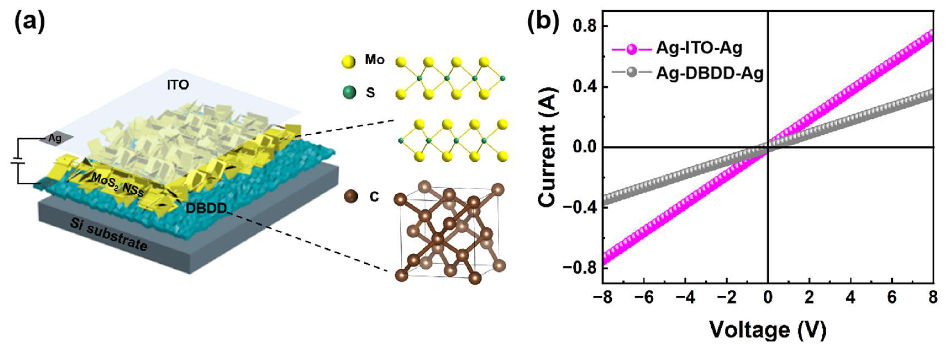
Figure 1.
SEM of the (a) p-DBDD film. (b-c) the MoS2 NSs (d) AFM image of MoS2 NSs on p-DBDD film. (e) the cross-section of AFM. (f) EDS spectra of n-MoS2 NSs/p-DBDD heterojunction. (g-i) EDS mapping images of C, Mo, S.
Figure 1.
SEM of the (a) p-DBDD film. (b-c) the MoS2 NSs (d) AFM image of MoS2 NSs on p-DBDD film. (e) the cross-section of AFM. (f) EDS spectra of n-MoS2 NSs/p-DBDD heterojunction. (g-i) EDS mapping images of C, Mo, S.
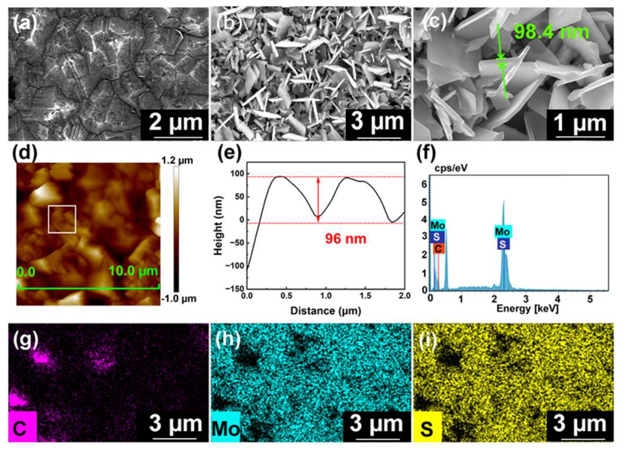
Figure 2.
(a) XRD pattern (b) Raman pattern of n-MoS2 NSs/p-DBDD heterojunction; Inset displays the Raman detection of p-DBDD. (c) PL spectra of n-MoS2 NSs/p-DBDD heterojunction. (d) EL spectra of n-MoS2 NSs/p-DBDD heterojunction. (e) CIE chromaticity diagram of PL and EL.
Figure 2.
(a) XRD pattern (b) Raman pattern of n-MoS2 NSs/p-DBDD heterojunction; Inset displays the Raman detection of p-DBDD. (c) PL spectra of n-MoS2 NSs/p-DBDD heterojunction. (d) EL spectra of n-MoS2 NSs/p-DBDD heterojunction. (e) CIE chromaticity diagram of PL and EL.
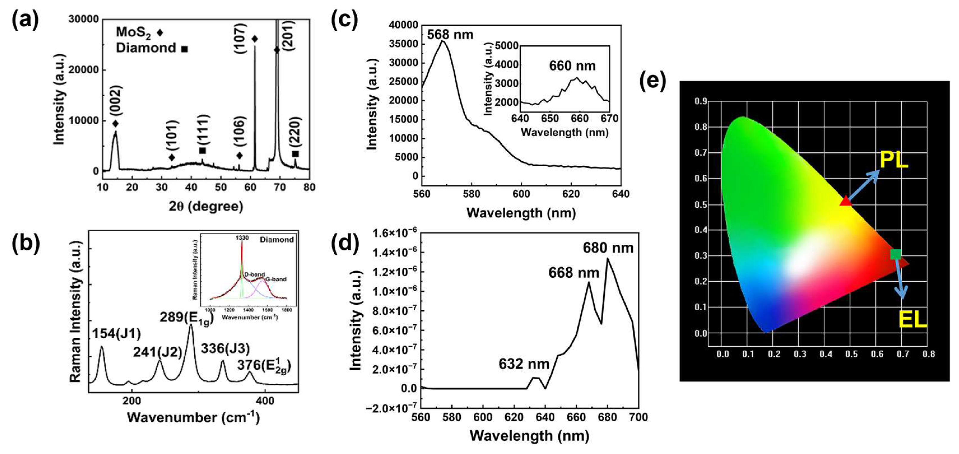
Figure 3.
(a-g) I-V plots of n-MoS2 NSs/p-DBDD heterojunction at RT, 100 ℃, 120 ℃, 140 ℃, 160 ℃, 180 ℃. The inset of (a) is the schematic diagram of n-MoS2 NSs/p-DBDD heterojunction device. The inset of (b) is the Ag/BDD/Ag and Ag/ITO/Ag ohmic contact. (h-i) lnI-V curves.
Figure 3.
(a-g) I-V plots of n-MoS2 NSs/p-DBDD heterojunction at RT, 100 ℃, 120 ℃, 140 ℃, 160 ℃, 180 ℃. The inset of (a) is the schematic diagram of n-MoS2 NSs/p-DBDD heterojunction device. The inset of (b) is the Ag/BDD/Ag and Ag/ITO/Ag ohmic contact. (h-i) lnI-V curves.
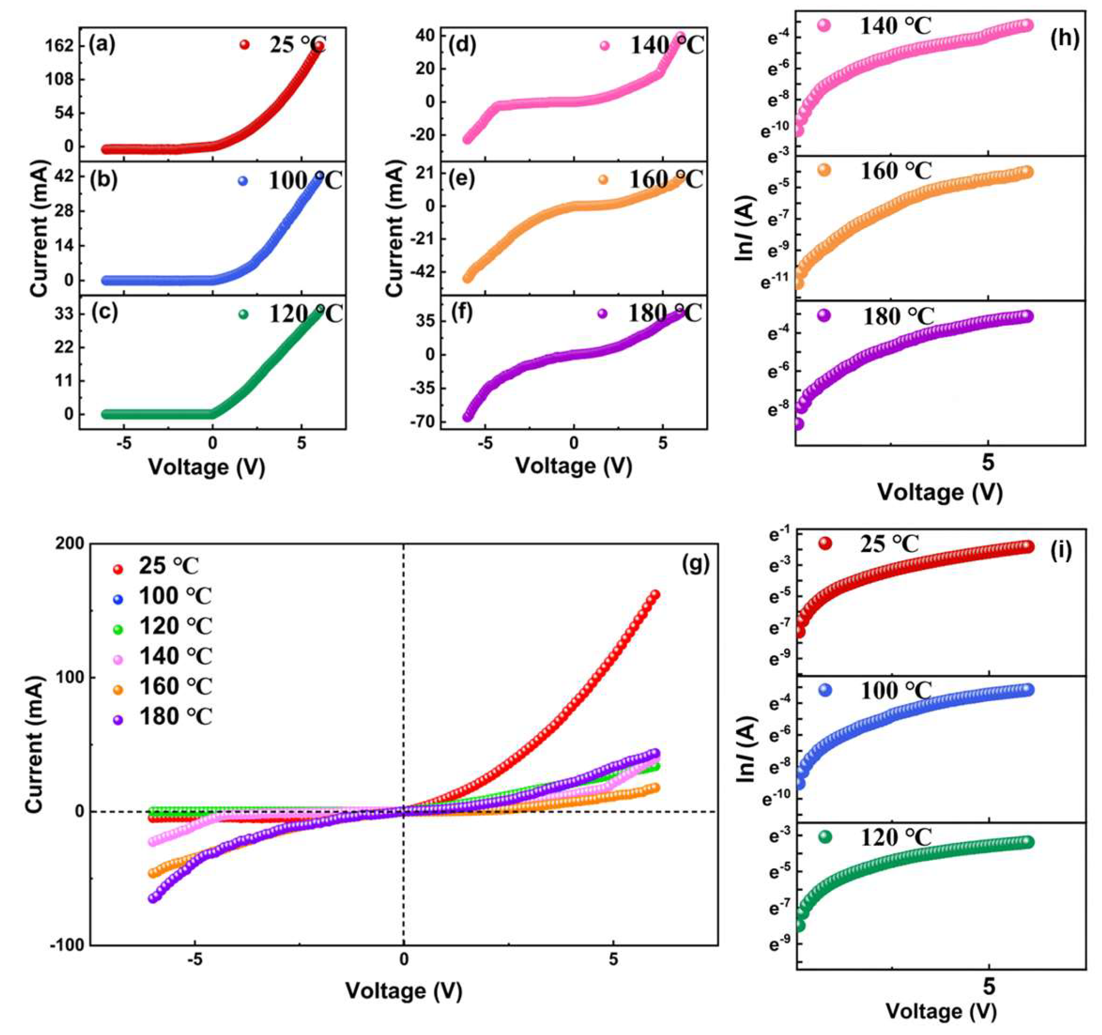
Figure 4.
Energy band diagrams of (a) n-MoS2 NSs/p-non-degenerated BDD heterojunction at RT; n-MoS2 NSs/p-DBDD heterojunction at (b) RT; (c) 120 ℃; (d) 180 ℃.
Figure 4.
Energy band diagrams of (a) n-MoS2 NSs/p-non-degenerated BDD heterojunction at RT; n-MoS2 NSs/p-DBDD heterojunction at (b) RT; (c) 120 ℃; (d) 180 ℃.
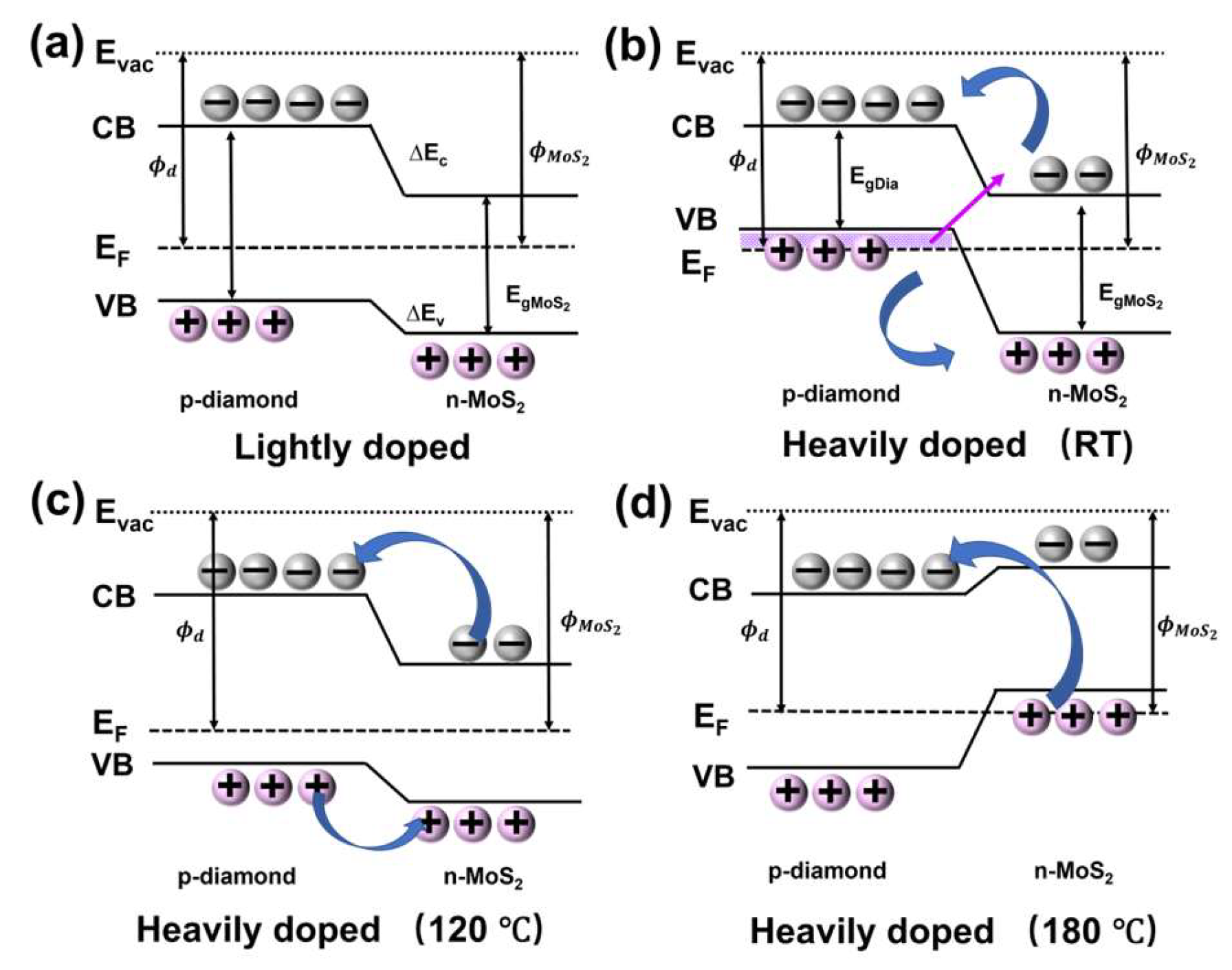
Figure 5.
(a-b) logI-logV plots; (c-d) ln(I/V2) versus 1/V plots of n-MoS2 NSs/p-DBDD heterojunction from RT to 180 ℃.
Figure 5.
(a-b) logI-logV plots; (c-d) ln(I/V2) versus 1/V plots of n-MoS2 NSs/p-DBDD heterojunction from RT to 180 ℃.
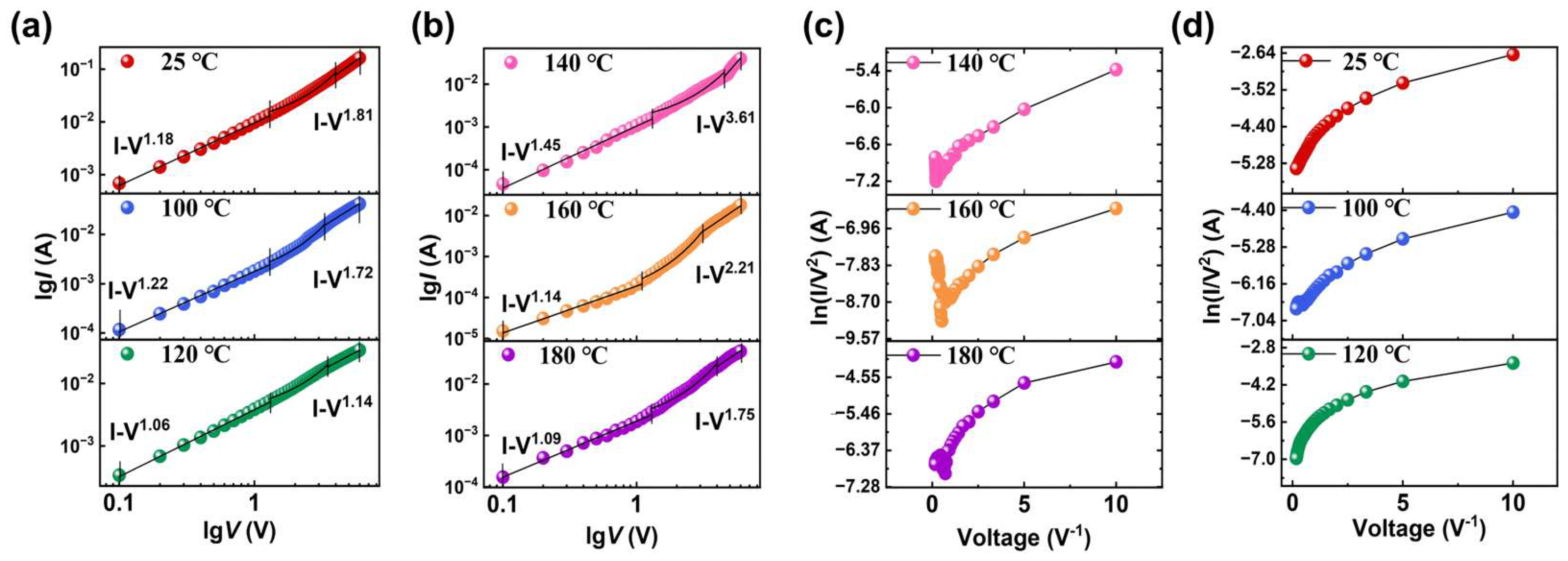

Table 1.
I-V behavior of device at variable temperature.
| Temperature (℃) | RT | 100 ℃ | 120 ℃ | 140 ℃ | 160 ℃ | 180 ℃ |
| Current at 6 V (A) | 0.167 | 0.042 | 0.033 | 0.039 | 0.017 | 0.043 |
| Current at -6 V (A) | 0.004 | 5.18×10⁻⁹ | 3.78×10⁻⁷ | 0.022 | 0.046 | 0.064 |
| Rectification ratio | 41.75 | 8.11×10⁶ | 8.73×10⁴ | 1.772 | 0.459 | 0.671 |
| Turn on voltage (V) | 0.2 | 0.7 | 0.3 | 1 | 2.1 | 0.7 |
| Ideality factor | 8.98 | 8.82 | 9.73 | 7.78 | 9.71 | 9.33 |
Disclaimer/Publisher’s Note: The statements, opinions and data contained in all publications are solely those of the individual author(s) and contributor(s) and not of MDPI and/or the editor(s). MDPI and/or the editor(s) disclaim responsibility for any injury to people or property resulting from any ideas, methods, instructions or products referred to in the content. |
© 2025 by the authors. Licensee MDPI, Basel, Switzerland. This article is an open access article distributed under the terms and conditions of the Creative Commons Attribution (CC BY) license (http://creativecommons.org/licenses/by/4.0/).
Copyright: This open access article is published under a Creative Commons CC BY 4.0 license, which permit the free download, distribution, and reuse, provided that the author and preprint are cited in any reuse.


