
Submitted:
23 January 2026
Posted:
26 January 2026
You are already at the latest version
Abstract
The paper introduces a novel control approach that integrates Proportional-Integral-Derivative (PID) control with a Linear Quadratic Regulator (LQR) for a Full-Bridge Boost Converter (FBBC). To enable effective linear control design, the FBBC system is linearized around its steady-state operating. The control architecture is structured into four cases: Case 1: PI-LQR Output Feedback, Case 2: PI-LQR State Feedback, Case 3: PID-LQR Output Feedback, and Case 4: PID-LQR State Feedback. Each case is evaluated for system responsiveness by examining output voltage stability, inductor current dynamics, and control signal characteristics. The analysis aims to identify the optimal and most reliable system performance under input voltage disturbance and load variation. The simulation results indicate that Case 3 (PID-LQR Output Feedback) consistently delivers the best performance, characterized by the shortest settling time, optimal control signal, and fast response to disturbances.
Keywords:
integrated PID-LQR
; full-bridge boost converter
; small signal modeling
; state feedback
; optimal control
1. Introduction
The function of power converter is to regulate and optimize the power flow between the energy source and the load, so that the efficiency, stability, and reliability of the system can be improved according to the characteristics and operational needs of its applications [1,2,3,4,5]. One of the most widely used power converter is DC–DC converter, considering the many electronic devices that require a specific operating voltage that is different from the voltage of the energy source [2,6]. The DC–DC converter is capable of performing voltage regulation functions, either by increasing the voltage (boost), decreasing the voltage (buck), or a combination of both (buck–boost), according to system requirements [7]. Especially in applications with limited energy sources such as batteries, which generally produce relatively low voltages, boost type converters become very important to increase the output voltage to match the load requirements [8,9]. This role makes the boost type DC–DC converter essential in a variety of modern electronic systems, including portable devices, renewable energy systems, and electric vehicles.
In general, the main components of a boost converter consist of an inductor, a switching device, a diode, and a capacitor [6]. The working principle of the boost converter depends on the state of the switch. When the switch is in the “ON” state, current flows to the inductor and energy is stored in the form of a magnetic field. At this time, the load does not receive direct supply, so the output voltage decreases. On the other hand, when the switch is in the “OFF” state, the stored energy in the inductor is released, and the current flows through the diode to the capacitor and the load. This causes the output voltage to increase as a result of the sum of the source voltage and the inductor voltage [10].
In the implementation which electrical isolation is important, e.g. battery charging and vehicle auxiliary power supply, isolated dc-dc converter is required. The isolated type of boost converter is named as full-bridge boost converter (FBBC). This topology uses four active switches arranged in a full-bridge configuration, combined with a high frequency transformer and diodes rectifier. Similar to conventional boost converter, the input is connected to an inductor and the output to a capacitor. The main advantages of this topology are higher power conversion efficiency, and the ability to transfer large power without significantly increasing the size or complexity of the circuit [11,12,13].
Even though using four switching devices, instead of one in conventional boost converter, the operation principle of FBBC is similar to conventional boost converter. The change of switch state does not cause sudden changes in the output voltage, resulting in a nonlinear relationship between the duty cycle to the output voltage [14]. Small changes in the duty cycle, especially when approaching unity, can cause significant output voltage fluctuations. This increases the risk of oscillation and instability [15]. In addition, the behavior of the voltage and current in the converter is not only influenced by the duty cycle but also by the input voltage and the load. This complexity is happened when the system operates in Continuous Conduction Mode (CCM) where the inductor current never drops to zero during one switching cycle [16]. This makes the analysis and design of control systems more challenging.
Selecting the right control method is an important part in designing a control system for a power converter, especially in FBBC. Along with the development of technology, various controller methods have been proposed and implemented to improve system performance, especially in terms of transient response, stability, and resilience to disturbances. For example, research in [17,18] proposed the proximal policy optimization (PPO) method, which is one of the algorithms in reinforcement learning that is able to adapt dynamically to variations in load and input voltage. This method shows the advantage of obtaining faster settling time and better system stability compared to conventional control methods. Furthermore, research in [19] developed a fast terminal sliding mode control (FTSMC) method that is capable of fast reference tracking and produces low overshoot. This method also shows good resilience to external disturbances and superior performance compared to conventional sliding mode control and proportional-integral (PI) control. In addition, artificial intelligence-based approaches have also been applied, such as the heuristic dynamic programming (HDP) method, which utilizes artificial neural networks as an approximation function. This method is able to effectively overcome large disturbances and shows better performance compared to conventional PI control, especially under startup conditions and load variation changes [20,21]. Moreover, a backstepping-based approach combined with current-mode control has also been studied in [22,23,24,25,26]. The results show that this method is able to maintain system stability and has better resilience to load variations compared to the conventional cascaded PI control method.
According to several previous studies, the design of control systems for FBBC remains an unresolved research challenge that requires additional attention in control system development. Conventional controllers, such as proportional-integral (PI) or proportional-integral-derivative (PID), frequently use static tuning approaches that are insufficiently responsive to system dynamics produced by changes in load and input voltage. This constraint impairs the capacity to maintain output voltage stability, especially under high transient situations. Furthermore, conventional controllers struggle with overshoot, settling time, and steady-state error, as well as frequently inefficient in producing smooth, non-fluctuating control signals. On the other hand, optimal control techniques such as the Linear Quadratic Regulator (LQR) have not been frequently or efficiently utilized in FBBC control designs, particularly when combined with the PID structure, which is well-established and reliable in many industrial applications. To improve the performance of FBBC-based power conversion systems, a unique methodology is required that combines the capabilities of both conventional and optimal control methods.
Based on the aforementioned issues, this paper proposes a novel control approach which integrates the PID and LQR methods to improve the dynamic performance of the FBBC system through a small-signal modeling framework. This approach is a novel contribution to the area, seeking to improve system robustness against disturbances and obtain superior performance metrics such as fast rise time, accurate transient response, low or zero overshoot, short settling time, and near-zero steady-state error. Furthermore, the proposed PID-LQR controller explicitly incorporates delay time considerations into the control system design to address issues such as overvoltage and undervoltage, maintain overall system stability, and accelerate disturbance rejection In addition, this study performs a thorough analysis of the output voltage (capacitor voltage), inductor current, and duty cycle responses under various control strategies to demonstrate the effectiveness and superiority of the proposed PID-LQR approach for modern power conversion systems, specifically FBBC.
The paper is arranged with the following structure: Section 2 provides a summary of the performance of the full-bridge boost converter system. Section 3 described a small-signal modeling approach. The PID-LQI is discussed in Section 4. Section 5 explains the result and discussion, whereas section 6 contains the study's conclusions.
2. Full-Bridge Boost Converter
The main components of FBBC include inductor, switches, transformer, diodes, capacitor, and load, as can be seen in Figure 1. The bridge uses four switches (MOSFET or IGBT) to convert the DC voltage to high-frequency AC voltage for the transformer. The transformer output voltage is then converted back to DC voltage through a rectifier and filter. The advantages of FBBC are increasing the output voltage, providing isolation between the input and output sides, handling large power, and producing high efficiency. Generally, FBBC is used in high-power applications such as solar power systems, large-capacity battery charging systems, and electric vehicles.
The operation process of this FBBC depends on the condition of the switches i.e. S1, S2, S3, and S4. If the switch is in the "ON" condition, the current flows to the inductor and stores energy in the form of a magnetic field. In this case the output voltage drops because it does not receive a direct supply. If the switch is in the “OFF” condition, the inductor releases its energy, so that the output voltage increases due to the combination of the source voltage and the induced voltage. During the operation, the crossed switches are activated simultaneously, for example S1 is activated simultaneously with S4 and S2 is activated simultaneously with S3. This activation has a phase shift of 180⁰ as presented in Figure 2, with Vab is line to line voltage, Vo is output voltage without filter, d is duty cycle, and Ts is the switching frequency.
Referred to Figure 1, the switching cycle of the FBBC has four periods. In periods 1 and 3, all switches are in the ON conditions. In this period the inductor is in a charged state. In period 2, the switches S1 and S4 in the ON condition and the other switches are in the OFF status, so that energy is released from the inductor. During period 4, the switches S2 and S3 are in the ON condition and the other switches are in the OFF status, so that the inductor releases energy. For more details, each period is presented in Figure 3.
From the equivalent circuit in Figure 3a, for the 1st and 3rd periods, it depicts all switches in ON status. Based on Kirchoff's law, the mathematical equations for input voltage and capacitor voltage are written in (1) and (2), respectively. Meanwhile, the output voltage can be written in equation (3).
with notations of , , , , , , and are the input voltage, the stray resistance inductor, the inductor current, the capacitor voltage, the load resistance, the stray resistance capacitor, and the output voltage, respectively. From (1)-(3), the state space and the output equation can be written as in (4) and (5).
For the period two as in Figure 3b, based on Kirchoff's law, the relationship between load current, inductor current, and capacitor current can be written as , where the load current is , the inductor current is , the transformer winding ratios is , and the capacitor current is . From this relationship, the output voltage equation is obtained as follows:
Meanwhile the input voltage can be written as , where the transformer primary voltage is . By substituting (6) to the input voltage equation, the differential equation of inductor current can be written as:
Then according to Kirchoff’s law, the relationship between inductor current, capacitor current, and load current can be written as where the output current is . From this, the differential equation of capacitor voltage can be written as:
From (6) to (8), by using similar state variables, the input variable, and the output variable, the state space and the output equation can be written as:
From Figure 3c, we find that the state space and output voltage equations are similar to period 2, i.e. (9) and (10).
3. Small Signal Modeling
The FBBC is a complex and nonlinear dynamic system, so that the application of conventional linear methods is inadequate to analyze the system dynamics and to design the control system. To overcome this, the small-signal modeling approach is one of the effective analysis methods to derive the system dynamics and to design the control of the converter. The purpose of small-signal modeling is to understand the dynamic response of the system due to small perturbations, represents a nonlinear system to become linear around certain operating point (steady-state), and enable a precise and efficient control system in the frequency and time domains [27]. The steps in small-signal modeling include:
3.1. Define the Steady State Operating Point
Steady-state operating point is the working condition of the converter when all variables (voltage, current, and duty cycle) are at fixed values and do not change with respect to time. This operating point is the basis for constructing the state-space averaged model and performing linearization. The steady-state operating point refers to fixed output voltage , fixed input voltage , fixed duty cycle , fixed inductor current , and fixed output current . Assuming that the FBBC operates in continuous conduction mode (CCM), then the relationship of steady state with output voltage, inductor current, and duty cycle is presented in (11), (12), and (13) respectively.
3.2. State Space Averaging Modeling
The state-space averaging model approach is a method commonly used to represent the dynamics of a switching converter system into a continuous-time linear model. The converter has two conditions, each with its state space equation. Defined the state variable consists of the inductor current [] and the capacitor voltage [], then can be written as . The equations are averaged model according to the PWM duty cycle as follows.
with , ,
and .
where , , , ,
, and . So, the state space in (14) and the output equation in (15) as the averaging of the two conditions ON and OFF is resulted as follows:
3.3. Introducing Small Perturbation
Small perturbation is an approach to introduce small perturbations to the main system variables such as inductor current, output voltage, and duty cycle to analyze the dynamics of the system due to changes in the linear system to the perturbation. Each variable is expressed as the sum of the average value and small perturbation, written with the following notation:
with is the state variable, is the operating point of the variable value from the steady state analysis, and is the deviation with respect to steady state value due to small perturbation. Based on (18), the small perturbation approximation for each state variable to the steady-state value can be written as follows:
with , , and are the steady state of the inductor current, output voltage, and duty cycle. , , and are the small perturbation of the inductor current, output voltage, and duty cycle respectively.
3.4. Linearization Model and Transfer Function
Linearization of the FBBC model is an important approach to simplify the nonlinear system into linear form in the time or frequency domain. The linearization for the state-space averaged model in (20) uses the Taylor approximation to obtain a low-order linear model. We substitute all variables into the averaged model and then linearize by ignoring the second-order components such as , and others. The linear small signal model in the time domain can be written as follows:
with is the state variable that describes the small perturbation of the system's steady-state condition for the inductor current () and the capacitor voltage () written as . is the small signal of input voltage in the form of input voltage deviation. is an external input in the form of a small perturbation of duty cycle. is the system output in the form of a capacitor voltage or converter output voltage. is the system matrix, is the input matrix, is the small perturbation matrix, is the system output matrix, and is the feedthrough matrix (the direct effect of small perturbation on the output). With , the system matrices can be written as follows:
, , ,
, and .
To simplify the control design process, we neglect the stray resistance in the above and we have
, , , , and .
And from (20) and (21) we have
4. PID-LQR Control Approach
Proportional-integral-derivative (PID) controller is the most commonly used feedback controller and is widely available due to its simplicity, reliability, ease of implementation, and flexibility in use. PID controllers have been around since the 1940s and are still relevant. It is proven by almost >95% of those engaged in the industrial sector using PID controllers. In general, PID works by calculating the error between the desired value (setpoint) and the actual value (system output), then correcting it automatically. PID has three components. The proportional component (P) functions to correct the current error by producing a control signal that is proportional to the magnitude of the error. The integral component (I) plays a role in correcting the accumulation of past errors by summing up errors over time, thereby reducing the steady-state error. While the derivative component (D) is used to estimate the direction and rate of future error changes by providing corrections based on the rate of error change over time. An interesting aspect of PID design is the difficulty in tuning the gain of Kp, Ki, and Kd. PID tuning is the process of determining the PID gain to achieve optimal system performance. If set incorrectly, this can cause the system to become unstable, unresponsive, or experience significant overshoot, oscillation, and steady-state errors. Other considerations in PID design include disturbances, changes in system conditions, and time delays, which can lead to ineffective PID controller designs. Solutions to overcome this problem usually involve a combination of PID with other methods.
This study proposes a novel control approach based on the integration of PID and Linear Quadratic Regulator (LQR) to enhance the dynamic performance of the FBBC system. The proposed method addresses the limitations of conventional controllers such as PI and PID, which often lack responsiveness to load and input voltage variations. In this approach, the PID gains are optimally tuned through the LQR framework, resulting in a more stable and precise control performance characterized by fast rise time, minimal overshoot, short settling time, and near-zero steady-state error. Key operational characteristics of the FBBC, such as duty cycle, input voltage, and load which contribute to the presence of delay time between the control signal and system response. If unaccounted for, this delay can degrade system efficiency and stability. Therefore, this research explicitly incorporates delay time into the control design, modeled using the Second Order Plus Time Delay (SOPTD) framework. By employing the PID-LQR approach, the control system is expected to achieve improved performance in terms of disturbance rejection, prevention of overvoltage and under voltage, and enhanced power conversion efficiency of the FBBC under various operating conditions. The PID-LQR controller is designed in two schematics: output feedback as seen in Figure 4a and state feedback (cascade) in Figure 4b.
Theorem 1: consideration a small-signal linear system that requires advantage of the time delay in control signal and the state variable with time delay is :
with the signal control where is , the state variable , the matrices are and . The approach that minimizes the quadratic performance index is expressed as follows:
with , and , are the state weighting matrix and the control weighting matrix respectively. The optimal control vector as:
with matrix is a unique solution of the Algebraic Riccati Equation (ARE) where (positive definite) as follows
For time delay, if , then . Because gives a control signal in time horizon , is not known directly at time t. Therefore, the optimal control vector (26) can be represented as
with .
Proof: if there is a time delay, the actual control signal at time is . Because is unknown at time t, it is necessary to anticipate the system’s condition at time horizon . Generally, the control law (26) is represented as . The linear system is represented as becoming , as in (24). Since , the closed-loop system for in the interval becomes . The state space can be expressed as the transient solution where . Incorporate the predicted state into the optimal control law. If , then is equivalent to (28). (proven)
Definition 1: for Output Feedback Controller (Figure 4a)
The state variable in (24) can be defined in general as . Using the second order plus time delay (SOPTD) transfer function, examine the following system: ) is the error system.
Definition 2: for Output Feedback Controller with integrator (Figure 4a)
To build a PID controller scheme with an output feedback structure, an augmented system can be created by adding a new state to the system in form of an integrator (24). The integrator variable equation is ,and the augmented state space can be expressed as:
with the state variable augmented , and matrices augmented are , . Using definitions 1 and 2, the generic canonical representation of the systems (24) and (30) can be stated as follows:
Theorem 2: the PID control signal is written in:
As stated by Theorem 1 in (26) and (28), the optimal control vector becomes
and the PID gains are obtained
Proof: Theorem 1 in (26) and (28) can be used to determine
with . The setting the characteristic equation of the closed loop systems can be written
To get the matrix , substitute (35) and (36) and obtain the characteristic equation of the closed loop system.
If P matrix is ARE solution in (27) and referred to (28) then
, and with
, , ,
, , ,
, and .
then the value of or . Thus, the optimal control vector corresponds to (32) and (33), resulting in PID gains according to (34). (proven).
Definition 3: for State Feedback Controller with integrator system (Figure 4b)
With the state variables as in Definition 1, referring to the second order plus time delay (SOPTD) transfer function in (22) and (23), considering the following system:
Inner-loop: ) and outer-loop: )
To construct a PID controller scheme with state feedback, according to definitions 3 and 2 in (38) it becomes:
Theorem 3: referred to definition 3, given the PID control signal is written in:
referring to Theorem 1 and 2, the optimal control vector for the inner-loop in (41) and outer-loop in (42) becomes
and the PID gains are obtained
inner loop
outer loop
Proof: according to Theorem 1 and 2, the matrix can be calculated by putting the characteristic equation of the closed-loop system . The P matrix represents the ARE solution. Thus, the optimal control vector is determined by (41) and (42), and the PID gains are derived using (43) and (44). (proven)
Remark: PI-LQR Controller
The second order plus time delay (SOPTD) transfer function can also be used to implement the PI controller’s output and state feedback.
Proof: without limiting generality, based on definitions 1 and 2 and without tracking error, the PI gain can be derived by tuning using LQR in accordance with Theorems 1 and 2. Thus, the optimal control vector can be expressed as:
For PI-LQR Output Feedback as (33)
For PI-LQR State Feedback as (41) and (42)
so that the PID gains are obtained:
For PI-LQR Output Feedback as (34)
For PI-LQR State Feedback as (43) and (44)
inner loop
outer loop
(proven).
5. Simulation Results and Discussion
The proposed control applications for FBBC are simulated using PSIM software. The FBBC parameter values can be seen in Table 1.
To obtain a deeper understanding of the system response characteristics, by entering the parameters in Table 1 into (20) and (21) the following numerical matrix is obtained:
, , , , and .
This dynamic system model provides a comprehensive understanding of the internal characteristics of the linearized FBBC around the operating point. The matrix indicates that the system has two states with significant cross-interactions and has relatively fast and oscillatory system dynamics. The eigenvalues of this matrix are and lie in the complex plane with negative real part, indicating that the system is stable but underdamped, thus having a tendency towards oscillatory response in the initial transient. With the matrix, the input directly affects the system only in the first state, while small perturbations of duty cycle interact with both states with the matrix indicating that the system has high sensitivity to disturbances especially in the first state. On the output side, the matrix indicates that the output signal is a linear combination of both states, with the dominant contribution coming from the second state. In addition, small perturbations of the duty cycle also directly affect the output with , which provides an important indication that disturbances will be manifested directly in the system response without any inherent damping. These characteristics indicate that the system requires a robust and adaptive controller design, given its sensitivity to input changes and load variations.
The performance of the FBBC open-loop system with duty cycle of 0.75 is examined in two conditions: (i) The input voltage is initially fixed at roughly 35 V from t = 0 to t = 4 seconds. At t ≈ 4 s, the input voltage is changed to 45 V and remains steady until t = 6 s, as shown in Figure 5a. (ii) The load changes from 200 Ohm to 100 Ohm at 2 second, as indicated by the load signal as shown in Figure 5b. With duty cycle od 0.75, the desired output voltage is 350 V.
Figure 5c illustrates the transient response of the inductor current in the FBBC system. This graphic shows three transient circumstances that occur at times around 0 s, 2 s, and 4 s. At 0 – 2 seconds, with input voltage of 35 V and load of 200 Ohm, the inductor current is in average of 16.67 A at steady state. When the load changes to 100 Ohm, the inductor average current becomes 31.81 A. With the load is kept being 100 Ohm and the change occurs in the input voltage to 45 V, the inductor average current becomes 40.89 A.
Meanwhile, Figure 5d illustrates the transient response of the capacitor voltage in the FBBC system. This graph illustrates that the output voltage is more sensitive to the changes in the input voltage than the load. However, the output voltage remains rather steady around the nominal value. In the time range of 0 to 2 seconds, the average output voltage is 333.24 V, 318.02 V at 2 to 4 seconds, and 408.89 V at 4 to 6 seconds. In general, we can find steady state error at all time ranges. This is frequent in open-loop systems since there is no error correction, necessitating the employment of a controller in closed-loop systems.
Adding a controller to the closed-loop FBBC system results in three eigenvalues: −1.1404, and −0.0023±0.0022i. The Lyapunov stability criterion indicates that the system is asymptotically stable, as all three eigenvalues have negative real portions. The eigenvalue -1.1404 is a fast dominant mode, indicating the system's ability to respond to shocks or reference changes with a relatively quickly damped transient component. These characteristics indicate the presence of an underdamped response, which reduces oscillations before the system reaches a steady state. This system exhibits steady behaviour, making it suited for FBBC control in the setting of eigenvalues with high stability (negative real part), fast reaction, and substantial oscillation damping.
In accordance with Theorem 1, Theorem 2, and the prior remarks, the control system in this study is divided into four design instances for the Full-Bridge Boost Converter (FBBC) system. The four cases are: Case-1, a PI controller based on output feedback; Case-2, a PI controller based on state feedback; Case-3, a PID-LQR controller based on output feedback; and Case-4, a PID-LQR controller based on state feedback. Furthermore, the four control instances are compared to determine the potential system performance and the effectiveness of each strategy in obtaining optimal control performance for the FBBC system. The comparison takes into account the tuning process of the PID controller parameters, which include the constants , , and . To ensure consistency and fairness in the study, all cases are tested on an identical FBBC system model, with the same duty cycle, and subjected to similar disturbances and input treatments, such as variations in input voltage and load, as illustrated in Figure 5a and Figure 5b. Table 2 provides detailed information on the tuning parameters of each controller for the four scenarios. To tune the second-order system, natural frequency values of about and damping ratio are employed, as specified in Equation (40). While the weighting matrices are selected and .
Figure 6 illustrates the dynamic response of the output voltage in the FBBC system. The red circles mark the disturbances, which represent changes in load or input voltage variations, simulated at 2 second and 4 second. The purpose of this test is to evaluate the performance of various control strategies in maintaining voltage regulation and rejecting disturbances. In Case-1 (PI-LQR with output feedback) and Case-3 (PID-LQR with output feedback), the system exhibits voltage overshoot following the disturbance. This indicates the limitation of relying solely on output measurements without full access to the internal state information. In Case-2 (PI-LQR with state feedback) and Case-4 (PID-LQR with state feedback), significant improvement is observed, with a more damped response, demonstrating that full availability of state variables enables more accurate disturbance compensation. Overall, we can see all the four controllers give stable output response with lower steady state error compared to open loop control. The strength of the strategy lies in the synergy between the capabilities of LQR and the integral action of PID, which effectively eliminates steady-state error.
Figure 7 and Figure 8, each show the transient responses during the load changes and input voltage changes, respectively. Comparing the responses of the controller without differentiator (case 1 in Figure 7(a) and Figure 8(a) and case 2 in Figure 7(b) and Figure 8(b)) and with differentiator (case 3 in Figure 7(c) and Figure 8(c) and case 4 in Figure 7(d) and Figure 8(d)), we can see that the differentiator can reduce the output voltage oscillation during the transient period.
Figure 9 presents the inductor current response for four different control scenarios. Based on the analysis of the graph, Case-4 (PID-LQR with state feedback) demonstrates the best performance in maintaining the stability of the inductor current. The current response in this case is relatively smooth, exhibits minimal oscillations, and effectively suppresses disturbances, particularly after the external inputs are introduced at around 2 and 4 seconds. Compared to the other approaches, Case-4 yields a more stable transition without significant fluctuations (see Figure 10(d) and 11(d)). Case-3 (PID-LQR with output feedback) also shows good performance, though it still experiences slight initial oscillations and a slower recovery time than Case-4 (see Figure 10(c) and 11(c)). Case-2 (PI-LQR with state feedback) displays a noticeable overshoot during disturbances, although it performs better than Case-1 (see Figure 10(b) and 11(b)). Case-1 (PI-LQR with output feedback) exhibits the worse current response, with large fluctuations and delayed settling time, indicating suboptimal control performance (see Figure 10(a) and Figure 11(a)). Therefore, it can be concluded that the PID-LQR control strategies (case 3 and case 4) are the most effective approach for stabilizing inductor current in converter systems, particularly in dynamically disturbed environments.
Figure 12 illustrates the control signal applied to the FBBC for the four cases. The figure shows that the controls for case 1 to 4 are in the optimal condition with no saturation can be detected (the duty cycle are in the range of 0.5 to 1.0).
6. Conclusions and Future Work
This paper presents a comprehensive study on the design and comparison of four control strategies for a Full-Bridge Boost Converter (FBBC), with a focus on enhancing system performance through the integration of the Linear-Quadratic Regulator (LQR) approach with classical PI and PID controllers. Small-signal modeling is employed to linearize the inherently nonlinear FBBC system, enabling controller design within the linear domain via a state-space framework. Simulation results reveal that the PID-LQR controller with output feedback (Case-3) delivers the most optimal performance among the four configurations. This controller provides stable output voltage, optimal control signal, and fast response to disturbances with significantly reduced oscillations in both the inductor current and output voltage.
Author Contributions
Conceptualization, S.W., R.R. and A.M.; methodology, R.R. and A.M.; software, A.M.; validation, R.R. and S.W.; formal analysis, S.W., R.R., and A.M.; investigation, S.W.; writing—original draft preparation, R.R. and A.M.; writing—review and editing, S.W., R.R., and A.M.; visualization, S.W.; supervision, A.M. and R.R.; project administration, S.W.; funding acquisition, A.M. All authors have read and agreed to the published version of the manuscript.
Conflicts of Interest
The authors of this paper declare no conflict of interest.
References
- Gao, L. Review of DC-DC Converters : Analysis and Applications of Buck and Boost Converters. 2025, vol. 0, 14–18. [Google Scholar] [CrossRef]
- Tuluhong, A.; Xu, Z.; Chang, Q.; Song, T. Recent Developments in Bidirectional DC-DC Converter Topologies, Control Strategies, and Applications in Photovoltaic Power Generation Systems: A Comparative Review and Analysis 2025, vol. 14(no. 2). [CrossRef]
- Karshenas, H. R.; Daneshpajooh, H.; Safaee, A. Energy Storage in the Emerging Era of Smart Grids. In Energy Storage Emerg. Era Smart Grids; 2012. [Google Scholar] [CrossRef]
- Manikandan, R.; Singh, R. Raja; Edison, G.; Gnanaraj, S. D. Hardware-in-Loop-Based Reliability Improvement of Power Converter for Critical Electrical Drive Applications; 2022. [Google Scholar] [CrossRef]
- Jalbrzykowski, S.; Citko, T. A bidirectional DC-DC converter for renewable energy systems. Bull. Polish Acad. Sci. Tech. Sci. 2009, vol. 57(no. 4), 363–368. [Google Scholar] [CrossRef]
- Zhang, Y.; Gao, S. DC–DC Converters and Applications for Renewable Energies BT - High Efficiency Non-isolated DC-DC Converters with Wide Voltage Gain Range for Renewable Energies; Zhang, Y., Gao, S., Eds.; Springer Nature Singapore: Singapore, 2024; pp. 1–24. [Google Scholar] [CrossRef]
- Buckner, C. A. , We are IntechOpen, the world ’ s leading publisher of Open Access books Built by scientists, for scientists TOP 1 %. Intech 2016, vol. 11, no. tourism, p. 13. Available online: https://www.intechopen.com/books/advanced-biometric-technologies/liveness-detection-in-biometrics.
- Hasanpour, S.; Siwakoti, Y. P.; Blaabjerg, F. A New High Efficiency High Step-Up DC/DC Converter for Renewable Energy Applications. IEEE Trans. Ind. Electron. 2023, vol. 70(no. 2), 1489–1500. [Google Scholar] [CrossRef]
- Khan, S. , A high step-up dc-dc converter based on the voltage lift technique for renewable energy applications. Sustain. 2021, vol. 13(no. 19). [Google Scholar] [CrossRef]
- Kazimierczuk, M. K. Power Converters Pulse-width Modulated DC – DC Power Converters 2008.
- Zhang, Z. A Quasi-Switched-Capacitor-Based Bidirectional Isolated DC-DC Converter with High Voltage Conversion Ratio and Reduced Current Ripple. IEEE Trans. Power Electron. 2024, vol. 39(no. 4), 4426–4437. [Google Scholar] [CrossRef]
- Subarto Kumar Ghosh, Tushar Kanti Roy, Md. Abu Hanif Pramanik, Md. Apel Mahmud, Design of Nonlinear Backstepping Double-Integral Sliding Mode Controllers to Stabilize the DC-Bus Voltage for DC–DC Converters Feeding CPLs. Energies 2021, 14, 6753. [CrossRef]
- Chen, S.; Zhang, G.; Yu, S.; Mei, Y.; Zhang, Y. A Review of Isolated Bidirectional DC-DC Converters for Data Centers. Chinese J. Electr. Eng. 2023, vol. PP, 1–22. [Google Scholar] [CrossRef]
- Erickson, R. W. Fundamentals of Power Electronics. In Fundam. Power Electron.; 1997. [Google Scholar] [CrossRef]
- Muhammad H. Rashid, Narendra Kumar, Ashish A. Kulkari Power Electronics Devices, Circuits, and Applications FOURTH EDITION; Pearson, 2014.
- Mohan, Ned; Undeland, Tore; Robbins, William P. Power Electronics, Converters, Applications, and Design, SECOND EDITION; John WIleys and Sons, 1995. [Google Scholar]
- Middlebrook, R. D.; Cuk, S. To Modelling Switching-Converter Power Stages. Proc. IEEE 1976, vol. 1, 18–34. Available online: http://adsabs.harvard.edu/abs/1976pes..conf...18M.
- Saha, U.; Jawad, A.; Shahria, S.; Rashid, A. B. M. H. U. Proximal policy optimization-based reinforcement learning approach for DC-DC boost converter control: A comparative evaluation against traditional control techniques. Heliyon 2024, vol. 10(no. 18), 1–27. [Google Scholar] [CrossRef] [PubMed]
- Yazici; Yaylaci, E. K. Fast and robust voltage control of DC-DC boost converter by using fast terminal sliding mode controller. IET Power Electron. 2016, vol. 9(no. 1), 120–125. [Google Scholar] [CrossRef]
- Saadatmand, S.; Shamsi, P.; Ferdowsi, M. The heuristic dynamic programming approach in boost converters. 2020 IEEE Texas Power Energy Conf. TPEC 2020, 2020. [Google Scholar] [CrossRef]
- Saadatmand, S.; Kavousi, M.; Azizi, S. “The Voltage Regulation of Boost Converters Using Dual Heuristic Programming,”. 2020 10th Annu. Comput. Commun. Work. Conf. CCWC 2020 2020, no. iii, 531–536. [Google Scholar] [CrossRef]
- Ghosh, S. K.; Roy, T. K.; Pramanik, M. A. H.; Mahmud, M. A. Design of nonlinear backstepping double-integral sliding mode controllers to stabilize the dc-bus voltage for dc–dc converters feeding cpls. Energies 2021, vol. 14(no. 20). [Google Scholar] [CrossRef]
- Mansouri, A.; Gavagsaz-Ghoachani, R.; Phattanasak, M.; Pierfederici, S. Nonlinear Cascaded Control for a DC-DC Boost Converter. J. Robot. Control 2023, vol. 4(no. 4), 521–536. [Google Scholar] [CrossRef]
- Wang, M.; Tang, F.; Wu, X.; Niu, J.; Zhang, Y.; Wang, J. A nonlinear control strategy for dc-dc converter with unknown constant power load using damping and interconnection injecting. Energies 2021, vol. 14(no. 11). [Google Scholar] [CrossRef]
- Wu, Z.; Liu, C.-H. Nonlinear current-mode controller for DC/DC boost power converters. Electron. Lett. 2011, vol. 47, 209–211. [Google Scholar] [CrossRef]
- Langarica Córdoba, D.; Leyva-Ramos, J.; Díaz Saldierna, L.; Ramírez, V. Nonlinear Current-Mode Control for Boost Power Converters: A Dynamic Backstepping Approach. IET Control Theory Appl. 2017, vol. 11. [Google Scholar] [CrossRef]
- Mahdavyfakhr, M.; Amiri, N.; Jatskevich, J. Small Signal Modeling of Full Bridge Boost Converter. in 2019 IEEE 28th International Symposium on Industrial Electronics (ISIE) 2019, vol. 2019-June, 985–989. [Google Scholar] [CrossRef]
Figure 1.
The Schema of Full-bridge Boost Converter.
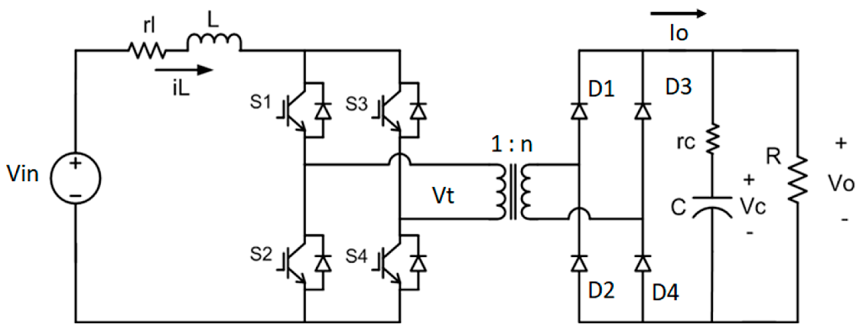
Figure 2.
Phase Shift Activation Diagram.
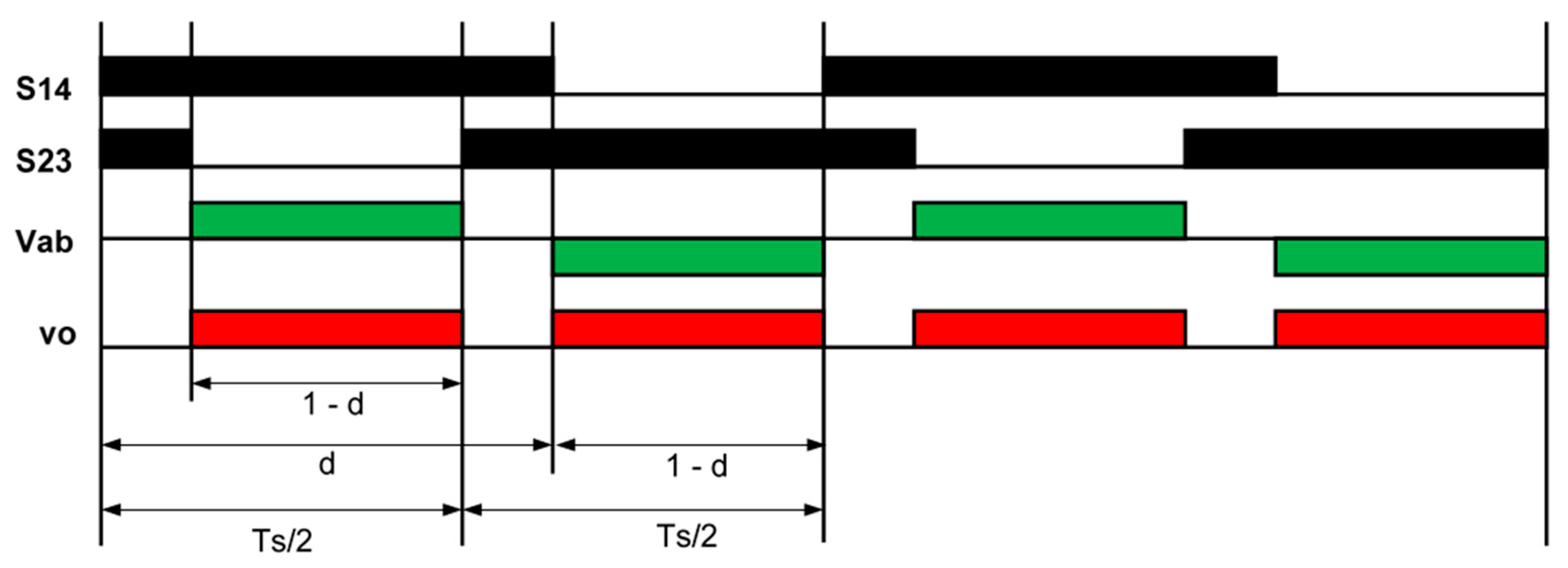
Figure 3.
Equivalent Circuits of Switch Cycle Performance.
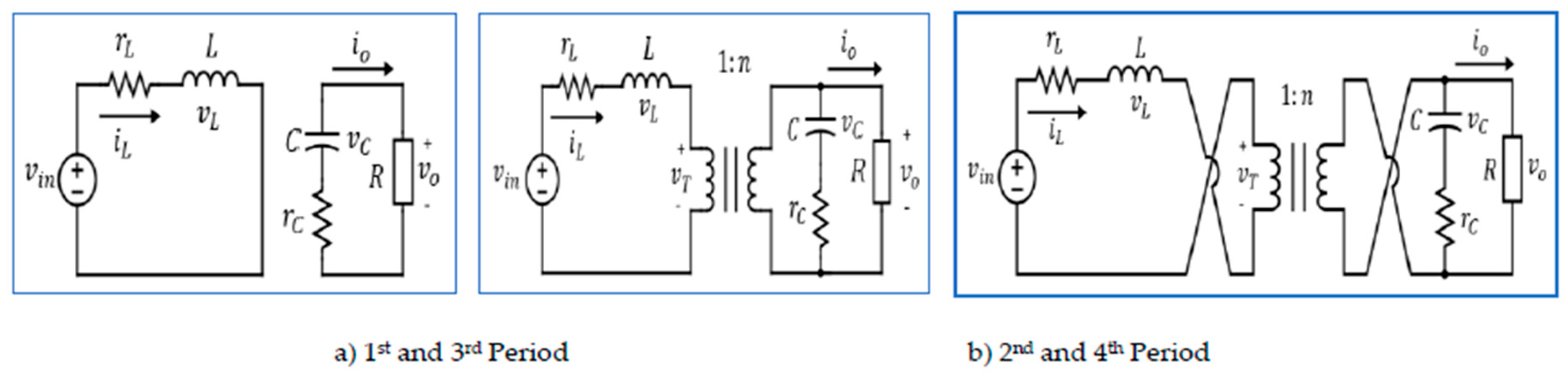
Figure 4.
Schematic of Closed-Loop System with PID-LQR Approach.
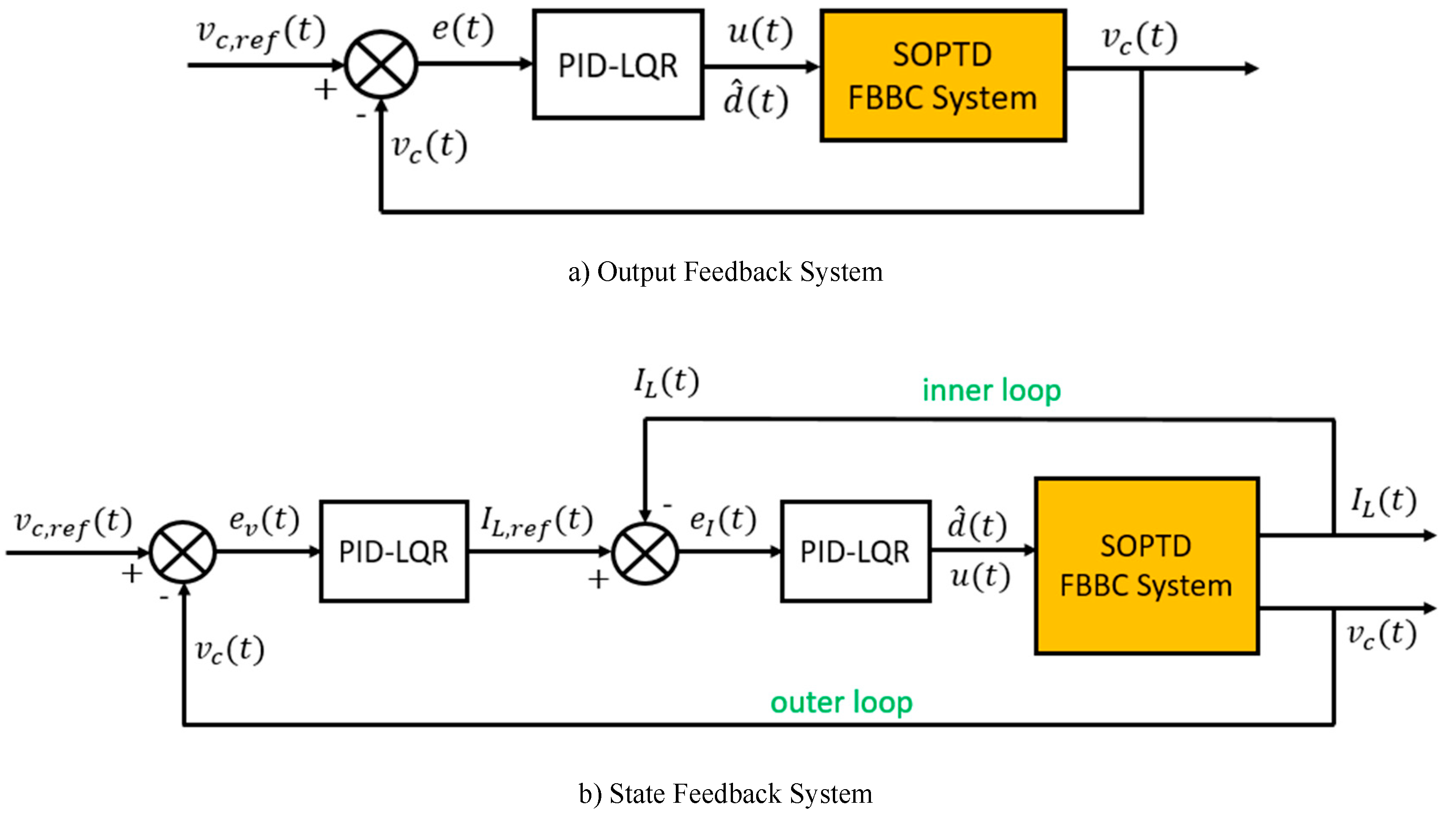
Figure 5.
Response Transient of the Open-Loop FBBC.
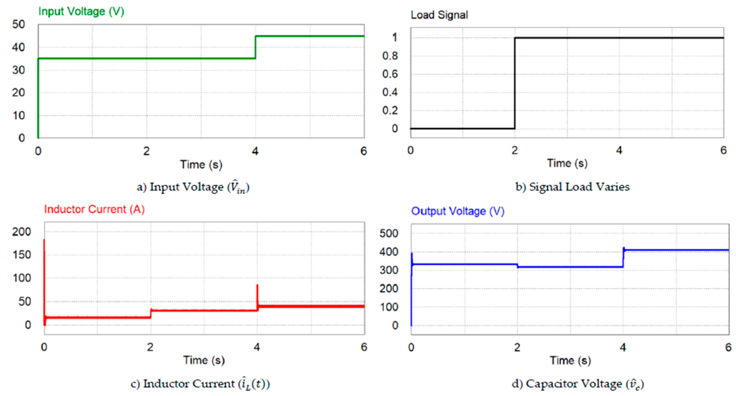
Figure 6.
Capacitor Voltage Response.
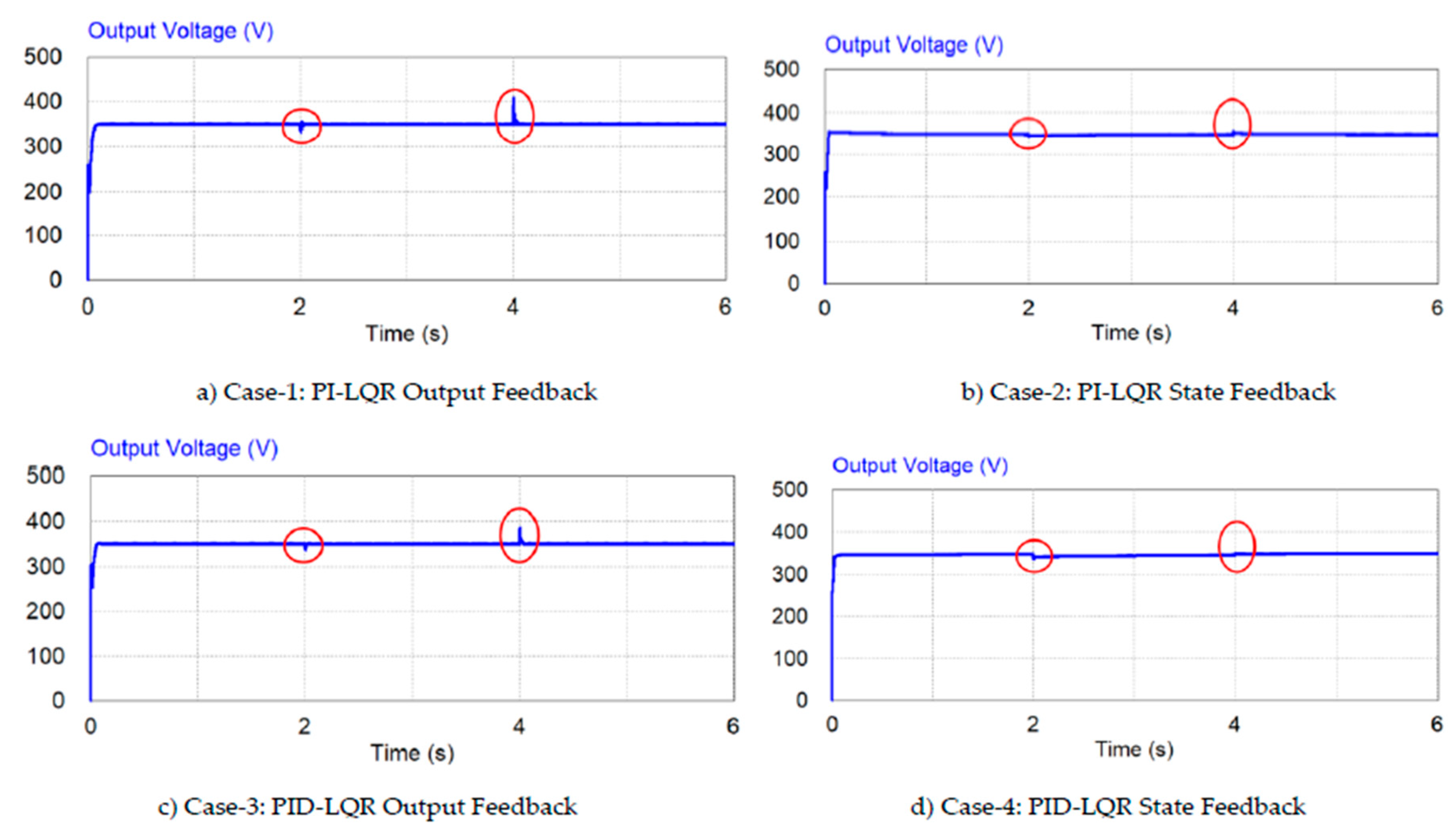
Figure 7.
Output Voltage Response during Load Changes.
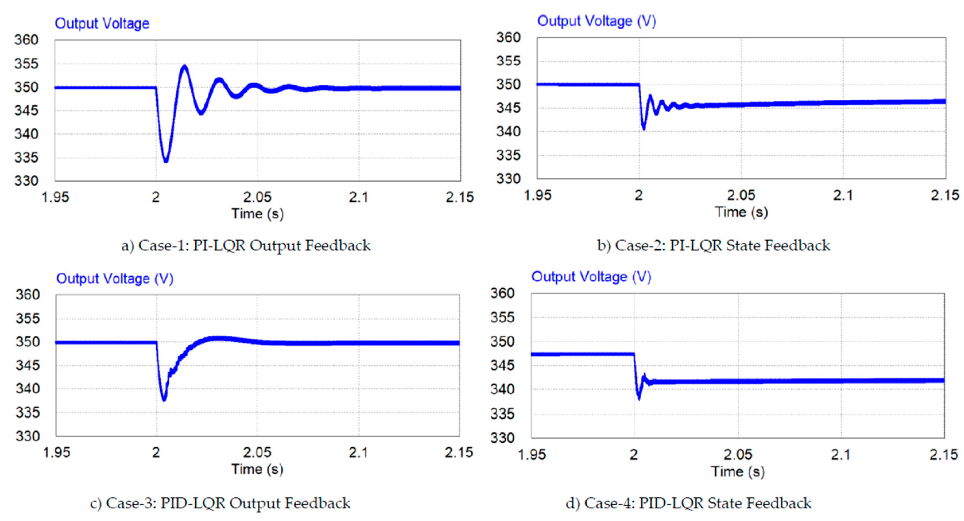
Figure 8.
Output Voltage Response during Input Voltage Changes.
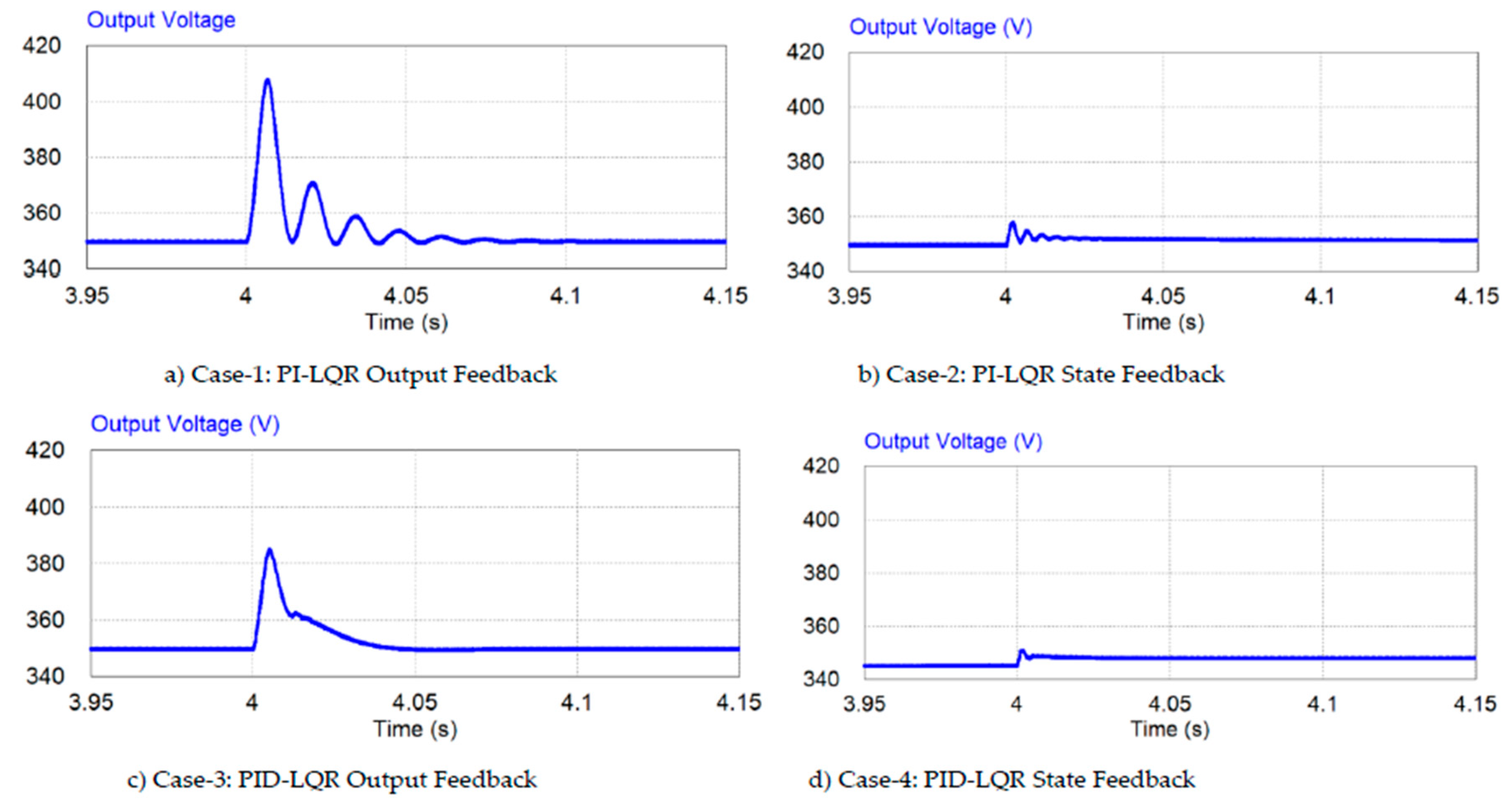
Figure 9.
Inductor Current Response.
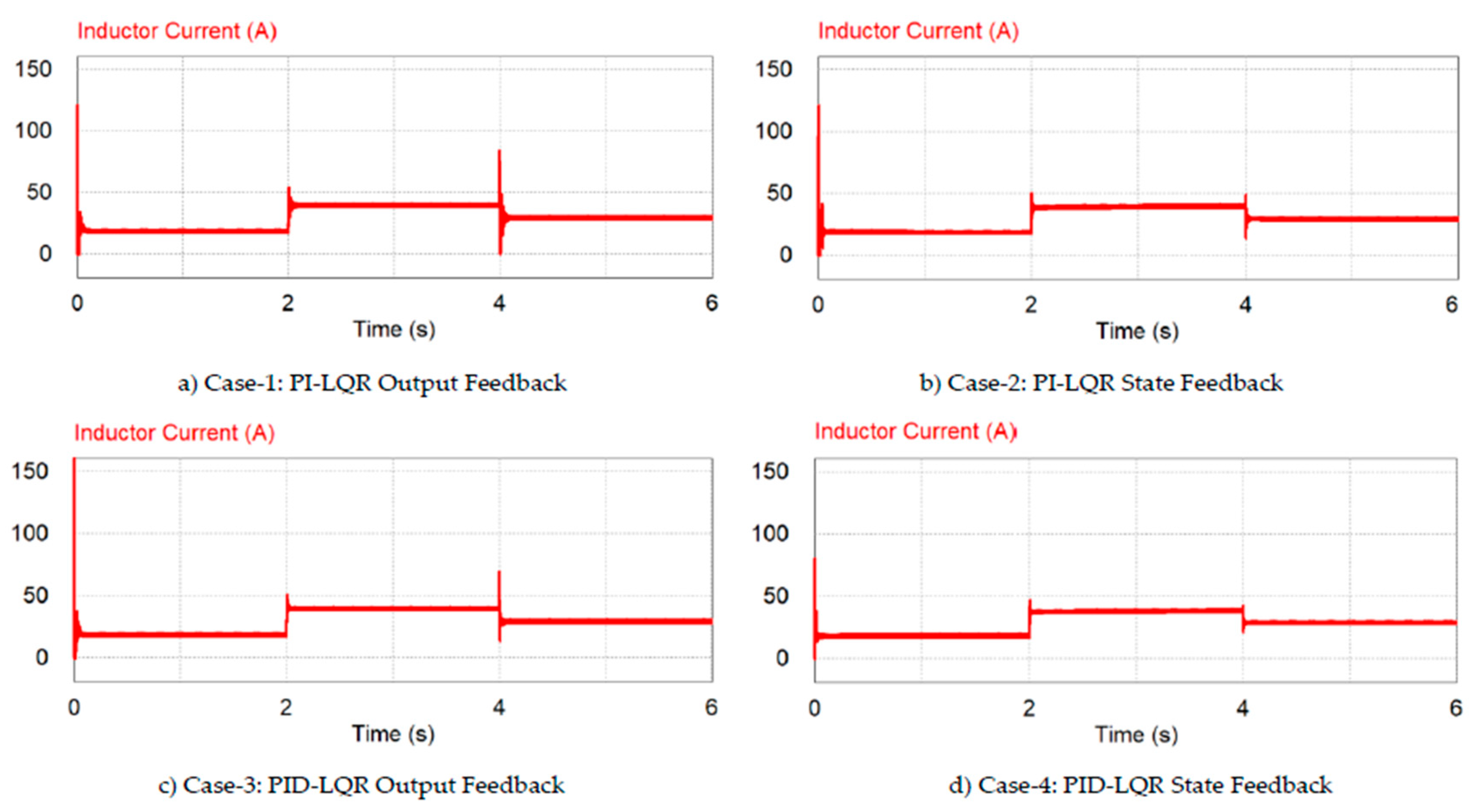
Figure 10.
Inductor Current Response during Load Changes.
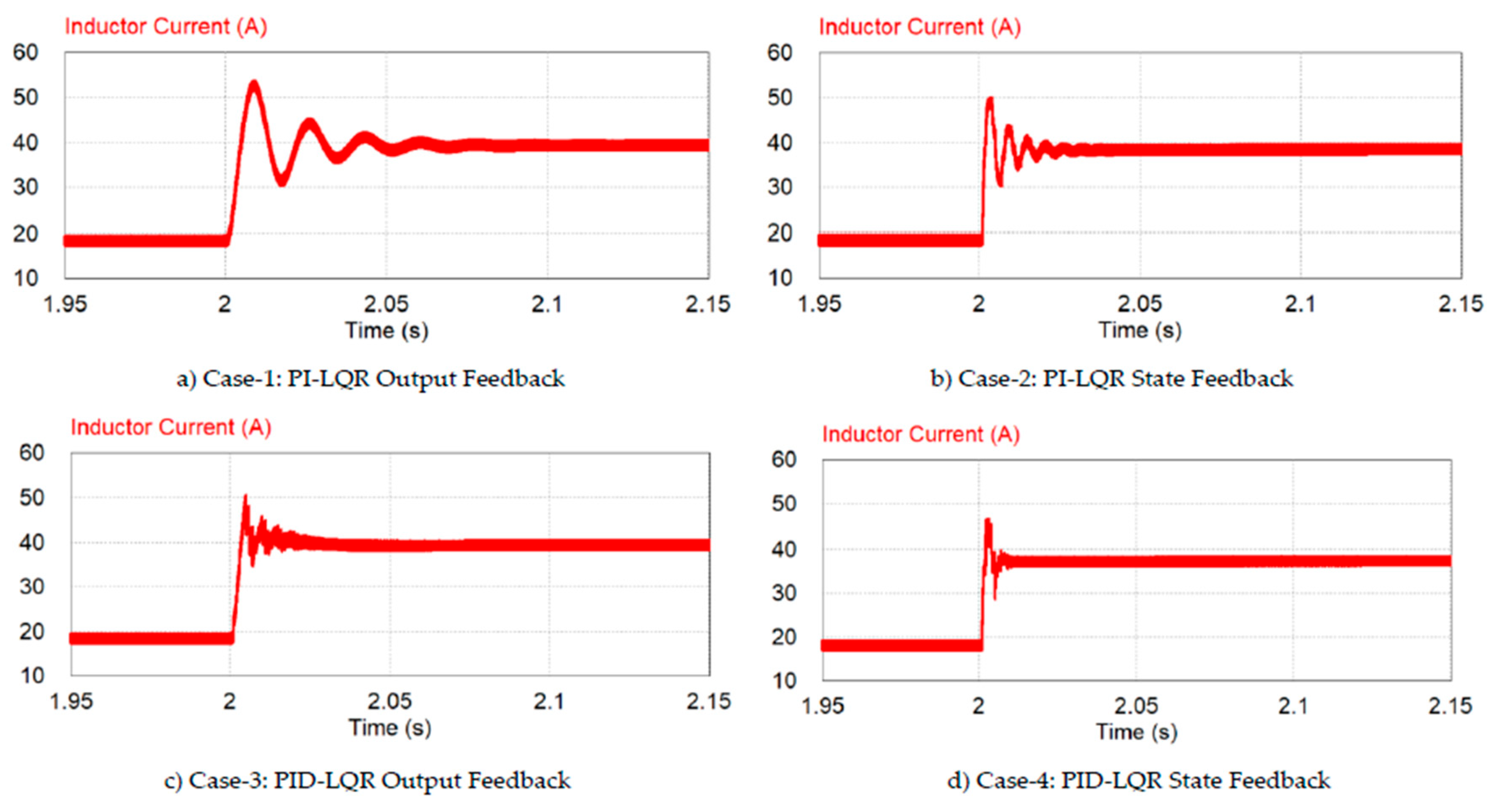
Figure 11.
Inductor Current Response during Input Voltage Changes.
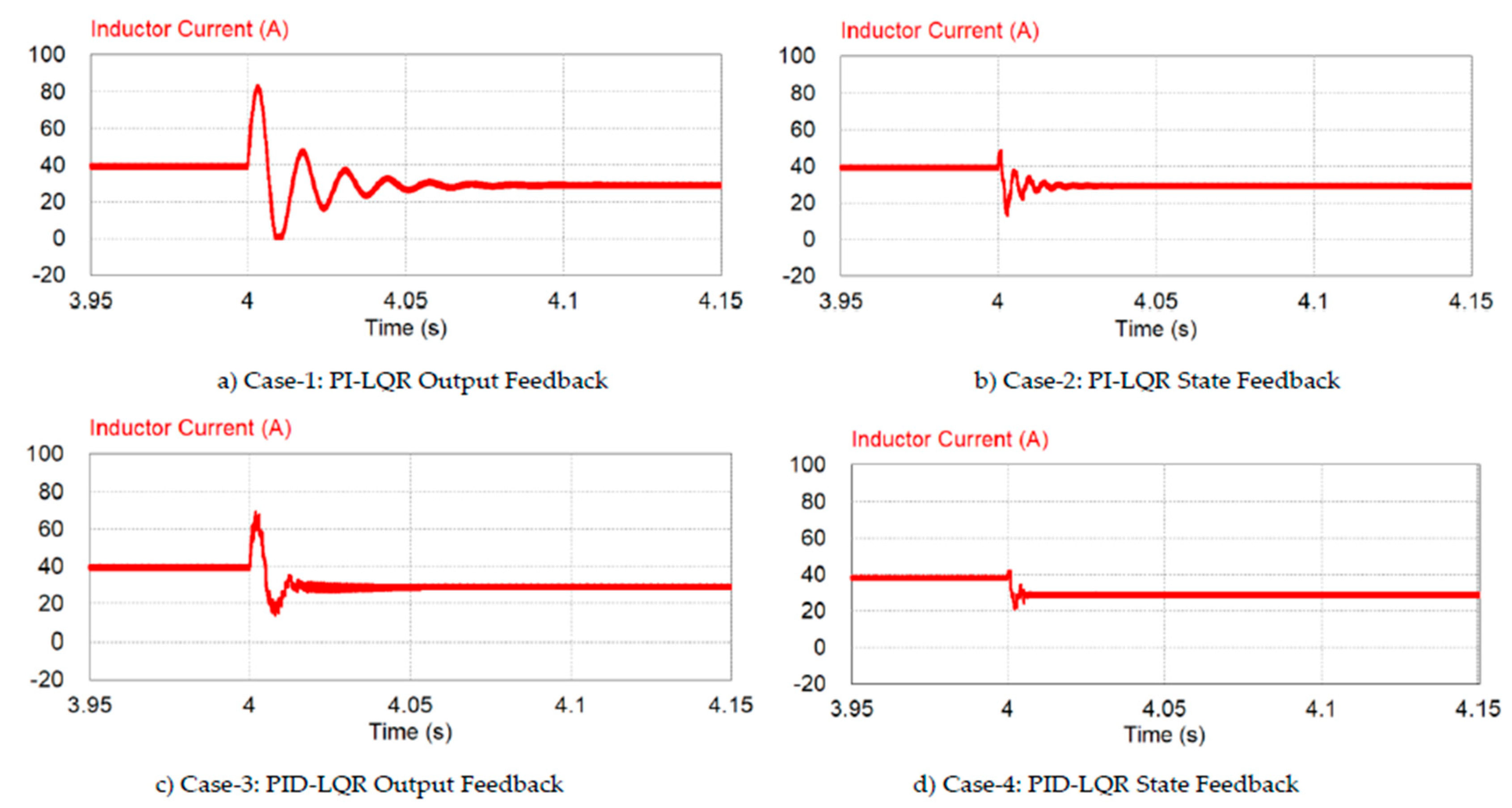
Figure 12.
Control Signal Response.
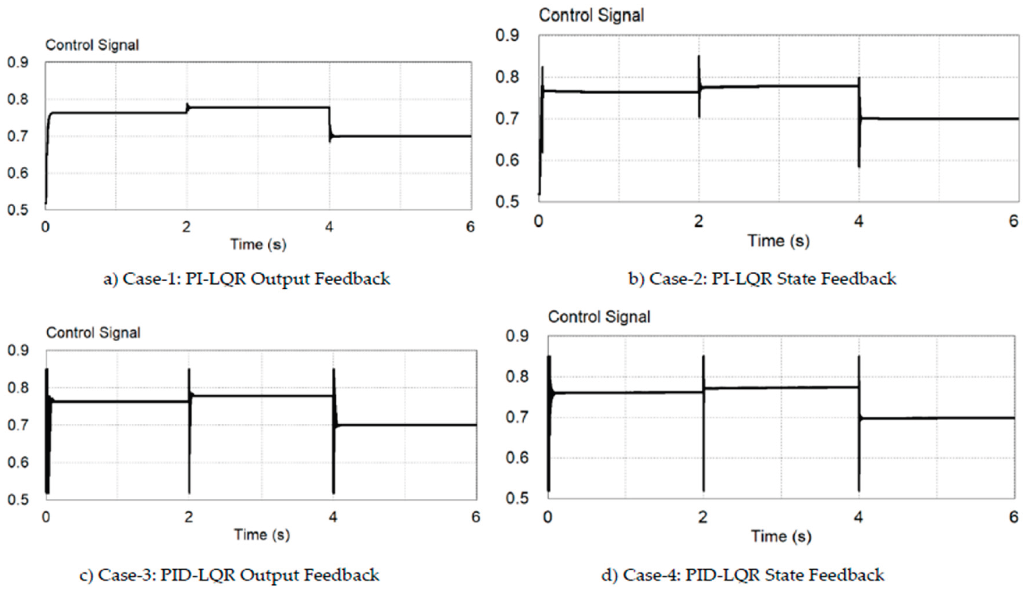

Table 1.
Parameters Component FBBC.
| Symbol | Description | Unit | Value |
|---|---|---|---|
| The Input Voltage | Volt | 35 | |
| The Output Voltage | Volt | 350 | |
| The Duty Cycle | 0.75 | ||
| The Full-load Resistance | Ohm | 100 | |
| The Half-load Resistance | Ohm | 200 | |
| The Switching Frequency | kHz | 10 | |
| The Capacitor | uF | 330 | |
| The Stray Resistance Capacitor | mOhm | 50 | |
| The Inductor | uH | 391 | |
| The Stray Resistance Inductor | mOhm | 100 | |
| The Inductor Current Nominal | Amper | 35 | |
| The Capacitor Voltage Nominal | Volt | 350 |
Table 2.
The control constants for cases 1 to 4.
| Cases | Outer Loop Capacitor Voltage |
Inner Loop Inductor Current |
||||
|---|---|---|---|---|---|---|
| Case-1: PI-LQR output feedback | 1.11 | 126.16 | ||||
| Case-2: PI-LQR state feedback | 4.32 | 9.19 | 0.01 | 1.13 | ||
| Case-3: PID-LQR output feedback | 1.92 | 194.15 | 0.142 | |||
| Case-4: PID-LQR state feedback | 3.30 | 1.09 | 0.01 | 1.911 | 0.03 | 0.01 |
Disclaimer/Publisher’s Note: The statements, opinions and data contained in all publications are solely those of the individual author(s) and contributor(s) and not of MDPI and/or the editor(s). MDPI and/or the editor(s) disclaim responsibility for any injury to people or property resulting from any ideas, methods, instructions or products referred to in the content. |
© 2026 by the authors. Licensee MDPI, Basel, Switzerland. This article is an open access article distributed under the terms and conditions of the Creative Commons Attribution (CC BY) license.
Copyright: This open access article is published under a Creative Commons CC BY 4.0 license, which permit the free download, distribution, and reuse, provided that the author and preprint are cited in any reuse.


