Submitted:
15 January 2026
Posted:
16 January 2026
You are already at the latest version
Abstract
Substrates have become essential enabling materials for creating lightweight electronic components, particularly supporting advanced telecommunication technologies. This progress is driven by continuous advancements in novel substrate materials and cut-ting-edge fabrication techniques, pushing the limits of high-frequency device design. This paper explores both the challenges and breakthroughs in 5G mmWave substrate technology, focusing on recent developments in materials, device fabrication and integration methods that enhance performance and providing an in-depth analysis on the importance of mmWave technology. This paper highlights the key concerns in substrates design to researchers and academicians accelerates invention and commercialization of substrate designs in areas such as antenna engineering and integrated circuit technologies as well as addressing key issues like scalability and thermal impact in flexible substrates. Since matters related to material losses and substrates’ fabrication constraints are increasingly severe at high frequencies, mmWave substrates are highly needed to be look at, therefore this paper details the particular issues related to mmWave propagation and manufacturing design processes for high-frequency devices. Aims at optimizing antenna and system reliability by employing advanced design and materials as well as outlines the existing gaps that need a clarification to augment 5G mmWave infrastructure and services.
Keywords:
substrates
; mmWave antenna design
; 5G substrate materials
; high-frequency dielectric characterization
1. Introduction
The coming of fifth-generation (5G) holds a great potential in providing an ultra-fast data rate, a very low latency and a significantly improved spectral efficiency by exploiting the millimetre-wave (mmWave) spectrum for the first time in mobile communication infrastructures as a requirement intended for a lot of emerging applications [1]. A number of studies [2] considered mmWave spectrum as a significant candidate for 5G services. At mmWave frequencies, systems are extremely influenced by the electromagnetic characteristics of substrate materials, therefore, accurate knowledge is vital for the finest and robust design of such systems. The unique traits of mmWave communications pose a range of obstacles that limit their full deployment, spanning integrated circuit and overall system architecture, interference control, spatial reuse, obstruction compensation, and adaptive system oversight [3].
Substrates, which can be either textured or uniformly flat, act as the foundational platform onto which conductive layers are subsequently applied [4]. The choice of substrate material is not merely a fabrication detail; it fundamentally influences device operation and end performance [4]. The authors in [5], for example, substituted a Rogers substrate in an antenna design and observed pronounced performance variation, which they correlated to the substrate’s dielectric constant and other mmWave parameters, a finding later validated by [6]. In selecting a substrate, engineers weigh a blend of criteria; electrical loss, machining precision, fabrication speed, and mechanical durability [7]. Consequently, substrate design must satisfy targeted performance metrics while also tolerating the chemical, thermal, and mechanical stresses imposed by the functional layers that are built on the top of them [8,9].
A number of mmWave studies have been identified in the literature [10]. These studies have addressed key issues pertaining to propagation behaviour, applications, mmWave technologies, design considerations encompassing environmental conditions, usage scenarios and operating frequencies [10]. Nonetheless, they do not offer an extensive examination of 5G mmWave substrates design [11]. Therefore, this paper surveyed 5G mmWave substrates design, challenges and measurement aspects, targeting the most recent technical developments and analysing potential upcoming research directions for the 5G mmWave substrates. Specifically, we focus on:-
- Recent development and research contributions towards mmWave communications.
- The mmWave substrate design challenges and measurement approaches for 5G applications.
- Substrate materials and the need for low dielectric constants and low loss tangents materials.
- Fabrication methods and key design considerations for robust, high-performance mmWave devices.
- Emerging technologies including MIMO, and machine learning for optimization with their associated security concerns.
- Significant recent research accelerating 5G mmWave substrate innovations.
- Future research directions and identifying gaps in mmWave substrate development.
The remainder of this paper is structured as follows. Section 2 provide review methodology, Section 3 and its subsections provide an overview of mmWave frequencies and their significances while Section 4 describes challenges of mmWave substrates. In Section 5, we discussed about the fabrication techniques of mmWave substrates and Section 6 we talk about thermal management in mmWave substrates. In Section 7, we study the electrical performance. A description of substrate’s mechanical stability is provided in Section 8. Section 9 covers various hybrid mmWave substrates materials. Finally, Section 10 and Section 11 conclude the paper, which paves the path for future research, respectively.
2. Review Methodology
This review followed a systematic approach to identify, evaluate, and analyses recent studies related to mmWave antenna and substrate design for 5G. The process involved literature search, selection, data extraction, and normalization to ensure the inclusion of high-quality and relevant publications.
2.1. Literature Search and Databases
The literature search was conducted across several reputable scientific databases, including IEEE Explore, Science Direct, Springer Link, Scopus, and MDPI. Complementary searches were also performed using Google Scholar to capture additional relevant works not indexed in the above databases. The search strategy combined keywords such as “mmWave antenna design,” “5G substrate materials,” “graphene-based antennas,” “SIW technology,” and “high-frequency dielectric characterization.”
2.2. Publication Time Frame
To ensure relevance to current technological advancements, the publication window was limited to studies published between 2018 and 2025, covering the rapid development period of 5G and mmWave technologies. Older but highly cited benchmark studies were included only when they contributed foundational information on substrate behavior or design principles.
2.3. Inclusion and Exclusion Criteria
The inclusion criteria focused on peer-reviewed journal articles and conference papers, studies presenting experimental or simulated antenna/substrate performance above 24 GHz (mmWave range), research emphasizing substrate material properties (dielectric constant, loss tangent, and thermal stability), and works describing practical 5G applications, such as MIMO, SIW, or graphene-based antennas. While exclusion criteria involved non-English publications, articles lacking quantitative performance data, review papers, patents, and unrelated low-frequency antenna and or substrate studies (<10 GHz).
2.4. Data Extraction and Normalization
Key information extracted from each paper included substrate type, dielectric constant (εr), loss tangent (tan δ), operating frequency, bandwidth, gain, and radiation efficiency. Data were normalized into consistent units (GHz, dBi, etc.) and categorized based on antenna type and application band. Where necessary, results were cross-checked across multiple sources to verify accuracy. The normalized dataset was tabulated to enable comparative analysis of substrate performance and to highlight materials demonstrating superior efficiency, stability, and suitability for mmWave and 5G applications. The flow diagram summarizing the review process is given in Figure 1.
3. Overview of mmWave Frequencies and Their Significances
The mmWaves refer to frequencies ranging from 30 GHz to 300 GHz, corresponding to wavelengths between 1 and 10 mm [12] see Table 1 and Figure 2.
In the of 5G context, mmWave commonly denotes the frequency band between 24 GHz and 100 GHz [13,14], as illustrated in Figure 3. These frequencies offer very high bandwidth while supporting exceptionally fast data rates. However, signals at these frequencies are more prone to obstruction by buildings, vegetation and rainfall, and are also more vulnerable to adverse weather due to their shorter wavelengths [1]. The mmWave bands are attracting significant research interest due to their potential to enable data rates approaching 10 Gbps, offer abundant bandwidth, support narrow beamforming, ensure high transmission quality and provide strong detection capabilities [12].
In recent years, mmWave frequency bands have attracted growing attention from academicians and researchers [15] due to their unique characteristics and a wide range of emerging applications as illustrated in Figure 4.
3.1. 5G mmWave
At present, billions of wireless devices are engaged in global voice and data communication, leading to a remarkable surge in data traffic [16]. In response, 5G mmWave technology emerges with advanced features and enhanced services [17]. Due to the global bandwidth shortage, wireless carriers have turned to the mmWave spectrum, an underutilized frequency range in broadband communications, particularly the 24 GHz to 100 GHz band now designed for 5G use [15] as it can be seen in Figure 5. Currently, numerous studies and researches efforts [15] are available in the literature, focusing on mmWave propagation in both outdoor and indoor settings, particularly in densely populated areas [16]. The 5G mmWave is currently less utilized band, its signals transmit extra data than lower frequency wave and can be integrated with MIMO antenna with the potential to offer a greater magnitude capacity compared to current communication systems [18].
3.2. Advancements in mmWave Technologies
Recent advancements in wireless communication have been driven by the emergence of mmWave technology, which enables high processing speeds and increased integration density in modern electronic systems [1]. As illustrated in Figure 6, mmWave is being adopted in a range of current and emerging applications, such as IEEE 802.11ad WiGig, satellite communications, automotive radar, and airport security scanners [19].
Over the last few years, there have been extensive studies aimed at developing mmWave antenna technologies to satisfy the performance requirements of 5G systems. Several works have proposed different designs targeting compactness, broad bandwidth, high gain, and MIMO compatibility. For example, [20] in Figure 7, reported a 28 GHz MIMO antenna employing machine learning (ML) methods to realize a 10.34 dBi gain and above 26 dB isolation, whereas [21] suggested an eight-port slot array for 5G mobile terminals as provided in Figure 8.
Researches such as [20] have contributed to the development of high-directivity, low-profile antennas with reconfigurable beamforming, circular polarization and low mutual coupling, enhancing integration into dense and portable devices. Material investigations by [22] identified low-loss substrates suitable for mmWave ranges up to 115 GHz, while [23] proposed a compact metamaterial-based antenna for 26 GHz. Further, [24] developed a square loop printed antenna with dual-beam support and high efficiency at 28 GHz see Figure 9.
Directional horn antennas by [25] have enhanced beamforming capabilities and feeding networks for Ka-band applications. [26] Introduced a differentially-fed broadband antenna array using multi-layer PCB technology, optimized for base stations. The study in [1] contributed a graphene-based liquid antenna capable of beam reconfiguration across multiple 28 GHz frequencies. Additionally, [27] demonstrated how 5G supports the integration of power IoT and Cyber-Physical Systems in smart grids. Furthermore, [28] developed an RSIW-based Antipodal Vivaldi Antenna with enhanced bandwidth, gain, and low signal loss, improving performance for 5G and radar systems. Likewise, [29] designed a 50 μm polyimide on-chip SIW antenna, achieving compact size, low dielectric loss, and high efficiency for mmWave and IoT applications. Together, these innovations advance compact, high-efficiency, and wideband solutions for next-generation mmWave technologies, they also collectively address key challenges in mmWave propagation, offering scalable and high-performance antenna solutions for next generation 5G communication systems, as outlined in Table 2 in which a Cost Index (CI) on a 1–5 scale was used to compare mm Wave designed device costs based on weighted factors of material price, fabrication complexity, and availability, offering a transparent and consistent method to classify costs as low, moderate, or high without relying on variable market prices.
3.3. Role of Substrates in mmWave Technology
Substrates provide the necessary physical environment and structural support for the circuits to operate effectively at mmWave frequencies. For the mmWave, substrates are important elements to support the signal propagation, thermal dissipation, mechanical reliability, component integration and environmental stability, as well as the compatibility with the fabrication process [35]. Substrate technology is also essential for implementation of the 30-300 GHz mmWave communication systems [36]. Substrate design generally involves the combination of different materials having different properties in order to achieve both good high-frequency electrical performance and good mechanical and environmental stability [36]. The role of substrates in mmWave technology is shown in Figure 10.
3.4. Types of Substrates Prevalently Used in 5G mmWave Systems
According to [37], substrate divides into discrete and integrated. Discrete substrates are usually insulators, while integrated substrates are, of course, semiconductors [36]. Discrete substrates therefore have a lower dielectric constant than integrated substrates, providing better electrical properties for passive components, especially in the RF and mmWave domains [37]. Various substrate fabrication methods yield substrates with distinct characteristics and they are typically categorized based on the materials employed and the techniques used in their production [36]. Despite significant early advancements and innovations, the field of 5G mmWave substrates still faces numerous challenges before achieving widespread practical adoption, presenting substantial opportunities for further scientific research and development, see Figure 11 [35].
3.4.1. Laminate Substrates
Laminates substrates are essential in mmWave, as their dielectric characteristics are of paramount importance during the layout for circuit and subsystem design [38]. However, this type of substrates suffer from cost inefficiency, with negative trade-offs for both materials and fabrication [36]. Full spectrum based measurements on several of these materials have been performed using different techniques and spreading from the low to the very high frequency, providing valuable data for engineer designing up to THz frequencies [38]. There are two typical laminate substrates used for the fabrication, FR-4 and Duroid. The properties of Duroid such as efficient uniform transmission of high-frequency signals and negligible signal loss, thermal problems make it an ideal candidate in new generations of communication devices. The study in [39] introduced a design strategy of low-loss, low-permittivity dielectric laminate substrates for microwave and mmWave frequency systems using mixing theory.
3.4.2. Ceramics Substrates
Ceramics are very attractive substrates for low-loss mmWave frequencies and can see increasing usage due to their appealing features. For example, Alumina Ribbon Ceramic (ARC) has been reported for 5G mmWave patch antennas that have low loss and small design and is applicable for mobile [40]. The authors in [41] presented the dielectric properties of a novel ultralow temperature co-fired glass ceramic composite proposed as a dielectric substrate for mmWave applications. Advantages of the ceramics substrates are stability, low signal loss, accurate line widths, high thermal conductivity and both heat and cold resistance. Usually, they are characterized as thin-film, thick film, low-temperature co-fired and high-temperature co-fired ceramics [36].
3.4.3. Organic Based-substrate Materials
Organic substrates are fundamentally lamina formed of organic-based composites layers [37]. On the other hand, they show favourable electrical properties and low-cost fabrication [7] but are considered to be enormous challenge on dimensional precision and surface roughness [7]. A liquid crystal polymer (LCP) is a well-known example of organic laminates with excellent properties at mmWave [42]. For example, the dielectric constants of LCP materials fall in the 2.0 - 4.5 range at frequencies within 140-220 GHz, and some exhibit nondispersive performance [43]. [44] designed a conformal ultra-wideband MIMO antenna on LCP substrate for 5G and mmWave IoT applications. Cyclicolefinpolymers (COPs) and polymer-ceramic composites are other organic substrates [37]. The authors in [45] also proposed an innovative multicore PCB and organic substrate method for the realization the broadband dual-polarized antennas at 28 GHz and 39 GHz for 5G mmWave communications.
3.4.4. Other Materials Substrates
At mmWave frequencies thin-film substrates such as glass or sapphire and hybrid, composite and flexible substrates can be used [36]. Glass, primarily containing amorphous silica (SiO2), amorphous substrate possessing low loss tangent as well as low CTE and is suitable for high frequency applications [36]. Sapphire, which is a single-crystal form of Al2O3 with hexagonal crystal structure, has similar advantages to alumina but with better surface smoothness, in many cases rendering it the ideal choice. In Figure 12, the main classes of substrates appropriate for mmWave communication are presented.
3.5. Key Properties and Requirements for mmWave Substrates
Selecting a substrate for mmWave applications is currently a major challenge for academicians and researchers. For instance, [5] extensively investigated how different substrate dielectric materials affect the performance of a wideband magneto-electric dipole (MED) phased array antenna, utilizing four commercially available substrates for mmWave applications. Their study offers a foundational insight into how dielectric properties influence substrate performance and serves as a valuable reference for selecting suitable dielectric substrates for 5G mmWave systems. In order to attain high speed data transfer from the device to device with minimal error, employing materials of low dielectric constant (εr) and dissipation factor (tan δ) should be regarded as a main factor. Recently, numerous low εr and tan δ materials have been suggested, for example, modified polyimide (MPI), epoxy, polyphenylene ether (PPE) and polybenzoxazole (PBO). Nevertheless, the dielectric properties and moisture stability of the aforementioned materials are inadequate for high speed applications [46]. Therefore, achieving high signal integrity and low transmission delay at high-frequencies has directed academic and research efforts toward developing interlayer dielectric materials with low εr and tan δ [47].
Similarly, to construct mmWave systems effectively, the substrate material should possess a low εr [48], as a lower εr reduce capacitance, minimizing crosstalk from capacitive coupling [48]. It also facilitate faster signal transmission through the substrate, enabling higher data rates and reduced latency [22]. As well, a low tan δ ensures minimal signal attenuation in passive components and supports highly-efficiency antenna performance [49]. These low-loss dielectrics allow to integrate high-quality off-chip elements like inductors, filters, resonator in the first Redistribution Layer (RDL) [50]. In addition, the low tan δ values reduce the inherent high attenuation at mmWave frequencies, leading to the acceptable signal transmission inside devices [22]. These low-loss dielectric facilitate integration of high quality off-chip components such as inductors, filters and resonators in the first redistribution layer (RDL). Furthermore, by lowering the tan δ values, any naturally high attenuation at mmWave frequencies can also be suppressed to ensure sufficient transmitting of signal in the devices.
3.5.1. Dielectric Constant
The dielectric constant (εr), commonly known as the relative permittivity, describes a material’s atomic-level response to an electric field and is normally in the range 3-4 for discrete substrates [36]. With a growing tendency, εr’ s role is also growing in the behaviour of materials [36]. Materials with lower dielectric constants allow for faster signal propagation and reduced attenuation [36]. Thus, in order to achieve an efficient mmWave operation the substrate should be homogeneous in terms of dielectric characteristics throughout its body [36]. Different studies [51] have explored the influence of εr on devices performance for 5G mmWave applications. Ermis, 2024 investigated the influence of substrate εr and thickness for 5G application on a 38 GHz rectangular microstrip antenna. Similarly, [52] analysed a microstrip patch antenna at 28 GHz with various dielectric substrates. In addition to these, [22] introduced a full characterization of dielectrics for the selection of 5G mmWave candidates.
3.5.2. Loss Tangent (Dissipation Factor)
The loss tangent (tan δ) or dissipation factor quantifies dielectric losses in substrate materials, and it is another important factor besides εr [36]. Reduced tan δ helps to lower the attenuation in transmission lines for better performing signals [36]. In addition, the quality factor of dielectric is the reciprocal of tan δ that indicates its efficiency at high frequency [36]. The authors in [53] investigated the effects of tan δ and conductive surface roughness in transmission line losses of 5G mmWave frequency. They showed that conductor loss is dominate in thin substrate and also indicated the advantages of low-roughness copper foil. The entire dielectric characterization of several materials 5-115 GHz showed εr and tan δ to be approximately constant, such that it grows linearly with frequency [22]. There are many studies on the impact and improvement of tan δ in substrate materials for 5G mmWave applications. For instances, [54] studied the influence of dielectric properties on the performance of a 5G planar branch line coupler. [55] as well, reported a new low-loss dielectric material at 10 GHz. Likewise, [56], created a low tan δ adhesive for reducing transmission losses in mmWave substrates. Equally, [57] reported a newly developed dielectric material with tan δ < 0.003 at 39 GHz, applicable in 5G mmWave RF modules.
3.5.3. Electrical Conductivity
Electrical conductivity (σ), the reciprocal of resistivity, is a consequence of free electrons in the atomic structure of a material [36]. In substrate design, conductivity is highly required, especially in metallic layers, but also significantly affects semiconductors behaviour [36]. There has been extensive research aimed at σ measurement in 5G mmWave substrates. The authors in [58] developed a broadband measurement approach using a balanced-type circular disk resonator (BCDR) for assessing σ and εr from 20 GHz to over 100 GHz. Their findings indicate that as temperature and frequency increase, substrate tan δ rise while σ decreases. [53] examined loss properties of different transmission lines, finding that conductor loss dominates in thin substrates and low-roughness copper foil is effective in reducing losses. The authors in [59] measured the electrical parameters including σ of materials used as substrates for wearable antennas in 5G frequency bands. [60] introduced a low-loss dielectric material for 5G RF modules, demonstrating superior electrical reliability and filter performance in the mmWave frequency range.
3.5.4. Skin (Penetration) Depth
The skin depth is a frequency-dependent property that significantly affects the selection of metallization in substrates. It refers to the phenomenon where, at high frequencies, RF currents are confined primarily to the surface layer of a conductor, rather than flowing through its entire cross-section [36]. The study in [61] presented a scheme to design electromagnetic wave (EM) absorber based on Ni deposition that forms sub-skin depth periodic patter which induces resistive (rather than reflective) properties on the structure, which results in enhanced absorption of EM wave.
3.5.5. Thermal (Heat) Properties
Thermal properties are vital on the design of mmWave substrates since heat density increases with the frequency. Important thermal properties are thermal conductivity (the material’s ability to conduct heat, often large in materials with a lot of free electrons, e.g., diamond, TPG, CNTs) and thermal expansion, which is measured by the thermal expansion coefficient (CTE) [36]. To inhibit thermal mismatch, one would design effective substrates with low CTE or with compatible component materials. With low CTE, the materials such as laminates and TPG [36] are recommended for high frequency applications. Studies recently performed have carried out a thorough investigation on the thermal properties of mmWave substrates focusing their reliability and conductance capability at different thermally disparate environments. The paper in [62] have shown that the hybrid substrates outperform the FR-4 in terms of thermal reliability for mmWave modules. Another paper in [63] demonstrated that β-Si3N4 is an excellent substrate for heat dissipation with decent thermal conductivity as well as good dielectric properties for wireless communication. The work in [64] have also shown the influences of loss tangents and conductivity on the propagation of microstrip line with the increase in temperature and frequency. Additionally, the authors in [39] designed a low-loss, low-permittivity dielectric substrate with superior electrical performance on Maxwell Garnett mixing theory for high-frequency-related applications.
3.5.6. Dielectric Breakdown (Insulation Failure)
Dielectric break down is a critical property of substrate materials, defined as the voltage threshold at which an insulating material begins to conduct electricity due to excessive electric field strength. When this threshold is exceeded, current flows through the dielectric, compromising its insulation capability [36]. In the context of mmWave 5G systems, the authors in [5], studied how dielectric substrates influence the performance of magneto-electric dipole phased array antennas, while the authors in [38,65] characterized the dielectric behaviour of common substrates to evaluate their suitability for high-frequency applications.
3.5.7. Reliability and Mechanical Stress Factors
The reliability of the electronic system generally refers to their ability to function consistently over time without failure [36], In the context of substrates, reliability is more specifically associated with a material’s capacity to withstand stress and strain. Stress reflects internal forces, while strain results from external loads. Young’s modulus, defined as the ratio of the tensile stress to the tensile strain, quantifies a material’s resistance to deformation [36]. The study in [66] investigated the reliability of mmWave modules under thermal cycling, linking solder joint failures to substrate warpage. Later, the authors in [62] found that mmWave modules built on hybrid substrates showed superior reliability under temperature stress compared to those on conventional FR4 substrates.
3.5.8. Additional Substrate Characteristics
Other important substrate characteristics include thickness, glass transition temperature, decomposition temperature, flammability, moisture absorption, chemical resistance and surface roughness [36]. As shown in [67], glass substrates demonstrated low dielectric loss and smooth surfaces, making them promising candidates for 5G and mmWave applications.
3.6. Advancements in mmWave Substrates
Recent advancements in mmWave substrates show a clear move toward tunable and high-performance materials. Currently, a wide range of mmWave devices have been developed using different substrate materials to meet the demands of 5G applications [68]. Several studies, such as those by [69], explored microscript patch antennas fabricated on Rogers RT/Duroid-5880, FR4-epoxy and Rogers RT5880, respectively, highlighting with both low-cost and high-performance options based on their varying εr and tan δ. Moreover, studies by [70] proposed an array of MIMO antennas with various substrates such as FR-4, Rogers RT5880, RO5880, Duroid-5880 and RO4350B to achieve a high gain, isolation and broad bandwidth. These works affirm that by proper selection of substrate and optimized antenna geometries compact and high gain 5G mmWave system is realized. In addition, [71] further verified the favourable performance of Rogers RT5880 for low-loss antenna designs, and [72] proposed the employment of barium fluoride (BaF2) ceramics to mmWave applications based on LTCC technology.
Similarly, the study in [1] introduced a graphene-based liquid antenna on an LCP substrate achieving 360° beam reconfiguration and about 7 dBi gain at 28 GHz, highlighting flexibility and reconfigurability.The authors in [73] also used a bilayer graphene film substrate enabling frequency tuning between 29.6–40 GHz with low reflection losses, proving graphene’s potential for adaptive mmWave systems. Meanwhile, [20] utilized a Rogers RT/Duroid 5880 substrate for a 28/38 GHz MIMO antenna achieving high isolation and wide bandwidth. Together, these studies demonstrate that combining traditional low-loss substrates with emerging graphene-based materials enhances mmWave antenna performance, tunability, and efficiency for 5G applications.
Furthermore, [46] developed advanced thermosetting siloxane-hybrid substrates with low dielectric constant, low loss tangent, and high stability under humid conditions, enhancing performance and reliability for mmWave microstrip lines and filters. Meanwhile, [74] focused on accurate dielectric characterization at terahertz frequencies, enabling precise evaluation of substrate permittivity and losses using THz measurement techniques. Together, these studies advance mmWave technology by improving substrate material quality and providing accurate data essential for efficient high-frequency antenna and circuit design. [75,76] demonstrate significant advancements in mmWave substrate applications for MIMO antenna systems by designed a 5×20 massive MIMO antenna using a low-loss Rogers RT/Duroid 5880 substrate, achieving high gain, wide bandwidth, and excellent isolation, key for 5G base stations and developed a 2×2 MIMO antenna array optimized on a low-dielectric, high-stability substrate, delivering improved radiation efficiency, compactness, and reduced mutual coupling, respectively. Collectively, both studies highlight how selecting low-permittivity, low-loss substrates greatly enhances MIMO antenna performance, enabling efficient, high-speed mmWave communication
The results carried out by the above authors demonstrate that a significant progress has been made in 5G mmWave antenna design and optimization of the substrate material. All mentioned substrates were selected based on the desired electrical and mechanical characteristics, and so, for instance, FR-4 was found to be preferable for an inexpensive, small size design with moderate performance and extremism Rogers and Duroid in the case of supporting high frequency application with a low loss, and a high gain and a wide bandwidth. Furthermore, BaF2 ceramics have been designed for LTCC applications with higher Q values, lower sinters, better bonding to metal and polymer. Moreover, for 5G and mmWave applications, substrates with low dielectric constant and minimal loss are ideal. Rogers RT/Duroid 5880, RO4350B, Arlon Diclad 880/527, and CLTE-MW offer excellent performance due to their low dielectric permittivity (≈2.1–3.5), low loss tangent (≈0.0009–0.003), and high thermal stability, making them highly efficient at 26–60 GHz. Graphene adds advantages of tunable conductivity and flexibility for reconfigurable antennas, while BaF2 provides very low permittivity and loss, suitable for ultra-high-frequency designs. In contrast, FR-4 and FR-4 epoxy, with high losses and unstable dielectric behaviour, are unsuitable for mmWave systems. Overall, Rogers-, Arlon-, CLTE-MW-, and graphene-based substrates are the most suitable for high-performance 5G antenna designs. A summary of advances in mmWave substrates in antenna applications is given in Table 3.
4. Challenges of mmWave Substrates
4.1. Design Challenges of mmWave Substrates
In the case of the mmWave system, the choice of low εr and tan δ substrates is an essential part for achieving wide bandwidth and low signal loss [11]. In mmWave system design, the use of substrates with low εr and tan δ is essential, if one wants to obtain broader bandwidth and lower signal loss [11]. Despite these many benefits, mmWave communication remains fraught with certain technical issues such as high pass loss, atmospheric attenuation, signal blockage, interference and lack of spatial reuse [3]. Non-technical obstacles are the high cost of infrastructure and low user digital literacy [3]. The study by [86] highlighted issues like narrow beamwidth and high directivity due to the short wavelengths of mmWaves. Accurate channel modelling is necessary for effective deployment, as signal generation, reception and propagation remain difficult at such high frequencies [87]. To address these, [88] recommended using the directional antennas with enhanced gain at both transmitter and receiver ends.
4.2. Challenges in Achieving High Precision and Quality
The mmWave transmission faces more several challenges than traditional low GHz radio frequencies due to its high propagation loss and limited link range. These difficulties arise from both propagation characteristics and technical constraints. The study in [36], identified key issues including transceiver design complexity, high fabrication costs, reduced passive component performance at high frequencies, impedance matching requirements and inadequate packaging. Although significant research efforts aim to reduce fabrication costs, additional problems remain [36]. The authors in [12] noted that, mmWave substrate design incurs high mechanical manufacturing costs and faces efficiency losses due to the extreme frequency spectrum. Further challenges include manufacturing tolerances and process reliability, which affect system performance [12].
5. Fabrication Techniques
Flexible electronics are rapidly advancing due to innovations in functional materials and fabrication methods, enabling the creation of uniquely shaped, cost-effective devices [35]. The emergence of 5G has further driven the development of RF devices operating at mmWave frequencies for use in wireless communication, automotive radar, high-resolution imaging and gigabit networks [7]. These applications demand compact, high-density, low-loss and cost-efficient system integration [7]. Therefore, substrate selection must consider factors like electrical loss, machineability, yield and mechanical stability [7]. For instance, [89] illustrated the gains of deep-learning-aided substrate shaping in mmWave communication systems utilizing dielectric resonator antenna configurations.
5.1. Various mmWave Fabrication Techniques
The section presents a review of various techniques such as: mmWave coating and chemical deposition; sputtering; and a variety of patterning and shaping techniques such as photolithography, 3D printing, fabrication over mould, and new integrated techniques including hot pressing for design or modification of substrate structures.
5.1.1. Composite Techniques
- Coating technique
Methods of coating such as “spin-coating” involve depositing a particle containing liquid mixtures onto a flexible substrate with apparatus such as brash or machine work and can be subsequently exposed to heat or allowed to dry to form uniform composite thin films [90]. For example, [91], have successfully produced a FeSiAl/WS2 soft magnet composite, which is a uniform coating of the micrometre-scale WS2 sheets on the FeSiAl grains, it is a typical low eddy current loss and medium effective magnetic permeability composite, and is of high value for high-frequency applications.
- Chemical deposition technique
Chemical deposition includes the deposition of metals or oxides on flexible substrates by chemical solution from a chemical liquid under vacuum for the formation of a thin conductive film [90]. For instance, [92] prepared a magnetic polydimethylsiloxane (PDMS) hydrogel with chemical precipitation; the PDMS hydrogel was immersed into Fe2+/Fe3+ solution, and then processed to uniformly disperse magnetic nanoparticles in film.
- Sputtering technique
Sputtering is a thin-film deposition technique where high-energy particle bombard a target material in a vacuum, ejecting atoms that are deposited onto a substrate [90]. It enables the easy deposition of metals, alloys and compounds [93]. For example, [94] magnetron sputtering to deposit a 5 nm tantalum layer onto pre-stretched PDMS. Upon release, mismatched Young’s modulus cause surface wrinkling, which was then used to sputter a 150 nm FeCoTa film, creating a flexible magnetic layer.
5.1.2. Patterned and Structured Techniques
- Photolithography
Photolithography is a widely used micro and nanofabrication technique where patterns are transferred onto a substrate using photoresist and stepper tools, followed by etching to form microstructures, enables precise structures at nanometre to micrometre scales and includes variants such as soft, nanoimprint, e-beam, and scanning probe lithography [90]. For instance, [95] fabricated flexible 3D nanostructures like nanocoaxes on negative photoresist film through standard lithography stripping methods. The formed structures were chemically and mechanically stable, and hence appealing for wearable and bioelectronic applications. Similarly, [96] fabricated AgNW micropatterns based on PEG photolithography without universal etching, transferring on the hydrogels. The produced AgNW patterns exhibited good conductivity, flexibility and water stability, which show promise for use in next-gen bioelectronics devices and implantable devices.
- 3D printing techniques
The 3D printing technologies have been developed for manufacturing flexible electronic devices using conductive and resistive materials printed directly on flexible substrates including polymers, papers and silk [90]. Of these, FDM is one of the most popular, using extrusion of heated thermoplastic polymers, with resolution determined by the size of the nozzle (Pan et al., 2024). For example, [97] applied FDM to fabricate flexible sensors, including a composite of polyvinylidene fluoride and cobalt ferrite, showing satisfactory both electrical and mechanical properties for wearable purposes. Direct writing methods can be employed for the creation of flexible metal circuits with high conductivity and flexibility as well [90]. The MXene inks as utilized by [98], printed pressure sensors for touchpads and water level monitoring on flexible substrates that can also act responsively and accurately. Yet another approach is Selective Laser Sintering (SLS), which builds structures by the layer-wise sintering of powder materials [90]. The authors in [99] fabricated a thermoplastic polyether block amide (TPE) and multi-walled carbon nanotube (MWCNTs)/Nanocomposite sensor for sensitive and reliable E-skin health monitoring. Moreover, [100] obtained the direct writing of interfacial reaction of Polyvinyl Alcohol (PVA) and AgNO3 as polymer-metal precursors for flexible circuits. Taken together, these methods indicate the growing potential of 3D printing and direct writing for fabricating customized, high-performance and economically friendly flexible substrates.
- Fabrication with moulds
Moulding processes offer a simple and convenient approach for the interfacing of multiple materials, e.g., polymers, silicone, or other elastomer in a reusable mold and subsequently cured in the desired shape and profile [90]. It can shape the flexible structure, such as substrate and soft robot unit, which has a defined shape, elastic-mechanical property, and surface smoothness [90]. Shaped structures of custom configuration may be produced by changing the mould design. For instance, [101] fabricated an earthworm-inspired slippage of micro-structure-molding diaphragm by earthworm displacement, and was guaranteed to have a significant 3D bi-directional deformation in the low magnetic field of 40 mT attributed to its segmentation radially magnetized validated structure. These could easily be adapted for integration with soft robotic systems. Similarly, [102], fabricated a fast-response soft actuator by using Ecoflex rubber mixed with NdFeB particles. The actuator can be fabricated into grippers with different shape sizes, which exhibit some features of ultrafast response time (<0.1 s), ultra large strain (<120%), long-term stability and high precision, and is applicable for the grasping objects of spherical and cylindrical shapes.
5.2. Integrated Techniques
5.2.1. Hot Pressing
Hot pressing is an inexpensive and easy process that can bond flexible base materials with electronic and conductive elements by means of controlled temperature and pressure with high precision flexibility electronic device [90]. Especially, it is a promising tool for modifying polymers and composites for improved physical properties [103]. The work in [103] also showed that hot pressing (HP) is an effective approach to enhance electrical and thermal conductivity of acid-treated polymer PEDOT:PSS films to a high level of 1500 S/cm, 1.11 W/mK, respectively, owing to the optimized microstructure, thus making the HP treated films be used as both flexible conductor and heat sink. The authors in [104] developed a biodegradable, paper-like flexible composite using cellulose and graphene nanosheets. After hot pressing, the nanosheets were embedded into the fiber network, resulting in high isotropic conductivity (~10 Ω sq-1), surpassing traditional conductive paper technologies. Therefore, hot pressing enhances material performance and supports the scalable, eco-friendly production of highly conductive and thermally efficient flexible electronics.
5.3. Other Fabrication Techniques
Other notable fabrication techniques for mmWave devices include the use of photoetchable glass (PEG) for creating substrate-integrated waveguide (SIW), as demonstrated by [105]. PEG’s photoetchable properties enabled the formation of through glass via (TGVs), making it suitable as a dielectric material for SIW-based 5G applications. Similarly, glass substrates with TGVs has been adopted for packaging substrates and interposers in high-frequency applications [106,107], supporting components like filters, antennas and waveguides [108]. Additionally, [109] discussed the use of high resistivity Fully Depleted Silicon-On-Insulator (FD-SOI) substrate for mmWave applications, focusing on material and fabrication challenges. Table 4 provides a summary of fabrication techniques for to creation of a flexible devices. A Cost Index (CI) on a 1–5 scale was used to compare fabrication technique costs based on weighted factors of material price, fabrication complexity, and availability, offering a transparent and consistent method to classify costs as low, medium to high, and high or very high.
6. Thermal Management
6.1. Heat Dissipation Issues in mmWave Substrates
Material properties also affect the thermal management of mmWave substrates, for which the majority of the solutions are passive, with the substrate materials being closely tuned. Low thermal dissipation can be detrimental for the performance and reliability of electronic systems. The temperatures can result in electrical property changes which cause signal integrity problems, timing delays and failure. Excessive operating temperatures shorten the life of electronic components, degrades solder joints, and increases potential of catastrophic failures. Decent heat dissipation performance is a crucial prerequisite to maintain normal operation level, low failure and operation time of electronic devices [110]. Some researchers paid more attention on the important issue of the heat dissipation in mmWave substrate and device and proposed advanced cooling and thermal management methods. Authors in [111] suggested a solution using Schottky diode integrated CVD diamond substrate to achieve improved heat dissipation and device power efficiency.
Another work presented in [62] demonstrated that hybrid substrates enhance the thermo-mechanical reliability of mmWave modules. Furthermore, in [101], the authors has been shown that AlN is much better than GaAs in enhancing the thermal characteristic of THz QCLs. Likewise, in [112], the authors idealizing 3% Mo as the AlN:Mo ceramics refined for a δ-function heat under W-band radiation. The work in [113] presented a transparent radiative cooler based on 4H-SiC and stacked layers for passive cooling. Similarly, the work in [114] had c-BN films for the improvement of LED cooling and they could decrease the temperature by 5-17 0C and increase the output by 27.9%. In conclusion, these reports highlight the importance of high thermal conductivity materials, hybrid substrates, and passive cooling methods in better heat dissipation of advanced electronics. The characteristics of included studies are presented in Table 5.
6.2. Methods for Improving Thermal Performance
Several studies [116] have investigated successful methods to improve thermal performance of 5G mmWave substrates. These techniques (summarized in Table 6) are designed to answer the critical heat dissipation issues and to enhance mechanical robustness and system reliability. By taking these methods into account and applying suitable design principles, Metal substrate PCBs can be engineered to provide efficient heat dissipation while ensuring reliability across a range of operating conditions.
7. Electrical Performance
7.1. Effects of Substrate Materials on Signal Transmission Loss
The signal transmission speed V at high frequencies is influenced by transmission loss and interlayer dielectric resin by [47]. Where c is the speed of light in a vacuum, k is a constant and εr is the substrate’s dielectric constant; lower εr results in faster signal propagation. Additionally, in high-frequency circuits, the dielectric loss tangent (tan δ) of the substrate also affects signal loss by [47]. Where α is the transmission loss and f is frequency; lower tan δ leads to reduced signal attenuation. Given signal speed and efficiency are closely related to the dielectric properties of copper-clad laminates [47].
Transmission of high frequency signal in PCBs is affected by problems such as the RC delay, crosstalk, energy loss and impedance mismatch, which makes difficult for PCBs to realize the miniaturization and signal integrity of performance [47]. To solve this problem, the development of interlayer dielectric materials with low dielectric constant and loss tangent is an important research topic. As highlighted by [47] can be reduced by molecular structure design and the introduction of functional fillers. Reduce εr and tan δ from molecular design as well as by introduction of functional fillers. Especially, carbon nanofillers are highly attractive, since we can easily control their dielectric properties according to morphologies, concentrations, and fabrication methods.
Various techniques have been proposed earlier for improving signal transmission at high frequency. For example, the study in [117] noticed that dissipation factor is the one that affects the insertion loss to a great extent and the dielectric constant has a smaller effect. The authors in [118] highlighted that reducing substrate loss is more effective with thinner dielectrics at lower frequencies. The silver-seed Semi Additive Process, as demonstrated by [119], yields smoother transmission lines that minimize conductor and overall transmission losses. Moreover, the authors in [120] showed that foam substrates provide the lowest signal loss and highest radiation efficiency and gain for antennas. Furthermore, [121,122] confirmed that silver-seed copper plating on low-loss rigid substrates enhances conductor smoothness, further reducing signal loss. Together, these findings support the development of efficient, high-performance substrates for high-frequency electronic systems.
7.2. Mechanism of Dielectric Energy Loss
Dielectric loss occurs when molecular polarization cannot keep up with the oscillating electric field. If the relaxation time matches or is shorter than the field’s, frequency loss is minimum [47]. However, when the electric field oscillates faster than the polarization can respond, energy is absorbed and dissipated as heat [47]. Interestingly, when polarization becomes entirely unresponsive to the field, loss again becomes minimal [47]. The complex permittivity (ε*) describes this behaviour, comprising a real part (ε’) representing dielectric constant and an imaginary part (ε”) representing dielectric loss as. Their ratio gives the dielectric loss tangent, [47].
Multiple studies have examined dielectric loss mechanisms in 5G mmWave systems, focusing on material characterization and loss reduction approaches. For example, authors in [53] emphasized that using low surface roughness copper foil significantly reduces conductor loss in transmission lines. In [22], authors conducted broadband dielectric characterization up to 115 GHz, identifying low-dispersion, low-loss materials suitable for 5G. In [56], authors introduced new dielectric materials with low dissipation factors and strong adhesion to smooth copper foils, achieving notable reductions in transmission loss. Furthermore, [60] developed low-loss dielectric specifically for 5G and 6G mmWave applications. Taken together, the results of these studies provide guidance for dielectric loss mechanism optimizing in high-frequency devices used in 5G wireless systems.
7.3. Signal Transmission Loss Reduction Procedures
Signal loss is one of the crucial issues in high-speed substrate, because it impacts negatively on system performance and reliability [123]. Conductor loss, dielectric loss, the skin effect, radiation loss, impedance mismatch and crosstalk are the main contributors. In order to solve these kind of problem, the selection of low loss dielectric materials and the refine of copper foil types, such as the reverse-treated or the very low-profile (VLP) foils, have a crucial role in conductor loss and signal integrity reduction at high frequency [124]. Several studies have proposed new mechanisms to combat the signal propagation losses in mmWave systems. In [125], authors proposed a novel contactless air-filled substrate integrated waveguide (CAF-SIW) band pass filter, in which the dielectric loss is suppressed by not using any dielectric materials and the multilayer integration can be realized. The work in [126] have recently proposed the thin-film integrated passive device (TFIPD) filters based on spiral inductors and metal-insulator-metal (MIM) capacitors, and it has also demonstrated low insertion loss and high return loss for 5G bands. Authors in [127] coated PCBs with SiCOx/SiOx and not only signal loss but also surface adhesion and thickness were improved. Additionally, [128] prepared epoxy-derived substrates with surface-modified aluminium flakes to enhance εr and reduce tan δ from 1 to 10 GHz. The paper in [129] produced flexible copper clad laminate (FCCLs) on polyimide based on direct metallization realized very low insertion loss (0.03–0.06 dB/mm up to 40 GHz), which outperforms adhesive counterparts. Authors in [130] implemented terahertz graphene antenna with a folded quarter wave transformer and obtained the high gain (8.65 dB) and almost the perfect radiation efficiency (99.8%). These works show that reduced loss at mmWave frequencies calls for an approach that integrates low-loss materials, careful structural design and advanced fabrication. Together, they emphasize the fundamental importance of material innovation, surface-engineering and architectural advancements for achieving the high performance required by future wireless systems such as 5G and terahertz systems. Table 7 Summarizing salient points from the referenced studies on methods of reducing signal propagation losses in mmWave substrates.
7.4. Impact of Conductor Roughness in 5G mmWave Substrates
Recent studies highlight that the rapid expansion of mmWave applications for 5G systems introduces significant design challenges, particularly due to conductor surface roughness, which degrades signal transmission and antenna performance at high frequencies. Research by [131] and [53] demonstrated that increased surface roughness reduces conductivity and elevates loss as the operating frequency approaches and exceeds 30 GHz. Low-roughness copper foils, such as VLP, have proven effective in minimizing signal loss in thin mmWave substrates. Furthermore, models by [132] and [133] show a strong, often exponential, dependence of conductor loss on roughness, emphasizing the importance of advanced fabrication techniques to ensure reliable, low-loss transmission lines for future high-frequency 5G systems. Similarly, [134] addresses the effects of surface roughness on wave propagation in the microwave and mmWave bands, his paper studies electromagnetic wave propagation and focuses on the propagation loss within an inner environment featuring surface roughness of the metallic waveguide structures which can be applied using various commercial field solvers to handle surface roughness effects accurately and efficiently in any work involving conducting microwave structures.
7.4.1. Reduction of Transmission Lines Conductor Loss
At mmWave frequencies (≥ 30 GHz), conductor surface roughness becomes a dominant contributor to insertion loss due to increased scattering and non-uniform current distribution at the conductor-dielectric interface [53,131]. When the Root Mean Square roughness (RMS) roughness height (Δ) approaches or exceeds the skin depth (δ) typically 0.35–0.7 µm at 30–60 GHz for copper, the effective conductor resistance rises substantially [53]. The Hammerstad and Bekkadal (Hammerstad and Bekkadal, 1975) roughness correction model gives:-
Where f is the frequency, µo the vacuum permeability, and σ copper conductivity (5.8 x 10⁷ S/m). For copper this gives (calculated values); δ (30 GHz) ≈ 0.382 μm , δ (40 GHz) ≈ 0.330 μm, and δ (60 GHz) ≈ 0.270 μm (Values computed from ).
To account for roughness, the Hammerstad and Bekkadal correction scales the smooth Rs by a roughness factor Fr (Hammerstad and Bekkadal, 1975):-
The conductor loss in transmission lines or antenna feedlines is approximately proportional to Rs,rough, so percentage change in Fr maps directly to percentage change in conductor loss (Hammerstad and Bekkadal, 1975):-. Using representative RMS roughness values obtained from Eq. 1 for common copper foils; RA (Rolled-Annealed): Δ ≈ 1.8 μm, LP (Low-Profile): Δ ≈ 0.9 μm, and VLP (Very-Low-Profile): Δ ≈ 0.4 μm. Applying the Hammerstad and Bekkadal formula (Eq. 3), produces the following factors and percent reductions (RA → VLP) as shown in Table 8. The percentage reduction is obtained by:-
The results in Table 8 shows that, at mmWave, decreasing RMS roughness from RA → VLP reduces the roughness factor and thus conductor loss by roughly 11–15% across 30–60 GHz for the representative Δ values above. The absolute percent depends on Δ/δ: when Δ ≫ δ, the benefit of further roughness reduction is reduced (tan-1 approaches π/2), so improvements saturate; when Δ is comparable to δ, improving surface smoothness is most effective. The practical implications for 5G and mmWave antenna & PCB design is as follows:-
- Choice of copper foil matters. Using VLP copper yields measurable reductions in conductor loss and therefore lower insertion loss in feeds and higher realized antenna gain/efficiency than RA foil.
- Frequency dependence. Percent gain from smoother foil decreases as frequency rises beyond a point (because Δ/δ becomes very large and the correction saturates), but smoother foil is still beneficial in most 5G/mm-Wave bands.
- Geometry and substrate coupling. Conductor loss is only one part of total loss; dielectric loss (tan δ), radiation efficiency, and conductor geometry (microstrip vs. CPW) also matter; however at mmWave conductor roughness is often comparable in importance to dielectric loss for standard low-loss laminates.
- Manufacturing and cost tradeoff. VLP foils are more expensive and can complicate processing (adhesion, etch characteristics). Designers must weigh 10–15% conductor-loss improvements against cost and process compatibility.
- Mitigation strategies: use VLP or electro-deposited ultra-smooth copper, adopt smoother plating/planarization, and use thicker conductors (reduces current crowding), optimize trace geometry, or use waveguide/SIW structures where conductor roughness is less critical.
- This model predicts that moving from rolled-annealed (RA) copper (~1.8 µm RMS) to very low profile (VLP) copper (~0.4 µm RMS) can reduce conductor loss by about 25–35% at 30–40 GHz and up to 45% at 60 GHz, depending on substrate type and line geometry.
7.4.2. Computed Effect of Conductor Roughness on mmWave Transmission Loss
To evaluate the effect of conductor roughness, a 50 Ω microstrip line on a Rogers RO4350B substrate (εr = 3.48, tan δ = 0.0037, thickness = 0.254 mm) was examined over the 30–60 GHz range. The line width (Weff = 0.56 mm) yields a standard 50 Ω impedance (Zo). Using the Eq. 1, the total conductor loss (αc) per unit length was estimated from [53,134]. In Table 9 provides computed conductor loss cm-1 and Figure 13 shows conductor loss against frequency for different copper foil roughness.
The results clearly demonstrate that conductor surface roughness has a direct impact on signal loss at mmWave frequencies, where the skin depth becomes comparable to the texture of the copper surface. At 60 GHz, substituting RA copper (RMS ≈ 1.8 µm) with VLP copper (RMS ≈ 0.4 µm) reduces conductor loss from 0.094 dB/cm to 0.062 dB/cm, yielding approximately a 34% improvement. This decrease in loss contributes to lower insertion loss, higher radiation efficiency, and improved realized gain in antenna systems and feed networks. The influence of roughness increases with frequency as the ratio of roughness height to skin depth grows, intensifying electromagnetic scattering along the conductor–dielectric boundary. While ultra-smooth copper foils (RMS < 0.4 µm) or post-processing planarization can further reduce loss, these approaches incur additional fabrication cost. Therefore, using VLP or other low-roughness copper foils provides a practical balance between performance enhancement and manufacturability for 5G mmWave interconnects, phased array modules, and MIMO antenna substrates. As illustrated in Figure 13, conductor loss rises with frequency across all foil types; however, rougher foils such as RA consistently show the highest loss, followed by LP, while VLP exhibits the lowest. This trend becomes increasingly pronounced at higher frequencies due to reduced skin depth. Thus, minimizing conductor roughness is a key requirement for achieving low-loss, high-efficiency mmWave designs.
8. Mechanical Stability
8.1. Mechanical Properties of Substrate Materials
Scientific advancements in flexible electronics increasing demand of substrates that can endure repeated mechanical stress while maintaining reliability and performance. Numerous studies have explored strategies to enhance mechanical properties of substrate materials for advanced mmWave applications. For instance, [10] emphasized the need for substrate stability under frequent bending cycles, while [135] reviewed several innovative mechanical enhancement techniques. Authors in [136] demonstrated that a substrate’s mechanical integrity directly affects strain and multilayer system reliability. In other studies such as [137], higher compliance and increased sensitivity and flexibility of the substrate by ferrite nanograins. Authors in [138] studied the evolution of grain structure at Al-Cu substrates of different thickness in EB-DED. Similarly, in [139], MD method is employed to study the impact of growth condition on SiNx film stresses and toughness. [140] described an indentation approach for an accurate determination of the modulus of thin films on soft substrates. The work in [141] developed gradient nanocomposite coatings via halloysite nanotubes for well-tuned surface hardness and surface transitions. The paper in [142] enhanced the hardness of ZnO thin film with Ag-Mn doping and annealing. The authors in [143] introduced chitosan-tetraethoxysilane (TEOS) hybrid coatings for adhesion and resistance improvement. Moreover, in [144] the authors proved that it is possible to suffer adhesion failure based on stress concentration when there is a modulus misfit between TiN and the substrate in the deposition, whereas, [145] optimized the ratios of Ag/Al to increase the hardness and reduce the friction in the Cu-Ag-Al coatings.
Collectively, these works illustrate the role of compositional design, surface engineering and advanced fabrication approaches including doping, gradient coating deposition strategy, simulation guided growth and hybrid layering for enabling tailoring of the substrate mechanical properties to the high-tech application. Table 10 summarizing the performance characteristics and heat dissipation concerns of various studies focusing on mmWave substrates.
9. Various Hybrid mmWave Substrates Materials
In recent years, the evolution of information transmission technologies has driven electronic devices toward miniaturization, high frequency and faster data rates [47]. The thin-film technologies have emerged as vital tools in this transition, offering high-resolution patterning suitable for mmWave applications and enabling integration of high-performance passive components [146]. Hybrid substrate materials have drawn much attention in the literature, inspired by their low dielectric loss, high thermal stabilities and the potential for 5G mmWave systems. For example, [46] prepared thermosetting siloxane hybrid (Singi GTM-1 and 2) doped with quartz prepreg, and the composite exhibited low transmission loss at 10 GHz. Authors in [147] fabricated a cyclic olefin copolymer (COC) based substrate with an ultra-low dissipation factor for mmWave and THz applications. Likewise, in [137] authors created a flexible metamaterial sensor by means of CaxCo(0.90-x)Zn0.10Fe2O4 in FR-4 for chemical sensing.
Other related work as in [148], the authors realizing the transmission lines and filter with the Aluminium Ribbon Ceramic (ARC), showing a low insertion loss and high performance. Furthermore, in [149] the authors used aerosol jet-printed alumina for leaky wave antennas which has very good resilience. While in [150] authors demonstrated MEMS switches on quartz and silicon with <3 dB insertion loss covering up to 750 GHz. Additionally, in [151] authors used the Graphene Assembled Film (GAF) to develop 128 antennas array with good bandwidth and low sidelobes. As well, in [152] authors demonstrated the bilayer LiNbO3 on silicon/sapphire for high-Q acoustic resonators, and by [153] proposed a sub-6 GHz 5G high gain rectangular patch antenna with multilayer superstrates.
All in all, these analyses bring the attention that hybrid formed substrates like COC, ARC, GAF, siloxane-quartz and LiNbO3 stacks are imperative to achieve low loss, high performances and multi functionality for forthcoming mmWave 5G systems. These materials demonstrated excellent performance in high-frequency applications, including antennas, filters, sensors, switches and resonators; supporting high data throughput, low attenuation, compactness and mechanical reliability. Table 11, provides comparative summary of these hybrid substrates.
10. Conclusion
In 5G and mmWave antenna design, substrate selection plays a central role in determining key performance characteristics such as gain, bandwidth, radiation efficiency, impedance stability, and overall device reliability. This work underscores the importance of material engineering, advanced electromagnetic design, and accurate system-level modelling in developing substrates capable of supporting high-frequency operation in emerging 5G and beyond communication systems. The mmWave spectrum offers the advantage of large bandwidth and extremely high data rates; however, achieving efficient radiation at frequencies above 24 GHz requires substrates with low dielectric constants to reduce surface-wave propagation and low loss tangents to limit dielectric energy dissipation.
Among the conventional high-frequency laminates, Rogers RT/Duroid 5880, Arlon DiClad 880, and Rogers CLTE-MW are extensively utilized due to their low permittivity, low loss tangent, and robust thermal and environmental stability. For instance, Rogers RT/Duroid 5880 (εr ≈ 2.20, tan δ ≈ 0.0009) demonstrates excellent radiation efficiency beyond 77 GHz with minimal moisture absorption and a stable thermal coefficient of permittivity. Arlon DiClad 880 (εr ≈ 2.17, tan δ ≈ 0.0009) features smooth copper surfaces that reduce conductor losses and maintain stable impedance up to 90 GHz. Rogers CLTE-MW (εr ≈ 2.94, tan δ ≈ 0.0015) exhibits strong dimensional stability, making it suitable for demanding mmWave environments such as 60 GHz WLAN and short-range radar systems.
Alongside these traditional substrates, next-generation materials are gaining attention. Graphene-based substrates offer reconfigurability, high conductivity, and tunable dielectric response, making them promising for adaptive and beam-steerable antennas. Flexible substrates such as Liquid Crystal Polymer (LCP) support compact and wearable 5G devices due to their mechanical flexibility, low loss (tan δ ≈ 0.002), and minimal moisture absorption. Meanwhile, Low-Temperature Co-Fired Ceramics (LTCC), with dielectric constants of 5.8–7.0, provide multilayer circuit integration and thermal stability, making them suitable for compact phased arrays and automotive radar around 77 GHz.
Overall, Rogers RT/Duroid 5880, Arlon DiClad 880, and Rogers CLTE-MW remain highly suitable for mmWave systems due to their dielectric performance and reliability, while graphene, LCP, and LTCC materials represent the future pathway toward flexible, tunable, and highly integrated 5G and beyond communication technologies.
11. Future Outlook and Research Gaps
Ongoing research into novel substrate materials, improved fabrication techniques, and enhanced modelling is vital to overcome existing limitations. Standardization and environmental stability considerations will also be critical for widespread deployment. The continuous advancement of substrate technologies for 5G and mmWave systems is driving efforts toward high-performance, miniaturized, and cost-efficient antenna and circuit designs. Future research on 5G and mm-Wave substrate technologies will emphasize the development of low-loss, thermally stable, and cost-effective materials such as graphene composites, LCPs, and CLTE-MW to enhance antenna efficiency and integration. Despite progress, key challenges remain in standardized dielectric characterization above 60 GHz, thermal management, and large-scale manufacturability of advanced materials. Moreover, conductor surface roughness has emerged as a critical issue, as microscopic irregularities significantly increase signal loss when comparable to the skin depth at mmWave frequencies. Addressing this requires improved surface finishing and modelling techniques. Future work should also explore AI-assisted substrate optimization, eco-friendly materials, and reliability testing under variable environmental conditions to achieve stable, scalable, and high-performance substrates for emerging 5G and 6G applications.
Author Contributions
Conceptualization, original draft writing, review and editing, A.A.; Investigation, supervision, resources and manuscript editing, SM.M. Formal analysis, investigation and proofreading, Z.M. All authors have read and agreed to the published version of the manuscript.
Funding
This research received no external funding.
Acknowledgments
The authors acknowledge the contributions from colleagues, funding agencies and institutions.
Conflicts of Interest
The authors’ declares that this research was carried out independently and was not influenced by any commercial or financial interests. There was no affiliations, funding or relationships that could be perceived as a potential conflict of interest in the development, execution or publication of this study.
References
- Dash, S.; Psomas, C.; Krikidis, I. Graphene-Based Beam-Reconfigurable Liquid Antenna for 5G mmWave Wireless Systems. Front. Commun. Netw. 2025, 6, 1–10. [CrossRef]
- Ali, A.; Munir, M.E.; Nasralla, M.M.; Esmail, M.A.; Al-Gburi, A.J.A.; Bhatti, F.A. Design Process of a Compact Tri-Band MIMO Antenna with Wideband Characteristics for Sub-6 GHz, Ku-Band, and Millimeter-Wave Applications. Ain Shams Eng. J. 2024, 15, 102579. [CrossRef]
- Kumar, A.; Kumar, A.; Soh, P.J.; Kumar, A. Design Consideration, Challenges and Measurement Aspects of 5G Mm-Wave Antennas: A Review. Prog. Electromagn. Res. B 2022, 96, 39–66. [CrossRef]
- Asare, J.; Agyei-Tuffour, B.; Amonoo, E.A.; Dodoo-Arhin, D.; Nyankson, E.; Mensah, B.; Oyewole, O.O.; Yaya, A.; Onwona-Agyeman, B. Effects of Substrates on the Performance of Optoelectronic Devices: A Review. Cogent Eng. 2020, 7. [CrossRef]
- Yong, W.Y.; Alayón Glazunov, A. Impact of Dielectric Substrate on the Performance of an 8 × 8 Magneto-Electric Dipole Phased Array Antenna for 5G mmWave Applications. Front. Commun. Netw. 2023, 4, 1–10. [CrossRef]
- Abdel Halim, A.S.; Abdel-Salam, Z.; Abdel-Harith, M.; Hamdy, O. Investigating the Effect of Changing the Substrate Material Analyzed by Laser-Induced Breakdown Spectroscopy on the Antenna Performance. Sci. Rep. 2024, 14, 1–11. [CrossRef]
- Chung, S.-H.; Shin, J.-H.; Kim, Y.-K.; Baek, C.-W. Fabrication of Substrate-Integrated Waveguide Using Micromachining of Photoetchable Glass Substrate for 5G Millimeter-Wave Applications. Micromachines 2023, 14. [CrossRef]
- Khan, S.; Ali, S.; Khan, A.; Wang, B.; Al-Ansari, T.; Bermak, A. Substrate Treatment Evaluation and Their Impact on Printing Results for Wearable Electronics. Front. Electron. 2021, 2, 1–10. [CrossRef]
- Khan, S.; Ali, S.; Bermak, A. Recent Developments in Printing Flexible and Wearable Sensing Electronics for Healthcare Applications. Sens. Switz. 2019, 19. [CrossRef]
- Al-Saman, A.; Cheffena, M.; Elijah, O.; Al-Gumaei, Y.A.; Rahim, S.K.A.; Al-Hadhrami, T. Survey of Millimeter-Wave Propagation Measurements and Models in Indoor Environments. Electron. Switz. 2021, 10, 1–28. [CrossRef]
- Pramono, S.; Ibrahim, M.H.; Sulistyo, M.E.; Sutrisno; Rahutomo, F.; Hariyono, J. Design and Challenges on mmWave Antennas: A Comprehesive Review. E3S Web Conf. 2023, 465, 1–5. [CrossRef]
- Singh, C.; Sharma, M. A Comprehensive Survey on Millimeter Wave Antennas at 30 / 60 / 120 GHz : Design , Challenges and Applications A Comprehensive Survey on Millimeter Wave Antennas; 2024; ISBN 0-12-345678-9.
- VoNR 5G Americas |. 2020, 1–52.
- Foroughimehr, N.; Clayton, A.H.A.; Yavari, A. Exploring Skin Interactions with 5G Millimeter-Wave through Fluorescence Lifetime Imaging Microscopy. Electron. Switz. 2024, 13, 1–11. [CrossRef]
- Talib, M.; Aripin, N.B.M.; Othman, N.S.; Sallomi, A.H. Comprehensive Overview on Millimeter Wave Communications for 5G Networks Concentrating on Propagation Models for Different Urban Environments. J. Phys. Conf. Ser. 2022, 2322. [CrossRef]
- Anab, M.; Khattak, M.I.; Owais, S.M.; Khattak, A.A.; Sultan, A. Design and Analysis of Millimeter Wave Dielectric Resonator Antenna for 5g Wireless Communication Systems. Prog. Electromagn. Res. C 2020, 98, 239–255. [CrossRef]
- Cheng, X.; Hu, Y.; Varga, L. 5G Network Deployment and the Associated Energy Consumption in the UK: A Complex Systems’ Exploration. Technol. Forecast. Soc. Change 2022, 180, 121672. [CrossRef]
- Attaran, M. The Impact of 5G on the Evolution of Intelligent Automation and Industry Digitization. J. Ambient Intell. Humaniz. Comput. 2023, 14, 5977–5993. [CrossRef]
- Chittimoju, G.; Yalavarthi, U.D. A Comprehensive Review on Millimeter Waves Applications and Antennas. J. Phys. Conf. Ser. 2021, 1804. [CrossRef]
- Haque, M.A.; Ahammed, M.S.; Ananta, R.A.; Aljaloud, K.; Jizat, N.M.; Abdulkawi, W.M.; Nahin, K.H.; Al-Bawri, S.S. Broadband High Gain Performance MIMO Antenna Array for 5 G mm-Wave Applications-Based Gain Prediction Using Machine Learning Approach. Alex. Eng. J. 2024, 104, 665–679. [CrossRef]
- Parchin, N.O.; Al-Yasir, Y.I.A.; Ali, A.H.; Elfergani, I.; Noras, J.M.; Rodriguez, J.; Abd-Alhameed, R.A. Eight-Element Dual-Polarized MIMO Slot Antenna System for 5G Smartphone Applications. IEEE Access 2019, 7, 15612–15622. [CrossRef]
- Rodriguez-Cano, R.; Perini, S.; Lanagan, M.T. Dielectric Characterization of Materials at 5G Mm-Wave Frequencies. 18th Eur. Conf. Antennas Propag. EuCAP 2024 2024, 1–3. [CrossRef]
- Hlias, T.; Koulouridis, S. A Two-Layered High Gain and Wide Bandwidth Metamaterial Antenna for 5G Mm-Wave Applications. 2024 Panhellenic Conf. Electron. Telecommun. PACET 2024 - Proc. 2024, 1–5. [CrossRef]
- Kiani, S.H.; Alharbi, A.G.; Khan, S.; Marey, M.; Mostafa, H.; Khan, M.A. Wideband Three Loop Element Antenna Array for Future 5G Mmwave Devices. IEEE Access 2022, 10, 22472–22479. [CrossRef]
- Coverage, B. Design of mmWave Directional Antenna for Enhanced 5G Broadcasting Coverage. 2021, 1–19.
- Zhang, H.; Tao, L.; Ding, D.; Yang, L. Design of 5G Mm-Wave Base Station Antenna Based on Multilayer PCB Technology. IEEE MTT- Int. Microw. Workshop Ser. Adv. Mater. Process. RF THz Appl. IMWS-AMP 2022 - Proc. 2022, 1–3. [CrossRef]
- Liu, Y.; Yang, X.; Wen, W.; Xia, M. Smarter Grid in the 5G Era: A Framework Integrating Power Internet of Things With a Cyber Physical System. Front. Commun. Netw. 2021, 2, 1–14. [CrossRef]
- Carneiro, P.K.P.D.M.; Prescila, M.; Neto, A.G.; Serres, A.J.R.; Herbster, A.F. Design of an Antipodal Vivaldi Antenna Using RSIW Technology. 2024, 23, 1–14.
- Althuwayb, A.A. On-Chip Antenna Design Using the Concepts of Metamaterial and SIW Principles Applicable to Terahertz Integrated Circuits Operating over 0 . 6 – 0 . 622 THz. 2020, 2020. [CrossRef]
- Kiani, S.H.; Altaf, A.; Abdullah, M.; Muhammad, F.; Shoaib, N.; Anjum, M.R.; Damaševičius, R.; Blažauskas, T. Eight Element Side Edged Framed MIMO Antenna Array for Future 5G Smart Phones. Micromachines 2020, 11, 1–13. [CrossRef]
- Raheel, K.; Altaf, A.; Waheed, A.; Kiani, S.H.; Sehrai, D.A.; Tubbal, F.; Raad, R. E-Shaped H-Slotted Dual Band Mmwave Antenna for 5G Technology. Electron. Switz. 2021, 10. [CrossRef]
- Sathishkumar, N.; Natarajan, R.; Divya, D.; Divya, S. A Broadband Dual-Polarized Antenna for 5G Wireless Communication Systems. Results Opt. 2024, 15, 100659. [CrossRef]
- Khalid, M.; Naqvi, S.I.; Hussain, N.; Rahman, M.U.; Fawad; Mirjavadi, S.S.; Khan, M.J.; Amin, Y. 4-Port MIMO Antenna with Defected Ground Structure for 5G Millimeter Wave Applications. Electron. Switz. 2020, 9. [CrossRef]
- Mousavirazi, Z.; Ali, M.M.M.; Denidni, T.A. A Wideband Millimeter-Wave 3-dB Hybrid Coupler Based on Printed-RGW Technology. 2021 IEEE Int. Symp. Antennas Propag. North Am. Radio Sci. Meet. APSURSI 2021 - Proc. 2021, 1063–1064. [CrossRef]
- Corzo, D.; Tostado-Blázquez, G.; Baran, D. Flexible Electronics: Status, Challenges and Opportunities. Front. Electron. 2020, 1, 1–13. [CrossRef]
- Božanić, M.; Sinha, S. Millimeter-Wave Substrates and System-Level Approach in Millimeter-Wave Research and Design. In Millimeter-Wave Integrated Circuits: Methodologies for Research, Design and Innovation; Springer International Publishing: Cham, 2020; pp. 75–111 ISBN 978-3-030-44398-6.
- Khattak, M.I.; Sohail, A.; Khan, U.; Ullah, Z.; Witjaksono, G. Elliptical Slot Circular Patch Antenna Array with Dual Band Behaviour for Future 5G Mobile Communication Networks. Prog. Electromagn. Res. C 2019, 89, 133–147. [CrossRef]
- Ausden, L.; Stokes, D.; Skinner, J.; Ridler, N.M.; Shang, X. Characterisation of Dielectric Substrates at Millimetre-Wave and Sub-Terahertz Frequencies Using a VNA-Based Guided-Wave Technique. 2024 54th Eur. Microw. Conf. EuMC 2024, 640–643.
- Jehangir, S.S.; Qamar, Z.; Aboserwal, N.A.; Salazar-Cerreño, J.L. Application of the Mixing Theory in the Design of a High-Performance Dielectric Substrate for Microwave and Mm-Wave Systems. IEEE Access 2020, 8, 180855–180868.
- Gaid, A.S.A.; Taher, M.N.; Abdullah Faisal, S.N.; Alomari, M.A.; Abdo, F.M.B.; Ali, A.N.S.; Mohammed, A.A.G.; Mahyoub, E.F.A.; Mohammed, E.T.Y. High-Gain Miniaturized Comb-Shaped Microstrip Antenna for 60 GHz Band Applications: Design and Analysis. Results Opt. 2025, 19, 100798. [CrossRef]
- Olszewska-Placha, M.; Varghese, J.; Synkiewicz-Musialska, B. Microwave and THz Characterization of Dielectric Properties of Bulk Glass-Ceramic Composites and ULTCC Substrates. 2024 25th Int. Microw. Radar Conf. MIKON 2024, 327–329.
- Ji, Y.; Bai, Y.; Liu, X.; Jia, K. Progress of Liquid Crystal Polyester (LCP) for 5G Application.; 2020.
- Mcgarry, M.P.; Iyer, M.K.; Lee, M. Broadband Millimeter-Wave Dielectric Properties of Liquid Crystal Polymer Materials. IEEE Trans. Compon. Packag. Manuf. Technol. 2022, 12, 192–194.
- Du, C.; Wang, X.; Zhong, S. A CPW-Fed Flexible Ultra-Wideband MIMO Antenna Based on Liquid Crystal Polymer for IoT Applications. J. Electromagn. Waves Appl. 2022, 36, 2198–2210.
- Thai, T.T.; Dalmia, S.; Hagn, J.; Talebbeydokhti, P.; Tsfati, Y. Novel Multicore PCB and Substrate Solutions for Ultra Broadband Dual Polarized Antennas for 5G Millimeter Wave Covering 28GHz \& 39GHz Range. 2019 IEEE 69th Electron. Compon. Technol. Conf. ECTC 2019, 954–959.
- Bae, B.S.; Kang, S.M.; Kweon, H. Low Dk/Df Thermosetting Siloxane Hybrid Material for Advanced Packaging Substrate. 2024 25th Int. Conf. Electron. Packag. Technol. ICEPT 2024 2024, 1–4. [CrossRef]
- Wang, L.; Yang, J.; Cheng, W.; Zou, J.; Zhao, D. Progress on Polymer Composites With Low Dielectric Constant and Low Dielectric Loss for High-Frequency Signal Transmission. Front. Mater. 2021, 8, 774843. [CrossRef]
- Murugesan, K.S.; Schneider, J.; Ndip, I.; Frankosky, J.; Amos, B.; Georgiev, G.; Fiehler, R.; Schneider-Ramelow, M. RF Characterization and Analysis of Low-Loss PCB Material and Transmission Line Up to 110 GHz. 2024 IEEE 10th Electron. Syst.-Integr. Technol. Conf. ESTC 2024 - Proc. 2024, 1–5. [CrossRef]
- Lê, H.; Ndip, I.; Schwanitz, O.; Kosmider, S.; Murugesan, K.; Maass, U.; Schneider-Ramelow, M. Compact Wideband Antenna-in-Package Based on PCB Technology for 39 GHz 5G mmWave Applications.; 2022; pp. 1–4.
- Chernobryvko, M.; Kaiser, M.; Murugesan, K.; Kuylenstierna, D.; Köszegi, J.-M.; Gernhardt, R.; Braun, T.; Ndip, I.; Schneider-Ramelow, M. High-Q Ku-Band Microstrip Spiral Resonator in Fan-out Wafer-Level Packaging (FoWLP) Technology for VCO Applications.; 2023; pp. 1–4.
- Wang, S.F.; Chen, K.J.; Liao, Y.; Hsu, Y.F.; Lu, C.A. Characteristics of a CaO–B2O3–SiO2–Al2O3–ZnO-Based Sandwich Substrate and Its Dielectric Properties in the 5G Millimeter-Wave Band. J. Non-Cryst. Solids 2024, 635, 122991. [CrossRef]
- Hasnaoui, Y.E.; Mazri, T. Comparative Study of Different Dielectric Substrates on Microstrip Patch Antenna for New Generation (5G). Adv. Mater. Process. Technol. 2020, 8, 1400–1407.
- Morimoto, Y.; Motegi, T.; Kasai, W.; Niwano, K. Transmission Line Loss Properties of Dielectric Loss Tangent and Conductive Surface Roughness in 5G Millimeter Wave Band. 2020 IEEE Asia-Pac. Microw. Conf. APMC 2020, 776–778.
- Mohd Shukor, N.A.; Seman, N. 5G Planar Branch Line Coupler Design Based on the Analysis of Dielectric Constant, Loss Tangent and Quality Factor at High Frequency. Sci. Rep. 2020, 10, 1–15. [CrossRef]
- Kakutani, T.; Suzuki, Y.; Koh, M.; Sekiguchi, S.; Matsumura, S.; Oki, K.; Mishima, S.; Ishikawa, N.; Ogata, T.; Erdogan, S.; et al. Material Design and High Frequency Characterization of Novel Ultra-Low Loss Dielectric Material for 5G and 6G Applications. 2021 IEEE 71st Electron. Compon. Technol. Conf. ECTC 2021, 538–543.
- Nishimura, I.; Fujitomi, S.; Yamashita, Y.; Kawashima, N.; Miyaki, N. Development of New Dielectric Material to Reduce Transmission Loss. 2020 IEEE 70th Electron. Compon. Technol. Conf. ECTC 2020, 641–646.
- Tokita, K.; Hashimoto, Y.; Fujiwara, K.; Suzuki, A.; Ishida, Y.; Yamaoka, H. Development of Zero-Shrinkage-LTCC Substrate for Millimeter-Wave Applications. 2018 Asia-Pac. Microw. Conf. APMC 2018, 1274–1276.
- Kato, Y.; Horibe, M. Broadband Conductivity Measurement Technique at Millimeter-Wave Bands Using a Balanced-Type Circular Disk Resonator. IEEE Trans. Microw. Theory Tech. 2021, 69, 861–873.
- Przesmycki, R.; Bugaj, M. Electrical Parameters of Wearable Antennas Substrate in the 5G Systems Frequency Bands. 2024 IEEE INC-USNC-URSI Radio Sci. Meet. Jt. AP- Symp. 2024, 253–254.
- Kakutani, T.; Suzuki, Y.; Ali, M.; Erdogan, S.; Kathaperumal, M.; Swaminathan, M. Reliability and High-Frequency Filter Characteristics of a Low-Loss Material for 5G RF Modules. 2020 Int. Symp. Semicond. Manuf. ISSM 2020, 1–4.
- Baek, S.M.; Lee, W.J.; Kim, S.; Go, J.; Lee, J. A Design Methodology for an EM Wave Absorber with a Sub-Skin Depth Periodic Pattern Using Ni Deposition. Adv. Compos. Mater. 2023, 32, 97–106. [CrossRef]
- Wambera, L.; Meier, K.; Bock, K.; Götze, C.; Wieland, M. Board Level Temperature Cycling Reliability of mmWave Modules on Hybrid Substrates. Proc. - Electron. Compon. Technol. Conf. 2021, 2021-June, 910–917. [CrossRef]
- Shimada, T.; Imamura, H.; Matsumoto, H.; Fujii, M.; Gonda, M.; Motegi, H.; Suzuki, S.; Kotani, Y.; Nakamura, T. The Low-Temperature Thermal Conduction and Millimeter-Wave Dielectric Properties of $β$-Si3N4 as a Heat-Dissipation Substrate. Mater. Res. Bull. 2024.
- Kato, Y.; Horibe, M. Broadband Complex Permittivity and Conductivity Measurements in the Millimeter-Wave Bands over Variable Temperatures Using a Balanced-Type Circular Disk Resonator. Appl. Phys. Lett. 2021.
- Ermis, S. The Effect of Substrate Dielectric Constant and Thickness on Millimeter Wave Band Patch Antenna Performance. 2024, 20, 40–59. [CrossRef]
- Wambera, L.; Meier, K.; Bock, K.; Götze, C.; Wieland, M. Reliability Assessment of mmWave Modules. 2020 IEEE 70th Electron. Compon. Technol. Conf. ECTC 2020, 762–768.
- Cai, L.; Wu, J.; Lamberson, L.A.; Streltsova, E.A.; Daly, C.; Zakharian, A.; Borrelli, N.F.D. Glass for 5G Applications. Appl. Phys. Lett. 2021.
- Morshed, K.M.; Karmokar, D.K.; Esselle, K.P.; Matekovits, L. Beam-Switching Antennas for 5G Millimeter-Wave Wireless Terminals. Sensors 2023, 23, 1–21. [CrossRef]
- Mamta, K.; Singh, R. FR4-Epoxy Dielectric Substrate Based Desig [1] K. Mamta and R. Singh, “FR4-Epoxy Dielectric Substrate Based Design and Simulation of Compact Microstrip Patch Antenna for Mm Wave Applications at 40 GHz,” Mater. Today Proc., 2024, Doi: 10.1016/j.Matpr.2024.0. Mater. Today Proc. 2024. [CrossRef]
- Ali, A.; Munir, M.E.; Marey, M.; Mostafa, H.; Zakaria, Z.; Al-Gburi, A.J.A.; Bhatti, F.A. A Compact MIMO Multiband Antenna for 5G/WLAN/WIFI-6 Devices. Micromachines 2023, 14. [CrossRef]
- Kishore, S.; Rajak, A. Microstrip Patch Antenna with C Slot for 5G Communication at 30 GHz. Emerg. Sci. J. 2022, 6, 1315–1327. [CrossRef]
- Liu, B.; Liu, J.; Hu, C.; Song, K.; Huang, Y. Low-Temperature Co-Fired Ceramics with High Thermal Expansion and Reliability for Millimeter-Wave Antennas. Cell Rep. Phys. Sci. 2024, 5, 101959. [CrossRef]
- Wang, X.; Wu, L.; Chen, H.; Wang, W.; Liu, Z. Frequency-Reconfigurable Microstrip Patch Antenna Based on Graphene Film. 2023.
- Tofani, S.; Ritacco, T.; Maiolo, L.; Maita, F.; Beccherelli, R.; Fuscaldo, W. Dielectric Terahertz Characterization of Microwave Substrates and Dry Resist. 2024.
- Ramya, M.; Murugan, G.B.; Arunachalaperumal, C.; Suvitha, S.; Author, C.; Arunachalaperumal, C. An Investigation on Antenna Substrate Materials for the Design Of 5X20 Massive MIMO Antennas INTRODUCTION : 2022, 91, 436–457.
- Kim, M.; Bae, B.; Cheon, J. Experimental Characterization of Millimeter-Wave Substrate-Integrated Waveguide Interconnect with Slot Transition in Flexible Printed Circuit Boards. Electron. Switz. 2022, 11. [CrossRef]
- Esmail, B.A.F.; Koziel, S. Design and Optimization of Metamaterial-Based Dual-Band 28/38 GHz 5G MIMO Antenna With Modified Ground for Isolation and Bandwidth Improvement. IEEE Antennas Wirel. Propag. Lett. 2023, 22, 1069–1073. [CrossRef]
- Gaid, A.; Ali, M.; Saif, A.; Mohammed, W. Design and Analysis of a Low Profile, High Gain Rectangular Microstrip Patch Antenna for 28 GHz Applications. Cogent Eng. 2024, 11, 1–15. [CrossRef]
- Munir, M.E.; Kiani, S.H.; Savci, H.S.; Sehrai, D.A.; Muhammad, F.; Ali, A.; Mostafa, H.; Parchin, N.O. mmWave Polarization Diversity Wideband Multiple-Input/Multiple-Output Antenna System with Symmetrical Geometry for Future Compact Devices. Symmetry 2023, 15. [CrossRef]
- Liu, Y.; Yang, Z.; Chen, P.; Xiao, J.; Ye, Q. Isolation Enhancement of a Two-Monopole MIMO Antenna Array with Various Parasitic Elements for Sub-6 GHz Applications. Micromachines 2022, 13. [CrossRef]
- Khurshid, A.; Dong, J.; Ahmad, M.S.; Shi, R. Optimized Super-Wideband MIMO Antenna with High Isolation for IoT Applications. Micromachines 2022, 13. [CrossRef]
- Abdelghany, M.A.; Sree, M.F.A.; Desai, A.; Ibrahim, A.A. 4-Port Octagonal Shaped MIMO Antenna with Low Mutual Coupling for UWB Applications. CMES - Comput. Model. Eng. Sci. 2023, 136, 1999–2015. [CrossRef]
- Aghoutane, B.; Das, S.; el Ghzaoui, M.; Madhav, B.; Faylali, H. A Novel Dual Band High Gain 4-Port Millimeter Wave MIMO Antenna Array for 28/37 GHz 5G Applications. AEU - Int. J. Electron. Commun. 2021, 145, 154071. [CrossRef]
- Wang, M.; Nan, J.; Liu, J. High-Isolation UWB MIMO Antenna with Multiple X-Shaped Stubs Loaded between Ground Planes. Int. J. Antennas Propag. 2021, 2021. [CrossRef]
- Allah, A.; Ahmad, H.; Sohail, M.; Zaman, W.; Ismail, M.; Rahman, M.U. A Novel High Gain Array Approach MIMO Antenna Operating at 28 GHz for 5G Mm Wave Applications. 2021 1st Int. Conf. Microw. Antennas Circuits ICMAC 2021 2021, 1–4. [CrossRef]
- Uwaechia, A.; Mahyuddin, N. A Comprehensive Survey on Millimeter Wave Communications for Fifth-Generation Wireless Networks: Feasibility and Challenges. IEEE Access 2020, 8, 62367–62414. [CrossRef]
- Gao, M.; Ge, C.; Nan, J.; Liu, C.; Niu, H.; Yuan, H. A 2-Port High Isolation Millimeter Wave Dual-Band Antenna Based on SIW Back-Cavity Slot. 2024, 130, 29–36. [CrossRef]
- Sneha, K.; Agarwal, V. INTELLIGENT SYSTEMS AND APPLICATIONS IN Review on Millimeter Wave Antenna for Future 5G Device. 2023, 11, 56–69.
- Santhakumar, G.; Muthukumar, R. Development of Millimeter Wave Communication Using Dielectric Resonator Antennas Using Substrate Technology. 2024 2nd World Conf. Commun. Comput. WCONF 2024, 1–6.
- Pan, S.; Zhou, M.; Liu, L.; Shen, H. Electromagnetic Based Flexible Bioelectronics and Its Applications. Front. Electron. 2024, 5, 1–21. [CrossRef]
- Zhu, S.J.; Duan, F.; Feng, S.J.; Liu, X.S.; Kan, X.C.; Lv, Q.R.; Sun, W. Efficient Inorganic-Coated FeSiAl/WS2 Soft Magnetic Composites with Low Magnetic Loss. J. Alloys Compd. 2023, 936, 168190. [CrossRef]
- Tang, J.; Tong, Z.; Xia, Y.; Liu, M.; Lv, Z.; Gao, Y.; Lu, T.; Xie, S.; Pei, Y.; Fang, D.; et al. Super Tough Magnetic Hydrogels for Remotely Triggered Shape Morphing. J Mater Chem B 2018, 6, 2713–2722. [CrossRef]
- Umamaheswara Rao, A.; Tiwari, D.; Goyat, M. s; Chawla, A. Recent Developments in Magnetron-Sputtered Silicon Nitride Coatings of Improved Mechanical and Tribological Properties for Extreme Situations. J. Mater. Sci. 2023, 58, 1–50. [CrossRef]
- Li, R.; Zhang, L.; Shi, L.; Wang, P. MXene Ti3C2: An Effective 2D Light-to-Heat Conversion Material. ACS Nano 2017, 11, 3752–3759. [CrossRef]
- D’Imperio, L.A.; McCrossan, A.F.; Naughton, J.R.; Merlo, J.M.; Calm, Y.M.; Burns, M.J.; Naughton, M.J. Arrays of Electrically-Addressable, Optically-Transmitting 3D Nanostructures on Free-Standing, Flexible Polymer Films. Flex. Print. Electron. 2018, 3, 25007. [CrossRef]
- Ko, Y.; Kim, J.; Kim, D.; Yamauchi, Y.; Kim, J.H.; You, J. A Simple Silver Nanowire Patterning Method Based on Poly(Ethylene Glycol) Photolithography and Its Application for Soft Electronics. Sci. Rep. 2017, 7, 1–9. [CrossRef]
- Zhou, D.; Yang, Y.; Rao, W.-F. 3D Printed Magnetoelectric Composites for Personalized Wearable Multifunctional Sensors. 3D Print. Addit. Manuf. 2024, 11, 1016–1024. [CrossRef]
- Kong, N.; Zhang, J.; Hegh, D.; Usman, K.A.S.; Qin, S.; Lynch, P.A.; Yang, W.; Razal, J.M. Environmentally Stable MXene Ink for Direct Writing Flexible Electronics. Nanoscale 2022, 14, 6299–6304. [CrossRef]
- Ding, B.; Zhang, Y.; Wang, J.; Mei, S.; Chen, X.; Li, S.; Zhao, W.; Zhang, X.; Shi, G.; He, Y.; et al. Selective Laser Sintering 3D-Printed Conductive Thermoplastic Polyether-Block-Amide Elastomer/Carbon Nanotube Composites for Strain Sensing System and Electro-Induced Shape Memory. Compos. Commun. 2022, 35, 101280. [CrossRef]
- Sun, R.; Ma, M.; Ma, X.; Kang, H.; Wang, S.; Sun, J. Direct-Writing Flexible Metal Circuit with Polymer/Metal Precursor Ink and Interfacial Reaction. Langmuir 2023, 39, 7426–7433. [CrossRef]
- Wang, X.; Zhang, Q.; Liu, P.; Zhu, X.; Wu, C.; Wang, J.; Liu, C.; Wang, J.; Gao, Y.; Song, A.; et al. An Ultrafast Response and Precisely Controllable Soft Electromagnet Actuator Based on Ecoflex Rubber Film Filled with Neodymium-Iron-Boron. J. Micromechanics Microengineering 2021, 31, 25010. [CrossRef]
- Wang, C.; Li, X.; Hu, H.; Zhang, L.; Huang, Z.; Lin, M.; Zhang, Z.; Yin, Z.; Huang, B.; Gong, H.; et al. Monitoring of the Central Blood Pressure Waveform via a Conformal Ultrasonic Device. Nat. Biomed. Eng. 2018, 2, 687–695. [CrossRef]
- Liu, W.; Lei, Z.; Yang, R.; Xing, W.; Tao, P.; Shang, W.; Fu, B.; Song, C.; Deng, T. Facile Approach to Enhance Electrical and Thermal Performance of Conducting Polymer PEDOT:PSS Films via Hot Pressing. ACS Appl. Mater. Interfaces 2022, 14, 10605–10615. [CrossRef]
- Cataldi, P.; Bayer, I.S.; Bonaccorso, F.; Pellegrini, V.; Athanassiou, A.; Cingolani, R. Foldable Conductive Cellulose Fiber Networks Modified by Graphene Nanoplatelet-Bio-Based Composites. Adv. Electron. Mater. 2015, 1, 1500224. [CrossRef]
- Desai, A.; Kulkarni, J.; Kamruzzaman, M.M.; Hubálovský, Š.; Hsu, H.-T.; Ibrahim, A.A. Interconnected CPW Fed Flexible 4-Port MIMO Antenna for UWB, X, and Ku Band Applications. IEEE Access 2022, 10, 57641–57654. [CrossRef]
- Watanabe, A.O.; Tehrani, B.; Ogawa, T.; Raj, P.M.; Tentzeris, M.M.; Tummala, Rao.R. Ultralow-Loss Substrate-Integrated Waveguides in Glass-Based Substrates for Millimeter-Wave Applications. IEEE Trans. Compon. Packag. Manuf. Technol. 2020, 10, 531–533.
- Watanabe, A.O.; Lin, T.-H.; Ali, M.; Wang, Y.; Smet, V.; Raj, P.M.; Tentzeris, M.M.; Tummala, R.R.; Swaminathan, M. Ultrathin Antenna-Integrated Glass-Based Millimeter-Wave Package With Through-Glass Vias. IEEE Trans. Microw. Theory Tech. 2020, 68, 5082–5092. [CrossRef]
- Mohamed, I.; Sebak, A. Broadband Transition of Substrate-Integrated Waveguide-to-Air-Filled Rectangular Waveguide. IEEE Microw. Wirel. Compon. Lett. 2018, 28, 966–968. [CrossRef]
- Bertrand, I.; Flatresse, P.; Besnard, G.; Bethoux, J.-M.; Chalupa, Z.; Plantier, C.; Rack, M.; Nabet, M.; Raskin, J.-P.; Allibert, F. Development Of High Resistivity FD-SOI Substrates for mmWave Applications. ECS Trans. 2022, 108, 31–45. [CrossRef]
- Li, Y.; Wang, S.; Dong, L.; Wang, X.; Luo, J.; Zhang, R.; Gao, D.; Yang, H. Heat Dissipation Promotion of LED Chips by C-BN Film. Mater. Today Commun. 2023, 37, 107291. [CrossRef]
- Cojocari, O.; Moro-Melgar, D.; Oprea, I. High-Power MM-Wave Frequency Multipliers. In Proceedings of the 2019 44th International Conference on Infrared, Millimeter, and Terahertz Waves (IRMMW-THz); 2019; pp. 1–2.
- Kumi, P.; Venne, J.S.; Yakovlev, V.V.; Hilario, M.S.; Hoff, B.W.; Rittersdorf, I.M. Computational Characterization of a Composite Ceramic Block for a Millimeter Wave Heat Exchanger. In Proceedings of the Scientific Computing in Electrical Engineering; Nicosia, G., Romano, V., Eds.; Springer International Publishing: Cham, 2020; pp. 65–74.
- Li, X.; Xie, Z.; Chen, B.; Cai, L.; Zhao, D.; Du, K.; Qiu, M. Transparent Radiative Cooler with High Thermal Conductivity for Heat Dissipation in Electronic Devices. Cell Rep. Phys. Sci. 2025, 6, 102505. [CrossRef]
- Li, Y.B.; Wang, S.; Dong, L.; Wang, X.; Luo, J.; Zhang, R.; Gao, D.; Yang, H. Heat Dissipation Promotion of LED Chips by C-BN Film. Mater. Today Commun. 2023, 37, 107291. [CrossRef]
- Wang, S.; Xu, C.; Wasilewski, Z.; Ban, D. Heterogeneous Integration of Transfer Bonded Terahertz Quantum Cascade Lasers for Improved Heat Management and Light Coupling. In Proceedings of the Optoelectronic Devices and Integration X; Zhang, X., Li, B., Yu, C., Zhang, X., Eds.; International Society for Optics and Photonics, 2021; Vol. 11894, p. 118941J.
- Jebelli, A.; Lotfi, N.; Zare, M.S.; Yagoub, M.C.E. Advanced Thermal Management for High-Power ICs: Optimizing Heatsink and Airflow Design. Appl. Sci. Switz. 2024, 14. [CrossRef]
- Zhong, C.; Chen, W.; Kong, W.; Yu, S.; Lu, J.; Sun, R. A Comprehensive Study on Signal Integrity of Build-up Film Applied to IC Substrate. 2023 24th Int. Conf. Electron. Packag. Technol. ICEPT 2023, 1–5.
- Gao, L.; Yang, Y.; Gong, S. Investigating Substrate Loss in MEMS Acoustic Resonators and On-Chip Inductors. IEEE Trans. Ultrason. Ferroelectr. Freq. Control 2022, 69, 2178–2189.
- Tamura, R.; Murakawa, A.; Fukazawa, N.; Fujikawa, W. High-Speed Signal Transmission Rigid Substrate Fabricated by Silver-Seed Semi Additive Process. 2025 Int. Conf. Electron. Packag. IMAPS Asia Conf. ICEP-IAAC 2025, 261–262.
- Obianime, S.I.; Braide, EGNR.D.R.S.L. Radiation Efficiency of Multiband Antenna for Wireless Communication for Improved Signal Gain Using Friis Transmission Technique.; 2022.
- Fujikawa, W.; Tamura, R.; Matsumoto, T.; Fukazawa, N. High-Speed Signal Transmission Rigid Substrate Fabricated by Silver-Seed Copper Plating Technique. 2024 Int. Conf. Electron. Packag. ICEP 2024, 199–200.
- Tamura, R.; Fukazawa, N.; Fujikawa, W. Fabrication of High-Speed Signal Transmission Rigid Substrate by Silver-Seed Copper Plating Technique. 2023 Int. Conf. Electron. Packag. ICEP 2023, 157–158.
- Kim, M.; Kim, J.; Park, W.; Kang, J.S. A Review in Thermal Management for Advanced Chip Packaging from Chip to Heat Sink. Microelectron. Reliab. 2025, 170, 115782. [CrossRef]
- Ummah, M.S. No 主観的健康感を中心とした在宅高齢者における 健康関連指標に関する共分散構造分析Title. Sustain. Switz. 2019, 11, 1–14.
- Segura-Gómez, C.; Biedma-Pérez, A.; Santiago, D.; Palomares-Caballero, Á.; Arregui, I.; Laso, M.A.G.; Padilla, P. Cavity-Stacked Filter in CLAF-SIW Technology for Millimeter Waves. AEU - Int. J. Electron. Commun. 2025, 193, 155725. [CrossRef]
- Li, J.-H.; Wang, C.; Ali, L.; Tan, X.; Wei, Y.-C.; Sung, H.-K.; Gao, Z.-Q.; Xu, S.-S.; Li, Y. Design and Optimization of GaAs-Based Thin Film Integrated Passive Device Bandpass Filters for 5G Communications. Microelectron. J. 2023, 139, 105913. [CrossRef]
- Guo, L.; Guo, S.; Zhang, X. High-Frequency PCBs with Superior Corrosion Resistance and Low Signal Loss Enabled by Multi-Layer SiCOx/SiOx Coating. Prog. Org. Coat. 2024, 189, 108360. [CrossRef]
- Calisir, I.; Bennett, E.L.; Yang, X.; Xiao, J.; Huang, Y. Designing a Filler Material to Reduce Dielectric Loss in Epoxy-Based Substrates for High-Frequency applications††Electronic Supplementary Information (ESI) Available. See DOI: Https://Doi-Org.Remotexs.Unikl.Edu.My/10.1039/D4ra07419j. RSC Adv. 2025, 15, 754–763, doi:https://doi-org.remotexs.unikl.edu.my/10.1039/d4ra07419j. [CrossRef]
- Kamrul, Md.I.; Nov, L.; Chung, J.-Y.; Lee, B.-J.; Kim, E.-J. Broadband Insertion Loss Measurement of Flexible Copper Clad Laminate with Direct Metallization. Sens. Actuators Phys. 2023, 356, 114349. [CrossRef]
- El Ansari, A.; Das, S.; Islam, T.; Samudrala, V.; Soliman, N.F.; Algarni, A.D.; Amrani El Idrissi, N.E. A Circularly Polarized Graphene Based Wideband 1 × 2 Array Antenna for Terahertz Spectrum Applications. Heliyon 2024, 10, e37575. [CrossRef]
- Baua, S.; Gampala, G. Effect of Surface Roughness on Antenna Array for Automotive Radar Applications. 2021, 3, 6–8.
- Sepaintner, F.; Scharl, A.; Jakob, J.; Schmalzbauer, M.; Röhrl, F.; Bogner, W.; Zorn, S. An Effective Surface Impedance Concept to Model Arbitrary Roughness Profiles on Printed Circuit Boards up to 110 GHz. IEEE Microw. Wirel. Technol. Lett. 2023, 33, 783–786.
- Nowicki, L.; Nalecz, T.; Celuch, M.; Devahif, T.; Rudnicki, J. Application of Dual-Mode Ruby Dielectric Resonator for Characterization of Copper Foils in High-Frequency Circuits. 2025 104th ARFTG Microw. Meas. Conf. ARFTG 2025, 1–4.
- Huang, B. Accurate Modeling of Conductor Rough Surfaces in Waveguide Devices. 2019. [CrossRef]
- Oyewole, O.K.; Oyelade, O.V.; Ichwani, R.; Koech, R.; Oyewole, D.O.; Cromwell, J.; Olanrewaju, Y.; Soboyejo, W.O. Mechanical Properties of Solar Cell Structures. In Comprehensive Structural Integrity (Second Edition); Aliabadi, M.H.F., Soboyejo, W.O., Eds.; Elsevier: Oxford, 2023; pp. 185–208 ISBN 978-0-323-91945-6.
- Yun, T.G.; Hwang, B. Effect of Mechanical Properties of Substrates on Flexibility of Ag Nanowire Electrodes under a Large Number of Bending Cycles. Coatings 2021, 11. [CrossRef]
- Hossain, I.; Islam, M.T.; Mohd Sahar, N.; Samsuzzaman, M.; Alzamil, A.; Soliman, M.S. Structural, Morphological, Optical and Electrical Properties of Ferrite-Based Nanoparticles Synthesized Flexible Substrate for Chemical Sensing Application. J. Sci. Adv. Mater. Devices 2024, 9, 100750. [CrossRef]
- Xue, S.; Du, D.; Tang, Y.; Lu, Y.; Zhang, D.; Qi, J.; Zhang, J.; Chang, B. Influence of Substrate Thickness on the Microstructure and Mechanical Properties of Al–Si–Cu/Al–Cu Hybrid Structures Additively Manufactured by Electron Beam Directed Energy Deposition. J. Mater. Res. Technol. 2025, 35, 5271–5290. [CrossRef]
- Ahammou, B.; Ouldhnini, Y.; Radi, A.; Le Drogoff, B.; Ghuman, K.; Chaker, M. Exploring Structural and Mechanical Properties of SiNx Thin Films on SiO2 Substrate via Molecular Dynamics Simulations. Appl. Surf. Sci. 2025, 680, 161311. [CrossRef]
- Liu, Y.; Wei, Y.; Chen, P. Characterization of Mechanical Properties of Two-Dimensional Materials Mounted on Soft Substrate. Int. J. Mech. Sci. 2019, 151, 214–221. [CrossRef]
- Kandemir, A.C.; Sajid, A.; Khan, M.A.S.; Rafiq, T.; Can, H.K. Impact of Gradient Nanocomposite Coating Design on the Surface Mechanical Properties of Soft Composite Substrate. Prog. Org. Coat. 2025, 204, 109228. [CrossRef]
- Lekoui, F.; Amrani, R.; Hassani, S.; Garoudja, E.; Filali, W.; Ouchabane, M.; Hendaoui, N.; Oussalah, S. On the Substrate Heating Effects on Structural, Mechanical and Linear/Non-Linear Optical Properties of Ag–Mn Co-Doped ZnO Thin Films. Opt. Mater. 2024, 150, 115151. [CrossRef]
- Taurino, R.; Bolelli, G.; Messi, P.; Iseppi, R.; Borgioli, F.; Galvanetto, E.; Caporali, S. Investigation of Chemical, Physical and Mechanical Properties of Hybrid Chitosan-Silica Based Coatings for Aluminium Substrate. Surf. Coat. Technol. 2024, 493, 131265. [CrossRef]
- Si, B.; Sun, L.; Zhao, Z.; Zhou, Y.; Zhou, Y. Failure Mechanisms of Multilayer TiN Films Based on Mechanical Properties of Film and Substrate. Surf. Coat. Technol. 2024, 487, 131012. [CrossRef]
- Du, C.; Yang, Y.; Wang, R.; Jin, Y. Microstructure and Mechanical Properties of Laser-Deposited Cu-Based Alloy Coatings on Al Substrate. J. Alloys Compd. 2025, 1027, 180700. [CrossRef]
- Song, S.; Kim, Y.; Maeng, J.; Lee, H.; Kwon, Y.; Seo, K.S. A Millimeter-Wave System-on-Package Technology Using a Thin-Film Substrate with a Flip-Chip Interconnection. IEEE Trans. Adv. Packag. 2009, 32, 101–108. [CrossRef]
- Cai, L.; Jiang, Z.; Hong, W. Low-Loss Substrate Material for Millimeter-Wave and THz Applications (Invited). 2019 IEEE Int. Symp. Radio-Freq. Integr. Technol. RFIT 2019 - Proc. 2019, 1–3. [CrossRef]
- Aslani-Amoli, N.; Ur Rehman, M.; Liu, F.; Swaminathan, M.; Zhuang, C.G.; Zhelev, N.Z.; Seok, S.H.; Kim, C. Characterization of Alumina Ribbon Ceramic Substrates for 5G and Mm-Wave Applications. IEEE Trans. Compon. Packag. Manuf. Technol. 2022, 12, 1432–1445. [CrossRef]
- Kepros, E.; Chu, Y.; Avireni, B.; Ghosh, S.K.; Wright, B.; Chahal, P. Additive Manufacturing of a mmWave Microstrip Leaky Wave Antenna on Thin Alumina Substrate. Proc. - Electron. Compon. Technol. Conf. 2024, 1742–1745. [CrossRef]
- Feng, Y.; Tsao, H.Y.; Barker, N.S. THz MEMS Switch Design. Micromachines 2022, 13. [CrossRef]
- Song, R.; Wang, Z.; Zu, H.; Chen, Q.; Mao, B.; Peng, Z.; He, D. Wideband and Low Sidelobe Graphene Antenna Array for 5G Applications. Sci. Bull. 2020. [CrossRef]
- Kramer, J.; Chulukhadze, V.; Huynh, K.; Barrera, O.; Liao, M.; Cho, S.; Matto, L.; Goorsky, M.S.; Lu, R. Thin-Film Lithium Niobate Acoustic Resonator with High Q of 237 and K2of 5.1% at 50.74 GHz. Proc. - 2023 Jt. Conf. Eur. Freq. Time Forum IEEE Int. Freq. Control Symp. EFTFIFCS 2023 2023, 3–6. [CrossRef]
- Maged, R.; El-Hameed, A.S.A.; Mabrook, M.M.; Said, T.M. Enhanced Performance of Microstrip Antenna Fabricated on a Composite Dielectric Substrate Coupled with Multiple Dielectric Superstrates. Opt. Quantum Electron. 2024, 56, 1–18. [CrossRef]
- Aslani-Amoli, N.; Liu, F.; Swaminathan, M.; Zhuang, C.G.; Zhelev, N.Z.; Seok, S.H.; Kim, C. Ultra-Miniaturized, High-Performance Filters on Alumina Ribbon Ceramic Substrates for 5G Small-Cell Applications. IEEE Trans. Compon. Packag. Manuf. Technol. 2024, 14, 437–444. [CrossRef]
- Hammerstad, E.O.; Bekkadal, F. Microstrip Handbook; Norwegian Institute of Technology: Trondheim, Norway, 1975; pp. 4–8.
Figure 1.
Flow of the review methodology.
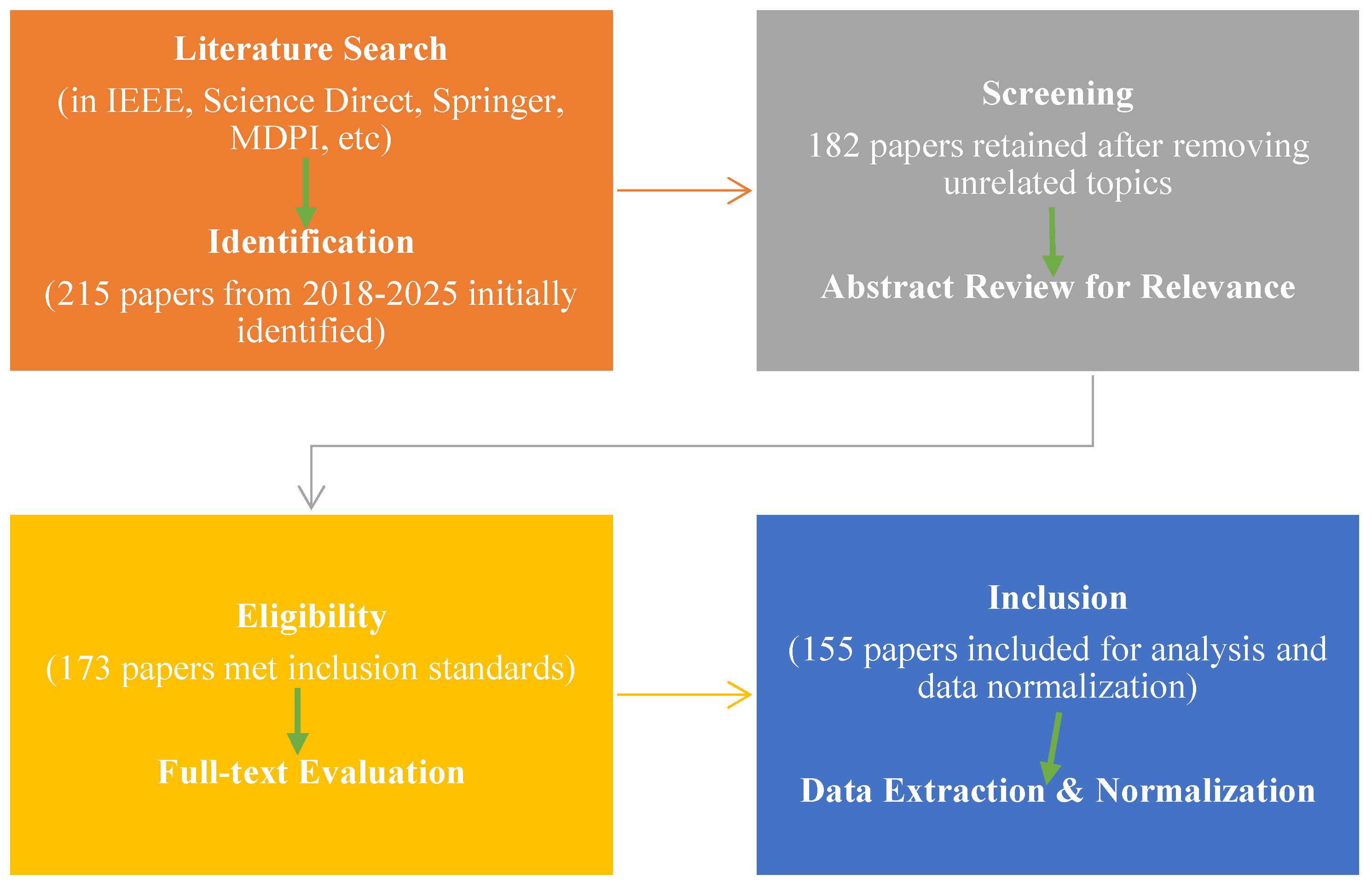
Figure 2.
Overview of 5G mmWave generations’ technology.
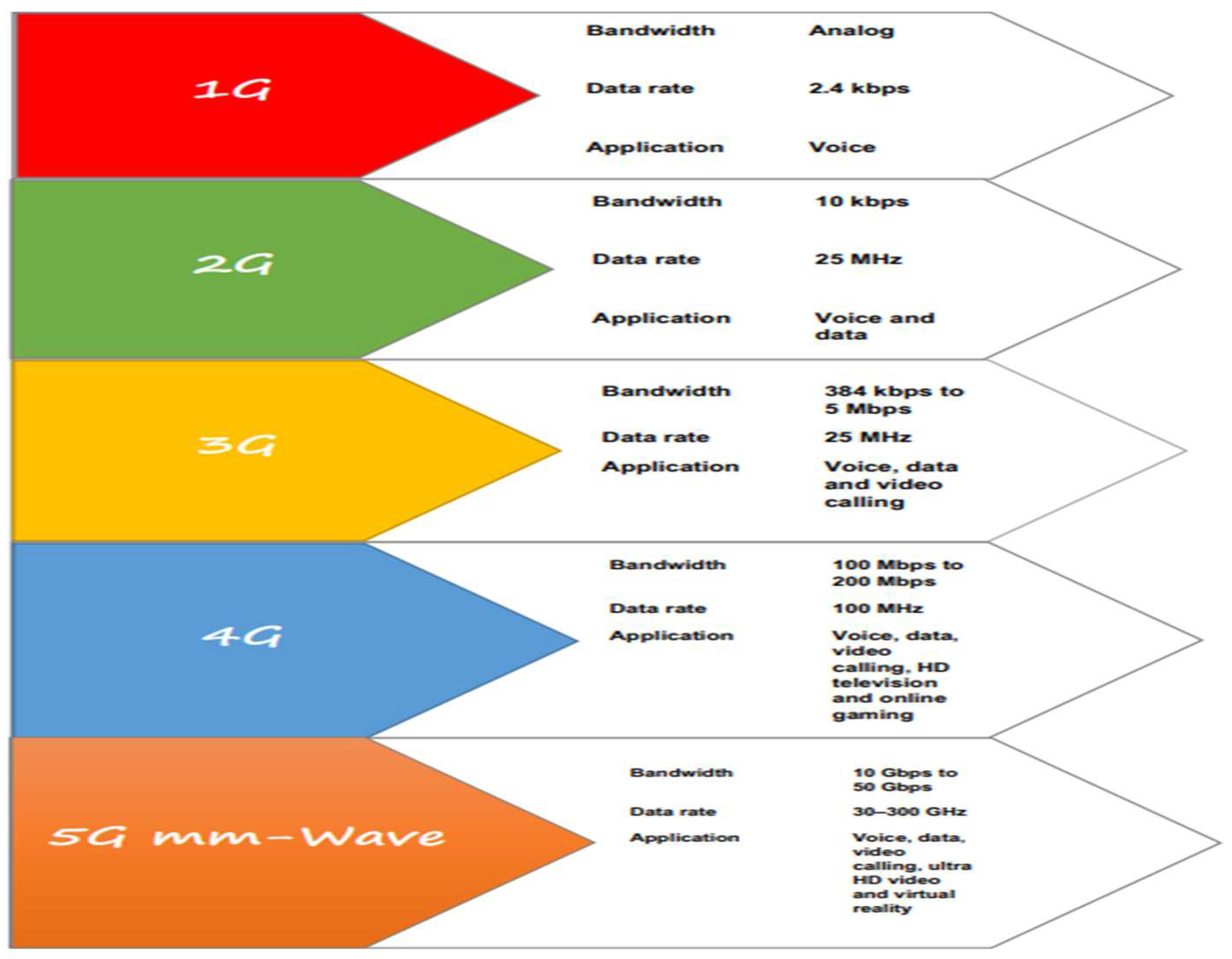
Figure 3.
Connectivity powered by 5G [3].
Figure 3.
Connectivity powered by 5G [3].
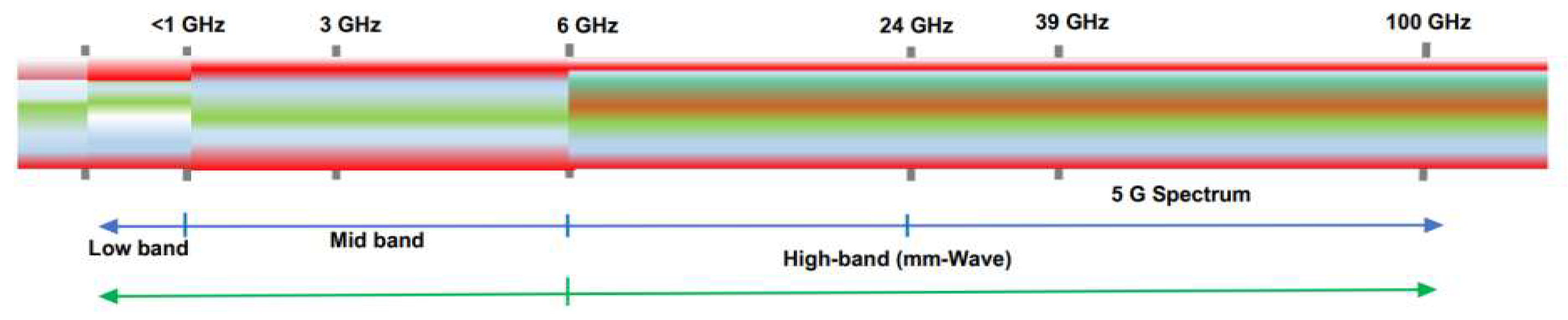
Figure 4.
Deployment areas of mmWave frequencies.
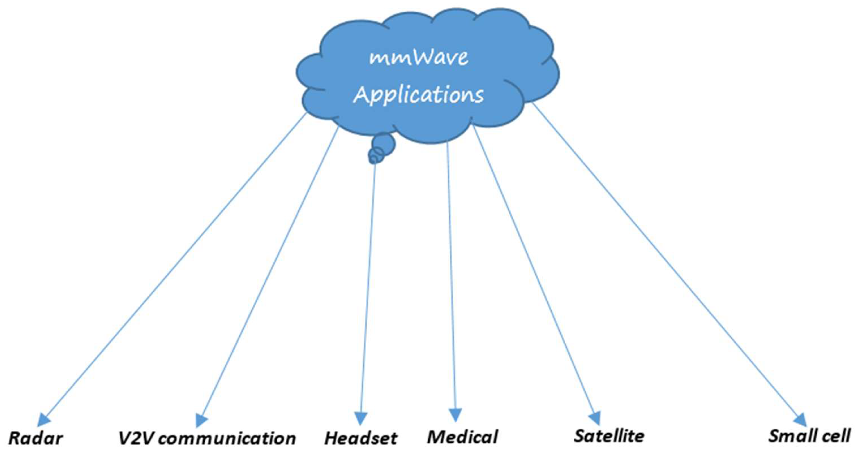
Figure 5.
Illustration of mmWave frequency [3].
Figure 5.
Illustration of mmWave frequency [3].
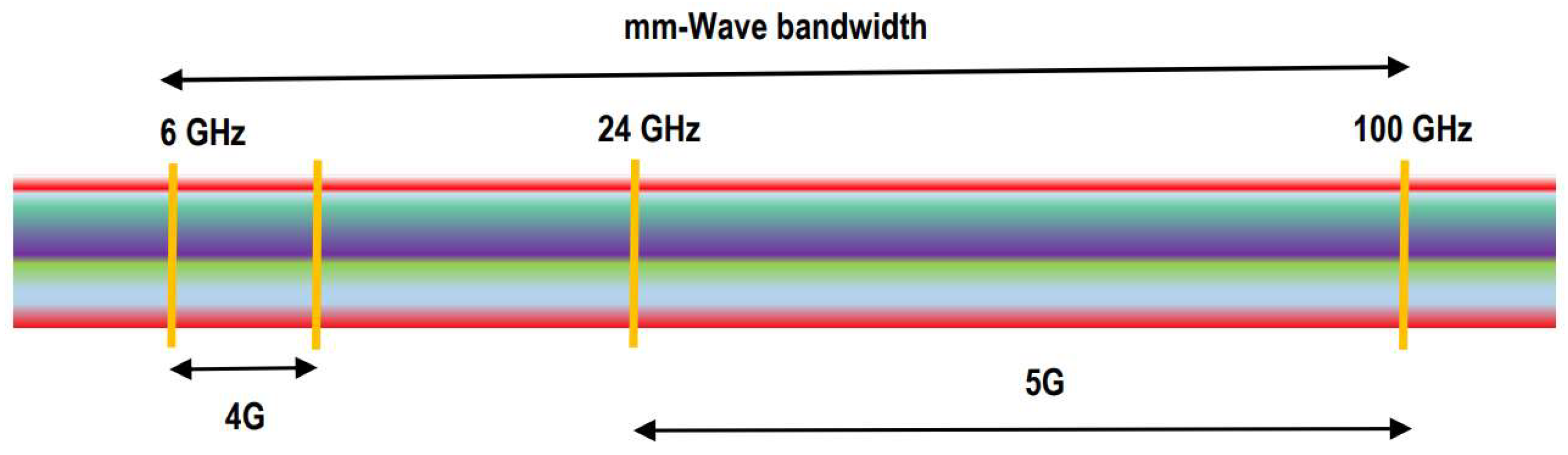
Figure 6.
The mmWaves advancements.
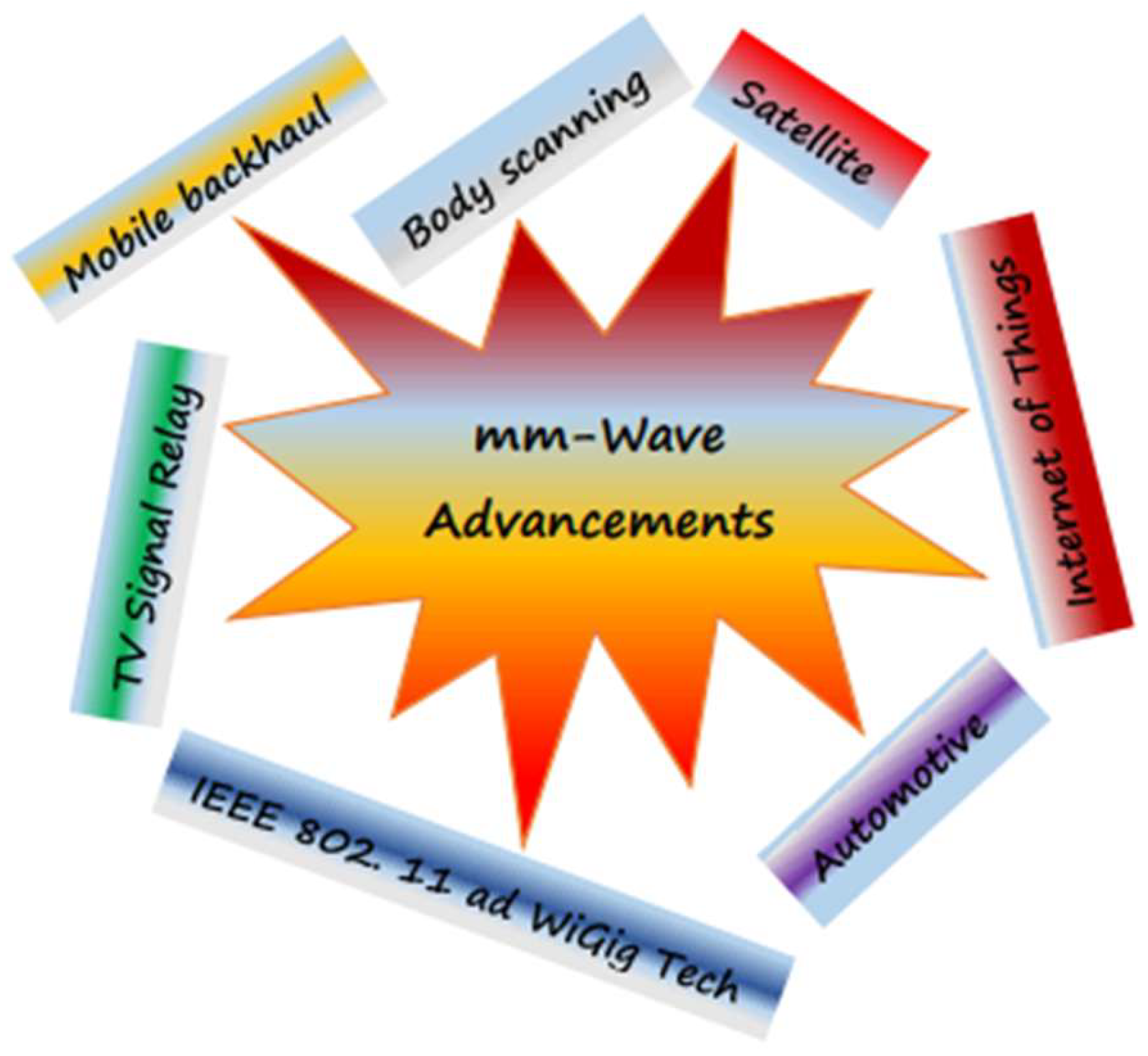
Figure 7.
(A) General layout of the proposed antenna design: (1) Single element, (2) Antenna array, and (3) proposed MIMO configuration [20]. (B) Radiation pattern measurements conducted in an anechoic chamber. (C) Reflection coefficient results. (D) Gain and efficiency at each design stage and (E) Reflection coefficient (S11) of the proposed MIMO antenna [20].
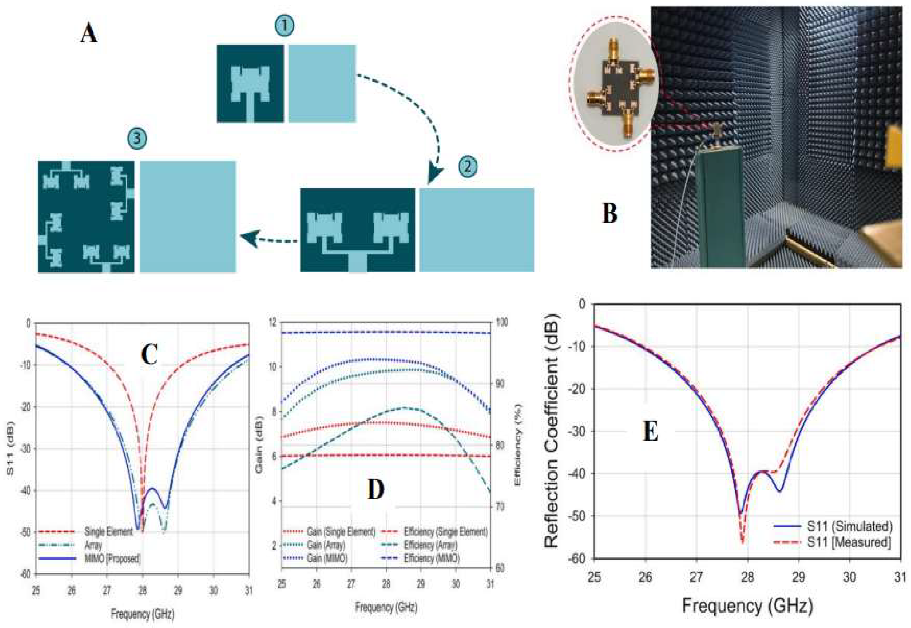
Figure 8.
(A) Fabricated smartphone antenna PCB showing (a) top view, (b) bottom view, and (c) the prototype connected to cables and loads. (B) Measurement setups for (a) S-parameters and (b) radiation patterns of the fabricated antenna element [21]. (C) Antenna elements efficiency results. (D) Measured S-parameters results of the proposed smartphone MIMO antenna [21].
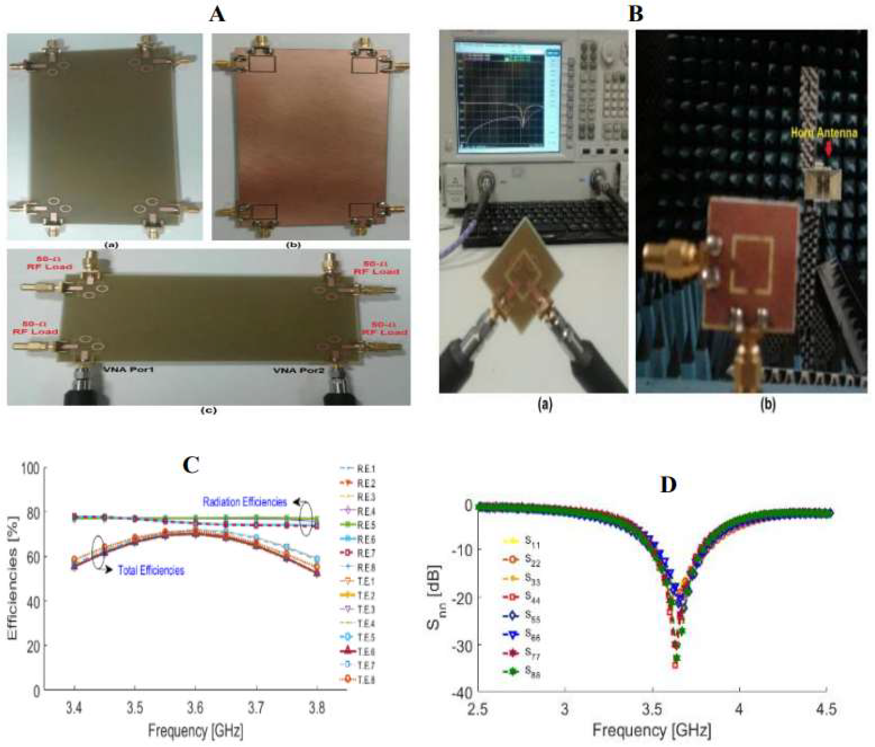
Figure 9.
Configuration of the proposed antenna array: (A) Front view and (B) Back view. Fabricated prototype of the array: (C) Front view and (D) Back view. (E) Comparison of simulated and measured return loss. (F) Key performance metrics of the proposed array [24].
Figure 9.
Configuration of the proposed antenna array: (A) Front view and (B) Back view. Fabricated prototype of the array: (C) Front view and (D) Back view. (E) Comparison of simulated and measured return loss. (F) Key performance metrics of the proposed array [24].
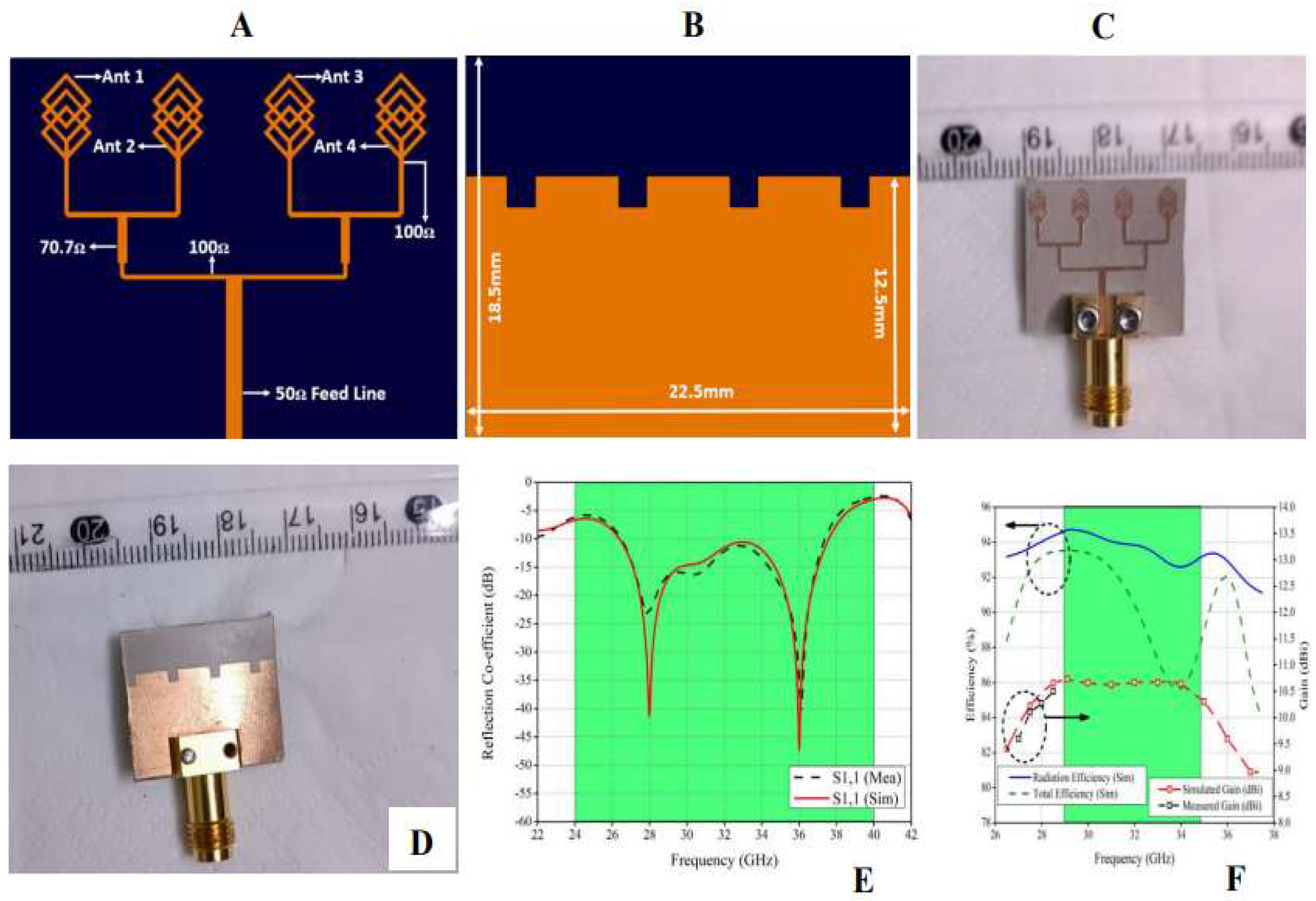
Figure 10.
Role of substrates in mmWave technology.
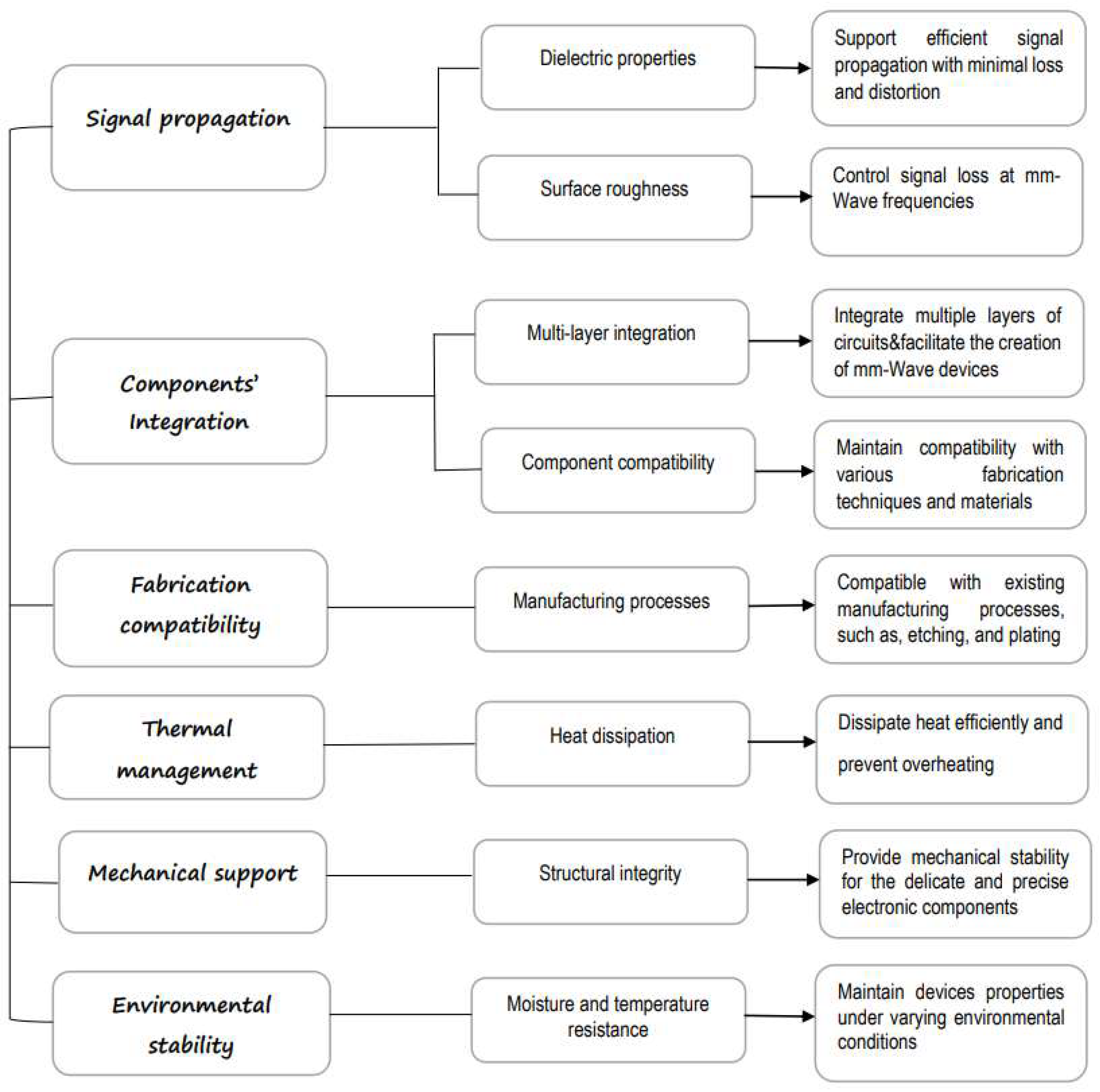
Figure 11.
Projected number of research papers per annum for “5G mmWave substrates” Source: Web of Science trends.
Figure 11.
Projected number of research papers per annum for “5G mmWave substrates” Source: Web of Science trends.
Figure 12.
Type of substrates used in mmWave communication.
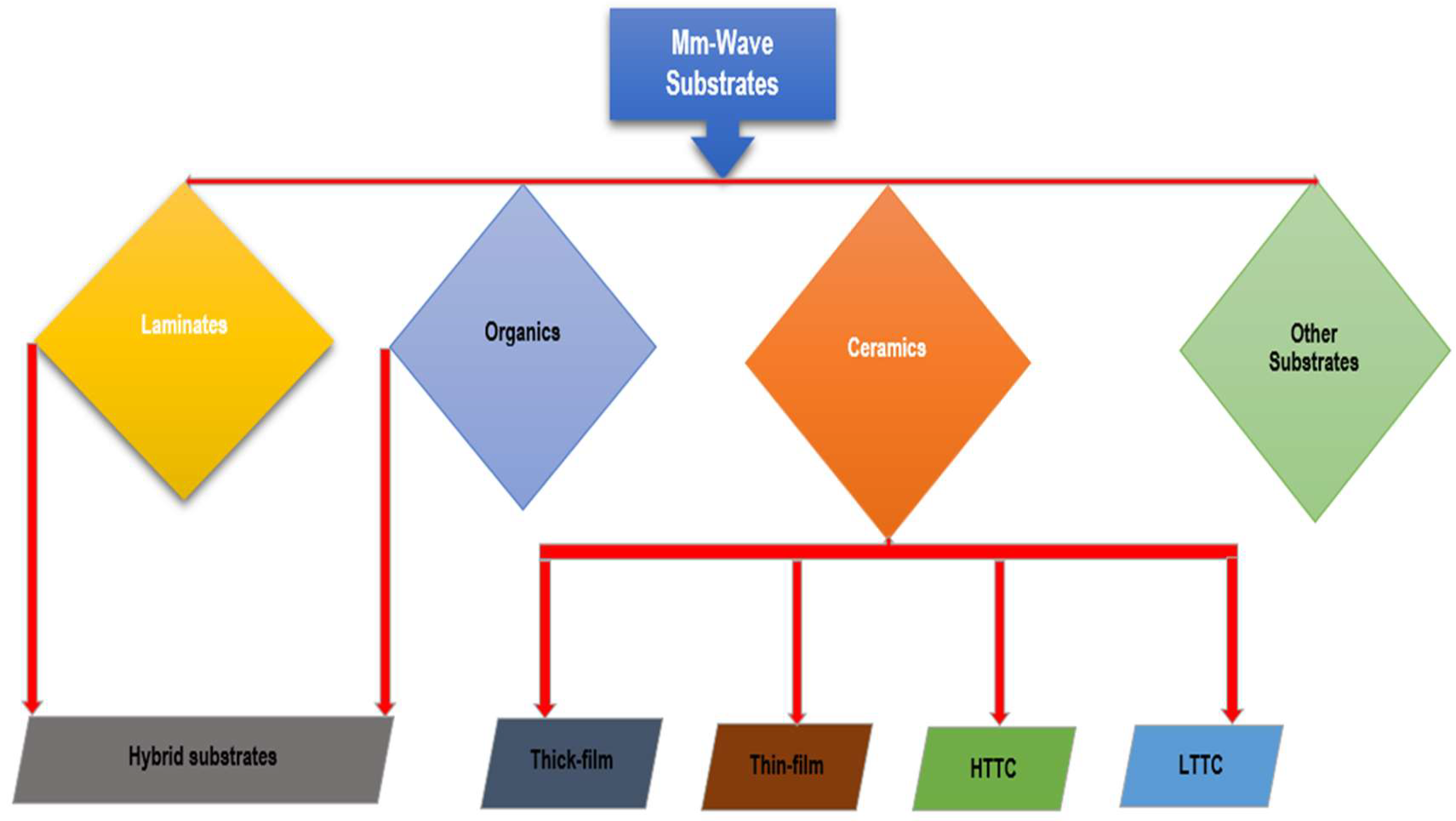
Figure 13.
Conductor loss against frequency for different copper foil roughness.
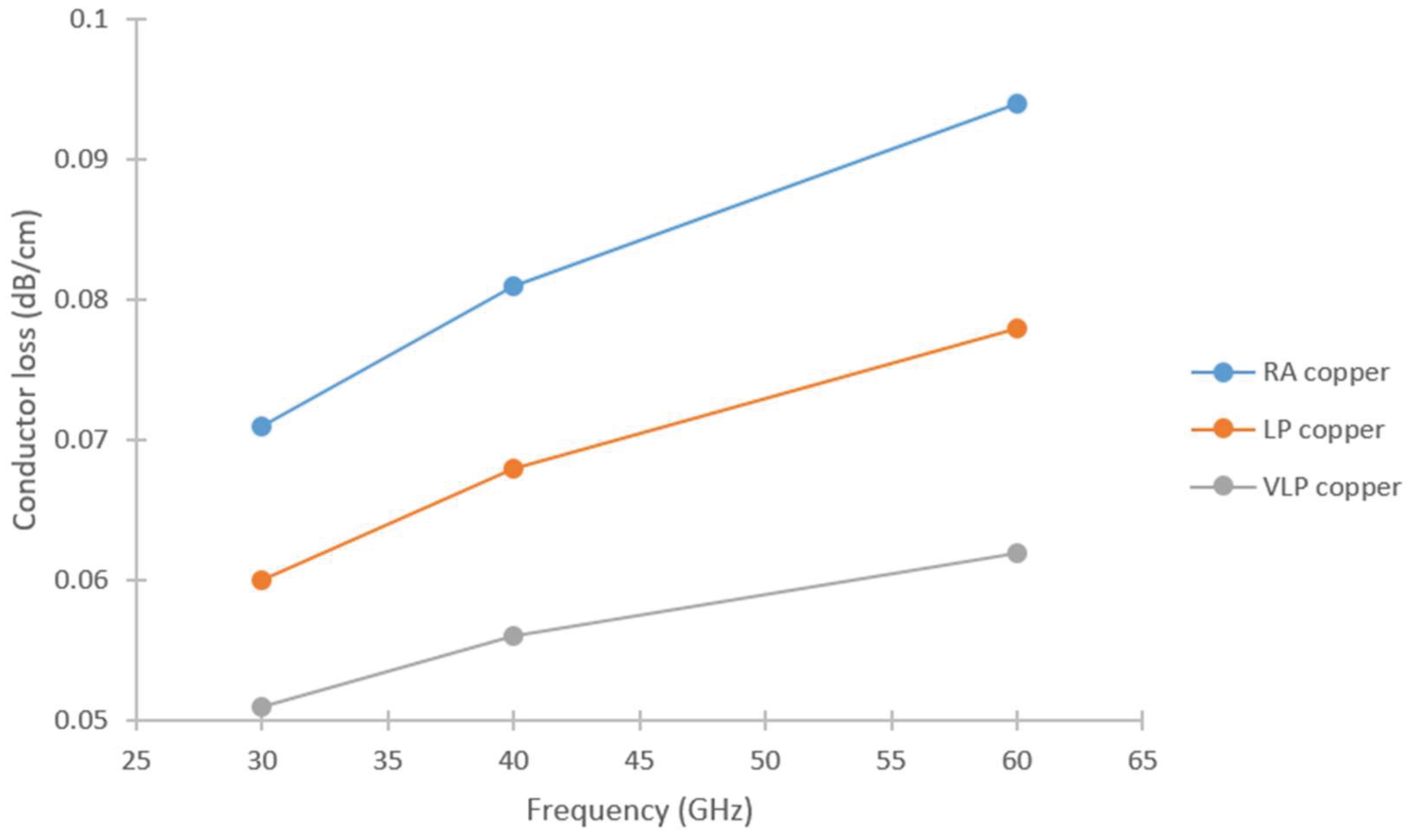

Table 1.
The mmWave frequency bands [11].
Table 1.
The mmWave frequency bands [11].
| Wave | Band | Frequency (GHz) | Wavelength (mm) |
|---|---|---|---|
| mmWave (30 – 300) GHz |
Q | 30 - 50 | 10 - 6 |
| U | 40 - 60 | 7.5 - 5 | |
| V | 50 - 75 | 06 - 4 | |
| E | 60 - 90 | 5 - 3.33 | |
| W | 75 - 110 | 4 - 2.72 | |
| F | 90 - 140 | 3.33 - 2.14 | |
| D | 110 - 170 | 2.72 - 1.76 | |
| G | 110 - 300 | 2.14 - 1 |
Table 2.
Comparative analysis of mmWave antenna advancement technologies.
| References | Designed Device | Relative Permittivity | Substrate Height (mm) |
Gain (dBi) |
Performance | Cost |
|---|---|---|---|---|---|---|
| [1] | Graphene liquid antenna | 2.55 | 1 | 7 | High gain, wide bandwidth for future 5G mmWave systems | Moderate |
| [16] | Dielectric resonator antenna | 2.2 | 0.787 | 5.45 | High efficiency and gain | Moderate |
| [20] | MIMO antenna integrated with ML based-gain prediction | 2.2 | 0.787 | 10.34 | Enhanced gain and bandwidth | High (ML integration) |
| [21] | 8-element slot antenna with dual-polarization | 4.4 | 1.6 | 3 | Good isolation and efficiency | Moderate |
| [23] | Two-layer metamaterial antenna | 2.2 | 0.78 | 11.27 | High gain, wide bandwidth | High |
| [24] | Wideband three-loop antenna array | 2.2 | 0.84 | 3.3 | High isolation and ECC performance | Moderate |
| [25] | Directional horn antenna | 4.4 | 3 | 8.06 | High directivity | Moderate |
| [28] | Antipodal Vivaldi antennas using RSIW | 4.4 | 0.8 | 1.41 | Improve the irradiation properties | Moderate |
| [29] | 50 μm polyimide layer based on-chip antenna using SIW | 3.5 | 0.1 | 1.5 | Applicable to use in THz integrated circuits | Simple design process, and cost effective |
| [30] | 8-element side-edge MIMO array | 4.4 | 0.8 | 3.9 | Enhanced isolation and gain | High |
| [31] | E-shaped H-slotted dual band mmWave MIMO antenna | 2.2 | 0.8 | 7.9 | Compact, good return loss | Low |
| [32] | Broadband dual-polarized MIMO antenna | 4.4 | 1.6 | 4.8 and 5.8 | High isolation, suitable for 5G | Moderate |
| [33] | 4-port MIMO antenna | 2.2 | 0.76 | 8.3 | Compact, low mutual coupling | Low |
| [34] | 3 –dB hybrid coupler (printed-RGW) | 2.94 | 0.762 | 3 | High isolation, compact | Moderate |
Table 3.
Summary and progress of 5G mmWave antenna developments.
| Reference | Substrates | mmWave Device | Frequency | Device Performance |
|---|---|---|---|---|
| [1] | Graphene | Beam-reconfigurable graphene liquid antenna | 28 GHz | Performs beam-steering up to 360° with 7 dBi of gain and a wideband of 10-dB impedance bandwidth of over 20% for 5G mmWave wireless communication systems |
| [20] | Graphene | 28 GHz MIMO Antenna for 5G applications | 28 | Enhanced due to tunable graphene conductivity |
| [46] | CLTE-MW | Microstrip line and filter structures | 60 | Stability maintained under high humidity; Low εr/tan δ improves frequency stability |
| [69] | FR-4 epoxy | Compact microstrip patch antenna | 40 GHz | Compact design, moderate gain and cost-effective |
| [70] | FR-4 | Compact multiband MIMO antenna system | Compatible with 5G/WLAN/WiFi-6 standards | Multiband, high diversity and compact design |
| [71] | FR-4 | C-slot microstrip patch antenna | 30 GHz | Good return loss, simple structure and low-cost material |
| [72] | BaF2 | mmWave antennas | mmWave range | High reliability, thermal stability and low loss |
| [73] | Graphene | Microstrip patch antenna | 29.6 - 40 GHz | The operating mode of the antenna achieved frequency reconfigurability |
| [74] | CLTE-MW | Dielectric terahertz characterization | sub-THz and THz | Revealed a more pronounced frequency-dispersive behavior among different materials |
| [75] | Arlon Diclad 880 | 5X20 massive MIMO antennas | 28.1 | Best suited for the development of an microstrip patch antenna array for the 5G wireless handheld communication devices |
| [76] | Arlon Diclad 527 | 2×2 MIMO antenna array | 28 | High isolation due to low-loss substrate and optimized spacing |
| [77] | Rogers RT5880 (lossy) | Elliptical slot circular patch antenna | Dual-band operation at 28 GHz and 38 GHz | Supports dual-band operation, optimized for 5G mobile applications with high isolation |
| [78] | Rogers RT/ Duroid-5880 | Rectangular microstrip patch antenna | 28 GHz | Low profile, high gain and suitable for compact devices |
| [79] | FR-4 | Wideband MIMO antenna with symmetry | mmWave band | Polarization diversity and compact design |
| [80] | FR-4 | Two-monopole MIMO with parasitic elements | Sub-6 GHz | High isolation and improved MIMO performance |
| [81] | FR-4 | Super-wideband MIMO antenna | 2.3-23 GHz | High isolation and optimized bandwidth |
| [82] | FR-4 | 4-Port octagonal MIMO antenna | 3.5-11 GHz | Low mutual coupling and broadband |
| [83] | Rogers RT/Duroid 5880 | Dual band high gain MIMO antenna | 28/37 GHz | High gain and compact 4-port design |
| [84] | FR-4 | UWB MIMO with X-shaped stubs | 1.9–14 GHz | High isolation and good bandwidth |
| [85] | Rogers-RO4350B | High Gain Array MIMO antenna | 28 GHz | High gain, array performance, for mmWave |
Table 4.
Overview of fabrication techniques: Benefits, limitations and costs implications.
| Technique | Advantages | Disadvantages | Cost |
|---|---|---|---|
| Coating | Simple and flexible to various materials | Limited thickness control | Low |
| Sputtering | Precise control of thickness and composition | High vacuum needed and slower deposition rate | Medium to High |
| Photolithography | High resolution and precise designing | Not suitable for flexible substrates | High |
| 3D Printing | Fast prototyping and customizable geometries | Material restrictions and surface roughness issues | Medium |
| Fabrication with Molds | Repeatable shapes and suitable for flexible substrates | Limited accuracy, wear and tear of molds over time | Low to Medium |
| Hot Pressing | Strong bonding and appropriate to multilayer structures | Needs heat-sensitive materials and irregular pressure may affect uniformity | Medium |
| SIW | Compact and easy integration with PCBs | Limited bandwidth and design difficulty | Medium |
| TGV | Excellent RF performance | Costly process and difficult orientation | High |
| FD-SOI | Low power consumption | Less mature ecosystem than bulk CMOS | Very High |
Table 5.
Summarized features of involved studies.
| Reference | Substrate Materials | Thermal Conductivity |
Temperature Range |
Temperature Dependence |
Cooling Approach |
|---|---|---|---|---|---|
| [62] | FR-4&hybrid | Not mentioned | -55 0C to +150 0C | Not mentioned | Passive (material selection) |
| [111] | CVD diamond | Not mentioned | Not mentioned | Not mentioned | Passive (substrate selection) |
| [112] | AIN:Mo | Not mentioned | Up to 1000 0C | Yes | Passive (material selection) |
| [113] | SiC with SiO2 | Not mentioned | 54.3 0C to 29.1 0C | Yes | Passive (material selection) |
| [114] | c-BN&Si | c-BN>Si | Reduce from 5-17 0C | Yes | Passive (substrate selection) |
| [115] | AIN&GaAs | AIN>GaAs | 93-95 K (op.), 80 K (heat) | Not mentioned | Passive (substrate selection) |
Table 6.
Methods for improving thermal performance.
| S/N | Heat Dissipation Issues | Methods | Procedures |
|---|---|---|---|
| 1. | Thermal stress | Component spacing | Providing adequate spacing between components helps prevent heat concentration and reduces the risk of thermal stress |
| Thermal relief structures | Implementing thermal relief structures in copper planes or pads reduces the thermal expansion mismatch between components and the metal substrate, mitigating thermal stress | ||
| 2. | Solder mask and surface finish | Solder mask material | Selecting a solder mask material with good thermal resistance properties helps withstand high operating temperatures and prevents delamination or cracking |
| Surface finish | Opting for a surface finish that provides reliable solder joint formation and excellent thermal conductivity, such as ENIG (Electroless Nickel Immersion Gold), promotes robust thermal performance | ||
| 3. | Warping and distortion | Metal core thickness | Choosing an appropriate metal core thickness that balances mechanical stability and heat dissipation can help minimize warping issues |
| Thermal expansion management | Understanding the CTE of the metal substrate and other PCB materials and ensuring compatibility can prevents warping and improves thermal stability | ||
| 4. | Mechanical support and mounting techniques | Mounting holes | Incorporating sufficient mounting holes and using appropriate hardware, such as screws or standoffs, provides mechanical stability and prevents excessive stress on the PCB |
| Shock and vibration resistance | Designing the PCB layout and selecting mounting techniques that offer resistance to shock and vibration ensures reliable operation in harsh environments |
Table 7.
Summary of techniques to minimize signal transmission losses in mmWave substrates.
| Reference | Substrate Type | Technique Used | Frequency Range | Achieved Reduction Loss |
|---|---|---|---|---|
| [125] | CLAF-SIW | Cavity-stacked filter design | mmWave | Enhanced filter performance with reduced insertion loss |
| [126] | GaAs-based TFIPD | Bandpass filters design | 3.3-5.0 GHz | Insertion loss reduced to 0.755-1.237 dB |
| [127] | Multi-layer SiCOx/SiOx coating | Corrosion-resistant coatings | Not specified | Improved signal integrity |
| [128] | Epoxy with aluminium flakes | Stearic acid and Al2O3 coated Aluminium flakes | 1-10 GHz | Dielectric loss reduced from 0.037 to 0.005 |
| [129] | FCCL on polyimide | Direct metallization | 0.1-40 GHz | Insertion loss of (0.03, 0.04 & 0.06) dB/mm at (20, 28 & 40) GHz, respectively |
| [130] | Graphene | Circularly polarized 1×2 array antenna | 2.345-2.555 THz | Achieved 99.8% radiation efficiency |
Table 8.
Representative RMS roughness and estimated loss impact.
| Frequency (GHz) | Skin depth δ (µm) | (Fr) (RA, Δ=1.8 µm) | (Fr) (VLP, Δ=0.4 µm) | % reduction in conductor loss (RA→VLP) |
|---|---|---|---|---|
| 30 | 0.382 | 1.904 | 1.619 | 15.0% |
| 40 | 0.330 | 1.917 | 1.661 | 13.4% |
| 60 | 0.270 | 1.932 | 1.714 | 11.3% |
Table 9.
Computed conductor loss cm-1.
| Frequency (GHz) | RA Copper (1.8 µm) | LP Copper (0.9 µm) | VLP Copper(0.4 µm) | Loss Reduction (RA→VLP) |
|---|---|---|---|---|
| 30 | 0.071 dB/cm | 0.060 dB/cm | 0.051 dB/cm | 28% |
| 40 | 0.081 dB/cm | 0.068 dB/cm | 0.056 dB/cm | 31% |
| 60 | 0.094 dB/cm | 0.078 dB/cm | 0.062 dB/cm | 34% |
Table 10.
Comparative analysis of mechanical properties of mmWave substrate materials.
| Reference | Material/Substrate | Mechanical Characteristics | Methods Applied | Key Findings |
|---|---|---|---|---|
| [136] | PI & PET with Ag Nanowire Electrodes | High flexibility; Elastic modulus PI ~5.27 GPa, PET ~3.31 GPa | Bending cycles up to 400,000 | Minimal resistance increase; excellent strain accommodation |
| [137] | Ferrite-based nanoparticles on flexible substrate | Enhanced structural/electrical integrity under stress | Structural, optical, electrical characterization | Ferrite inclusion potentially supports improved mechanical endurance |
| [138] | Al–Si–Cu/Al–Cu hybrid structures | Microstructure evolution with thickness; improved grain structure | Electron beam DED; hardness tests | Substrate thickness critical to mechanical robustness |
| [139] | SiNx on SiO2 | Simulated high mechanical stability and adhesion | Molecular dynamics simulations | Potential use in high-performance, mechanically stable environments |
| [140] | 2D materials on soft substrates | Measured Young’s modulus, fracture strain, stress behavior | AFM, tensile and nanoindentation tests | Reveals mechanical limits of 2D-on-soft system |
| [141] | Gradient nanocomposite on soft substrate | Enhanced surface hardness and adhesion | Nanoindentation, SEM | Gradient coatings improve mechanical resilience |
| [142] | Ag–Mn doped ZnO on glass | Structural change due to heating; mechanical property alteration | XRD, SEM, nanoindentation | Thermal treatment modulates mechanical properties |
| [143] | Hybrid chitosan-silica on Al | Improved toughness and flexibility | Mechanical and chemical testing | Biocomposite coatings enhance durability |
| [144] | Multilayer TiN | Failure mechanisms under mechanical stress analyzed | Micro/nano-mechanical analysis | Interfacial mechanics critical for durability |
| [145] | Cu-alloy on Al | Hardness and strength dependent on microstructure | Laser deposition& microhardness testing | Laser parameters critically influence mechanical behavior |
Table 11.
Summary of hybrid materials for mmWave substrates.
| Reference | Substrate Materials | Frequency Band | Possible Applications |
|---|---|---|---|
| [46] | Thermosetting siloxane hybrid | Not explicitly mentioned | Advanced electronic packaging |
| [137] | Ferrite-based nanoparticles | Not specified | Chemical sensing |
| [147] | Low-loss material (PTFE or similar) | mmWave and THz | mmWave/THz communication systems |
| [148] | Alumina ribbon ceramic | 24-100 GHz (mmWave) | 5G and mmWave communication |
| [149] | Thin alumina | mmWave | Microstrip leaky wave antenna |
| [150] | Silicon-based for MEMS | THz | MEMS switch design |
| [151] | Graphene-based | 5G (Wideband) | For 5G mobile communication |
| [152] | Lithium niobate (LiNbO3) | 50.74 GHz | For mmWave front-end filters |
| [153] | Rogers RT5880 and RT5870 | 5.2 GHz | For sub-6 GHz 5G applications |
| [154] | Alumina ribbon ceramic | mmWave | High-performance filters for 5G small cells |
Disclaimer/Publisher’s Note: The statements, opinions and data contained in all publications are solely those of the individual author(s) and contributor(s) and not of MDPI and/or the editor(s). MDPI and/or the editor(s) disclaim responsibility for any injury to people or property resulting from any ideas, methods, instructions or products referred to in the content. |
© 2026 by the authors. Licensee MDPI, Basel, Switzerland. This article is an open access article distributed under the terms and conditions of the Creative Commons Attribution (CC BY) license (http://creativecommons.org/licenses/by/4.0/).
Copyright: This open access article is published under a Creative Commons CC BY 4.0 license, which permit the free download, distribution, and reuse, provided that the author and preprint are cited in any reuse.


