
Submitted:
31 May 2025
Posted:
03 June 2025
You are already at the latest version
Abstract
In the Internet of Things (IoT) era, the demand for cost-effective, flexible, wearable antenna and circuits has become very high. Accordingly, screen printing techniques are becoming more popular due to their lower costs and high-volume manufacturing abilities. This paper presents and investigates a full-screen printed 1 x 4 Quasi-Yagi-Uda antenna array on a high-transparency flexible Zeonor thin-film substrate for emerging 26 GHz band 5G applications. As part of this study, screen printing implementation rules are developed by properly managing ink layer thickness on a transparent flexible Zeonor thin-film dielectric to achieve a decent antenna array performance. In addition, a screen-printing repeatability study has been carried out through a performance comparison of 24 antenna array samples manufactured by our research partner from CEA-Liten Grenoble. Despite the challenging antenna array screen-printing at higher frequencies, the measured results show a good antenna performance as anticipated from the traditional subtractive printed circuit board (PCB) manufacturing process using standard substrates. It shows a wideband matched input impedance from 22-28 GHz and a maximum realized gain of 12.8 dB at 27 GHz.
Keywords:
antenna design
; Yagi-Uda antennas
; screen-printed antennas
; antenna arrays
; 5G
; flexible antennas
1. Introduction
The growing applications of the Internet of Things (IoT) and 5G/6G have raised the demand for flexible, wearable, low-cost, and mass-manufacturing microwave and millimeter-wave components. These applications involve billions of connected devices performing several operations such as sensing, data acquisition, processing, and transportation [1,2,3,4]. Modern printed electronic circuits need to be low-cost and mechanically flexible for wearable applications to fulfill the requirements of mass production and ease assembly conditions on different surfaces. Unfortunately, traditional electronic manufacturing techniques such as subtractive fabrication technologies are not technically and economically competitive in mass production [5,6]. They are expensive, resulting in material waste, and are not ideal for mass manufacturing [7]. Recently, various printing techniques have been adapted for electronics manufacturing. For instance, gravure printing, flexography, inkjet printing, and more specifically screen printing [8,9,10,11]. The latter seems to be a promising and cost-effective technique for printable microwave/millimeter-wave/THz circuits such as RFID tags, RFIC packaging, energy-harvesting rectennas, and wireless communication antennas [11,12,13]. Today, screen printing offers repeatable accurate printing of antenna circuits on inexpensive flexible thin-film materials such as glass, laminates, and plastic, providing a large substrate selection for flexible electronics [10]. Nevertheless, specific arrangement and parameters such as ink, printing, and screen conditions must be carefully monitored at higher frequencies on highly flexible transparent substrates. Moreover, depending on ink composition and ink/substrate interaction, post-processing through heat treatment at 135° might be required [11].
Given what has been achieved in the screen-printing research area, high-frequency circuits involving the screen-printing process on transparent thin-film substrates are still missing from the literature. Moreover, the implementation challenges associated with those types of substrate materials have not been previously revealed. For these reasons, we believe that clarifying screen-printing issues on highly transparent substrates at higher frequencies will provide practical performance optimization guidelines to microwave/millimeter-wave circuits and antenna designers. As a proof of concept, a full-screen printed 1 x 4 Quasi-Yagi-Uda antenna array on a high-transparency flexible Zeonor thin-film substrate is presented and analyzed for emerging 26 GHz band 5G applications. Thanks to the suggested screen-printing improvement, the implementation of the 1 x 4 Quasi-Yagi-Uda antenna array prototype has been highly optimized. Moreover, a repeatability test has been performed by manufacturing 24 antenna array samples equally distributed over 4 substrate sheets for performance comparison. The achieved comparison performances show a good concordance over the considered frequency range from 20 GHz to 30 GHz. They exhibit a large bandwidth and high gain as expected from the traditional subtractive printed circuit board (PCB) manufacturing process using standard substrates.
2. Screen-printing technique
Figure 1 shows a screen-printing process description. Ink is spread on a stencil by a squeegee. Thus, when the stencil is transparent, the ink is deposited on the substrate. The process requires a precise management of stencil mesh and squeegee properties, as well as production techniques. It may also require tightly controlled parameters during printing. Furthermore, ink transfer is mainly influenced by the screen mesh, squeegee speed, and pressure on the screen. The thickness and accuracy of the printed layer are affected by the ink’s rheological properties. It should be noted that thicker ink deposition involves lower resolution [14].
The parameter selection involves some rules consideration for antenna design, including minimum line width, spacing between adjacent lines, and feeding techniques. The screen printing prototyping uses a commercial screen printing machine. However, to improve cost-effectiveness, only textile stencils were utilized to print all the designed antennas. The substrate is the first element to be selected appropriately, especially at the millimeter-wave frequency range, where it plays a key role in antenna performance. In the millimeter wave frequency range, the substrate plays a key role in antenna performance. It must have low-loss characteristics and be compatible with the physicochemical properties of the selected ink. For our screen printing process, a Zeonor [15] substrate with a thickness of () has been chosen. In order to ensure a proper printing and good adherence of ink with the substrate it must have an oxygen free plasma treatment. Substrate selection is a key factor in ensuring good compatibility with inks, particularly with reagrd to the substrate’s physical and chemical properties. In this section, we expose the essential properties that promote this compatibility. For instance, in the case of inkjet or screen printing with metallic inks, such as silver ink, the substrate must have a microporous receiving layer, either by plasma etching to create nanometric roughness, or by depositing a porous low dielectric such as a fluoropolymer or polystyrene, which enables better adhesion and avoids excessive ink diffusion. The characteristics of silver inkjet printing were intensively investigated with control of surface energy, which is why the choice of substrate can greatly affect the quality of the print and consequently the electrical performance of the deposited silver layer. In this study, the Kapton was treated with an oxygen-free plansma to create the micro-pored layer without degradation of the electrical properties of the zeonor [16].
To minimize losses in metallic parts of the antenna, ink selection is a key point in our study. The selected ink must be sufficient for screen-printing and have high conductivity with relatively low cost. Thus a trade off between cost and conductivity should be found. As initial value, the thickness of ink is fixed to two penetration depth (). Taking into account those constraints, the ECI011 nano-particles silver ink from Henkel has been selected with a conductivity of . According to equation 1, the penetration depth can be computed at and the needed ink thickness deduced. Table 1 summarize the properties of this ink.
With such ink thickness, the expected resolution should be around for ink strips and for slots formed on ink strips. This resolution should be suitable for printing antennas in the 5G ETSI millimeter-waves frequency range. As the substrate and the ink properties are set, a feeding method is essential. Various feeding solutions on flexible substrates can be employed for this purpose. For a comprehensive characterization of the manufactured antenna prototypes, a 50 microstrip line along with a Southwest Microwave End launch connector are implemented. The designed micro-strip lines consist of a signal strip printed on the top face of the substrate, and a ground plane printed on the bottom face. To assess the thickness of selected ink layer , the lineic attenuation of a 50 micro-strip line is extracted from full-wave simulations. The results plotted in Figure 2 shows that increases the thickness of printed layers up to allows to reduce metallic losses. Indeed, increasing the thickness does not significantly reduce metallic losses and does not improve the resolution of the printed patterns. [14].
3. Quasi-Yagi-Uda antenna elements
3.1. Design optimization
The single-element Quasi-Yagi-Uda antenna configuration is shown in Figure 3.
Its geometrical Parameters have been optimized according to the design rules described in [17,18,19,20]. The initial Quasi-Yagi-Uda antenna configuration is designed using a full ground plane as shown in Figure 3 (a). Typically, a Quasi-Yagi-Uda antennas antenna consists of two driven elements fed by a microstrip line and several directors (parasitic elements), as shown in Figure 3. For design optimization, 3D HFSS electromagnetic (EM) simulation software has been used while considering the southwest end-launch connector effect. It was demonstrated from simulation results that the distance between the ground plane and driven element (d’) impact significantly matching bandwidth, however, the distance between different directors (d) mainly impacts the gain. The length sets the antenna operating frequency, whereas and set the antenna’s lower and higher cut-off frequencies. Several director configurations have been tested. A trade-off between directivity, directors’ losses and the overall antenna size has enabled us to limit the directors number to 4 directors placed on the top layer. It was reported that a double row of four directors placed respectively on the top and bottom layers may increase the antenna gain [20].
In the context of our study, the expected gain has not been achieved due to high metallic losses and the thickness of the selected substrate. The computed values from [14] have been modified by a scale factor while considering the dielectric constant parameter. Then, the antenna dimensions were optimized to achieve good impedance matching and the flattest realized gain over the 24.5 GHz to 27.5 GHz frequency band. For instance, simulation results show that an optimized 4 directors configuration exhibits a realized gain of 9.8 dB (11.1 dB in an 8 directors configuration). This represents an increase in antenna size from to (about a 75% size increase) and a radiation efficiency variation from 65% (8 directors) to 69.5% (4 directors).
Now, we optimize the ground plane to reduce the ink consumption while increasing the flatness band of the gain and improving the side lobe rejection. The proposed ground plane configuration is shown in Figure 3 (b). and , have been optimized through a rigorous parametric study. Several effects can be observed on the variation of the gain versus frequency as shown in Figure 4a and Figure 5a. However, simulation results demonstrate that If the is too short, the resulting ground does not affect antenna performance. An optimum value of has been set to in the proposed antenna configuration, nevertheless, higher length causes a reduction in antenna bandwidth (see Figure 4b). Regarding the impact of variations, the parametric study results are plotted in Figure 5a. It shows that the optimum value is approximately equal to the length of a reflector given in [18]. For lower values of , the edge of the ground plane does not act as a reflector and higher values than optimal decrease the bandwidth and the maximal gain. Careful attention to input impedance matching (Figure 4b and Figure 5) shows that those parameters can optimize the antenna’s bandwidth. Setting the proper values of and enables the flattest peak gain in the desired bandwidth.
A further effect concerning the out-of-band gain reduction is also observed. As can be seen, the gain at 20 GHz has been reduced by more than 8 dB (from 1.2 dB to -7.5 dB). Under the same design modifications, the in-band gain variation is reduced to less than 0.5 dB (from 1.3 dB to 0.3 dB). Table 2 summarizes the optimized geometrical parameters of the antenna including, the 4 directors configuration and modified ground plane.
Figure 5 shows the simulation results of the optimized Quasi-Yagi-Uda antenna. Those results show a maximum gain of 9.8 dB at 27 GHz with a variation of only 0.3 dB within the considered frequency band. In conclusion, the proposed technique allows ground plane reduction from to , representing a decrease of 61%.
As regards the radiation pattern performance shown in Figure 7, the newly optimized antenna parameters have only an influence on the H-plane radiation pattern with no major changes on the E-plane. In the proposed antenna configuration side lobes at can be reduced from -6 dB to -12.5 dB.
3.2. Measurements
This section deals with the experimental characterization of the single Qausi-Yagi-Uda antenna. For that purposes, 24 antenna prototypes, printed on 4 different sheets, have been printed by CEA-Liten "Ares" facilities. Measurements for performances investigation have been performed in the im2np lab. The size of the printed antenna and the end-launch connector compared to a 50-cent coin is given in Figure 8.
Measurements have been performed using a DRH 67 GHz RF-SPIN antenna and a MS4647B 4 ports 70 kHz-70 GHz Anritzu VNA. The free space test bench used allows to perform radiation pattern measurements in E and H planes, realized gain in a given direction and matching as function of the frequency up to .
The measurement results are plotted in Figure 9 and in Figure 10. For each sheet of printed antennas, the mean (see Figure 9a) and standard deviation have been computed from individual measurement of the realized gain. Standard deviation for each sheet plotted in Figure 9b gives further information on the repeatability of the screen printing process. The standard deviation is lower than over the to frequency band. It involves a very low dispersion for 24 measured antennas. The maximum measured gain is in the line of sight direction. A small shift of approximately , (less than ) can be observed on measurements. Geometrical measurements of the printed antennas and retro-simulations does not allow to affirm that geometrical issues introduced during the printing cause this mismatch. Retro-simulation of the antenna with instead of allows to explain this slight frequency shift between simulations and measurements (see Figure 9a). By adopting the same approach measurements results are plotted in Figure 10. The same discrepancy between simulations and measurements can be observed and same reasons can be invoked to explain the observed frequency shift. Higher dispersion on this parameter can also be observed. Still, in this case, a little frequency shit between measurements of different antennas causes higher variations of the than for gain versus frequency values. The measured matching bandwidth ranges from .
Radiation pattern in E and H planes have been measured at , , ,. and . The results of the simulated and measured normalized gain are plotted in Figure 11. As can be seen, a good agreement between measurements and simulations is achieved. For H-plane at all measured frequencies, side lobes are below and front to back ratio is lower than . For E-plane the side lobe level are bellow except at . Measurement shows a maximum beamwidth of in H-plane and in E-plane.
Comparison with other published Quasi-Yagi-Uda antennas realized with standard technologies shows that similar performances can be achieved by a careful optimization of screen-printing process and the design (see Table 3).
4. Quasi-Yagi-Uda antenna array
4.1. Design methode
A corporate feed network using three rounded shapes Wilkinson dividers is adopted for the 1 x 4 Quasi-Yagi-Uda antenna array design. The selected feed network configuration allows more control of feeding each antenna element (amplitude and phase); hence, they are ideal for several antenna array applications such as multi-beam arrays, scanning phased arrays, or shaped-beam arrays [18]. Typically, two power divider types may be used for the power distribution in the antenna arrays, reactive T-junctions and Wilkinson power dividers. The T-junctions are lossless and simpler to design but do not provide isolation between the output ports. The Wilkinson dividers involve higher design and fabrication complexities, and they are not entirely lossless since reflected power is dissipated in the resistor. However, they provide isolation between output ports, which prevents mismatches and reflected signals from propagating to other parts of the array. To reduce the undesirable coupling and improve isolation between the Wilkinson output ports at higher frequencies, two microstrip lines have been added between the two output ports [25]. It should be noted that the isolation resistor between the output ports (ports 2 and 3) has been implemented using a per square thin layer carbon past.
The designed Wilkinson power divider and its simulated S-parameters are shown in Figure 12a and Figure 12b, respectively. The simulation results show a maximum insertion loss of and isolation between the output ports (ports 2 and 3) better than in the frequency range from to .
EM simulations have also been performed of the array without the feeding network to evaluate mutual coupling between antenna elements which impact the total array performance. The optimum distance necessary to avoid grating lobes is set to in the proposed array design. The arrangement adopted could add to the achieved gain to reach in the main direction of radiation. The obtained Results show that the added gain is much lower and that the matching is modified (see Figure 13). The study of the current distribution and transfer parameters between adjacent antennas () (see Figure 13) shows that the proximity of antennas most likely causes this reduction. This generates coupling between the radiating elements and reduces the antenna array gain.
The undesired grating lobes are usually controlled by constraining the distance between antenna elements.
Given our printing resolution limitation, we further spaced the antenna elements to improve the gain, even if doing so results in a possible side lobes generation [18]. Under those considerations, a maximum of side lobe rejection level and a gain as close as possible to the theoretical limit of may be exhibited. Then, spacing between array elements of is required to satisfy our criteria (see Figure 13).
The overall dimension of the designed 1 x 4 Quasi-Yagi-Uda antenna array is around by , as shown in Figure 14a. Figure 14b shows input impedance matching and gain simulation results including End Launch connector effect, over the frequency range of to . As can be seen, a maximum gain of in the main radiation direction is achieved. The antenna array maintains a good input impedance matching over the to frequency range. As expected, the minimum side lobe rejection level is The simulated radiation efficiency spans from 50 to 55 % in the frequency range of interest.
4.2. Measurements
For comprehensive characterization, 24 antenna arrays have been prototyped over 4 sheets by the CEA-LITEN laboratory. Figure 15 shows the real size of an antenna array with its connector beside a 50-cent coin. 24 antenna arrays have been printed by the CEA and equally distributed over 4 sheets.
The gain in the main direction of radiation and the matching of each array has been measured with the same test bench as for single Quasi-Yagi-Uda antenna elements. The results plotted in Figure 16a and Figure 16b show the mean of measured gain and it’s standard deviation for each of the 4 sheets. The measurements results compared with simulations show a good agreement for the four printed sheets.The maximum deviation between measured and simulated gain does not exceed between 24 and . In addition, the standard deviation of each leaf is less than (see Figure 16b).
By adopting the same approach measurements results are plotted in Figure 17. The results plotted in Figure 17a and Figure 17b show the mean of measured and its standard deviation for each of the 4 sheets. As for the Quasi-Yagi-Uda antenna element higher dispersion on this parameter can be observed. Still, in this case, a little frequency shit between measurements of different antennas causes higher variations of the than for gain versus frequency values. The measured matched bandwidth is very close to the simulated one and it ranges from . This results shows high reproductibility of the screen-printing process. Sheets 1-2 and 4 show almost the same results, however, only sheet 3 shows a slightly higher average gain than others.
The radiation pattern measurements in both E and H planes have also been performed. The results plotted in Figure 18 show very good agreements with simulations results. The obtained results exhibit an antenna beam-width of 28 ° and side lobes rejection in the E-plane of respectively, at , and at . The maximum front-to-back ratio is . A deviation of . between simulated and measured results may be explained by the employed measurement setup and alignment errors. In addition, for alignment accuracy investigation, geometrical measurements have also been performed. The most important disagreement between simulated model and printed prototypes show a misalignment between top and bottom layers up to . Comparison of measured performances and simulation results allows to conclude that such mismatch does not impact the proposed antenna and antenna array behavior.
5. Conclusion
In this paper, we successfully demonstrated a screen-printed 1 x 4 Quasi-Yagi-Uda antenna array on a high-transparency flexible and transparent, Zeonor thin-film substrate for innovative band 5G applications. The flexible, low-profile and cost-effective antenna array was designed, prototyped, and tested for this study. The screen-printing process has been properly optimized to overcome the associated fabrication challenges such as the appropriate ink thickness selection and poor ink adhesion with the high-transparency substrate. A screen-printing repeatability study has also been performed through measurement and performance comparison of 24 antenna array samples to verify the reliability of the screen-printing process at higher frequency bands. The obtained performance results are encouraging, despite slight deviation from the simulation results, proving the ability of the screen-printing process to produce low-profile low-cost antenna arrays on transparent thin-film substrates for 5G/6G applications.
Author Contributions
M.E. designed all the single element antenna and the array. A.V. designed the wilkinson divided.
Funding
This research received no external funding
Acknowledgments
This work is supported by the CEA Liten of Grenoble, France. The authors would likes to thanks David Alincant, for printing the prototypes presented in this article.
References
- M. Sophocleous, P. Savva, M. F. Petrou, J. K. Atkinson, and J. Georgiou, “A durable, screen-printed sensor for in situ and real-time monitoring of concrete’s electrical resistivity suitable for smart buildings/cities and IoT,” IEEE sensors letters, vol. 2, no. 4, pp. 1–4, 2018. [CrossRef]
- N. Claus, J. Verhaevert, and H. Rogier, “Comparison of screen-and inkjet-printed meshed wideband antennas for conformal IoT applications,” in 2023 8th International Conference on Smart and Sustainable Technologies (SpliTech), pp. 1–6, IEEE, 2023.
- R. B. Simorangkir, D. R. Gawade, S. Kumar, B. O’Flynn, J. L. Buckley, T. Hannon, P. Donovan, and R. Newberry, “Screen printed epidermal antenna for IoT health monitoring,” in 2021 IEEE Asia-Pacific Microwave Conference (APMC), pp. 395–397, IEEE, 2021.
- J. S. Hyland, S. Abdullah, B. Deore, W. Zhou, C. Paquet, G. G. Xiao, and R. E. Amaya, “Advancement of printed electronics for use in IoT applications and wireless health care devices,” in 2022 IEEE Canadian Conference on Electrical and Computer Engineering (CCECE), pp. 378–383, IEEE, 2022.
- M. Wagih, A. Komolafe, and N. Hillier, “Screen-printable flexible textile-based ultra-broadband millimeter-wave DC-blocking transmission lines based on microstrip-embedded printed capacitors,” IEEE Journal of Microwaves, vol. 2, no. 1, pp. 162–173, 2021. [CrossRef]
- S. L. Merilampi, T. Björninen, A. Vuorimäki, L. Ukkonen, P. Ruuskanen, and L. Sydänheimo, “The effect of conductive ink layer thickness on the functioning of printed uhf rfid antennas,” Proceedings of the IEEE, vol. 98, no. 9, pp. 1610–1619, 2010. [CrossRef]
- A. Moorthi, B. Narakathu, A. Reddy, A. Eshkeiti, H. Bohra, and M. Atashbar, “A novel flexible strain gauge sensor fabricated using screen printing,” in 2012 Sixth International Conference on Sensing Technology (ICST), pp. 765–768, IEEE, 2012.
- R. B. Damalerio, R. Q. Lim, J. Y. V. Wee, R. Y. Lim, and M.-Y. Cheng, “Evaluation of screen printing process in fabrication of small profile conductive ink-based contact force sensor,” in 2023 IEEE 73rd Electronic Components and Technology Conference (ECTC), pp. 461–466, IEEE, 2023.
- U. Hasni, M. E. Piper, J. Lundquist, and E. Topsakal, “Screen-printed fabric antennas for wearable applications,” IEEE Open Journal of Antennas and Propagation, vol. 2, pp. 591–598, 2021. [CrossRef]
- N. Saengchairat, T. Tran, and C.-K. Chua, “A review: Additive manufacturing for active electronic components,” Virtual and Physical Prototyping, vol. 12, no. 1, pp. 31–46, 2017. [CrossRef]
- E. Shafer, Z. Kranz, and A. M. Watson, “Screen-printed liquid-metal inks for multilayer flexible electronics,” in 2023 IEEE International Conference on Flexible and Printable Sensors and Systems (FLEPS), pp. 1–4, IEEE, 2023.
- K. Reuter, P. Boe, D. Miek, M. Höft, T. Studnitzky, C. Zhong, T. Weißgärber, and I. O. Leon, “3-d screen printing: Efficient additive manufacturing of groove gap waveguide filters in d-band,” IEEE Microwave and Wireless Technology Letters, 2024. [CrossRef]
- Z. Akhter, W. Li, Y. Yu, and A. Shamim, “A fully-screen printed, multi-layer process for bendable mm-wave antennas,” in 2022 16th European Conference on Antennas and Propagation (EuCAP), pp. 1–5, IEEE, 2022.
- K. Cao, K. Cheng, and Z. Wang, “Optimization of screen printing process,” in 2006 7th International Conference on Electronic Packaging Technology, pp. 1–4, IEEE, 2006.
- “Zeonor electrical properties.” https://www.zeonex.com/electronics.aspx.html#techdata. Accessed: 2010-09-30.
- P. Lukacs, A. Pietrikova, I. Vehec, and P. Provazek, “Influence of various technologies on the quality of ultra-wideband antenna on a polymeric substrate,” Polymers, vol. 14, no. 3, 2022.
- A. Ramos, T. Varum, and J. N. Matos, “Compact multilayer yagi-uda based antenna for iot/5g sensors,” Sensors, vol. 18, no. 9, p. 2914, 2018. [CrossRef]
- C. A. Balanis, Antenna theory: analysis and design. John wiley & sons, 2015.
- I.-J. Hwang, B. Ahn, S.-C. Chae, J.-W. Yu, and W.-W. Lee, “Quasi-yagi antenna array with modified folded dipole driver for mmwave 5g cellular devices,” IEEE Antennas and Wireless Propagation Letters, vol. 18, no. 5, pp. 971–975, 2019. [CrossRef]
- B. A. Nia, F. De Flaviis, and S. Saadat, “Flexible quasi-yagi-uda antenna for 5G communication,” in 2021 IEEE International Symposium on Antennas and Propagation and USNC-URSI Radio Science Meeting (APS/URSI), pp. 115–116, IEEE, 2021.
- W. Li, H. Zhang, S. Kagita, and A. Shamim, “All screen-printed, polymer-nanowire based foldable electronics for mm-wave applications,” Advanced Materials Technologies, vol. 6, no. 11, p. 2100525, 2021.
- P. Qiu, Q. Feng, K. Miyahara, and H. Kanaya, “Quasi-yagi antenna with parasitic cells and its array for 5g mm-wave operations,” Microwave and Optical Technology Letters, vol. 64, no. 1, pp. 117–122, 2022.
- A. Jafarieh, M. Nouri, and H. Behroozi, “Optimized 5g-mmw compact yagi-uda antenna based on machine learning methodology,” in 2021 29th Iranian Conference on Electrical Engineering (ICEE), pp. 751–756, IEEE, 2021.
- D. Wang, M. Nickel, P. Schumacher, E. Polat, H. Tesmer, R. Jakoby, and H. Maune, “A planar quasi yagi-uda antenna designed for liquid crystal based end-fire phased arrays,” in 2021 IEEE Radio and Wireless Symposium (RWS), pp. 164–167, 2021.
- D. Hammou, E. Moldovan, and S. O. Tatu, “Novel MHMIC millimeter wave power divider/combiner,” in 2011 24th Canadian Conference on Electrical and Computer Engineering (CCECE), pp. 000280–000283, IEEE, 2011.
Figure 1.
Schematic of the screen printing process
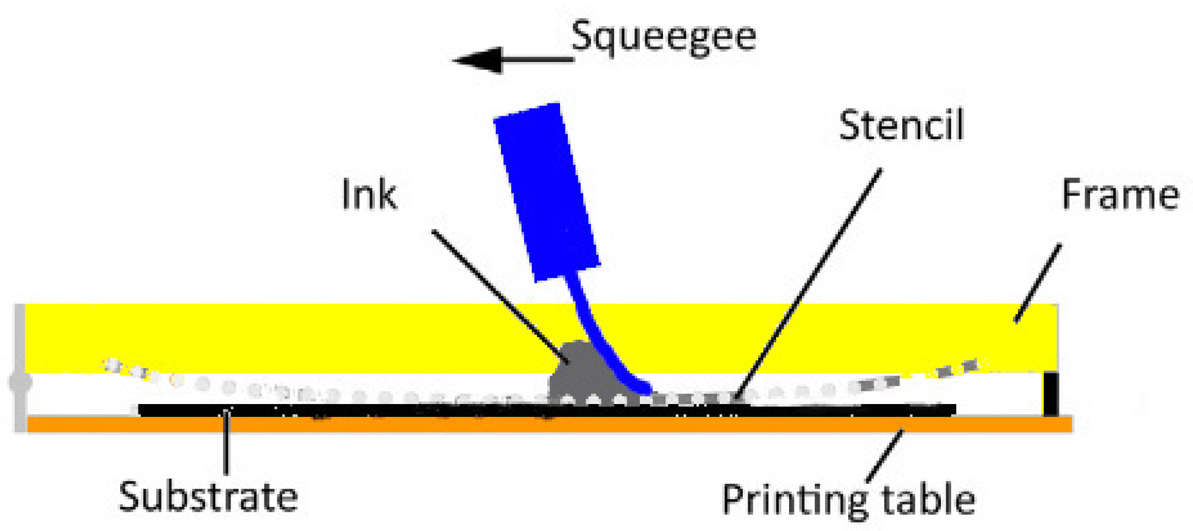
Figure 2.
Simulated lineic attenuation of a printed micro-strip line
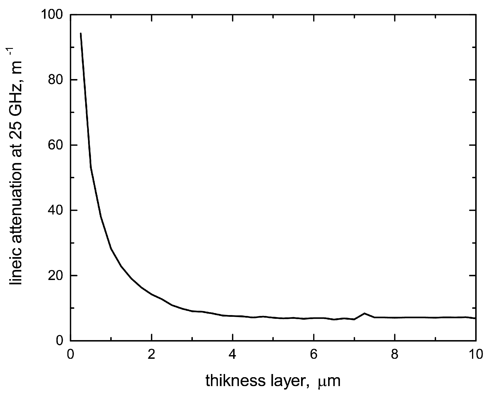
Figure 3.
The designed Quasi-Yagi-Uda antenna (a) complete ground plane, (b) patterned ground plane
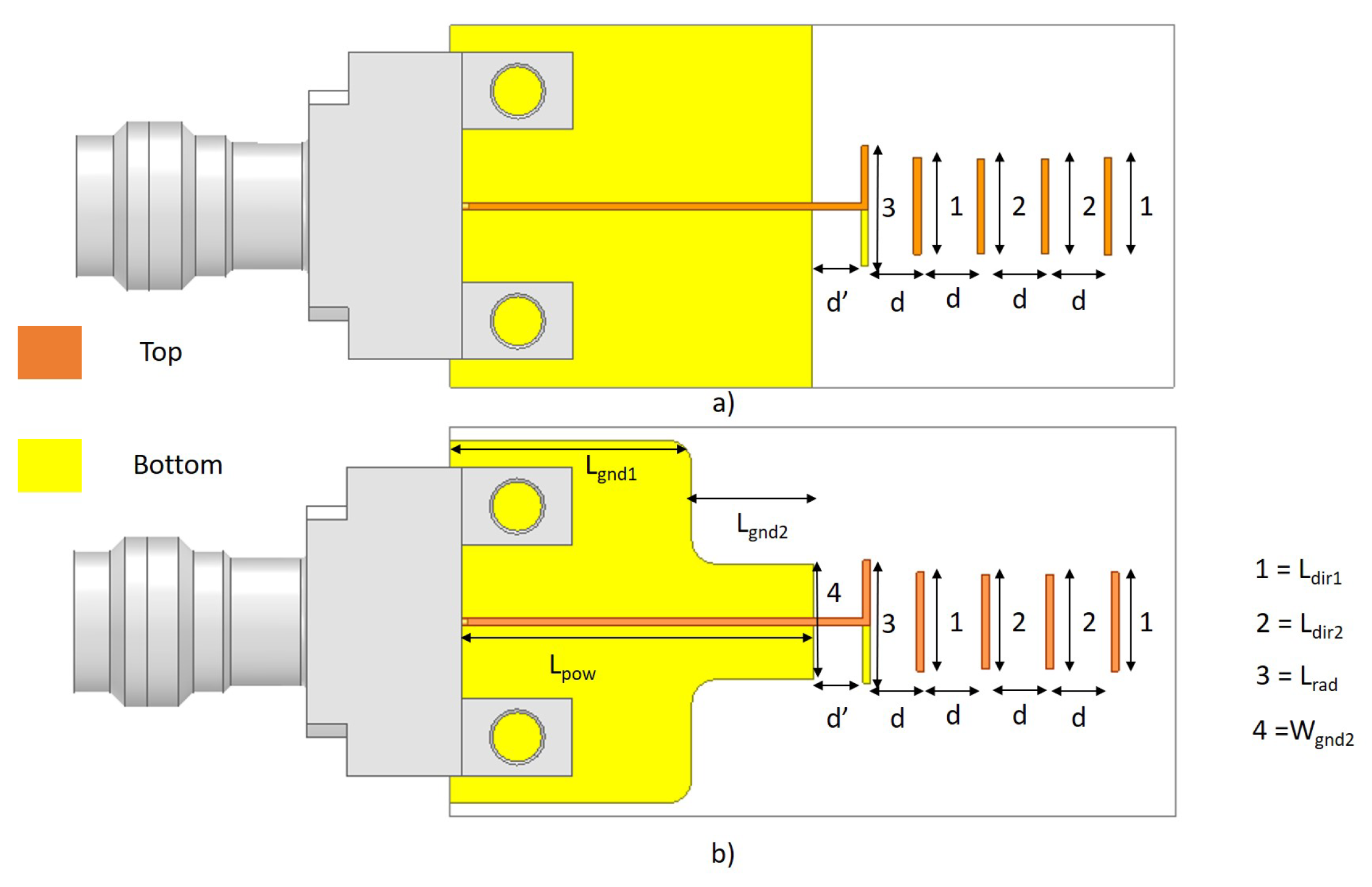
Figure 4.
Effects of on (a) realized gain, (b) matching of the proposed Quasi-Yagi-Uda screen printed antenna
Figure 4.
Effects of on (a) realized gain, (b) matching of the proposed Quasi-Yagi-Uda screen printed antenna
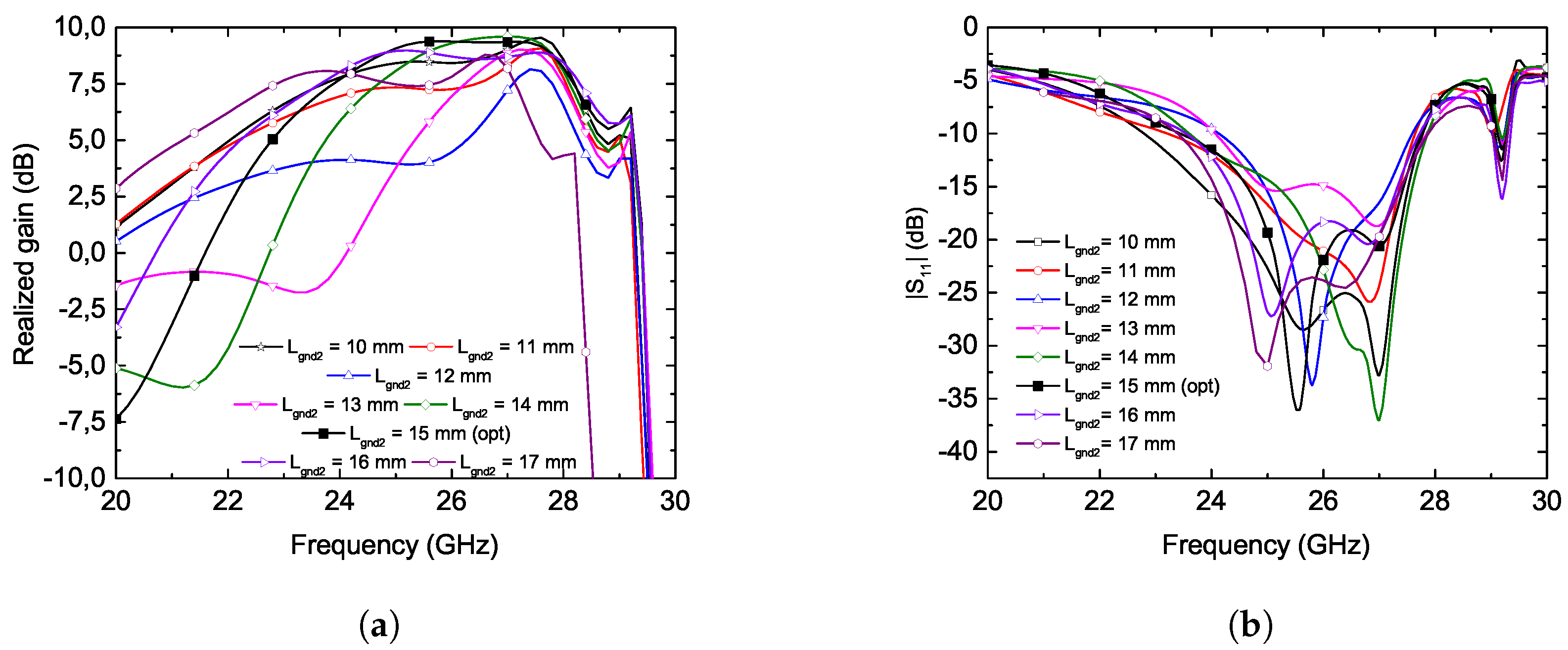
Figure 5.
Effects of on (a) realized gain, (b) matching of the proposed Quasi-Yagi-Uda screen printed antenna
Figure 5.
Effects of on (a) realized gain, (b) matching of the proposed Quasi-Yagi-Uda screen printed antenna
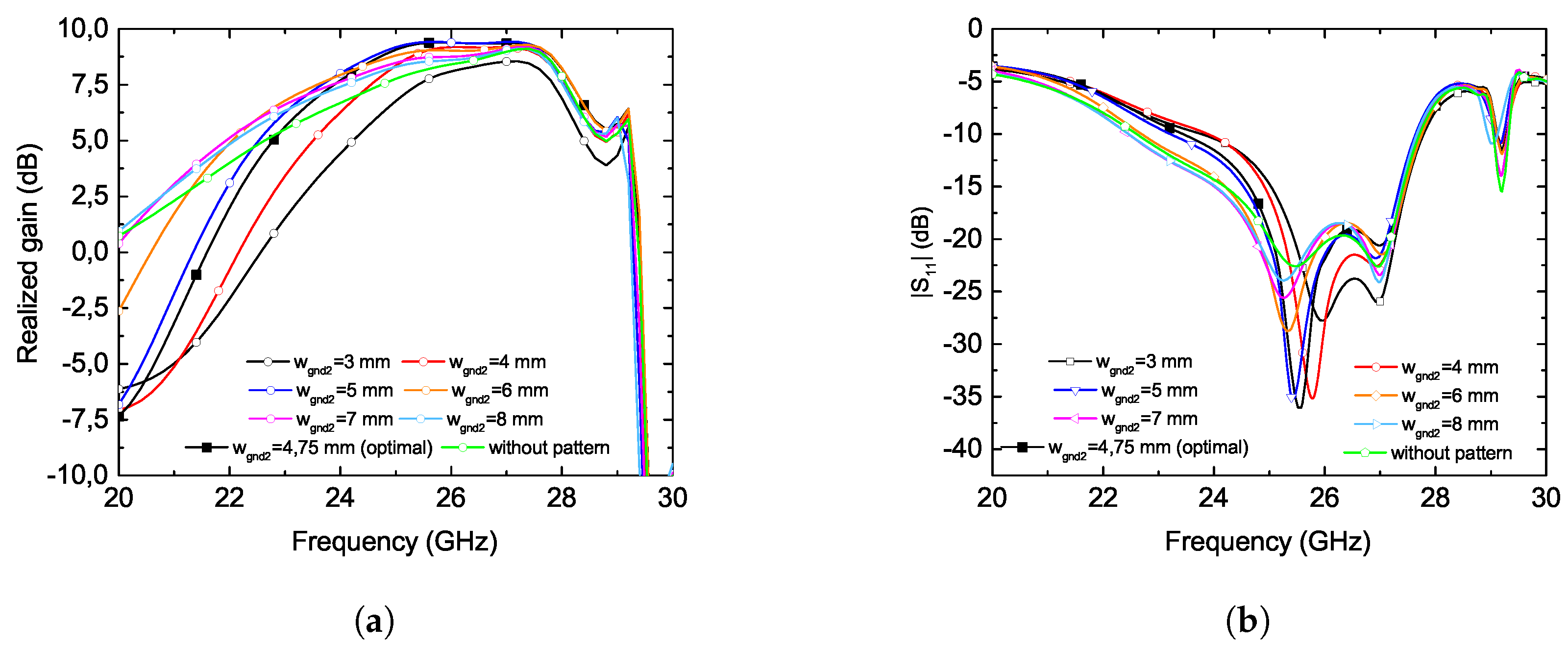
Figure 6.
Quasi-Yagi-Uda antenna simulated performances
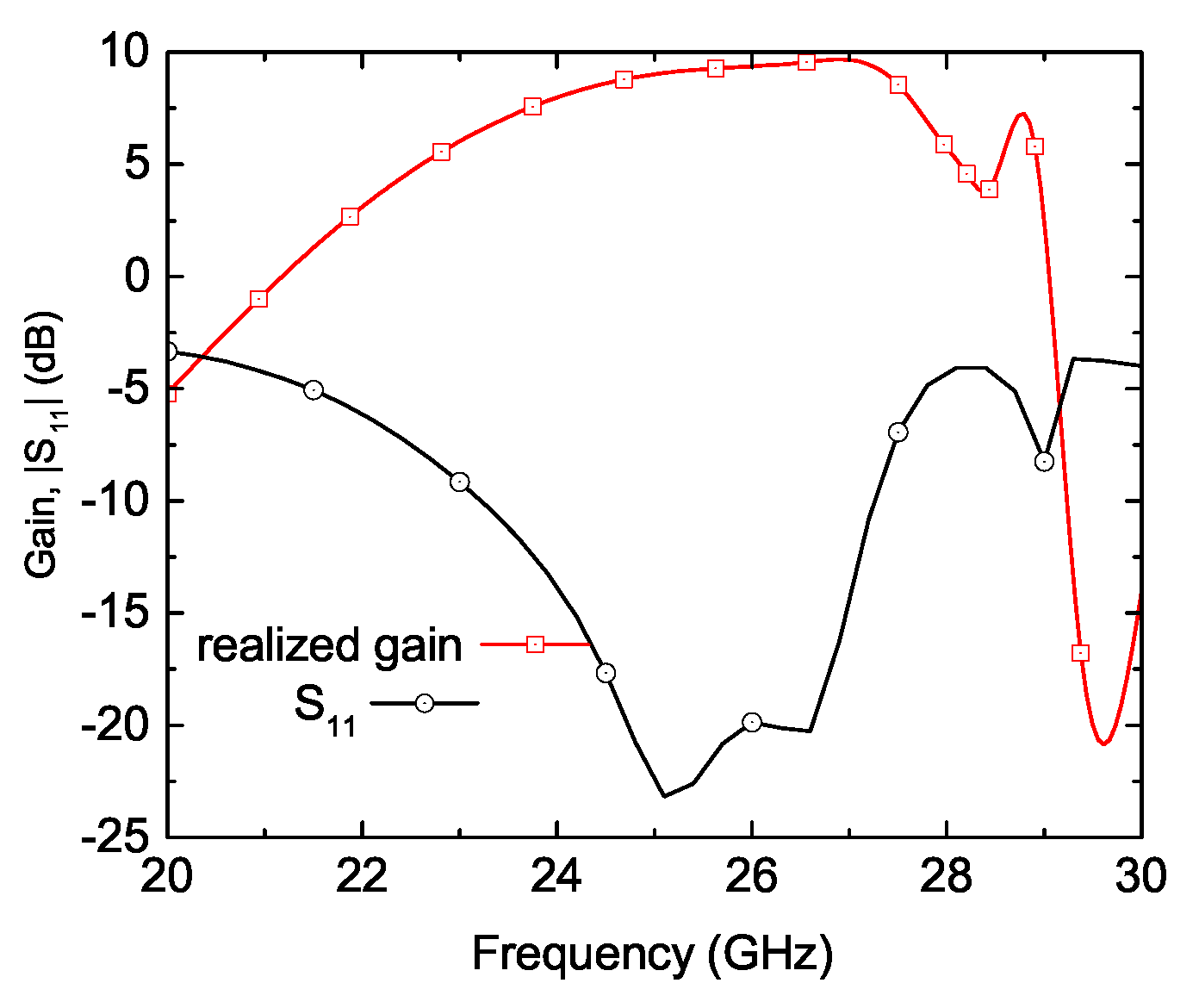
Figure 7.
Effects of the modified ground plane on the (a) E-plane and (b) H-plane cut of the radiation pattern of the Quasi-Yagi-Uda antenna at 26 GHz
Figure 7.
Effects of the modified ground plane on the (a) E-plane and (b) H-plane cut of the radiation pattern of the Quasi-Yagi-Uda antenna at 26 GHz
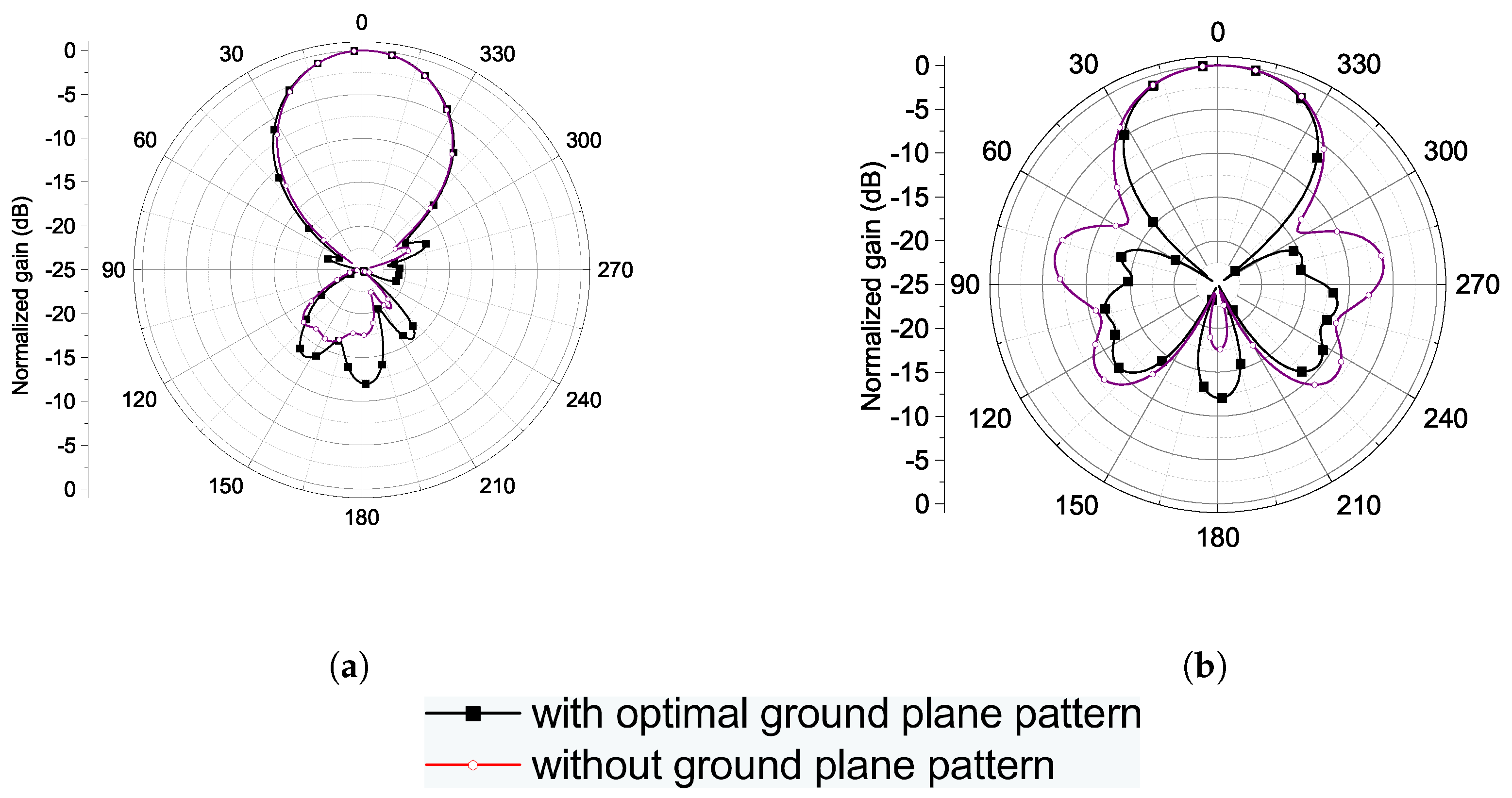
Figure 8.
Photograph of a screen-printed Quasi-Yagi-Uda antenna
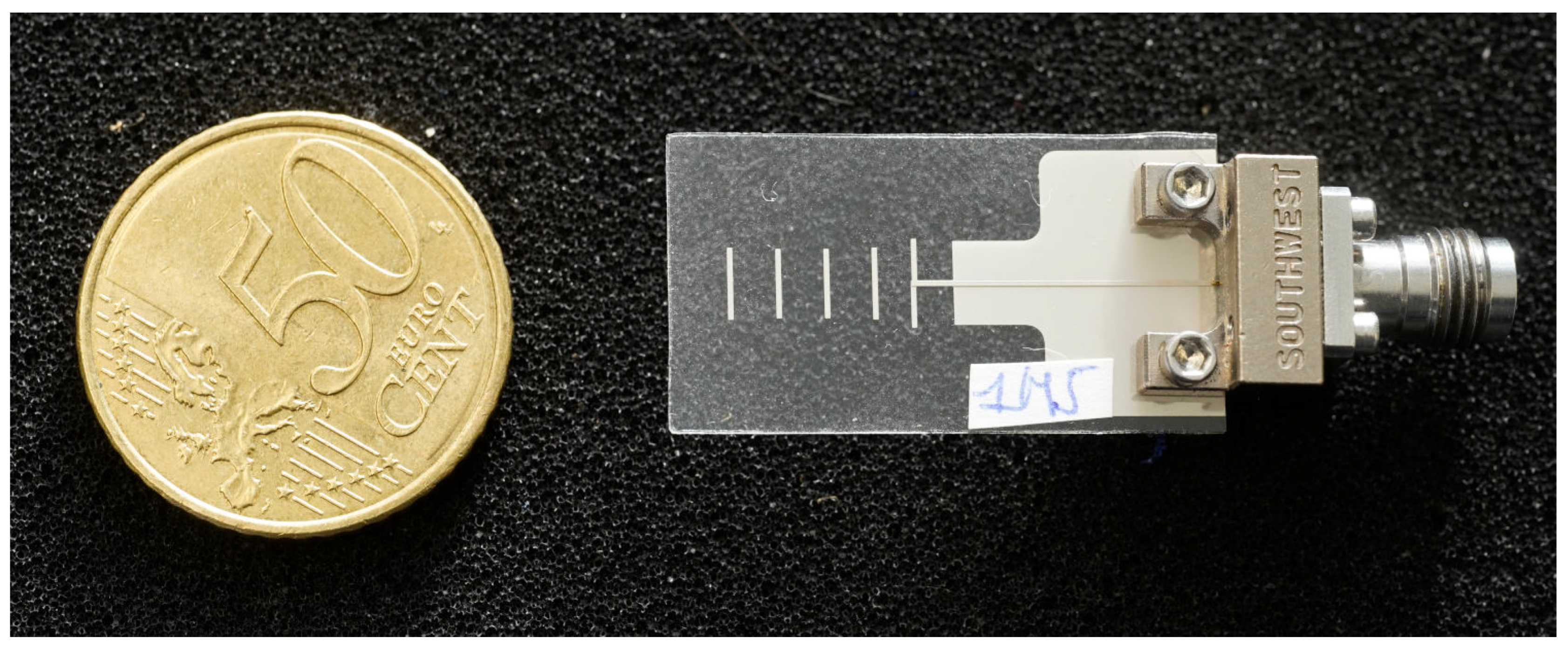
Figure 9.
(a) Measured gain for 24 screen-printed quasi-Yagi-Uda, (b) standard deviation on gain measurement for each sheet as function of the frequency
Figure 9.
(a) Measured gain for 24 screen-printed quasi-Yagi-Uda, (b) standard deviation on gain measurement for each sheet as function of the frequency
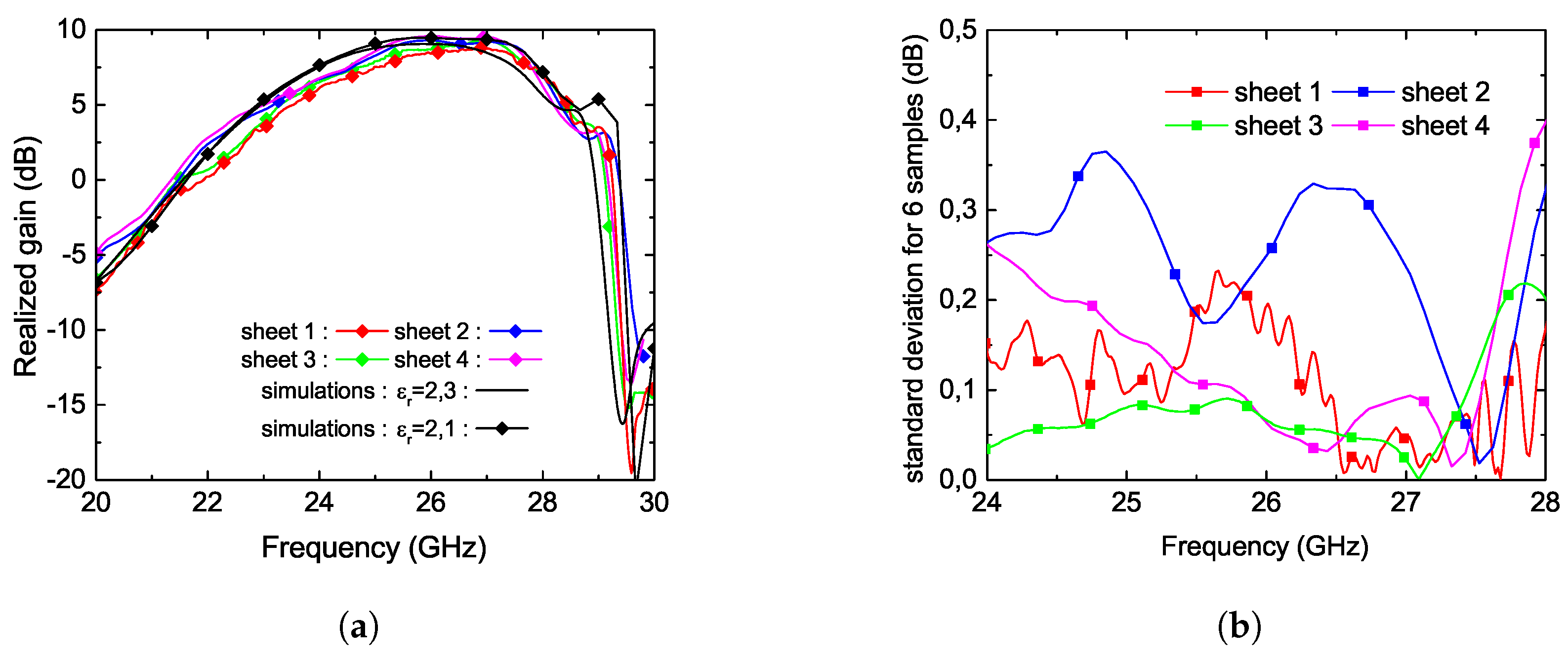
Figure 10.
(a) Measured for 24 screen-printed quasi-Yagi-Uda, (b) standard deviation on measurement for each sheet as function of the frequency
Figure 10.
(a) Measured for 24 screen-printed quasi-Yagi-Uda, (b) standard deviation on measurement for each sheet as function of the frequency
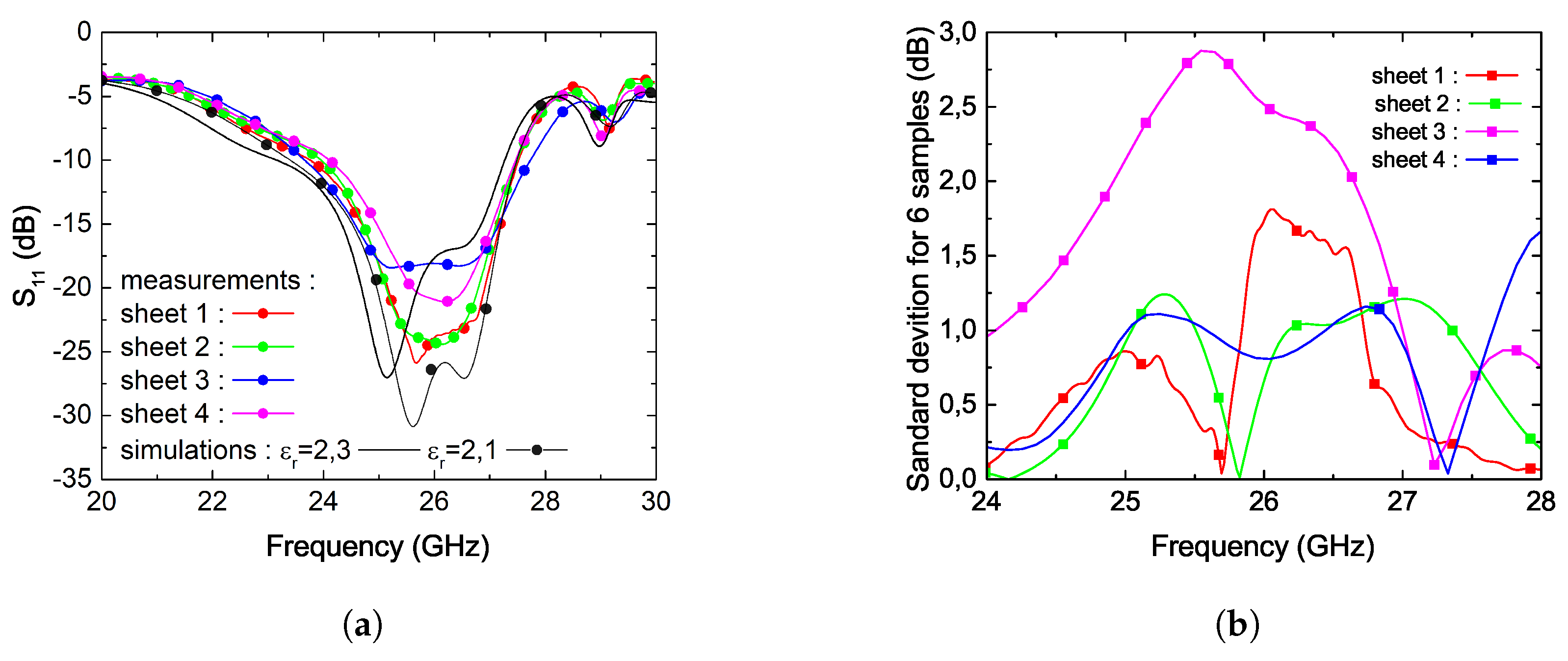
Figure 11.
Radiation pattern of Quasi-Yagi-Uda antenna at (a) 24.5 GHz, (b) 25 GHz, (c) 26 GHz and (d) 27 GHz.
Figure 11.
Radiation pattern of Quasi-Yagi-Uda antenna at (a) 24.5 GHz, (b) 25 GHz, (c) 26 GHz and (d) 27 GHz.
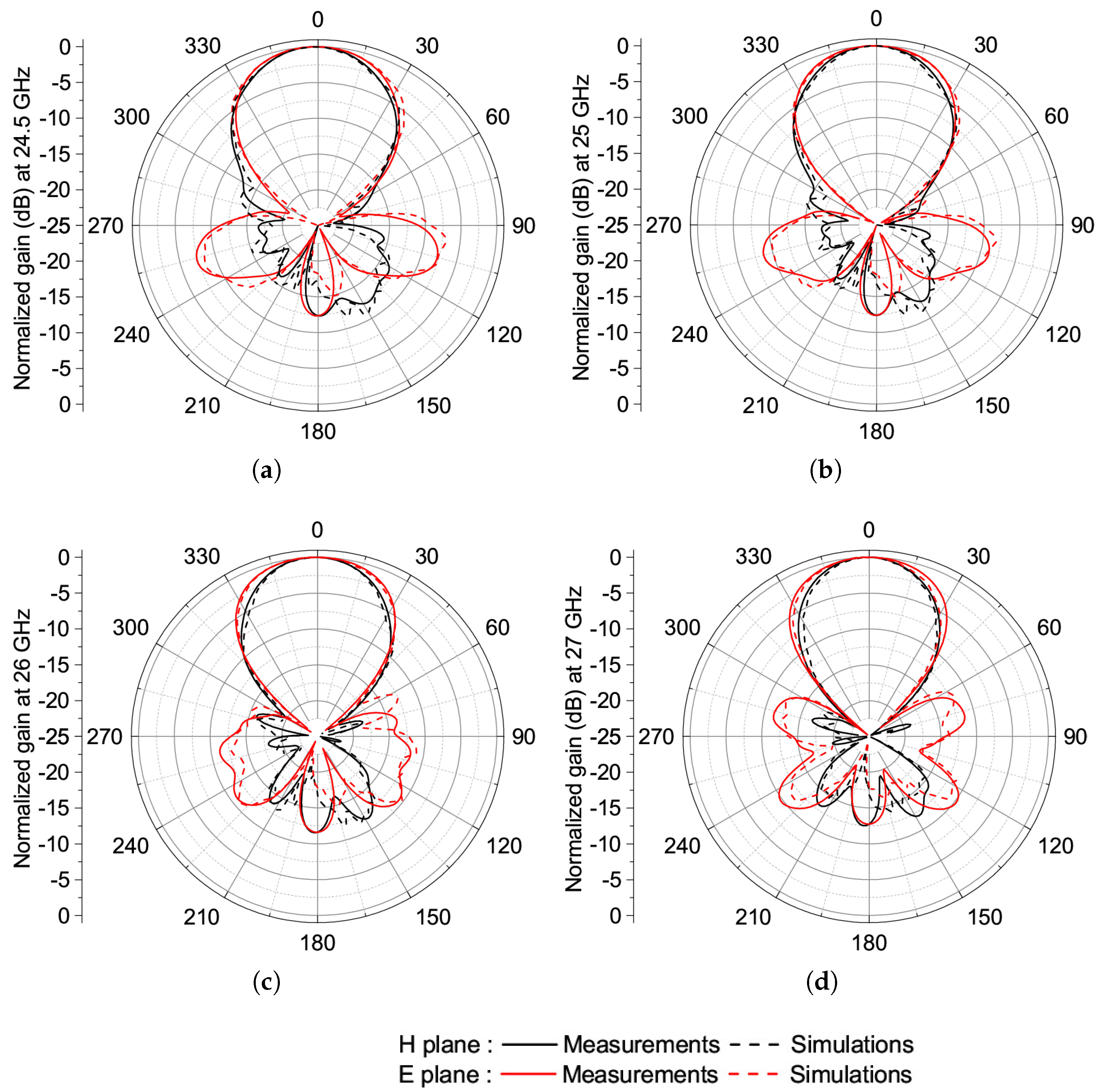
Figure 12.
(a) Top view of the modified wilkinson power divider (b) simulated S-parameters of a single wilkinson modified power divider as function of the frequency
Figure 12.
(a) Top view of the modified wilkinson power divider (b) simulated S-parameters of a single wilkinson modified power divider as function of the frequency
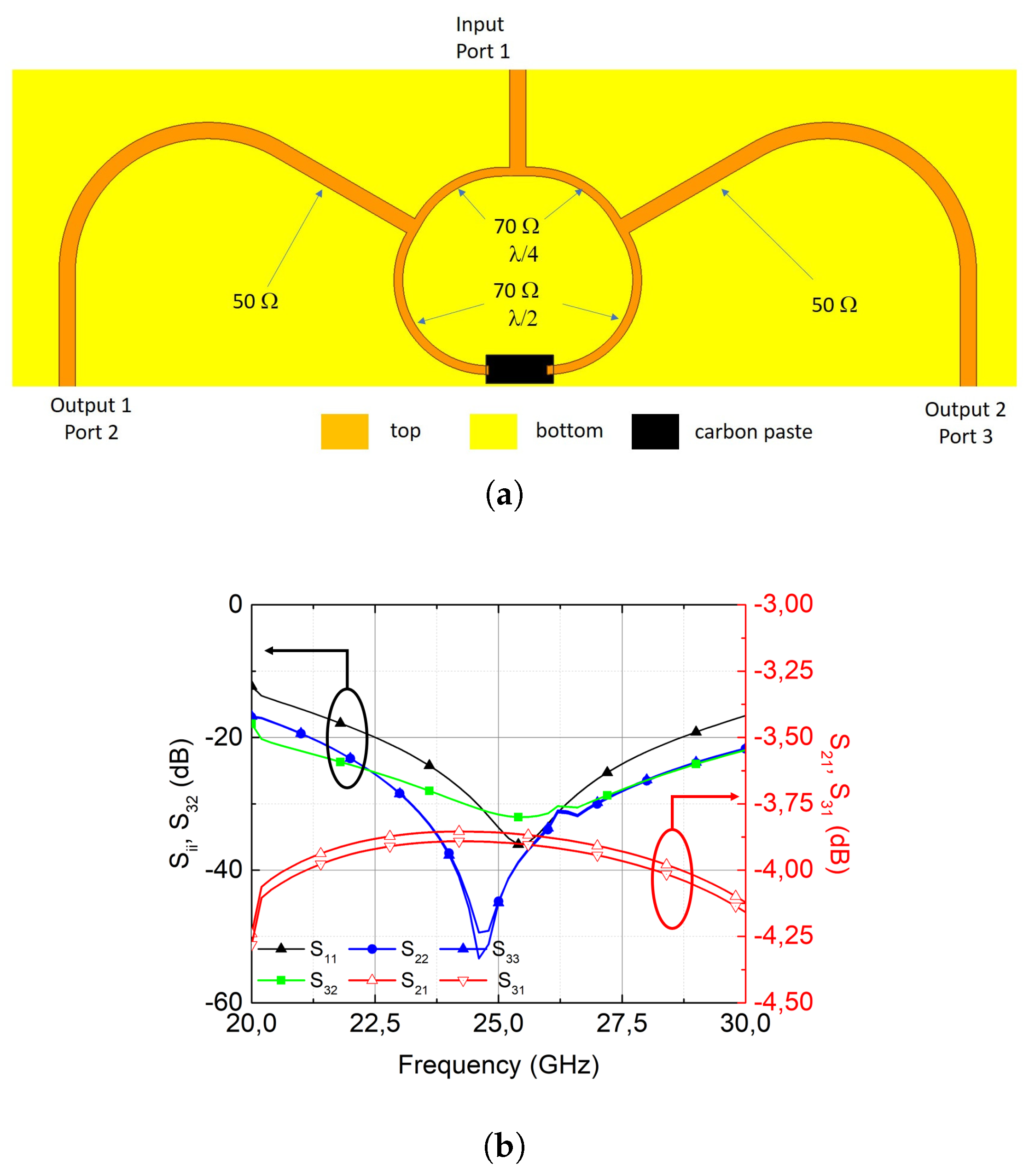
Figure 13.
Effect of array pitch on antenna array performances
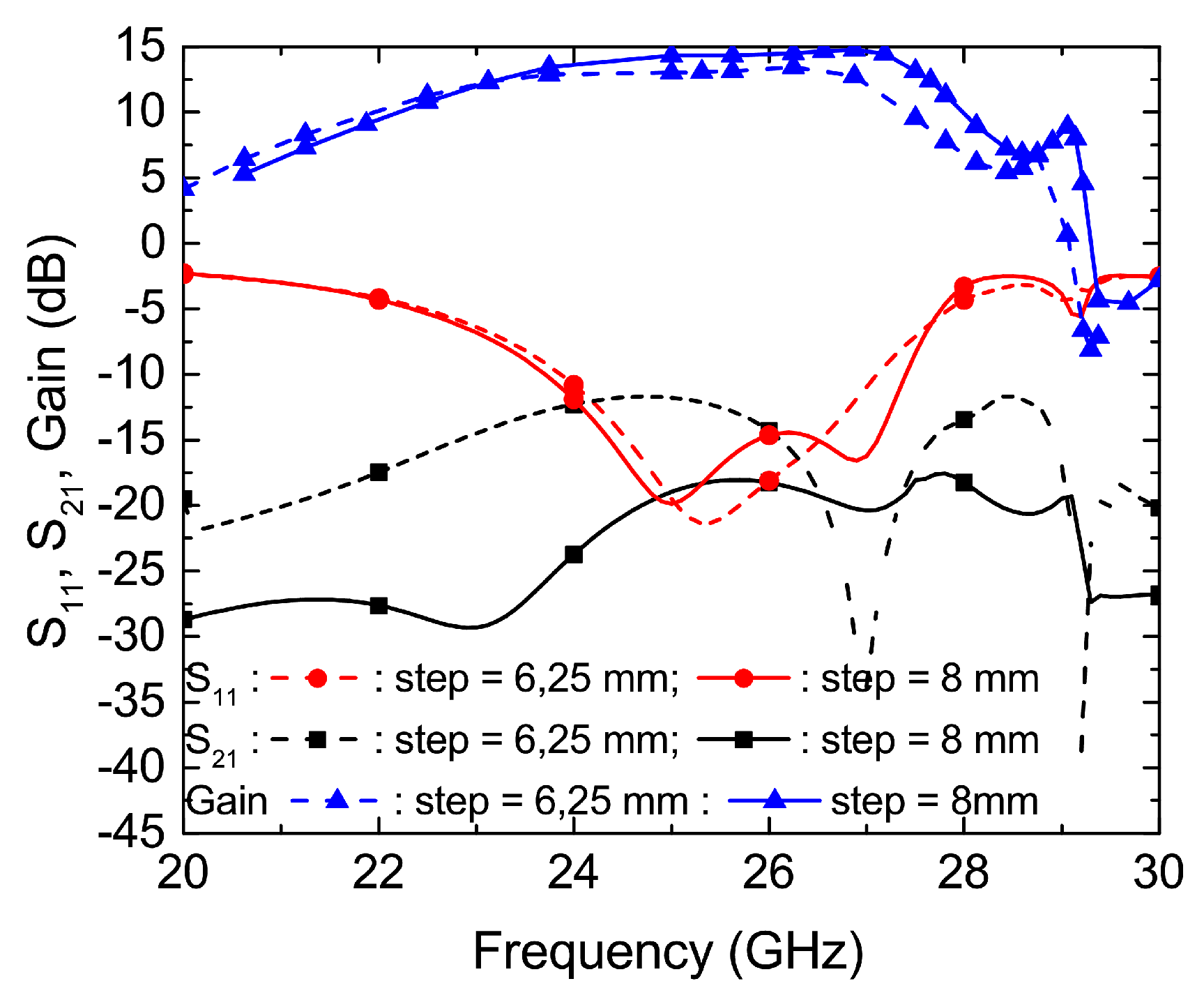
Figure 14.
(a) Top view of the 4x1 Quasi-Yagi screen-printed antenna array, (b) Simulation results of and gain for the 4x1 Quasi-Yagi Uda antenna array as function of the frequency
Figure 14.
(a) Top view of the 4x1 Quasi-Yagi screen-printed antenna array, (b) Simulation results of and gain for the 4x1 Quasi-Yagi Uda antenna array as function of the frequency
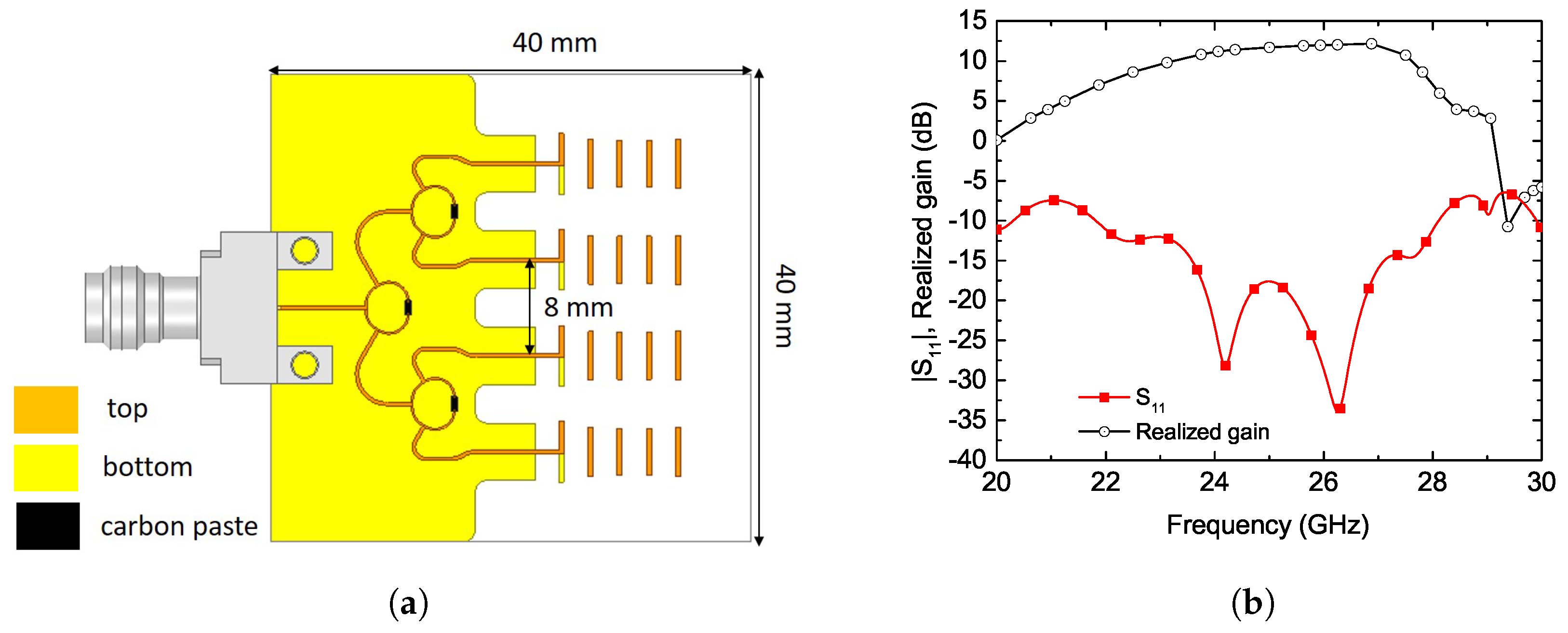
Figure 15.
Photograph of a screen printed Quasi-Yagi-Uda antenna array
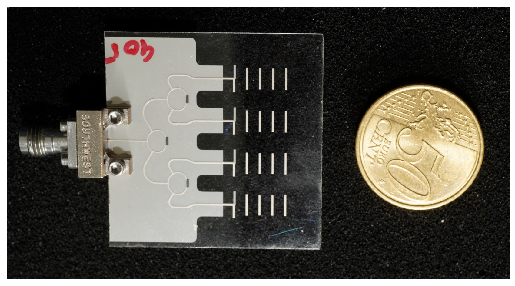
Figure 16.
(a) average per sheet of measured gain, (b) standard-deviation per sheet of measured gain
Figure 16.
(a) average per sheet of measured gain, (b) standard-deviation per sheet of measured gain
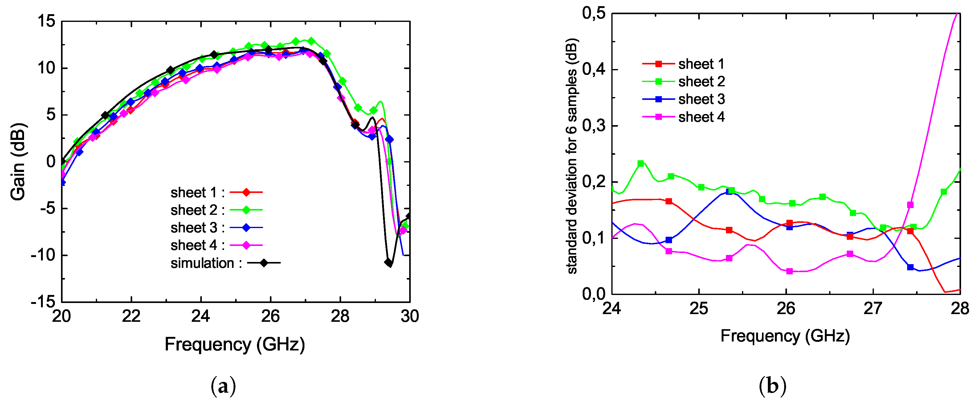
Figure 17.
(a) average per sheet of , (b) standard-deviation per sheet of
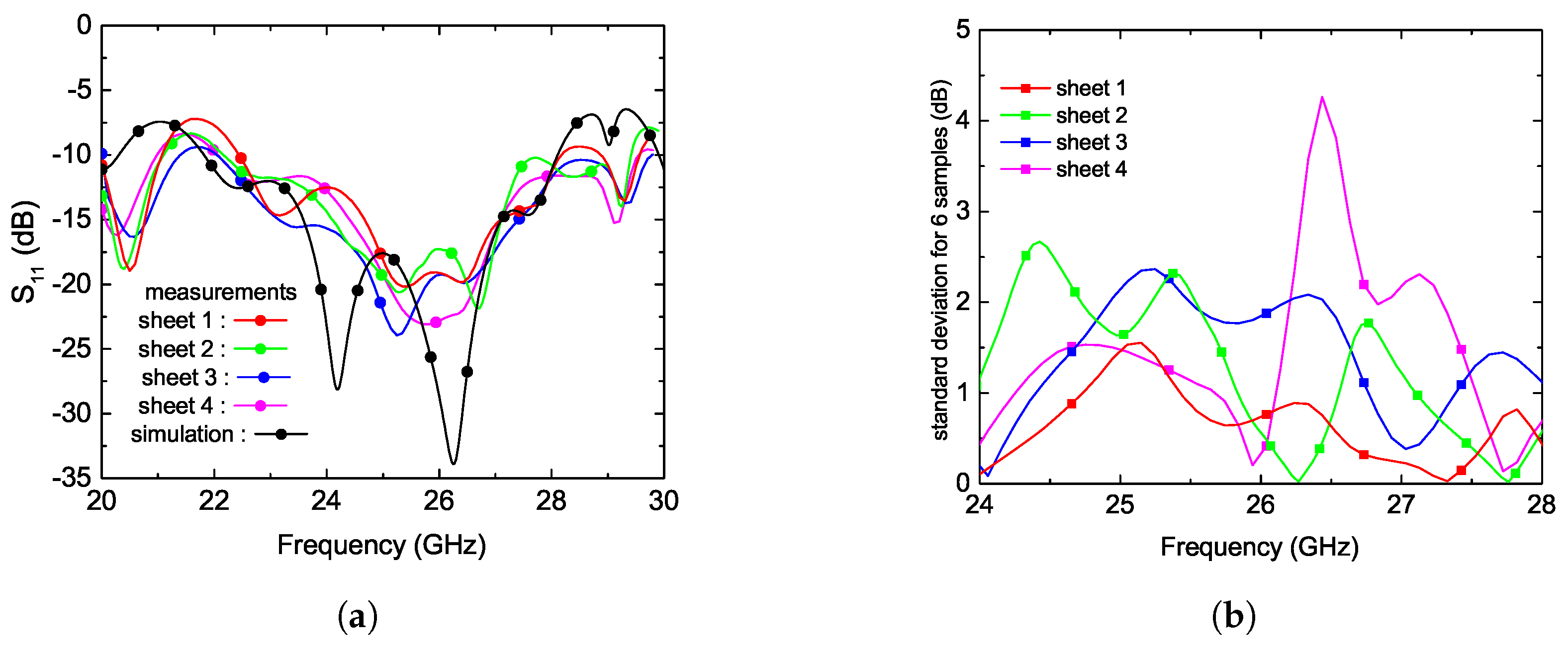
Figure 18.
Normalized radiation pattern at (a) 24.5 GHz, (b) 25 GHz, (c) 26 GHz and (d) 27 GHz
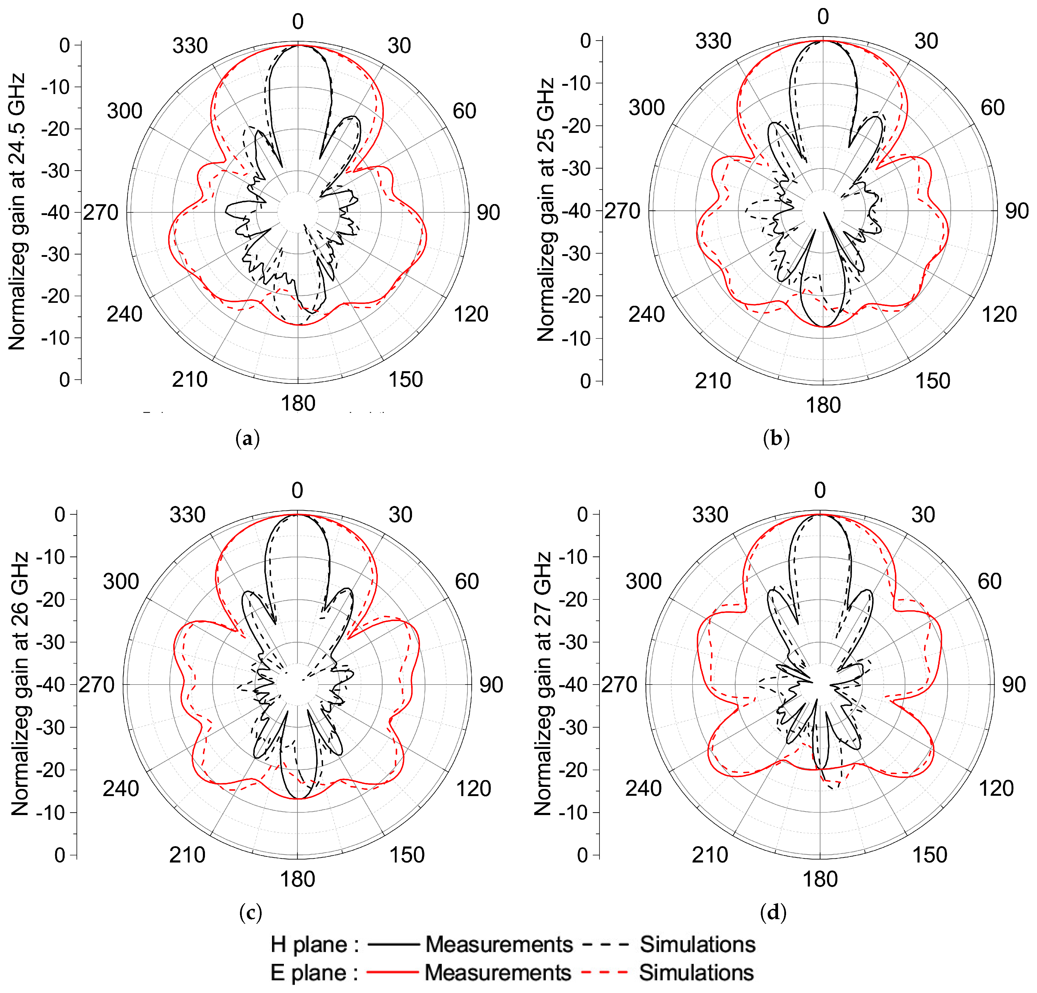

Table 1.
Properties of the silver ink
| Ink name | conductivity | thickness | |
|---|---|---|---|
| ECI1011 |
Table 2.
Geometrical parameters the elementary Yagi antenna.
| Parameter | value | Parameter | value |
|---|---|---|---|
| d | |||
Table 3.
Comparison with other published 5G 26 GHz Quasi-Yagi-Uda antennas.
| Ref | bandwidth | Gain | substrate | metallization | radiators | |
|---|---|---|---|---|---|---|
| This work | zeonor | silver ink | 4 | |||
| [21] | screen-printable ink | AgNW ink | 1 | |||
| [22] | Megtron6* | copper | 4 | |||
| [23] | Neltec NX9240* | copper | 5 | |||
| [17] | RO4350B* | - | 3 | |||
| [20] | MFLEX* | - | 3x2 | |||
| [24] | liquid crystal | copper | 3 |
* Standard PCB technology
Disclaimer/Publisher’s Note: The statements, opinions and data contained in all publications are solely those of the individual author(s) and contributor(s) and not of MDPI and/or the editor(s). MDPI and/or the editor(s) disclaim responsibility for any injury to people or property resulting from any ideas, methods, instructions or products referred to in the content. |
© 2025 by the authors. Licensee MDPI, Basel, Switzerland. This article is an open access article distributed under the terms and conditions of the Creative Commons Attribution (CC BY) license (http://creativecommons.org/licenses/by/4.0/).
Copyright: This open access article is published under a Creative Commons CC BY 4.0 license, which permit the free download, distribution, and reuse, provided that the author and preprint are cited in any reuse.


