
Submitted:
07 January 2026
Posted:
08 January 2026
You are already at the latest version
Abstract
In this work, we report a dual-mode ferroelectrically programmable on-chip antenna. The antenna is built on a silicon wafer using Complementary Metal-Oxide-Semiconductor (CMOS) processes and exhibits two programmable resonant modes: one in the super high frequency (SHF) range and one in the extremely high frequency (EHF) range. The SHF mode resonates at 8.5 GHz and exhibits ultrawideband (UWB) behavior, while the EHF mode resonates at 36.6 GHz. Both resonance frequencies can be tuned in a non-volatile fashion by controlling the ferroelectric polarization state of a Hafnium Zirconium Oxide (HZO) varactor monolithically integrated into the feed line. This programmability arises from the ferroelectric switching of the embedded HZO film, which results in a non-volatile variation of its permittivity upon application of a voltage pulse. Ferroelectric switching occurs at approximately ±3 V and induces maximum resonance frequency shifts of 381 MHz for the SHF mode and 3 GHz for the EHF mode, corresponding to fractional frequency changes of 4.5% and 8.3%, respectively. Unlike previously reported ferroelectrically tunable antennas, our reported antenna combines full integration, CMOS compatibility, higher operating frequency, compact footprint, and non-volatile programmability.
Keywords:
ferroelectric devices
; reconfigurable antennas
; ultrawideband antennas
; hafnium zirconium oxide
1. Introduction
Driven by the increasing need for service bands in fifth-generation (5G) communication systems and by the approaching sixth-generation (6G) era, wireless front-end designers face growing challenges to increase the data rates available for communication while preserving low power consumption [1]. Equipping radiofrequency front-ends (RFFEs) with programmable components is an effective approach to improve power efficiency, in particular through adaptive reconfiguration based on instantaneous power and communication requirements [2]. The development of reconfigurable ultrawideband (UWB) on-chip antennas is particularly important, as it can lead to the optimization of transceivers’ power efficiencies and throughput regardless of the active operating mode of power amplifiers (PAs) [3]. Similarly, developing these antennas would reduce self-interference coming from the impedance mismatch between PAs’ output impedance and antennas’ input impedance [4].
Among electrically reconfigurable antennas, different methods addressing frequency programmability were studied [5,6]. Due to its miniaturization potential and reduced parasitics [7,8], the monolithic integration of an antenna with a tunable reactance is considered one of the preferred strategies to achieve on-chip programmable antennas [9]. In this regard, the integration of antennas with microelectromechanical
34 systems (MEMS) [10,11], graphene [12] or metamaterials [13,14] has recently been proposed. However, the non-compact form factor, the high required voltage, or the challenging fabrication requirements make these existing methods hard to exploit, especially when adopting circuit elements manufactured using established Complementary Metal-Oxide-Semiconductor (CMOS) fabrication techniques [15]. Alternatively, the use of ferroelectric components to program antennas’ response has recently been proposed. In this regard, tunable antennas using (KTN) [16], (KNN) [17] and and (BST) as ferroelectric material have been previously reported. However, all these materials lack CMOS compatibility, which hinders their use in large-scale manufactured RFFEs.
Hafnium Zirconium Oxide (HZO), first discovered by Mueller et al. [18], has quickly become one of the most versatile ferroelectric materials [19]. Importantly, HZO is already available in CMOS foundries [20], and shows a significant ferroelectric remnant polarization [21] when its thickness is within a few tens of nanometers [22]. An extensive portion of its properties, such as the doping percentage [23], the mechanical stress effect of the electrodes [24], the switching speed [25], and the optimal film thickness [26,27], have been thoroughly investigated in the past. More recently, an initial investigation on the high-frequency properties of HZO varactors has been carried out [28], where capacitive tuning ranges as high as 15% and 11% were measured within the super (SHF) and extremely high frequency (EHF) ranges, respectively. Nonetheless, only a few tunable RF components leveraging the ferroelectric characteristics of HZO have been reported to date[29], mostly for wireless sensing [30,31] and analog computing [32,33].
In this work, we report a HZO-based ferroelectrically tunable RF antenna. The antenna consists of an on-chip monopole antenna embedding an HZO varactor in its feed-line, and is designed to exploit two electromagnetic modes for dual-mode operation. One mode, from now on labeled "the SHF mode", has a resonance frequency at 8.5 GHz, whilst the other mode, the "EHF mode", displays a resonance frequency at 36.6 GHz. The resonance frequency of both modes can be tuned by exploiting the ferroelectric properties of the varactor. In particular, the varactor shows a tunable capacitance when a biasing voltage is applied across its metallic plates, a feature that allows to modulate the electrical length of the feed line and, consequently, to shift the antenna’s resonance frequency of both modes.
Excitingly, we show here that this shift is non-volatile, allowing both resonance frequencies to be reprogrammed and to retain their values even when the varactor’s biasing voltage is removed. In fact, when a voltage above the coercive voltage of the HZO layer is applied across the varactor’s metallic plates, polarization switching of its HZO layer occurs. This switching results into a non-volative change in the dielectric permittivity of the HZO layer (e.g., the dielectric permittivity does not return to the initial value after removing the biasing voltage). Such ferroelectric polarization retention practically enables a programmability of the antenna’s resonance frequency that does not require the biasing voltage to be continuously connected to the varactor during the regular operation of the antenna. This, in turn, enables reduced power consumption in the biasing circuitry and suppresses any degradation in the antenna’s insertion loss due to feed-through of the RF power into the DC power line.
2. Materials and Methods
2.1. Antenna Design
The reported antenna is described in Figure 1. The antenna consists of a meander-line monopole [34], where indicates the electromagnetic wavelength. The choice of the monopole over the traditional dipole allows us to shrink the overall dimension of the antenna while maintaining the desired electrical length [35]. The antenna is composed of a patterned 100 nm-thick platinum (Pt) bottom electrode forming the meandered structure, in conjunction with a 20 nm-thick HZO layer and a 200 nm-thick gold (Au) top electrode. The whole antenna is built on a high-resistivity silicon (Si) wafer coated with a 150 nm thick thermal oxide layer. The antenna’s overall dimensions are 1.68 mm in length () and 1.5 mm in width (). The width of the meandered pattern is 360 m (), while the gaps are set to 300 m (). The antenna is fed with a 1080 m long () and 120 m wide () 50 coplanar waveguide (CPW)-to-microstrip transmission line hosting the varactor, which is directly connected to the ground-signal-ground probing pad used to drive the device.
The location of the varactor was chosen to maximize the change in the resonance frequency of both operating modes, which is induced by a variation of the varactor’s capacitance. This was done by placing the varactor at a position within its hosting microstrip line that shows large modal electric field values for both modes. All the antenna’s in-plane dimensions are listed in Table 1, together with the in-plane dimensions of the varactor ( and ). and are also important design parameters for the reported antenna. was chosen to ensure proper matching to 50 when no voltage is applied. In particular, through our optimization process based on finite element analysis (FEA) simulations, we found that an of 460 m ensured a return loss larger than 40 dB for the SHF mode and a return loss larger than 10 dB for the EHF mode. By contrast, was selected to match the size of the probes used to bias the varactor, ensuring reliable electrical contact to the top electrode in the Pt-HZO-Au junction region. The electrical access to the bottom metal plate was instead provided through a 45 m by 45 m via etched through the HZO layer. The position of the via (Figure 1a) did not appear to be critical in terms of return loss, according to FEA simulations.
2.2. HZO Material Characterization
The ferroelectric characterization of the varactor started by analyzing the electrical response of the ferroelectric layer embedded in our antenna (Figure 1a), and was performed through an AixACCT TF 2000 analyzer. The polarization state of the ferroelectric layer was controlled by applying a voltage between the top electrode and the bottom grounded plate through direct probing. First, we extracted the polarization vs. applied voltage (PV) characteristics of the deposited HZO layer by applying a 5 kHz voltage pulse with a triangular waveform (Figure 2a). We found a remnant polarization () of 24 C/cm2, which matches closely what found in previous work [22].
Later, we extracted the voltage-dependent capacitance values () of our varactor from capacitance vs. applied voltage (CV) measurements. We then computed the dielectric permittivity () of the deposited HZO film through the following equation:
where we refer to the HZO film thickness as and to the area of the overlap between the two metallic electrodes as . It is worth noting that the equation above is voltage-dependent, since HZO’s dielectric permittivity value varies when the film is biased.
Finally, the tuning range (TR) of the fabricated varactors, which represents the maximum degree of programmability achievable by the ferroelectric layer, was computed as reported in [28]:
where indicates the dielectric permittivity at the coercive voltage and refers to the dielectric permittivity at the maximum tunability of the HZO film.
The resulting dielectric permittivity vs. applied voltage measurement (Figure 2b) shows a distinctive ferroelectrically induced butterfly shape, exhibiting a maximum TR of 28%, with an of 44.9 and an of 32.3. The measured TR value is a significant improvement over the current state of the art (15%, as reported in [28]), showing the effectiveness of our in-house deposition method.
The as-deposited HZO layer exhibits a dielectric permittivity of 42 when no programming voltage is applied. As expected, the of the HZO layer is also voltage dependent. A slight imprint effect, which can be defined as the phenomenon where the coercive field is asymmetrically shifted along the voltage axis, can be identified in Figure 2b. As reported in [28,36], this phenomenon might be caused by the accumulation of space charges on one of the electrodes, thus increasing the pinching of the domain walls and inducing a Schottky effect [37].
2.3. Fabrication Process
The fabrication process of the proposed device is shown in Figure 3 [31] and adopts CMOS-compatible microfabrication techniques. A 10 nm-thick titanium (Ti) layer was sputtered on a thermal oxide-coated high resistivity silicon wafer for adhesion purposes. Afterwards, the 100 nm-thick meandered Pt bottom electrode was deposited through radio frequency (RF) sputtering. A bi-layer lift-off process was optimized to minimize fencing effects along the bottom electrode’s edges.
A 20 nm-thick ferroelectric HZO layer and a 3 nm-thick Al2O3 capping layer were subsequently deposited through atomic layer deposition (ALD). The thin HZO layer was grown by alternating pulses of tetrakis(dimethylamido)hafnium (TDMAHf) and tetrakis(dimethylamido)zirconium (TDMAZr) as precursors, each followed by water pulses as an O2 source. The Al2O3 layer was instead deposited using alternating pulses of trimethylaluminum (TMA) and water. A via was then etched in the HZO film through an inductively-coupled plasma (ICP) fluorine etch. Subsequently, a 200 nm-thick Au top electrode was deposited through e-beam evaporation. Finally, the chip hosting the fabricated devices was annealed through a rapid thermal annealing (RTA) processing step under N2 for 60 s at a temperature of 450 °C. A Scanning electron microscope (SEM) picture of the fabricated device is reported in Figure 4.
3. Results
The performance of the super high frequency (SHF) mode was characterized through direct wafer probing, using a ground-signal-ground (GSG) probe with a 150 m pitch. The parameters (Figure 6) were recorded using a Keysight P5008A vector network analyzer (VNA).
3.1. SHF Mode
This test was intended to measure the SHF mode’s resonance frequency for different partial and full polarization states of the varactor’s HZO layer. In this context and in line with prior work [31], we call partial polarization state a device’s state where only a fraction of the ferroelectric domains has been switched through the application of a triangular voltage cycle with the maximum value being lower than the coercive voltage of the HZO layer. First, we studied the effect of the ferroelectric polarization on the antenna’s resonance frequency by applying voltage pulses, ranging between -5 V and +5 V in steps of 0.5 V, across its varactor’s metal plates. To do so, we investigated the dependence of the resonance frequency of the SHF mode from the magnitude of the biasing voltage applied to polarize the varactor. The electrical response of the antenna was measured after executing each voltage step and following the removal of the voltage source. Our measurements (Figure 5) highlight a ferroelectrically-induced non-volatile programmability in the antenna’s resonance frequency, justifying the occurrence of a hysteresis behavior in the antenna’s resonance frequency vs. applied voltage profile.
It is worth emphasizing that our work is the first one, to our knowledge, that shows a non-volatile programmability of an antenna’s resonance frequency without the need of a continuous application of a DC bias. In fact, the embedded varactor requires only a single voltage pulse to achieve ferroelectric switching.
Figure 5 highlights the two operational points (A and B) showcasing the highest difference in resonance frequency and the corresponding programming voltages (3 V and -3.5 V). We report the SHF mode’s vs. frequency trends for such points in Figure 6. These trends were extracted after applying a single voltage pulse of 3 V for point A and -3.5 V for point B. After each set of measurements, we removed the voltage source and measured the antenna’s maximum resonance frequency shift without applying a continuous DC bias. The SHF mode displays a fractional bandwidth of 21% when considering a minimum return loss of 20 dB. Thus, according to [39], the antenna can be classified as UWB. To our knowledge, this is the first demonstration of a ferroelectrically programmable antenna with UWB capabilities.
Figure 6.
Measured and simulated parameters for point A (3 V) and point B (-3.5 V) for the SHF mode. Programming Voltages A and B mark the maximum ferroelectrically-induced frequency shift derived from the partial polarization experiment (see inset in Figure 5). This shift is obtained by modifying the polarization states of HZO’s domains.
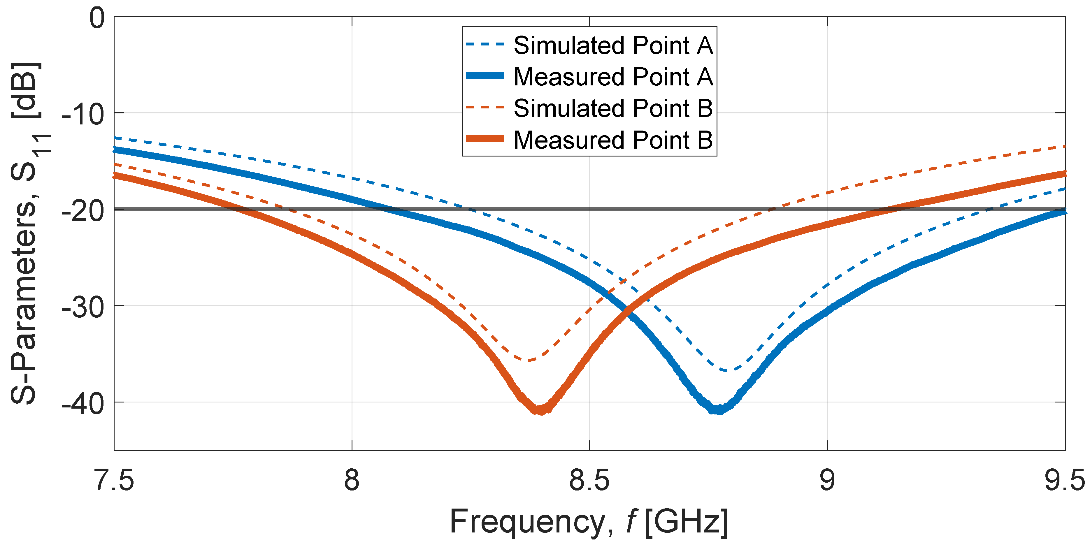
Evidently, the SHF mode shows resonance frequencies of 8.78 GHz and 8.399 GHz at points A and B, respectively. The measured frequency shift between the two points is 381 MHz, corresponding to a fractional frequency change (FFC) of 4.5%. The FFC between the lowest () and the highest () experimentally measured resonance frequencies at different applied voltages was computed as reported in [17]:
It is worth noting that the measured trends in Figure 6 closely match the corresponding simulated trends. These simulations were extracted by combining the results of our FEA model with the measured equivalent R-C circuit of the varactor. Furthermore, our FEA simulation assumed a perfectly conductive grounded backside plane, which is necessary to frame the metallic chuck of the RF-characterization setup.
We also experimentally extracted the gain of our SHF mode at points A and B and compared it with the expected values according to our circuit and FEA simulations (see Figure 6). The measured gain was extracted in an uncontrolled electromagnetic setting by wire-bonding our antenna to a printed
circuit board (PCB) and by using a commercial UWB transmitting antenna (DEEPACE Wideband Omnidirectional Antenna UWB-2) with fully-characterized gain vs. frequency trend. A picture of our experimental setup is reported in the inset of Figure 7. We found that the SHF mode exhibits a maximum gain of -4 dBi and -7.5 dBi at points A and B, respectively. The difference in gain for the two programming voltages originates from the different resistances of the varactor in the two partial polarization states. We attribute the discrepancies between the measured and simulated gains in Figure 7 to parasitics from the PCB used for gain characterization.
Next, we extracted the SHF mode’s normalized radiation diagrams (Figure 8) at the on-chip antenna’s resonance frequencies measured at points A and B (see Figure 6). A variation as big as 4 dB between the two ferroelectric polarization states of the HZO layer can be found in the two plots, suggesting a degree of programmability in the radiation patterns that was also adequately captured in the simulations. Overall, the E-plane pattern exhibits a multi-lobed structure while the H-plane pattern shows a more directive response.
3.2. EHF Mode
In this section, we experimentally demonstrated that the ferroelectric, non-volatile programmability reported for the SHF mode can be maintained and even improved at EHF frequencies[40]. As done for the SHF mode, the performance of the EHF mode was characterized through direct wafer probing, using a GSG probe with a 150 m pitch. The parameters (Figure 6) were recorded using a Keysight P5008A VNA.
The two operational points showcasing the highest difference in resonance frequency (A and B) for the EHF mode and the corresponding programming voltages (3 V and -3 V) are reported in Figure 9. As observed for the SHF mode, the applied programming voltage generates a ferroelectrically-induced hysteresis on the resonance frequency of the antenna between different partial polarization states. We also report the EHF mode’s vs. frequency trends for such points in Figure 10. These trends were extracted after applying a single voltage pulse of 3 V for point A and -3 V for point B. Similarly to the SHF mode, the antenna’s maximum resonance frequency shift was measured without applying a continuous DC bias.
The reported mode shows resonance frequencies of 37.957 GHz and 34.938 GHz at points A and B, respectively. The measured frequency shift between the two points is 3.019 GHz, corresponding to a fractional frequency change (FFC) of 8.3%, as computed through Equation 3. The antenna’s vs. frequency trends at the two different polarization states suggest a splitting of the electromagnetic mode. In fact, point A showcases one single resonance at 37.957 GHz, while point B exhibits two resonances (one at 34.938 GHz and the other at 40.283 GHz). The fractional bandwidth of the EHF mode, when considering a maximum allowed return loss of 6 dB, is 8% for point A and 3.5% for point B. Such a behavior was matched through a combination between FEA and circuital simulations. We observed the same splitting of the mode in the FEA simulated polarization states by adding a series inductance of 0.18 nH, which represents the expected sheet inductance of the probing pads. This value was derived from the ground pad structure, to compensate for effects that were not adequately captured in our FEA framework. It is important to highlight that we successfully recreated the experimentally measured vs. frequency trends for both polarization states by using the same series inductance value.
We then extracted the gain of the EHF mode for the polarization states A and B through the same experimental setup used for the SHF mode. The same considerations regarding the discrepancies between measured and simulated gain values drawn for the SHF mode can be extended here as well. Figure 11 compares the simulated and measured gain for the two polarization states (Points A and B) over the 30–41 GHz range. Both experimental polarization states follow a similar spectral trend, exhibiting a maximum gain of about 5 dBi for Point A and 4 dBi for Point B. The differences between the experimental curves, especially around 38.5 GHz, indicate the presence of polarization-dependent variations in gain magnitude across the band.
We also extracted the EHF mode’s normalized radiation diagrams (Figure 12) at the resonance frequencies measured at points A and B (see Figure 10). We found a nearly omnidirectional trend for the E-plane and a more directive response for the H-plane. As observed for the SHF mode, the radiation diagrams at points A and B exhibit polarization-dependent variations, which arise from the different polarization states of the HZO layer and are adequately reproduced by the FEA simulations. Among them, the most meaningful variation is highlighted in the E-plane plot (Figure 12a), where a 15 ° shift of the maximum gain can be observed.
4. Discussion
A comparison between this work and other ferroelectric-based reconfigurable antennas is presented in Table 2. The reported HZO-based antenna shows a smaller area and requires a significantly lower voltage to achieve ferroelectric switching compared to most reported counterparts. Together with the overall CMOS compatibility and low power consumption, the non-volatile programmability of the presented HZO-based device offers strong advantages over the BST, KNN, and KTN counterparts. Such a feature enables our antenna to retain its programmed resonance frequency value without having to continuously apply a bias, since the embedded varactor can achieve ferroelectric switching even with a single pulse. Furthermore, the lack of continuous bias relaxes the design constraints of electrostatic discharge protection circuits [41].
It is worth adding that, to the best of our knowledge, our device is the first ferroelectrically programmable antenna with UWB capabilities ever reported. Compared to another HZO-based device reported in the literature [21], this design exhibits a more compact form factor (area of only 6.5 mm2), non-volatile programmability of the resonance frequency, and a fractional frequency change of 4.5% for the SHF mode and 8.3% for the EHF mode, which is more than four times the one found in [21].
5. Conclusions
In this work, we present a ferroelectrically programmable on-chip dual-mode antenna. The proposed design combines miniaturization and ferroelectrically-derived programmability, monolithically integrating an HZO varactor into the transmission line of a meandered monopole and covering a much smaller on-chip area than its state-of-the-art counterparts.
Owing to the ferroelectric properties of the nanometer-thick HZO film, the reported antenna shows significant ferroelectric programmability, resulting in 4.5% and 8.3% fractional frequency shift of its two resonant modes without having to continuously apply DC voltages. To the best of our knowledge, the EHF mode represents the highest operating frequency for a ferroelectrically programmable antenna reported to date. Furthermore, we demonstrated the first ferroelectrically programmable mode with UWB capabilities. The combination of compact size, CMOS compatibility, UWB technology, high frequency of operation, non-volatile programmability, and low programming voltage marks a significant improvement over similar state-of-the-art devices. This frames HZO-based programmable antennas as promising candidates for future 5G and 6G-grade chip-scale transceivers.
Author Contributions
Conceptualization, S.Q., N.C. and C.C.; experimental methodology, S.Q., N.C. and O.K.; software, S.Q. and N.C.; experimental validation, S.Q. and S.B.; data curation, S.Q. and S.B.; writing—original draft preparation, S.Q. and C.C.; writing—review and editing, N.C., S.B., O.K., V.P., L.C., B.D. and J.M.J.; funding acquisition, J.M.J., V.P., B.D., and C.C. All authors have read and agreed to the published version of the manuscript.
Funding
This work has been supported by the U.S. Air Force Office of Scientific Research (AFOSR), award FA9550-23-1-0254.
Data Availability Statement
The data presented in this study are available upon request from the authors.
Conflicts of Interest
The authors declare no conflicts of interest.
References
- Akyildiz, I.F.; Kak, A.; Nie, S. 6G and Beyond: The Future of Wireless Communications Systems. IEEE Access 2020, 8, 133995–134030. [CrossRef]
- Haupt, R.L.; Lanagan, M. Reconfigurable Antennas. IEEE Antennas and Propagation Magazine 2013, 55, 49–61. [CrossRef]
- Park, S.; Woo, J.L.; Kim, U.; Kwon, Y. Broadband CMOS Stacked RF Power Amplifier Using Reconfigurable Interstage Network for Wideband Envelope Tracking. IEEE Transactions on Microwave Theory and Techniques 2015, 63, 1174–1185. [CrossRef]
- Kumar, O.P.; Kumar, P.; Ali, T.; Kumar, P.; Vincent, S. Ultrawideband Antennas: Growth and Evolution. Micromachines 2022, 13. [CrossRef]
- Christodoulou, C.G.; Tawk, Y.; Lane, S.A.; Erwin, S.R. Reconfigurable antennas for wireless and space applications. Proceedings of the IEEE 2012, 100, 2250–2261. [CrossRef]
- García, E.; Andújar, A.; Anguera, J. Overview of Reconfigurable Antenna Systems for IoT Devices. Electronics 2024, 13, 3988. [CrossRef]
- Colombo, L.; Guida, J.; Casilli, N.; Tetro, R.; Kaya, O.; Galanko-Klemash, M.E.; Bedair, S.S.; Ghosh, S.; Cassella, C.; Rinaldi, M. Monolithic Integration of X-cut Leaky SAWs and Electrically Small Antennas for RF Passive Wireless Sensors. In Proceedings of the 2023 IEEE International Ultrasonics Symposium (IUS). IEEE, 2023, pp. 1–4.
- Quaresima, S.; Giribaldi, G.; Petrov, V.; Davaji, B.; Jornet, J.M.; Colombo, L.; Rinaldi, M.; Cassella, C. On-chip mmWave Antennas on a Piezoelectric ScAlN-Si Platform for 6G-grade Internet of Things. In Proceedings of the 2024 IEEE International Symposium on Antennas and Propagation and INC/USNC-URSI Radio Science Meeting (AP-S/INC-USNC-URSI). IEEE, 2024, pp. 2171–2172.
- Yordanov, H.; Poulkov, V.; Russer, P. On-chip monolithic integrated antennas using CMOS ground supply planes. IEEE Transactions on Components, Packaging and Manufacturing Technology 2016, 6, 1268–1275. [CrossRef]
- Erdil, E.; Topalli, K.; Unlu, M.; Civi, O.A.; Akin, T. Frequency Tunable Microstrip Patch Antenna Using RF MEMS Technology. IEEE Transactions on Antennas and Propagation 2007, 55, 1193–1196. [CrossRef]
- Anagnostou, D.E.; Zheng, G.; Chryssomallis, M.T.; Lyke, J.C.; Ponchak, G.E.; Papapolymerou, J.; Christodoulou, C.G. Design, fabrication, and measurements of an RF-MEMS-based self-similar reconfigurable antenna. IEEE transactions on antennas and propagation 2006, 54, 422–432. [CrossRef]
- Dragoman, M.; Neculoiu, D.; Bunea, A.C.; Deligeorgis, G.; Aldrigo, M.; Vasilache, D.; Dinescu, A.; Konstantinidis, G.; Mencarelli, D.; Pierantoni, L.; et al. A tunable microwave slot antenna based on graphene. Applied Physics Letters 2015, 106, 153101, [https://pubs.aip.org/aip/apl/article-pdf/doi/10.1063/1.4917564/14313634/153101_1_online.pdf]. [CrossRef]
- Zhu, H.; Cheung, S.; Liu, X.; Yuk, T. Design of polarization reconfigurable antenna using metasurface. IEEE transactions on antennas and propagation 2014, 62, 2891–2898. [CrossRef]
- Bayatpur, F.; Sarabandi, K. A Tunable Metamaterial Frequency-Selective Surface With Variable Modes of Operation. IEEE Transactions on Microwave Theory and Techniques 2009, 57, 1433–1438. [CrossRef]
- Ahmed, A.; Goldthorpe, I.A.; Khandani, A.K. Electrically tunable materials for microwave applications. Applied Physics Reviews 2015, 2, 011302, [https://pubs.aip.org/aip/apr/article-pdf/doi/10.1063/1.4906255/13715835/011302_1_online.pdf]. [CrossRef]
- Cissé, F. Dispositifs hyperfréquences et antennes périodiques reconfigurables à base de films minces ferroélectriques des systèmes KTN-KNN. PhD thesis, Rennes 1, 2017.
- Aspe, B.; Castel, X.; Demange, V.; Députier, S.; Bouquet, V.; Benzerga, R.; Sauleau, R.; Guilloux-Viry, M. Frequency-Tunable Slot-Loop Antenna Based on KNN Ferroelectric Interdigitated Varactors. IEEE Antennas and Wireless Propagation Letters 2021, 20, 1414–1418. [CrossRef]
- Müller, J.; Böscke, T.; Bräuhaus, D.; Schröder, U.; Böttger, U.; Sundqvist, J.; Kücher, P.; Mikolajick, T.; Frey, L. Ferroelectric Zr0. 5Hf0. 5O2 thin films for nonvolatile memory applications. Applied Physics Letters 2011, 99. [CrossRef]
- Kim, S.J.; Mohan, J.; Summerfelt, S.R.; Kim, J. Ferroelectric Hf 0.5 Zr 0.5 O 2 thin films: A review of recent advances. Jom 2019, 71, 246–255. [CrossRef]
- Perera, A.; Quach, T.; Shen, J.; Njoka, S.M.; Drees, A.; Chakravarty, S. Silicon Microring Resonator Integrated Hafnium Zirconium Oxide Ferrophotonic Non-Volatile Memory. ACS Photonics 2025, 12, 4524–4533. [CrossRef]
- Aldrigo, M.; Tasolamprou, A.C.; Vasilache, D.; Kafesaki, M.; Iordanescu, S.; Nastase, F.; Dragoman, M. Tunable microwave dual-band patch antenna through integration of metamaterials and nanoscale ferroelectrics. Phys. Rev. Appl. 2023, 20, 044067. [CrossRef]
- Casilli, N.; Kaya, O.; Kaisar, T.; Davaji, B.; Feng, P.X.L.; Cassella, C. Nonvolatile State Configuration of Nano-Watt Parametric ISING Spins Through Ferroelectric Hafnium Zirconium Oxide MEMS Varactors. In Proceedings of the 2023 IEEE 36th International Conference on Micro Electro Mechanical Systems (MEMS), 2023, pp. 511–514. [CrossRef]
- Muller, J.; Boscke, T.S.; Schroder, U.; Mueller, S.; Brauhaus, D.; Bottger, U.; Frey, L.; Mikolajick, T. Ferroelectricity in simple binary ZrO2 and HfO2. Nano letters 2012, 12, 4318–4323. [CrossRef]
- Chernikova, A.; Kozodaev, M.; Markeev, A.; Matveev, Y.; Negrov, D.; Orlov, O. Confinement-free annealing induced ferroelectricity in Hf0. 5Zr0. 5O2 thin films. Microelectronic Engineering 2015, 147, 15–18. [CrossRef]
- Si, M.; Lyu, X.; Shrestha, P.R.; Sun, X.; Wang, H.; Cheung, K.P.; Ye, P.D. Ultrafast measurements of polarization switching dynamics on ferroelectric and anti-ferroelectric hafnium zirconium oxide. Applied Physics Letters 2019, 115, 072107, [https://pubs.aip.org/aip/apl/article-pdf/doi/10.1063/1.5098786/14037929/072107_1_online.pdf]. [CrossRef]
- Hyuk Park, M.; Joon Kim, H.; Jin Kim, Y.; Lee, W.; Moon, T.; Seong Hwang, C. Evolution of phases and ferroelectric properties of thin Hf0. 5Zr0. 5O2 films according to the thickness and annealing temperature. Applied Physics Letters 2013, 102. [CrossRef]
- Kim, S.J.; Mohan, J.; Lee, J.; Lee, J.S.; Lucero, A.T.; Young, C.D.; Colombo, L.; Summerfelt, S.R.; San, T.; Kim, J. Effect of film thickness on the ferroelectric and dielectric properties of low-temperature (400° C) Hf0. 5Zr0. 5O2 films. Applied Physics Letters 2018, 112. [CrossRef]
- Abdulazhanov, S.; Le, Q.H.; Huynh, D.K.; Wang, D.; Lehninger, D.; Kämpfe, T.; Gerlach, G. THz Thin Film Varactor Based on Integrated Ferroelectric HfZrO2. ACS Applied Electronic Materials 2023, 5, 189–195, [https://doi.org/10.1021/acsaelm.2c01273.pdf]. [CrossRef]
- Diez-Comas, A.; Quaresima, S.; Cassella, C.; Jornet, J.M. A Hafnium Zirconium Oxide-Based Reconfigurable Reflectarray for THz Communications. In Proceedings of the 2025 International Applied Computational Electromagnetics Society Symposium (ACES). IEEE, 2025, pp. 1–2.
- Kaya, O.; Colombo, L.; Davaji, B.; Cassella, C. A Non-Volatile Threshold Sensing System Using a Ferroelectric Hf0.5Zr0.5O2 Device and a LiNbO3 Microacoustic Resonator. In Proceedings of the 2023 IEEE 36th International Conference on Micro Electro Mechanical Systems (MEMS), 2023, pp. 161–164. [CrossRef]
- Kaya, O.; Colombo, L.; Simeoni, P.; Davaji, B.; Rinaldi, M.; Cassella, C. A Radiofrequency Threshold Temperature Sensor Using a Hf0.5Zr0.5O2 Device and a Microacoustic Piezoelectric Resonant Sensor. Journal of Microelectromechanical Systems 2024, 33, 151–162. [CrossRef]
- Casilli, N.; Kaisar, T.; Colombo, L.; Ghosh, S.; Feng, P.X.L.; Cassella, C. Parametric frequency divider based ising machines. Physical review letters 2024, 132, 147301. [CrossRef]
- Shukla, N.; Ni, K.; Stevenson, S.; Narayanan, V. Ferroelectric Memory Technology for Big Data Applications. ACM Transactions on Embedded Computing Systems 2025, 24, 1–20. [CrossRef]
- Konstas, Z.; Rida, A.; Vyas, R.; Katsibas, K.; Uzunoglu, N.; Tentzeris, M.M. A novel “Green” inkjet-printed Z-shaped monopole antenna for RFID applications. In Proceedings of the 2009 3rd European Conference on Antennas and Propagation, 2009, pp. 2340–2343.
- Calla, O.P.N.; Singh, A.; Kumar Singh, A.; Kumar, S.; Kumar, T. Empirical relation for designing the meander line antenna. In Proceedings of the 2008 International Conference on Recent Advances in Microwave Theory and Applications, 2008, pp. 695–697. [CrossRef]
- Hur, J.; Luo, Y.C.; Lu, A.; Wang, T.H.; Li, S.; Khan, A.I.; Yu, S. Nonvolatile Capacitive Crossbar Array for In-Memory Computing. Advanced Intelligent Systems 2022, 4, 2100258. [CrossRef]
- Brennan, C.J. Characterization and modelling of thin-film ferroelectric capacitors using CV analysis. Integrated Ferroelectrics 1992, 2, 73–82. [CrossRef]
- Wang, D.; Zhang, Y.; Wang, J.; Luo, C.; Li, M.; Shuai, W.; Tao, R.; Fan, Z.; Chen, D.; Zeng, M.; et al. Enhanced ferroelectric polarization with less wake-up effect and improved endurance of Hf0. 5Zr0. 5O2 thin films by implementing W electrode. Journal of Materials Science & Technology 2022, 104, 1–7. [CrossRef]
- Commission, F.C.; et al. Revision of part 15 of the commission’s rules regarding ultra-wideband transmission systems. FIRST REPORT AND ORDER FCC 02-48 2002.
- Quaresima, S.; Casilli, N.; Petrov, V.; Jornet, J.M.; Colombo, L.; Davaji, B.; Cassella, C. A millimeter wave ferroelectric hafnium zirconium oxide-based programmable antenna. In Proceedings of the 2024 IEEE Ultrasonics, Ferroelectrics, and Frequency Control Joint Symposium (UFFC-JS). IEEE, 2024, pp. 1–5.
- Voldman, S.H. ESD: circuits and devices; John Wiley & Sons, 2015.
- Nguyen, H.V.; Benzerga, R.; Borderon, C.; Delaveaud, C.; Sharaiha, A.; Renoud, R.; Paven, C.L.; Pavy, S.; Nadaud, K.; Gundel, H.W. Miniaturized and reconfigurable notch antenna based on a BST ferroelectric thin film. Materials Research Bulletin 2015, 67, 255–260. https://doi.org/https://doi.org/10.1016/j.materresbull.2015.02.034. [CrossRef]
- Muzzupapa, V.; Crunteanu, A.; Passerieux, D.; Borderon, C.; Renoud, R.; Gundel, H.W.; Huitema, L. Frequency Reconfigurable Millimeter Wave Antenna Integrating Ferroelectric Interdigitated Capacitors. In Proceedings of the 2023 17th European Conference on Antennas and Propagation (EuCAP), 2023, pp. 1–4. [CrossRef]
Figure 1.
a) Model of the proposed on-chip programmable meander-line monopole antenna. The via and the HZO varactor section, formed by the Pt-HZO-Au junction and responsible for the resonance frequency shifting behavior, are highlighted in red. b) Fabricated programmable antenna in comparison to a U.S. quarter dollar.
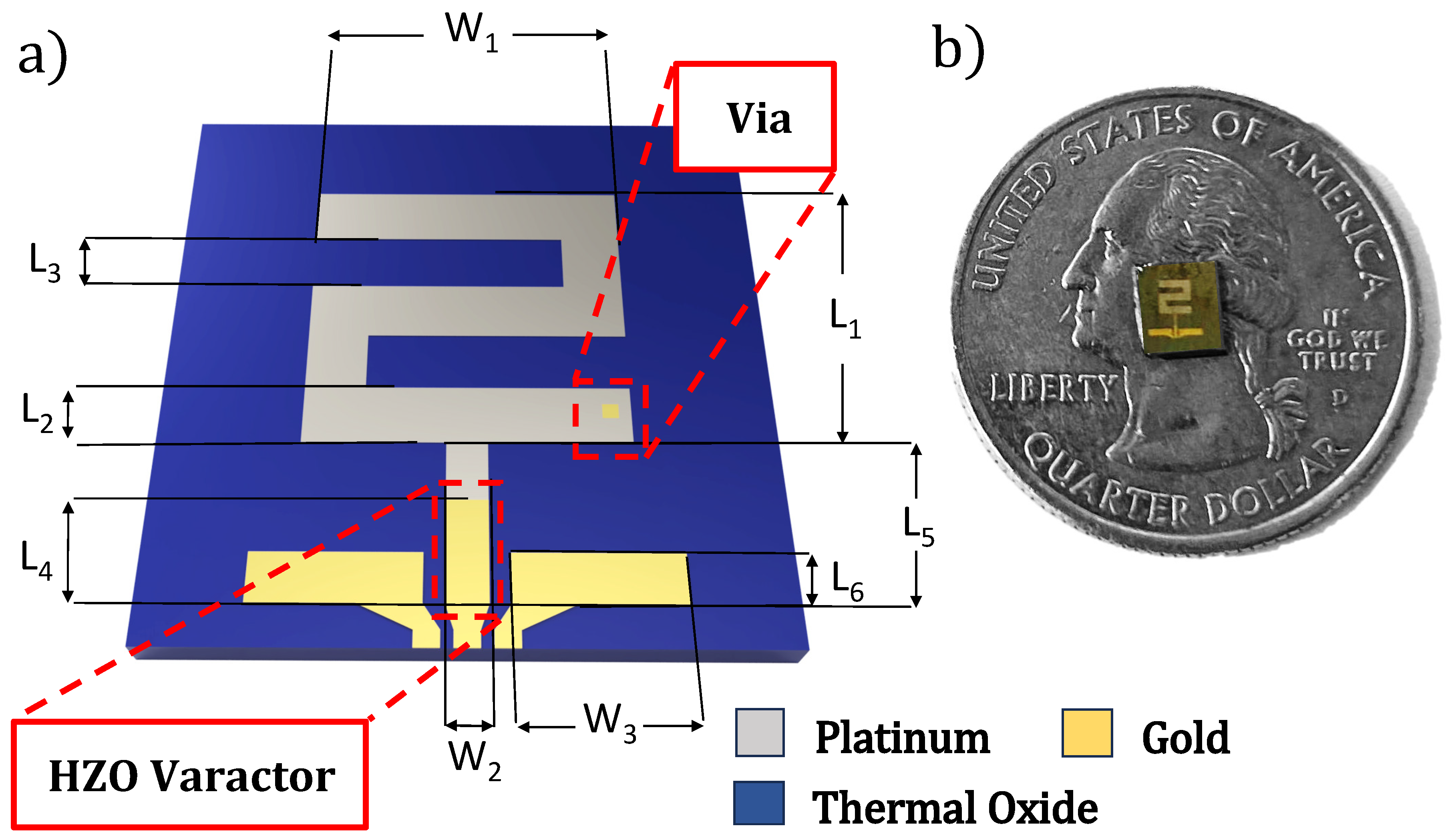
Figure 2.
a) Experimental ferroelectric polarization vs. applied voltage (PV) loop of the deposited HZO film. b) Experimental dielectric permittivity () vs. applied voltage curve extracted from the varactor. The reported device exhibits a Tuning Range (TR) of 28% between the dielectric permittivity at its coercive voltage (, 44.9) and at its maximum tunability (, 32.3). Both the PV loop and the CV curve were measured at 5 kHz with a triangular waveform.
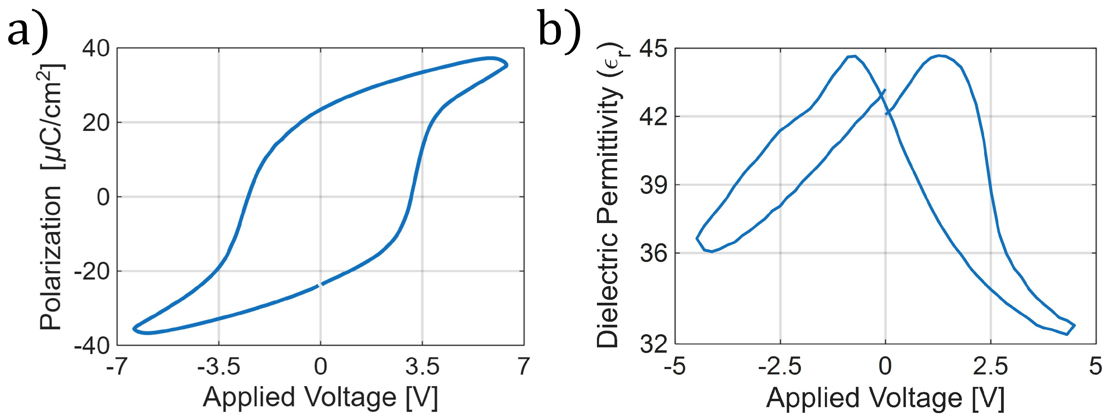
Figure 3.
Fabrication process and 5) cross-section of the proposed on-chip programmable antenna.
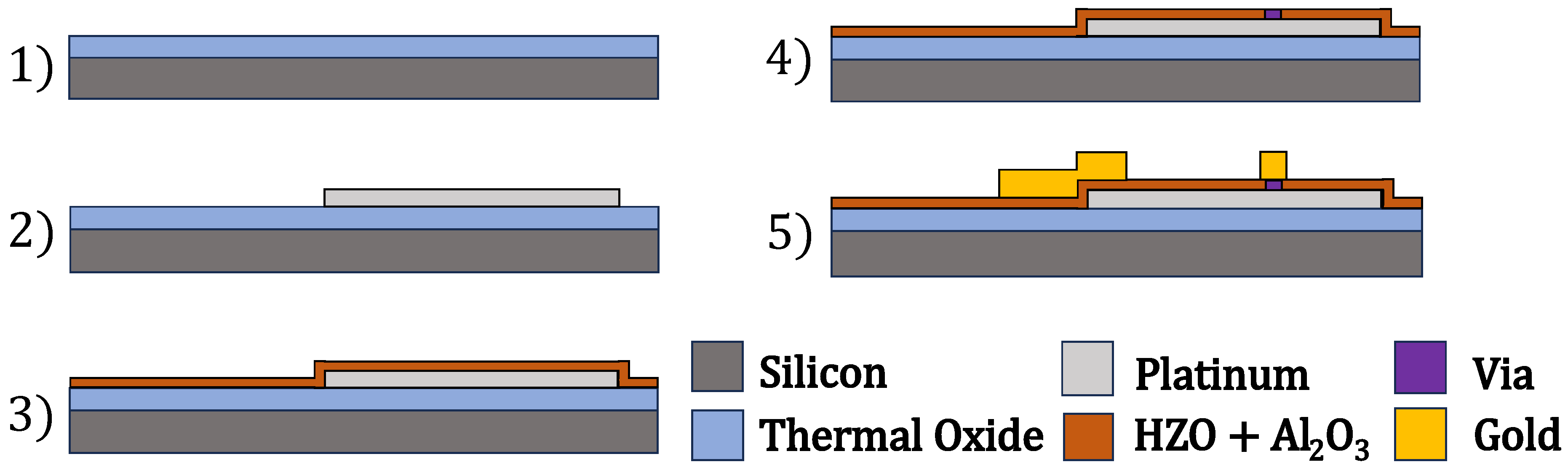
Figure 4.
SEM picture of the meander-line antenna, with emphasis on the monolithically-integrated HZO varactor structure along the microstrip line (left) and on the via structure (right).
Figure 4.
SEM picture of the meander-line antenna, with emphasis on the monolithically-integrated HZO varactor structure along the microstrip line (left) and on the via structure (right).
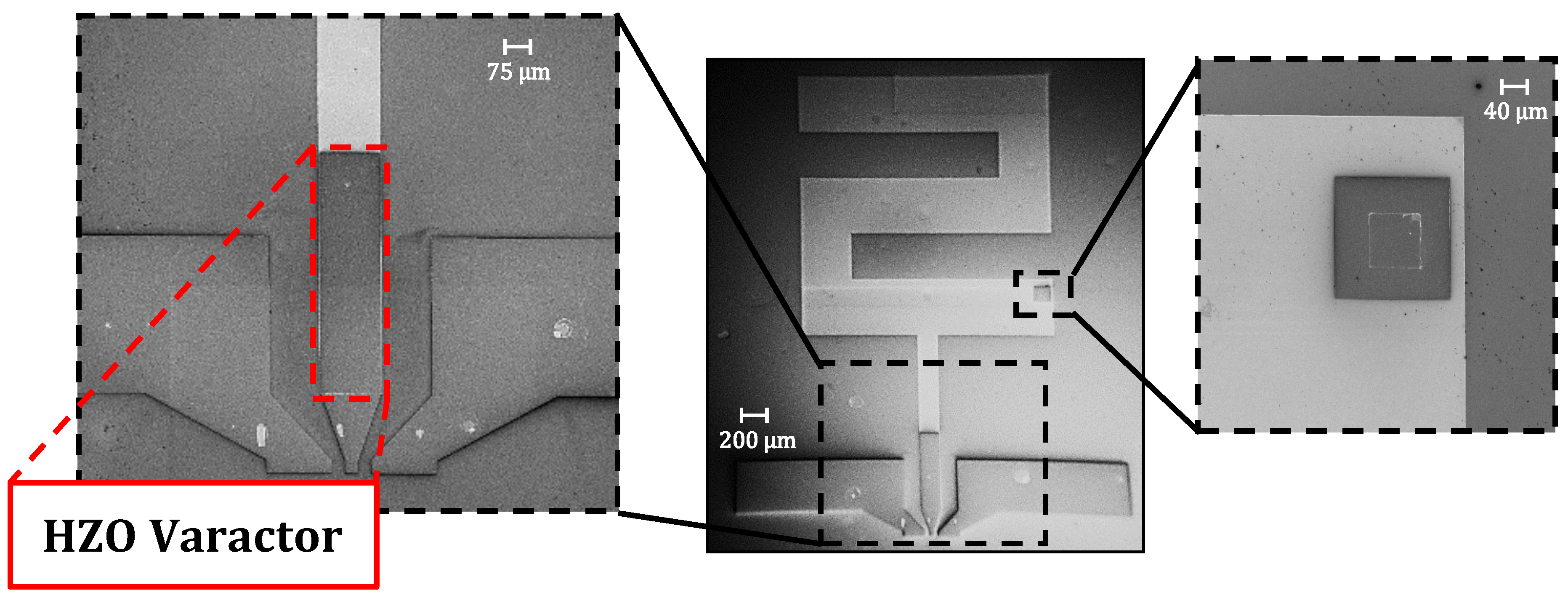
Figure 5.
Ferroelectrically-induced hysteresis loop of the antenna’s resonance frequency in response to the applied programming voltage. Point A denotes the maximum resonance frequency (8.78 GHz) obtained when applying a programming voltage of 3 V. Point B marks the minimum resonance frequency (8.399 GHz) observed with a programming voltage of -3.5 V. The inset reports the applied voltage profile during the partial polarization experiment between -5 V and 5 V.
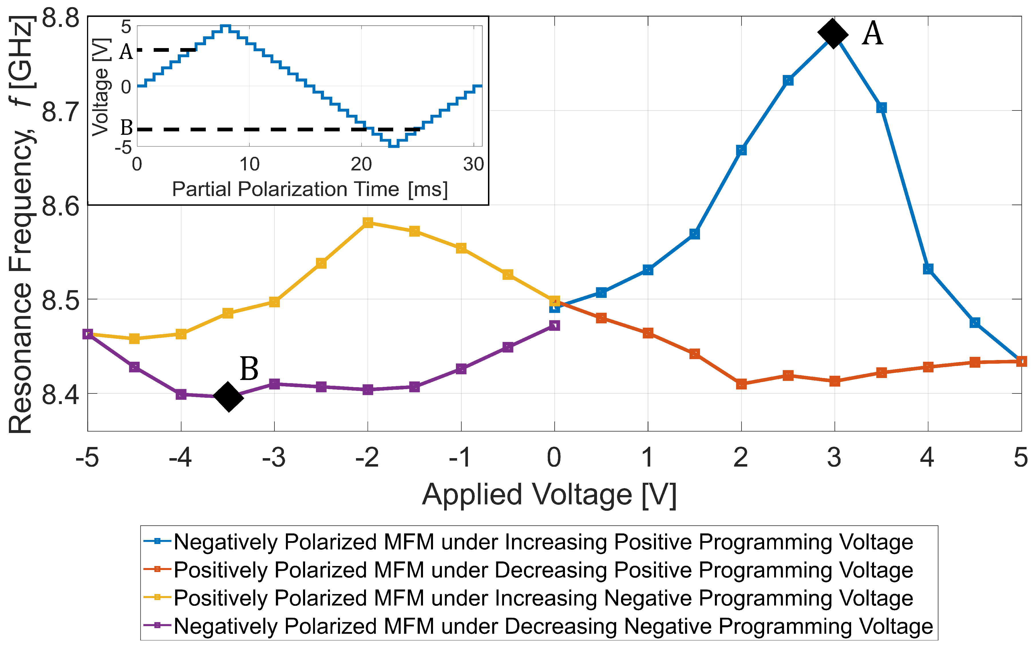
Figure 7.
Measured (continuous lines) and simulated (dashed lines) gain vs. frequency trends for points A (3 V) and B (-3.5 V). The inset on the bottom left shows the measurement setup used to extract the gain vs. frequency profile and the radiation diagrams.
Figure 7.
Measured (continuous lines) and simulated (dashed lines) gain vs. frequency trends for points A (3 V) and B (-3.5 V). The inset on the bottom left shows the measurement setup used to extract the gain vs. frequency profile and the radiation diagrams.
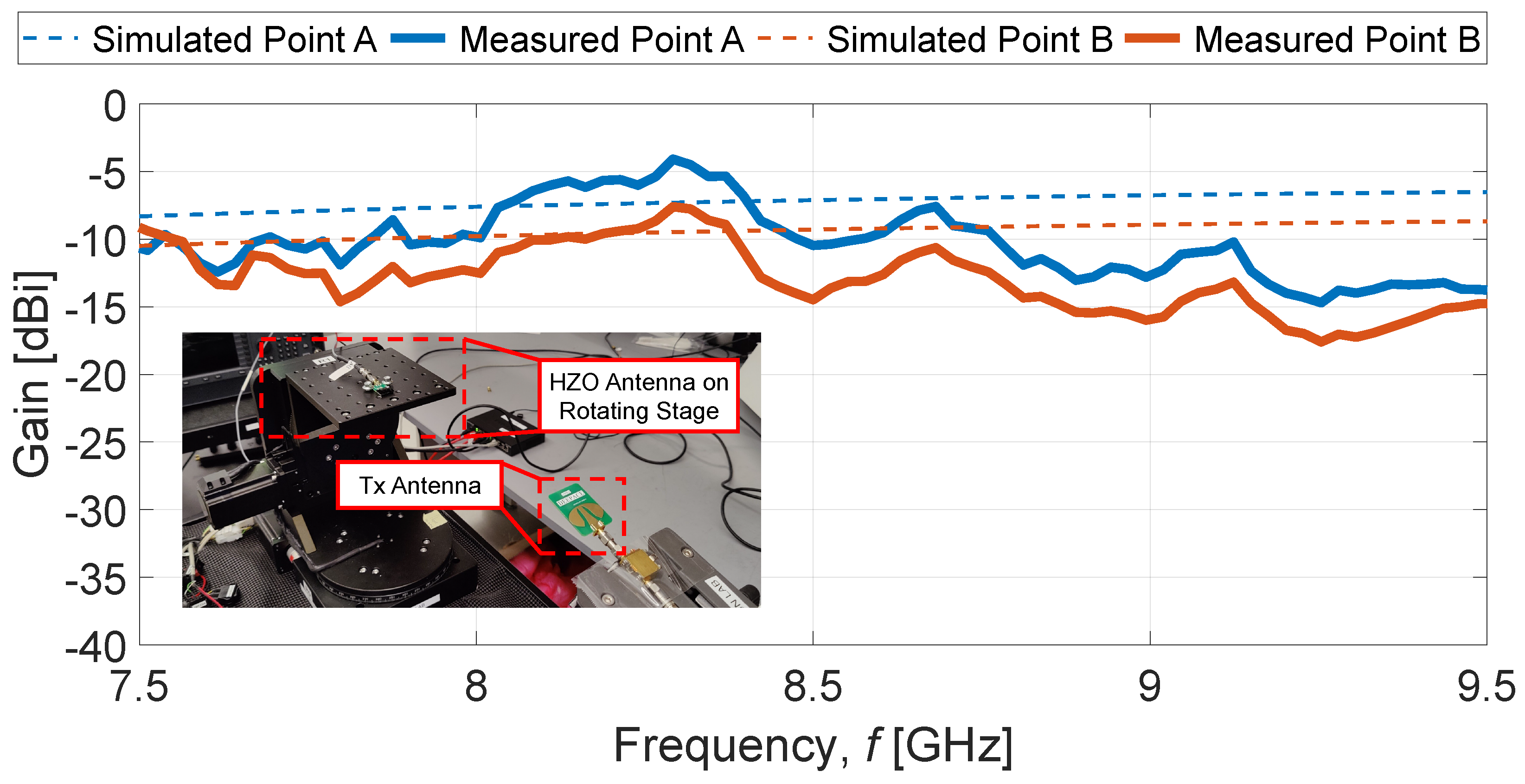
Figure 8.
Normalized measured (continuous lines) and simulated (dashed lines) radiation diagrams showing the antenna gain in dB in the E-plane (a) and H-plane (b) for the two polarization states of the SHF mode.
Figure 8.
Normalized measured (continuous lines) and simulated (dashed lines) radiation diagrams showing the antenna gain in dB in the E-plane (a) and H-plane (b) for the two polarization states of the SHF mode.
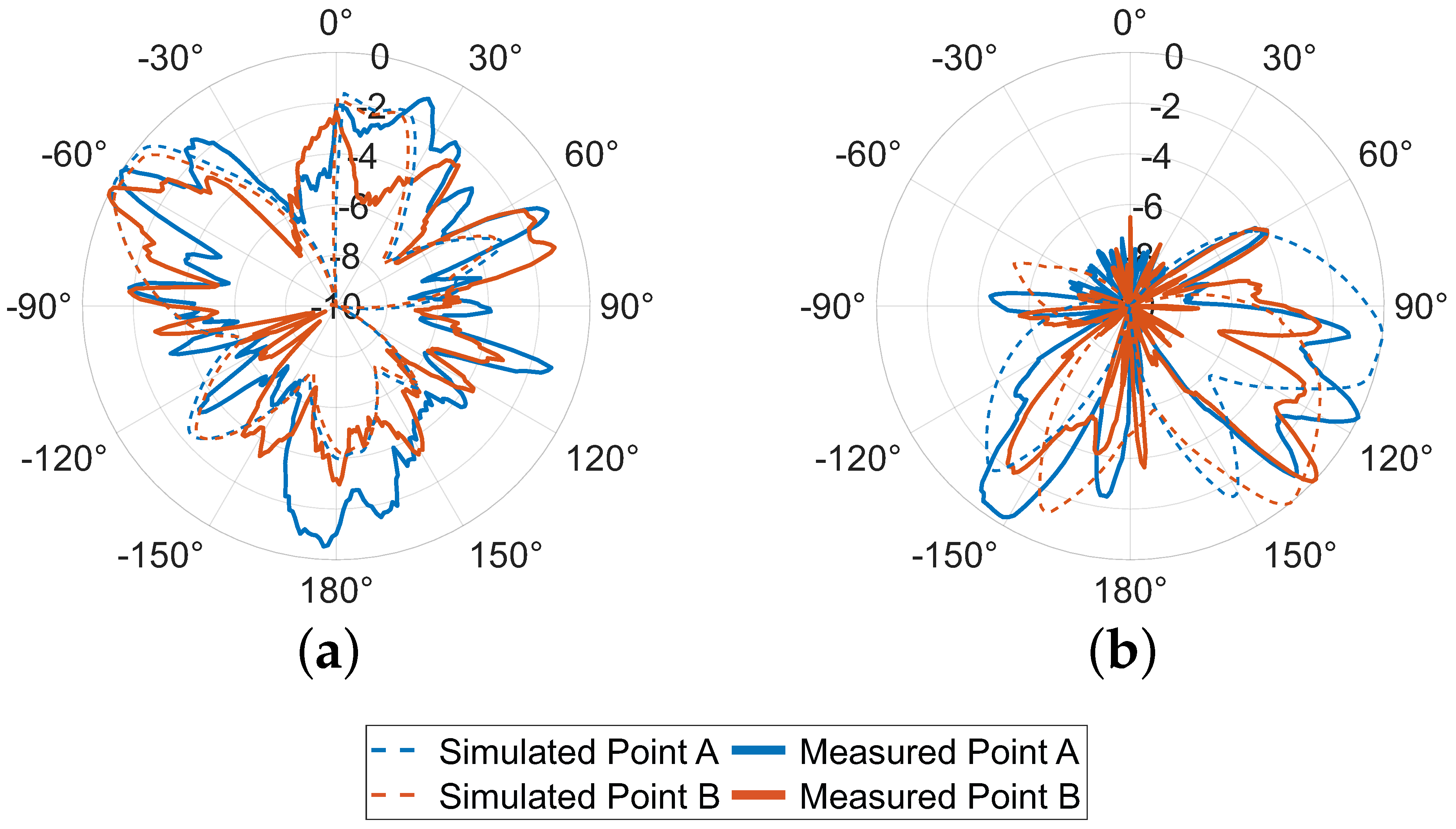
Figure 9.
Ferroelectrically-induced hysteresis loop of the EHF mode’s resonance frequency in response to the applied programming voltage. Point A denotes the maximum resonance frequency (37.957 GHz) obtained when applying a programming voltage of 3 V. Point B marks the minimum resonance frequency (34.938 GHz) observed with a programming voltage of -3 V. The inset reports the applied voltage profile for the partial polarization experiment between -5 V and 5 V.
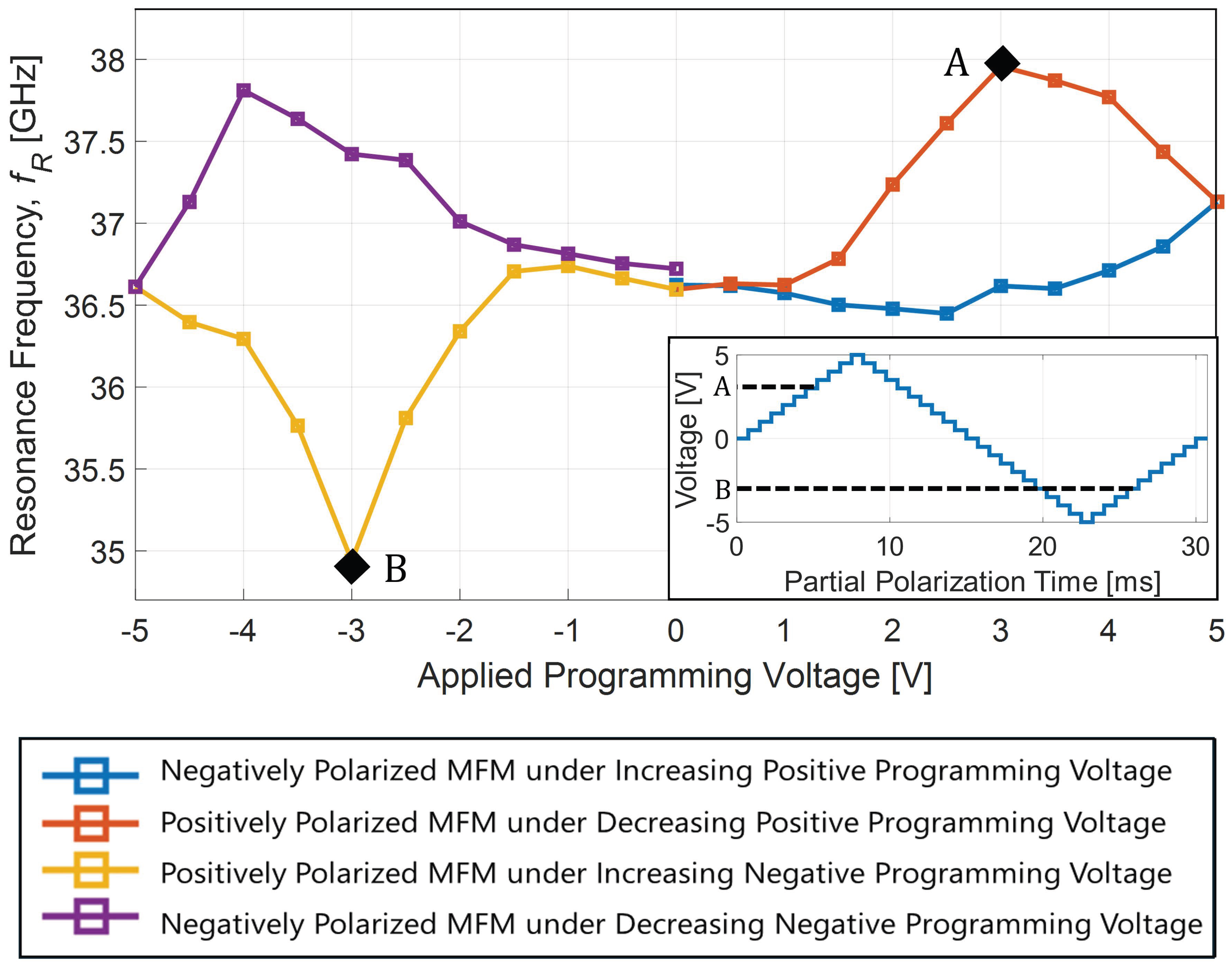
Figure 10.
Measured and simulated parameters for point A (3 V) and point B (-3 V) of the EHF mode.
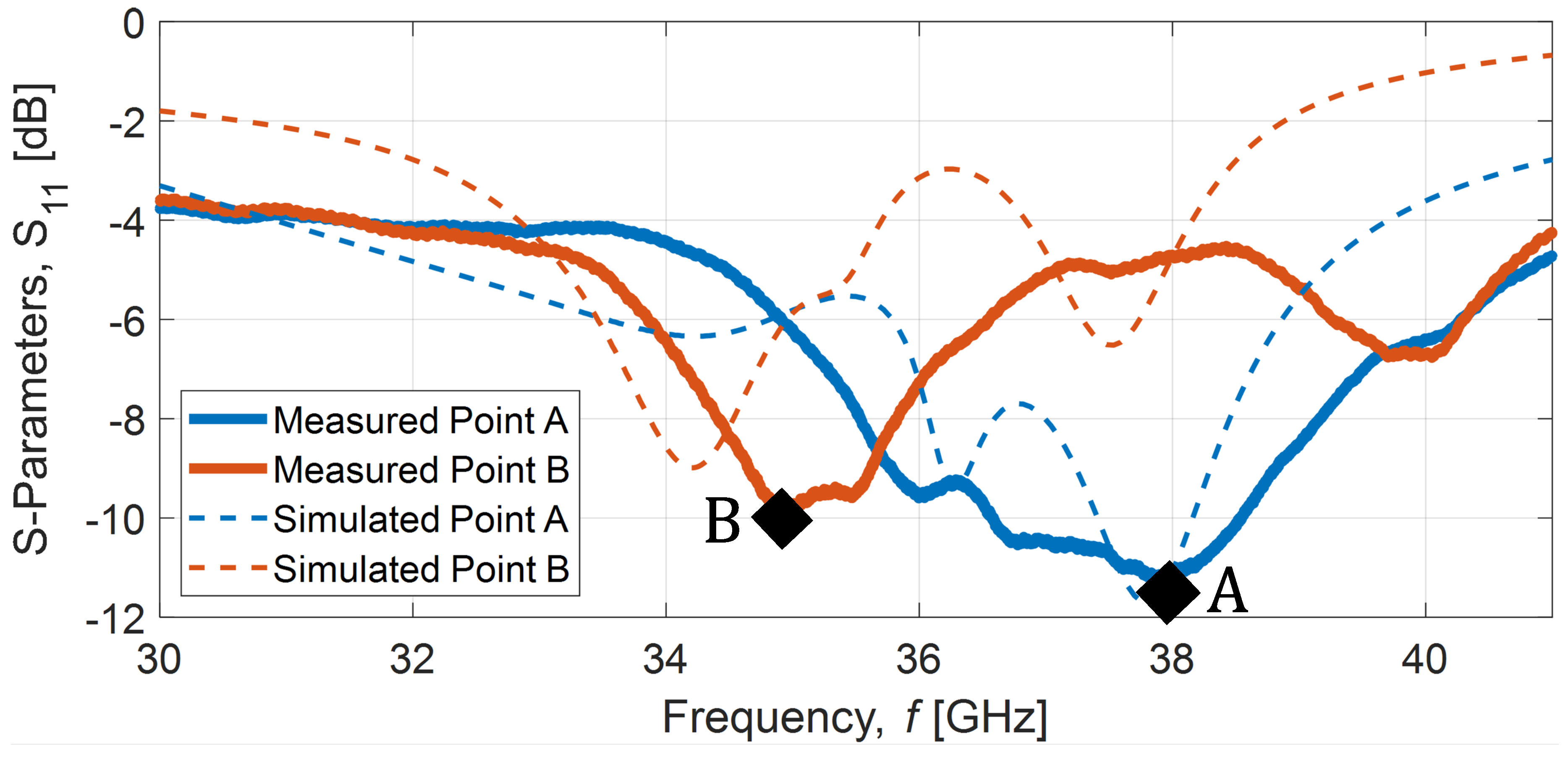
Figure 11.
Measured (continuous lines) and simulated (dashed lines) gain vs. frequency trends for points A (3 V) and B (-3 V) of the EHF mode.
Figure 11.
Measured (continuous lines) and simulated (dashed lines) gain vs. frequency trends for points A (3 V) and B (-3 V) of the EHF mode.
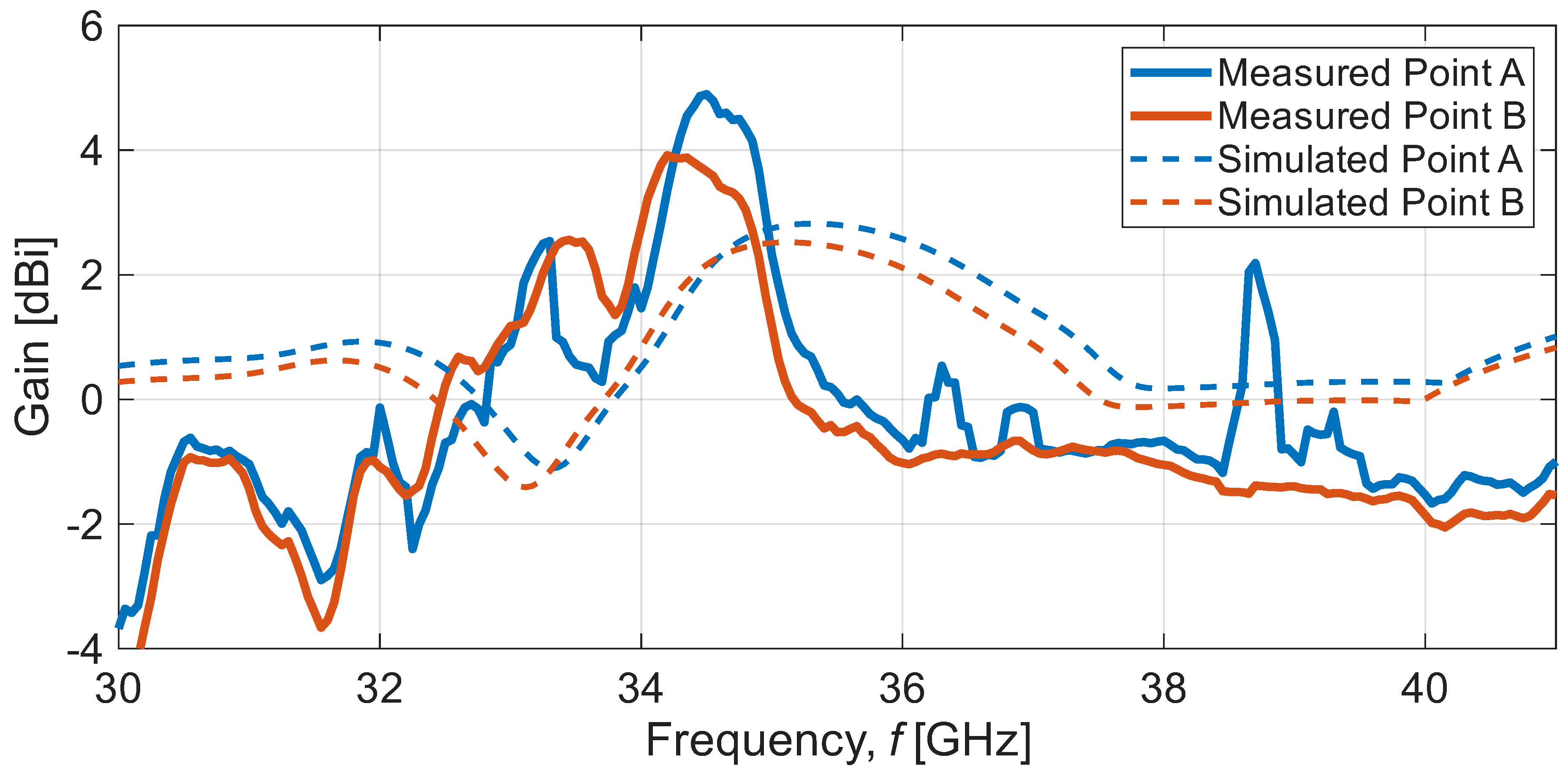
Figure 12.
Normalized measured (continuous lines) and simulated (dashed lines) radiation diagrams showing the antenna gain in the E-plane (a) and H-plane (b) for the two polarization states of the EHF mode.
Figure 12.
Normalized measured (continuous lines) and simulated (dashed lines) radiation diagrams showing the antenna gain in the E-plane (a) and H-plane (b) for the two polarization states of the EHF mode.
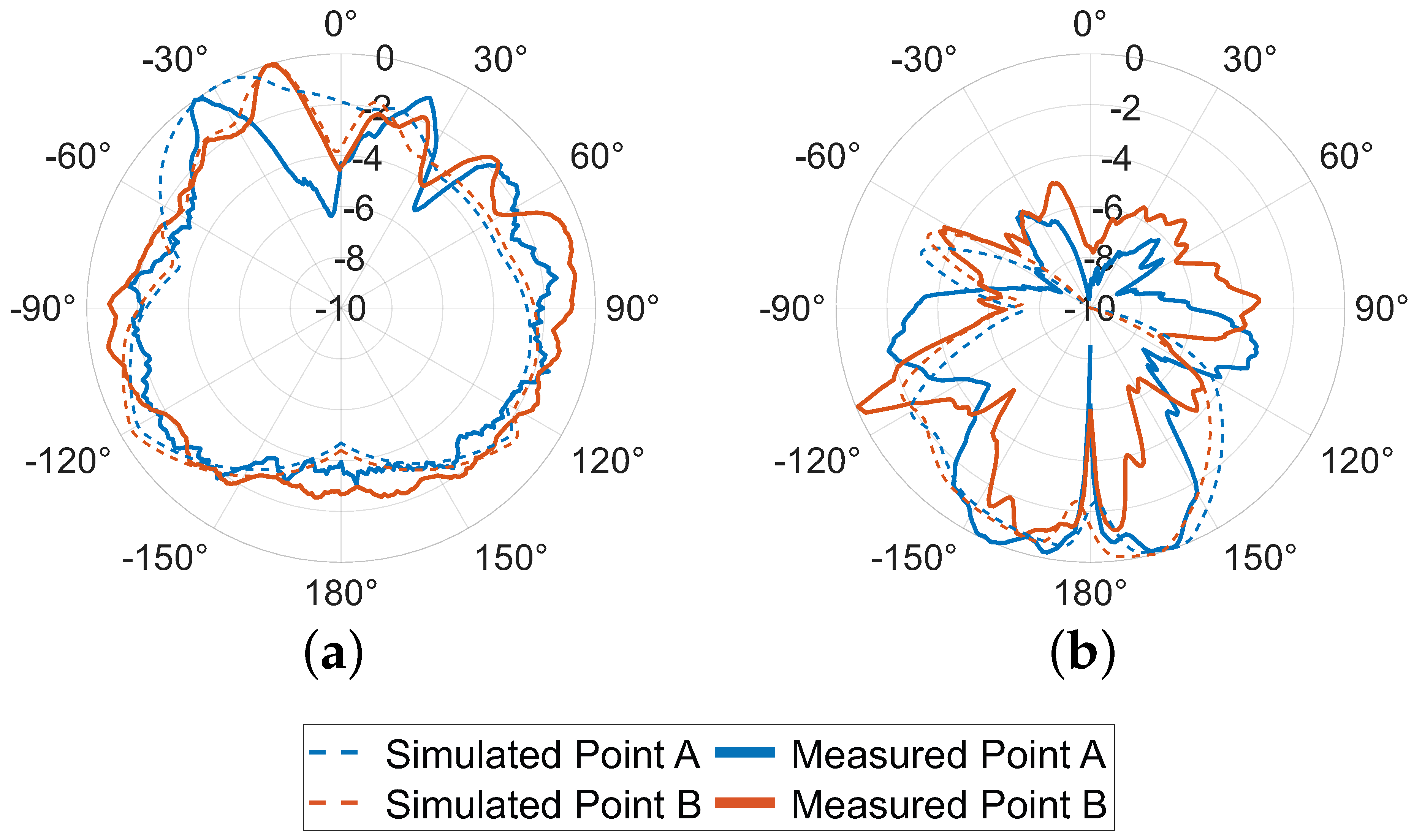

Table 1.
In-Plane Dimensions of the Ferroelectrically-Programmable Meander-Line Antenna.
| Symbol | |||||||||
| Length [m] | 1680 | 1500 | 460 | 300 | 460 | 115 | 1080 | 300 | 950 |
Table 2.
Comparison Between Different Ferroelectric-Based Thin Film Reconfigurable Antennas
| Work | Frequency Shift† | Material | Area | CMOS Compatible | Maximum Gain | Voltage | UWB Mode | Fractional Frequency Change | Non-Volatile Programmability |
| [16] | 17–17.3 GHz | KTN | 100 mm2 | No | 6.7 dBi | 0–150 V | No | 1.7% | No |
| [17] | 15.2–16 GHz | KNN | 16 mm2 | No | -2 dBi | 0–150 V | No | 4.6% | No |
| [42] | 0.6–0.75 GHz | BST | 645 mm2 | No | †† | 0–30 V | No | 14.5% | No |
| [43]††† | 28–30.7 GHz | BST | 1.75 mm2 | No | -7.5 dBi | 0–100 V | No | 16.7% | No |
| [21] | 9–9.2 GHz | HZO, Metamaterial, Resonator | 139.7 mm2 | Yes | 4 dBi | ±2 V | No | Not Provided, 2% Estimated | No |
| This work | 8.4–8.78 GHz | HZO | 6.5 mm2 | Yes | -4 dBi | ±5 V | Yes | 4.5% | Yes |
| This work | 34.9–37.9 GHz | HZO | 6.5 mm2 | Yes | 5 dBi | ±5 V | No | 8.3% | Yes |
†Measured resonance frequencies at the maximum frequency variation. ††Gain not provided, the measured efficiency is up to 1%. †††The results are only based on simulations, no physical device was built.
Disclaimer/Publisher’s Note: The statements, opinions and data contained in all publications are solely those of the individual author(s) and contributor(s) and not of MDPI and/or the editor(s). MDPI and/or the editor(s) disclaim responsibility for any injury to people or property resulting from any ideas, methods, instructions or products referred to in the content. |
© 2026 by the authors. Licensee MDPI, Basel, Switzerland. This article is an open access article distributed under the terms and conditions of the Creative Commons Attribution (CC BY) license (http://creativecommons.org/licenses/by/4.0/).
Copyright: This open access article is published under a Creative Commons CC BY 4.0 license, which permit the free download, distribution, and reuse, provided that the author and preprint are cited in any reuse.


