Submitted:
30 December 2025
Posted:
30 December 2025
You are already at the latest version
Abstract
Through theoretical analysis, we demonstrate that a capacitor modeled as a parallel combination of a resistance (R) and a capacitance (C), with a current–voltage characteristic I = I (E), exhibits a volatile negative capacitance effect when the condition I′(E) > I (E) is satisfied. In contrast, ordinary dielectric capacitors satisfy I′(E) < I (E), resulting in the accumulation of free charge on the plates and a positive capacitance. When the capacitive component becomes negligible and only resistance remains, I′(E) = I (E) and which corresponds to Ohm’s law. We fabricated two-electrode structures with nanometer-scale spacing using multi-walled carbon nanotubes (MWCNTs) and Si crystals as electrode materials. Experimental measurements confirmed the presence of negative capacitance, in agreement with theoretical predictions. Unlike ferroelectric-origin negative capacitance, this mechanism arises from the I − V characteristics between electrodes. We further show that this negative capacitance can be equivalently represented as an inductance in a circuit, enabling its use as a two-dimensional inductor without electromagnetic interaction. Circuit-level integration and broader applications are anticipated.
Keywords:
two-dimensional inductor
; current–voltage characteristic
; electromagnetic interaction
; negative capacitance
; integrated circuits
1. Introduction
Classical circuits are composed of passive elements: resistors , capacitors , and inductors . The emergence of semiconductor devices and novel materials has introduced active elements such as diodes and transistors and devices with material-dependent functionalities, significantly transforming circuit design, operating principles, and application domains [1,2,3,4,5]. In recent years, unconventional passive elements such as negative resistance and negative capacitance have been reported [6,7,8,9,10]. Studies of nonlinear current–voltage () characteristics in vacuum tubes and gas discharge tubes revealed phenomena in which current decreases as voltage increases; this observation formed the basis of negative differential resistance. The tunnel diode invented by R. Esaki et al. [11,12], exhibits a pronounced negative-resistance region, attracted considerable attention as a practical device, spurring extensive research into its mechanisms and applications. As discussed below, negative resistance plays a critical role in the emergence of negative capacitance.
Recently, fully two-dimensional inductors that operate without coils or magnetic fields have been proposed [13,14]. Because they are based on principles fundamentally different from those of conventional magnetically coupled inductors, they offer significant potential for integration and miniaturization. Planar implementations enable on-chip inductors and support the downsizing of high-frequency and resonant circuits. In the GHz bands used for RF communications and 5G/6G devices, conventional coil-type inductors face limitations in size and energy loss; planar inductors rendering planar inductors a promising alternative. In coil-free power circuits, realizing inductance without wound coils for DC–DC converters and output filters could enable thinner, lighter power-supply designs.
This paper investigates physical origin, quantitative characteristics, device realization, and challenges. We further extend the concept to propose a method for realizing two-dimensional inductors and present both experimental and theoretical validation.
2. Theory and Practice of Negative Capacitance
2.1. Definition and Background
The term “negative capacitance” has gained prominence in recent years. In 1986, Jonscher discussed its physical origin of negative capacitance, defining it as a phenomenon in which the current temporarily decreases in response to a voltage step in the time domain [15]. Since then, negative-capacitance effects in ferroelectric materials have attracted attention, and since the 2010s, research into their application to transistor gate control has progressed rapidly. Research groups at institutions such as Stanford and Bell Labs have designed and demonstrated Negative Capacitance Field-Effect Transistors (NC-FETs), which are considered promising for low-power electronics [16,17].
Traditionally, negative capacitance is attributed to intrinsic ferroelectric properties of a dielectric layer between electrodes, where interplay between ferroelectric and dielectric responses can yield an effective capacitance that is positive or negative [9,16,18,19]. Since a capacitor is inherently non-polar, “negative capacitance” is strictly a phenomenological description of a reduction or sign reversal of effective capacitance.
In contrast, this work reports negative capacitance that does not originate from ferroelectric effects but from a circuit phenomenon produced by controlling the capacitor’s I–V characteristic. Specifically, when the current lags the voltage in phase, negative capacitance appears; because no positive free charge remains on the plates when power is turned off, we refer to this as volatile negative capacitance.
2.2. Ferroelectric-Origin Negative Capacitance
When a ferroelectric material is employed as the dielectric layer, its free-energy profile can lead to responses that differ significantly from those of conventional capacitors. The free energy of a ferroelectric typically exhibits a bistable double-well shape as a function of polarization, with a region of negative curvature between the wells. In that negative-curvature region, the polarization response to an applied electric field --i.e., the differential capacitance-- can become negative. This phenomenon constitutes the physical origin of ferroelectric negative capacitance [9,16,18,19,20].
Such negative capacitance is thermodynamically unstable for a single ferroelectric layer and is usually stabilized by connecting it in series with a paraelectric or dielectric layer. In a series structure, when the ferroelectric layer passes through the negative-capacitance region, the overall voltage response becomes nonlinear, and an internal voltage amplification effect can be obtained. This effect is of interest for reducing the subthreshold slope (SS) of transistors below 60 mV/dec and is being pursued for NC-FET applications [21,22].
Domain structure, interface states, film thickness, and crystallinity strongly influence negative-capacitance manifestation; precise control of these factors is key to stable operation. HfO2-based ferroelectrics are promising due to CMOS compatibility [18,23,24,25,26].
2.2.1. Basic Theory
Negative capacitance arises when the curvature of the free energy with respect to small fluctuations in polarization is negative. Let the free-energy density be denoted as F(P) and the electric field E be the derivative of free energy with respect to polarization [27]:
For a capacitor, the terminal voltage is given by where is thickness, and the terminal charge density corresponds to . The differential capacitance is
Differentiating with respect to yields
Thus, the differential capacitance becomes.
Therefore, if , then and the differential capacitance can be negative. In thermodynamic equilibrium, the free energy must be minimized, and local stability requires . Regions with negative curvature are unstable and the system tends to transition to a nearby stable state via polarization switching, domain formation, or other relaxation.
Experimentally observed negative capacitance often stems from transient responses rather than static equilibrium. Delayed processes associated with domain formation or polarization reversal (domain-wall motion, relaxation times, interface decay) can make the current response to a step voltage temporarily reverse [27].
2.2.2. Applications and Challenges
Numerous research groups have explored ferroelectric negative capacitance for its potential in voltage amplification and low-power electronics. Datta’s group has conducted quantum-theoretical analyses and TCAD simulations to elucidate the underlying mechanisms [28]; Pop’s group has focused on HfO₂ thin films and interface engineering [29]. Although negative capacitance holds promise for low-voltage transistors and memory devices, several challenges remain, including the suppression of hysteresis, precise control of interfacial properties, and the ability to distinguish between volatile and nonvolatile behavior depending on the application context. [28].
2.3. Negative Capacitance Originating from Current Voltage Characteristics
In ferroelectric capacitors, the application of voltage can alter the permittivity and reduce the effective capacitance due to intrinsic material nonlinearity; this behavior can resemble negative capacitance when the voltage–current response is nonlinear. However, aside from specific ferroelectrics such as HfO₂, this effect is minimal in conventional dielectrics and is rarely observed. A key feature of such systems is the accumulation of nonvolatile free charge on both electrodes when the capacitor is charged.
In this study, we report the realization of negative capacitance by deliberately introducing nonlinear characteristics between electrodes. Specifically, we propose inducing negative capacitance by driving field-emission currents at two electrode interfaces and tailoring the response accordingly [13,14]. Field-emission current from a material surface into vacuum follows the Fowler–Nordheim relation () [30], which deviates from Ohm’s law. In our recent work, we observed the manifestation of negative capacitance in a capacitor formed by facing two electrode materials across a vacuum gap. Unlike ferroelectric negative capacitance, this form is volatile: when power is removed, the free charge on the plates dissipates [13,14].
2.3.1. Basic Theory
A conventional capacitor can be modeled as a parallel circuit consisting of a capacitance C and a leakage-related resistance R. When a constant current source is applied across the electrodes, a voltage V develops between them. Let currents through the capacitor C and resistor R be denoted as and , respectively. Then [13]
The charge accumulated on the capacitor plates at time is
Assuming is constant and is a function of , the capacitance becomes.
From this expression, the sign of capacitance () can be determined. Assuming is nonnegative, three operating regimes are identified:
In the first case the relative change in resistance exceeds that of voltage. Rewriting the condition,
This implies that (R/V) increases with V, the reciprocal current decreases, and charge accumulation on the plates, resulting in positive capacitance.
High-resistance dielectric capacitors often exhibit conduction mechanisms such as polarization current [31], leakage current [32], thermally activated conduction (e.g., Poole–Frenkel or trap-limited) [32], space-charge-limited conduction (SCLC) [34,35,36], and tunneling conduction (e.g., Fowler–Nordheim) [30]. For many dielectrics, the SCLC follows a power-law dependence:
with derivative:
Figure 1 illustrates this behavior for (), showing that of the function and its derivative on the electric field strength. The figure reveals regions where . In the SCLC-dominated region, , resulting in a positive, nonvolatile capacitance. In the limit , the dielectric approaches an ideal positive capacitor.
In the regime 2 , integrating gives with constant, hence
so is proportional to and Ohm’s law holds. In the case the capacitance does not contribute and the equivalent circuit is purely resistive.
and its derivative.
In the regime 3 , the relative change of is smaller than that of . The relative change of is
Thus : increasing voltage increases the current through , meaning decreases. If tunneling current dominates between electrodes.
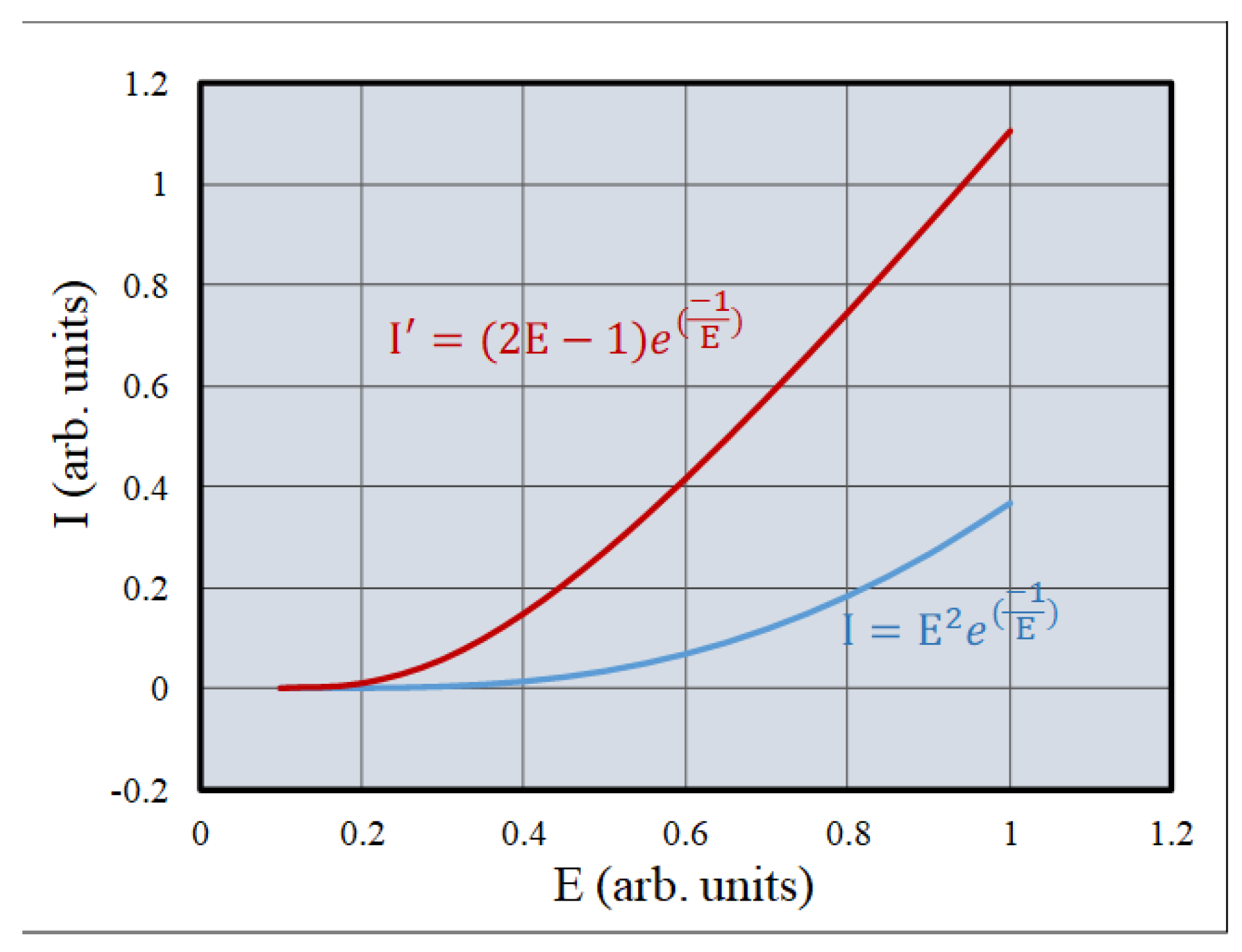
As an example, consider tunneling (field-emission) current [30]:
Its derivative is
Figure 2 shows the dependence of the function and its derivative on the electric field strength. Using the expressions in Eqs. (16) and (17) with , one finds regions where . Introducing tunneling current between electrodes can therefore yield volatile negative capacitance. This offers a pathway toward ideal negative-capacitance devices, though practical realization requires careful material selection and interface control.
and its derivative on the electric field strength.
2.3.2. Applications and Outlook
Ferroelectric-based negative capacitance is applicable to low-power electronic devices but is often constrained by high internal resistance. In contrast, negative capacitance arising from nonlinear current–voltage () characteristics enables the deliberate engineering of internal resistance and, in extreme cases, implementation using only two metallic electrodes. This flexibility broadens the applicability of negative-capacitance devices across a wide power range. Moreover, this type of negative capacitance can emulate inductive behavior, enabling the realization of coil-free two-dimensional inductors. While it may not fully replace conventional electromagnetic inductors, it offers new functional possibilities.
3. Two-Dimensional Inductor Without Electromagnetic Interaction
3.1. Basic Theory
Conventional inductors include three-dimensional windings with magnetic cores [37,38] and near-two-dimensional thin-film spiral coils [39]. A truly two-dimensional inductor could eliminate constraints such as height, volume, and dependence on magnetic cores while thereby enabling on-chip integration and contributing to miniaturization.
The impedance of a series circuit consisting of resistance (), inductance (), and capacitance () is given by
If () is negative, the effect of negative capacitance can be incorporated into the inductive term. The resulting effective inductance becomes.
Although the contribution of the term diminishes at high frequencies as , in the low-frequency region the effective inductance corresponds to . Under appropriate conditions, the circuit elements () and () can be functionally interchanged, and transformations such as and can be expected. Physically, if tunneling current is introduced into an ordinary capacitor that blocks current, the resulting phase relationship between current and voltage can resemble that of an inductor, providing a theoretical basis for converting negative capacitance into inductive behavior.
3.2. Experimental Realization
Our group is developing a fully two-dimensional inductor designed to avoid electromagnetic interaction [13,14]. Related publications and patents to date are limited to our work. This approach cannot replicate all functions of conventional electromagnetic inductors; it cannot store magnetic energy or provide energy isolation. Typical roles of conventional inductors include magnetic energy storage [40], filtering and noise suppression [32], tuning and frequency selection [41], impedance transformation and matching [41], energy isolation [40], and control of time constants and transient responses [42].
First, we examined inductors using compressed pellets of multi-walled carbon nanotube (MWCNT) powder [13]. MWCNT pellets form a transport system that combines one-dimensional quantum conduction within tubes and complex inter-tube contacts, tunneling junctions, and disorder. By adjusting pellet compression, tunneling conduction can be made dominant.
Using a 5 mm diameter, ~0.5 mm thick MWCNT pellet, we fabricated an electrode/MWCNT/interface/MWCNT/electrode structure [14]. This structure allows tunneling currents inside MWCNTs and at MWCNT/MWCNT contact interfaces. We measured the samples using an impedance analyzer and analyzed frequency dependence, AC amplitude dependence, and DC bias dependence of inductance. By adjusting contact distance between two pellets to modulate the contact area, we demonstrated control over the tunneling conduction component. Currents through MWCNT/MWCNT interfaces can be decomposed into conductive, polarization, and tunneling components; controlling the tunneling component clarified its role in inductance generation.
Below 1 kHz, inductance decreased monotonically with increasing frequency, reaching a maximum of approximately 0.3 mH at the lowest frequency. This frequency dependence is consistent with the term in . We also observed that increasing AC amplitude led to an increase in inductance.
Next, we fabricated an electrode/Si/interface/Si/electrode structure using p-type Si (100) wafers of area , thickness , and resistivity of . In this structure tunneling current occurs only at the Si contact interface, allowing clear separation of interface and bulk tunneling contributions. We applied undulating surface processing to the Si wafers and selected pairs so that contacts became point or line contacts when two wafers face each other. Theoretical calculations indicate that tunneling current contribution is larger for point contacts than for line contacts. Under these conditions we investigated the contribution of tunneling current to inductance.
Inductance analysis confirmed the presence of two-dimensional inductance in the electrode/Si/interface/Si/electrode structure. We found that inductance can be controlled by frequency, AC amplitude, and DC bias. From these results we conclude that two-dimensional inductance is realized when tunneling current flows only at the electrode interface.
3.3. Challenges and Outlook
We utilized the distinctive current–voltage () characteristics of field-emission current () from material surfaces to achieve the functional transformation between inductance and negative capacitance . Similar behavior is expected in devices exhibiting negative differential resistance, such as Esaki diodes, resonant-tunneling diodes, Gunn diodes, high-frequency discharge devices, unijunction transistors, and certain switching devices.
Advancing the research and development of two- and three-dimensional negative-capacitance and inductor elements may open new scientific and technological frontiers. These include novel passive components for integrated circuits, miniaturized RF systems, and unconventional energy-handling devices. However, challenges remain in terms of stability, reproducibility, and integration with existing semiconductor technologies. Further investigation into material selection, interface engineering, and circuit-level modeling will be essential for practical implementation.
4. Conclusions
By introducing a nonlinear current–voltage () characteristic between two electrodes, we have demonstrated the realization of volatile negative capacitance and two-dimensional inductance. Theoretical analysis and device characterization suggest that these elements can function as standalone negative-capacitance components or inductors and can be integrated into on-chip systems.
A capacitor modeled as a parallel combination of resistance () and capacitance () exhibits three distinct operating regimes when and depend on the voltage : a positive-capacitance regime in which the relative change of resistance dominates ; an Ohmic regime where the relative changes are equal (); and a negative-capacitance regime in which the relative change of capacitance dominates . When resistance dominates (), the system behaves as a conventional capacitor determined by permittivity; when capacitance dominates (), negative capacitance emerges, governed by the nonlinear characteristic. Thus, low-resistance conditions favor the formation of negative capacitance.
Negative capacitance can be interpreted as an effective inductance in circuit theory; with the equivalent inductance given by . Unlike ordinary dielectric capacitors (), the equivalent inductance depends on both frequency and on the magnitude of the negative capacitance. The inductance is more pronounced at low frequencies and decreases rapidly with increasing frequency, following the dependence.
The frequency response of a two-dimensional inductor is determined by the circuit time constant, specifically the product of resistance and negative capacitance. If can be made sufficiently small, high-frequency operation becomes feasible. For example, with and , operation near 1 MHz is achievable.
Because the two-dimensional inductance depends on bias and amplitude, it is necessary to establish a quiescent operating point—analogous to transistor biasing—to ensure stable circuit performance.
A fully two-dimensional inductor is a novel device that requires no coils or magnetic fields and holds promises for applications in integrated circuits, high-frequency communication systems, quantum technologies, and beyond.
Author Contributions
Conceptualization, Y.S.; methodology, S.K.; software, Y.S. and S.K.; validation, Y.S. and S.K.; formal analysis, Y.S. and S.K.; investigation, Y.S.; resources, Y.S.; data curation, Y.S.; writing—original draft preparation, Y.S. and S.K.; writing—review and editing, Y.S. and S.K.; visualization, Y.S.; supervision, Y.S.; project administration, Y.S.; funding acquisition, Y.S. All authors have read and agreed to the published version of the manuscript.
Conflicts of Interest
The authors declare no conflict of interest. .
References
- Liu, M.; Peng, L.-M. Emerging materials and transistors for integrated circuits. Natl. Sci. Rev. 2024, 11, nwae040. [Google Scholar] [CrossRef]
- Tolasa, D. G. The physics of semiconductor devices: Principles, applications, and innovations. Am. J. Phys. Appl. 2025, 13, 13–22. [Google Scholar] [CrossRef]
- Xie, J.; Zhou, Y.; Faizan, M.; Li, Z.; Li, T.; Fu, Y.; Wang, X.; Zhang, L. Designing semiconductor materials and devices in the post-Moore era by tackling computational challenges with data-driven strategies. Nat. Comput. Sci. 2024, 4, 123–135. [Google Scholar] [CrossRef]
- IEEE Electron Devices Society. Future materials for beyond Si integrated circuits: A perspective. IEEE Xplore 2024. Available online: https://ieeexplore.ieee.org/document/10752743.
- Zhang, Y.; Chen, W. Physics-based modeling and simulation of semiconductor devices for circuit and system design. Discov. Electron. 2024, Springer. Available online: https://link.springer.com/collections/gidefgchbj.
- Qin, Y.; Li, J. Negative capacitance in ferroelectric heterostructures. Phys. Rev. B 2024, 110, 134101. [Google Scholar] [CrossRef]
- Li, B.; Zhang, X.; Zhu, D.; Yang, H.; Wang, X.; Jiang, J.; Di, Y.; Zhang, L.; Wu, J.; Yin, Z. Unveiling negative capacitance in ferroelectric heterostructures: A 3D energy landscape perspective. J. Appl. Phys. 2025, 137, 224101. [Google Scholar] [CrossRef]
- Huo, H.; Lü, W.; Zheng, X.; Wang, Y.; Zhao, S. Analysis and mitigation of negative differential resistance effects with hetero-gate dielectric layer in negative-capacitance field-effect transistors. J. Microelectron. Electron. Compon. Mater. 2024, 54, 65–73. [Google Scholar] [CrossRef]
- Salahuddin, S.; Datta, S. Use of negative capacitance to provide voltage amplification for low power nanoscale devices. Nano Lett. 2008, 8, 405–410. [Google Scholar] [CrossRef] [PubMed]
- Nature Electronics Editorial. Rethinking negative capacitance research. Nat. Electron. 2020, 3, 10–12. Available online: https://www.nature.com/articles/s41928-020-00483-8. [CrossRef]
- Esaki, L. New phenomenon in narrow germanium p–n junctions. Phys. Rev. 1958, 109, 603–604. [Google Scholar] [CrossRef]
- Tsu, R.; Esaki, L. Tunneling in a finite superlattice. Appl. Phys. Lett. 1973, 22, 562–564. [Google Scholar] [CrossRef]
- Sun, Y.; Yasunaga, H.; Shiraishi, M.; Sakai, H. Volatile capacitance of resistor with differential resistance. Appl. Phys. Lett. 2024, 125, 143501. [Google Scholar] [CrossRef]
- Yasunaga, H.; Yano, K.; Tanioka, Y.; Fujimoto, S.; Kanemitsu, S.; Sun, Y. Negative capacitance effect at interface between Si wafers with undulating surfaces. Crystals 2025, 15, 798. [Google Scholar] [CrossRef]
- Jonscher, A. K. The physical origin of negative capacitance. Nature 1986, 323, 673–676. [Google Scholar] [CrossRef]
- Khan, A. I.; Yeung, C. W.; Hu, C.; Salahuddin, S. Ferroelectric negative capacitance MOSFET: Capacitance tuning & antiferroelectric operation. IEDM Tech. Dig. 2011, 255–258. [Google Scholar] [CrossRef]
- Appleby, D. J. R.; Ponon, N. K.; Kwa, K. S. K.; Petrov, P. K.; Wang, T.; Alford, N. M.; O’Neill, A. G. Experimental observation of negative capacitance in ferroelectrics at room temperature. Nano Lett. 2014, 14, 3864–3868. [Google Scholar] [CrossRef]
- Hoffmann, M.; Pešić, M.; Slesazeck, S.; Schroeder, U.; Mikolajick, T. On the stabilization of ferroelectric negative capacitance in nanoscale devices. Nanoscale 2018, 10, 10891–10899. [Google Scholar] [CrossRef]
- Zubko, P.; Gariglio, S.; Gabay, M.; Ghosez, P.; Triscone, J.-M. Interface physics in complex oxide heterostructures. Annu. Rev. Condens. Matter Phys. 2011, 2, 141–165. [Google Scholar] [CrossRef]
- Catalan, G.; Jiménez, D.; Gruverman, A. Ferroelectrics: Negative capacitance detected. Nat. Mater. 2015, 14, 137–139. [Google Scholar] [CrossRef]
- Rusu, A.; Salvatore, G. A.; Jiménez, D.; Ionescu, A. M. Metal–ferroelectric–metal–oxide–semiconductor field effect transistor with sub-60 mV/dec subthreshold swing and internal voltage amplification. IEDM Tech. Dig. 2010, 395–398. [Google Scholar] [CrossRef]
- Jain, A.; Radhakrishna, U.; Wong, H.-S. P.; Saraswat, K. C. Analysis of capacitance–voltage characteristics of ferroelectric MOS capacitors. IEEE Trans. Electron Devices 2017, 64, 2905–2910. [Google Scholar] [CrossRef]
- Müller, J.; Böscke, T. S.; Schröder, U.; Mueller, S.; Bräuhaus, D.; Böttger, U.; Frey, L.; Mikolajick, T. Ferroelectricity in simple binary ZrO₂ and HfO₂. Nano Lett. 2012, 12, 4318–4323. [Google Scholar] [CrossRef]
- Polakowski, P.; Müller, J. Ferroelectricity in undoped hafnium oxide. Appl. Phys. Lett. 2015, 106, 232905. [Google Scholar] [CrossRef]
- Pesic, M.; Slesazeck, S.; Schroeder, U.; Mikolajick, T. Physical mechanisms behind the field cycling behavior of HfO₂-based ferroelectric capacitors. Adv. Funct. Mater. 2016, 26, 4601–4612. [Google Scholar] [CrossRef]
- Martin, D.; Hoffmann, M.; Slesazeck, S.; Mikolajick, T. Impact of ferroelectric layer thickness on the performance of negative capacitance field-effect transistors. IEEE J. Electron Devices Soc. 2019, 7, 819–826. [Google Scholar] [CrossRef]
- Chang, S.-C.; Avci, U. E.; Nikonov, D. E.; Manipatruni, S.; Young, I. A. Physical origin of transient negative capacitance in a ferroelectric capacitor. Phys. Rev. Appl. 2018, 9, 014010. [Google Scholar] [CrossRef]
- Khan, A. I.; Chatterjee, K.; Wang, B.; Drapcho, S.; You, L.; Serrao, C.; Bakaul, S. R.; Ramesh, R.; Salahuddin, S. Negative capacitance in a ferroelectric capacitor. Nat. Mater. 2015, 14, 182–186. [Google Scholar] [CrossRef]
- Zhang, S.; Mu, X.; Huang, C.; Liao, M. Atomic structure of the phase interface in hafnium oxide-based thin films. Microstructures 2025, 5, 2025069. [Google Scholar] [CrossRef]
- Fowler, R. H.; Nordheim, L. Electron emission in intense electric fields. Proc. R. Soc. Lond. A 1928, 119, 173–181. [Google Scholar] [CrossRef]
- Zubairi, H.; Lu, Z.; Zhu, Y.; Reaney, I. M.; Wang, G. Current development, optimization strategies and future perspectives for lead-free dielectric ceramics in high field and high energy density capacitors. Chem. Soc. Rev. 2024, 53, 10761–10790. [Google Scholar] [CrossRef] [PubMed]
- Zhou, Y.; Wang, Q. Advanced polymer dielectrics for high temperature capacitive energy storage. J. Appl. Phys. 2020, 127, 240902. [Google Scholar] [CrossRef]
- Zhang, W.; Jiang, Y.; Xiao, M.; Zhen, Y.; Zhu, C.; Zhao, P.; Hui, K.; Guo, L. High DC-bias stability and reliability in BaTiO₃-based multilayer ceramic capacitors: The role of the core–shell structure and the electrode. ACS Appl. Mater. Interfaces 2023, 15, 62245–62255. [Google Scholar] [CrossRef]
- Zhang, X.-G.; Pantelides, S. T. Theory of space-charge-limited currents. Phys. Rev. Lett. 2012, 108, 266602. [Google Scholar] [CrossRef] [PubMed]
- Zubair, M.; Ang, Y. S.; Ang, L. K. Thickness dependence of space-charge-limited current in spatially disordered organic semiconductors. IEEE Trans. Electron Devices 2018, 65, 4317–4323. [Google Scholar] [CrossRef]
- Murgatroyd, P. N. Theory of space-charge-limited current enhanced by Frenkel effect. J. Phys. D: Appl. Phys. 1970, 3, 151–156. [Google Scholar] [CrossRef]
- Le, H. T.; Haque, R. I.; Ouyang, Z.; Lee, S. W.; Fried, S. I.; Zhao, D.; Qiu, M.; Han, A. MEMS inductor fabrication and emerging applications in power electronics and neurotechnologies. Microsyst. Nanoeng. 2021, 7, 59. [Google Scholar] [CrossRef]
- Wang, H.; Zhang, T.; Peng, C.; Chen, Z. Simulation and optimization of high-performance 3D vertical spiral inductor. Francis Academic Press 2023, Conference Paper. Available online: https://francis-press.com/papers/10035.
- Takamura, Y.; Nitta, H.; Kawahara, K.; Kaneko, T. N.; Hosoda, N.; Fujisaki, K.; Nakagawa, S. Fabrication of CoFeB–SiO₂ films with large uniaxial anisotropy by facing target sputtering and its application to high-frequency planar-type spiral inductors. IEEE Trans. Magn. 2023, 59, 1–5. [Google Scholar] [CrossRef]
- Lee, C. H.; Jang, S. M.; Choi, J. Y.; Kim, H. K. Design and fabrication of a planar-type micro inductor with magnetic core for high-frequency applications. IEEE Trans. Magn. 2006, 42, 3276–3278. [Google Scholar] [CrossRef]
- Zhang, Y.; Wang, Y.; Wang, Z.; Wang, Y.; Wang, Y.; Wang, Z. Design and optimization of planar spiral inductors for RF applications. Micromachines 2020, 11, 286. [Google Scholar] [CrossRef]
- Schurmann, M.; Ahmed, M. Introduction to the trans-inductor voltage regulator (TLVR). Texas Instruments Power Supply Design Seminar 2024. Available online: https://www.ti.com/lit/pdf/slup413.
Figure 1.
Dependence on electric field strength of the function
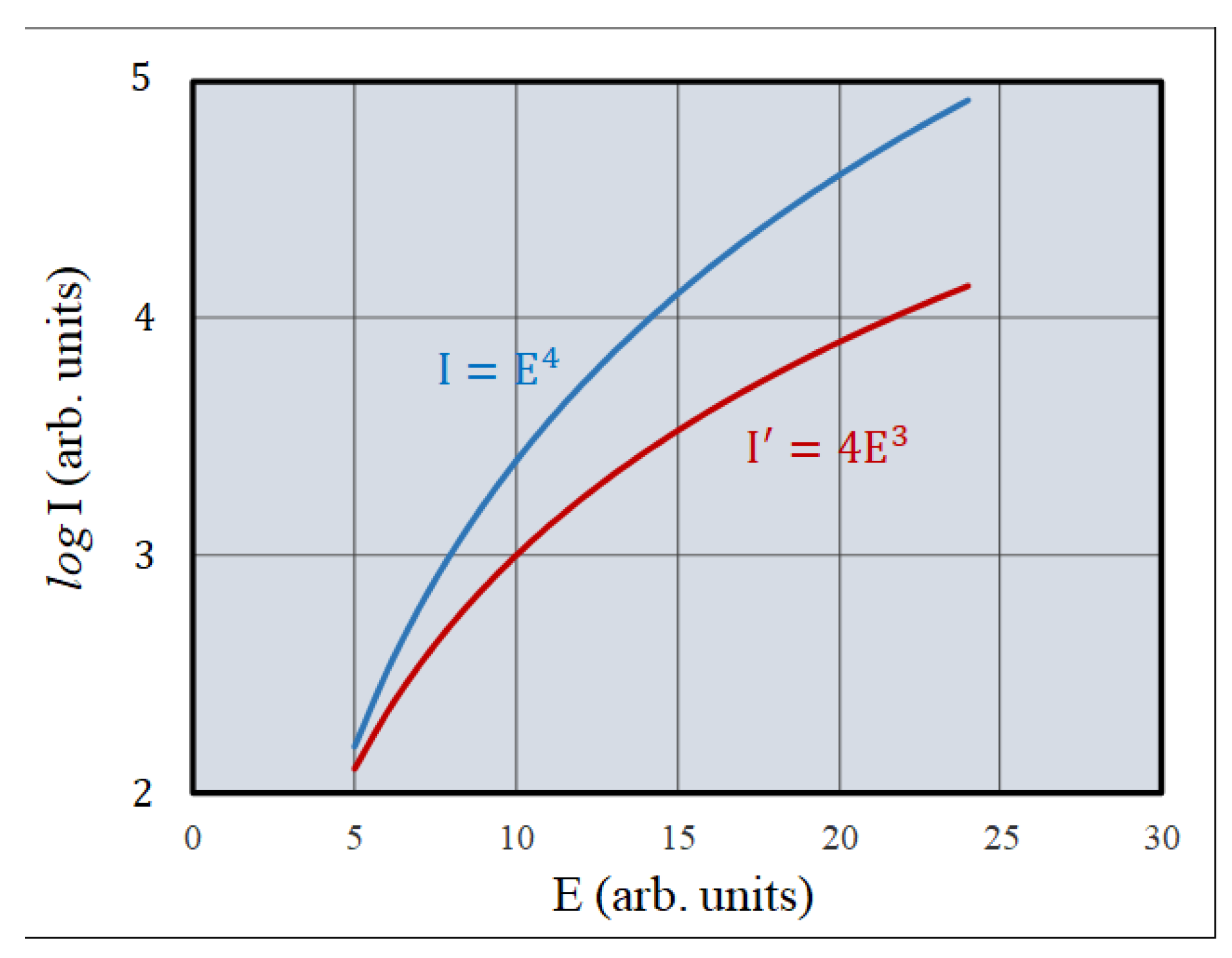
Figure 2.
Dependence of the function
Disclaimer/Publisher’s Note: The statements, opinions and data contained in all publications are solely those of the individual author(s) and contributor(s) and not of MDPI and/or the editor(s). MDPI and/or the editor(s) disclaim responsibility for any injury to people or property resulting from any ideas, methods, instructions or products referred to in the content. |
© 2025 by the authors. Licensee MDPI, Basel, Switzerland. This article is an open access article distributed under the terms and conditions of the Creative Commons Attribution (CC BY) license (http://creativecommons.org/licenses/by/4.0/).
Copyright: This open access article is published under a Creative Commons CC BY 4.0 license, which permit the free download, distribution, and reuse, provided that the author and preprint are cited in any reuse.


