
Submitted:
27 December 2025
Posted:
29 December 2025
You are already at the latest version
Abstract
In this work, hydrogenated amorphous silicon carbide (a-SiCx:H) and hydrogenated amorphous silicon oxide (a-SiOx:H) films with similar optical bandgaps (Eg), refractive indices (n), and extinction coefficients (k) were fabricated using pulse-wave modulation plasma technology by controlling the plasma turn-on and turn-off time ratio (ton/toff). These films were placed at the 1/4 position of the p/i and i/n interfaces of hydrogenated amorphous silicon (a-Si:H) p-i-n solar cells to investigate their influence on solar cell performance. Experimental results showed that when deviations in Eg, n, and k were less than 0.2%, 1.4%, and 4.1%, respectively, placing a-SiCx:H and a-SiOx:H films at the p/i and i/n interfaces increased the open-circuit voltage (Voc) and decreased the short-circuit current due to valence band (ΔEv) or conduction band (ΔEc) offsets. The reduction in cell fill factor (FF) and efficiency (η) caused by placing a-SiCx:H and a-SiOx:H films at the p/i interface was greater than that caused by placing them at the i/n interface. Placing the a-SiCx:H film at the p/i interface significantly improved the Voc. Due to the n-type doping effect of oxygen atoms, the a-SiOx:H film exhibited the lowest FF and η at the p/i interface; however, when placed at the i/n interface, it yielded FF and η values second only to the a-Si:H standard reference cell. Appropriately placing the a-SiCx:H film at the p/i interface and the slightly n-type a-SiOx:H film at the i/n interface can effectively improve the Voc, FF, and η of p-i-n solar cells.
Keywords:
a-SiCx:H
; a-SiOx:H
; p/i and i/n interfaces
; a-Si:H
; p-i-n solar cells
1. Introduction
The material properties at the p/i and i/n interfaces of hydrogenated amorphous silicon a-Si:H p-i-n solar cells influence the electric field distribution in the i-layer [1,2,3,4,5,6]. The transport of photogenerated carriers (electrons and holes) in the i-layer is primarily driven by the drift effect of the i-layer’s built-in electric field; electrons drift from the i-layer to the n-layer, while holes drift from the i-layer to the p-layer. The i-layer material properties at the p/i and i/n interfaces strongly influence the built-in electric field distribution and the collection efficiency of carriers transported to the p and n layers. Inserting high-bandgap hydrogenated amorphous silicon carbide (a-SiCx:H) or hydrogenated amorphous silicon oxide (a-SiOx:H) films at the p/i interface blocks back-diffusion of photogenerated electrons toward the p-layer via the conduction band offset (ΔEc), while the valence band offset (ΔEv) reduces the number of holes injected from the p-layer into the i-layer, which can effectively improve the open-circuit voltage (Voc) of the cell [7,8]. However, high-bandgap materials have higher defect densities, which make carriers more prone to recombination. A high ΔEv also reduces the collection efficiency of photogenerated holes crossing from the i-layer to the p-layer.
High-bandgap materials at the p/i interface can enhance the electric field intensity at the p/i interface but weaken it in the subsequent bulk region of the i-layer, making photogenerated carriers produced by short-wavelength photons at the p/i interface easier to collect. In contrast, the collection efficiency of photogenerated carriers produced by medium- and long-wavelength photons inside the i-layer decreases [1,2,3,4,5,6,9,10,11,12,13,14]. The effect of adding high-bandgap materials at the i/n interface on the built-in electric field of the i-layer is smaller than at the p/i interface. Generally, the impact on cell characteristics is lower than at the p/i interface.
Common a-SiCx:H and a-SiOx:H high-bandgap silicon-based alloy materials may exhibit different effects on the conduction and recombination of photogenerated carriers, due to distinct defect structures arising from the addition of carbon and oxygen atoms. The a-SiOx:H film exhibits n-type behavior due to micro n-type doping by oxygen atoms, meaning that in addition to the effects of band mismatch (ΔEc and ΔEv) and defect density, the a-SiOx:H film also experiences a positively charged O3+ space charge that alters the built-in electric field distribution [1,2,3,4,5,6]. Adding an a-SiOx:H high-bandgap film at the p/i interface will significantly enhance the electric field at the p/i interface due to its n-type property, while reducing the built-in electric field in the bulk region of the i-layer, causing a significant decrease in the fill factor of the cell [4,5,6,7,8,9,10,11,12,13,14]. In contrast, the a-SiCx:H film does not possess n-type properties relative to the a-SiOx:H film and does not interfere with the electric field due to the formation of space charges.
This study investigates the effects of these two materials on cell characteristics by embedding high-bandgap a-SiCx:H and a-SiOx:H films at the p/i and i/n interfaces of p-i-n solar cells. To control for variations in material characteristics, a-SiCx:H and a-SiOx:H films with similar optical bandgap (Eg), refractive index (n), and extinction coefficient (k) were selected as a baseline for comparison. We precisely controlled the optical bandgap, refractive index, and extinction coefficient (k) of these two films using pulse-wave modulation plasma technology and RF power parameters, with errors less than 4%. Under similar optical property conditions, comparing the a-SiCx:H and a-SiOx:H films placed at the p/i and i/n interfaces of a-Si:H p-i-n solar cells allows the effects of the two materials on solar cell characteristics to be distinguished. In particular, the influence of the n-type characteristics of the a-SiOx:H film on solar cell characteristics can also be distinguished.
2. Materials and Methods
Hydrogenated amorphous silicon (a-Si:H), hydrogenated amorphous silicon carbide (a-SiCx:H), and hydrogenated amorphous silicon oxide (a-SiOx:H) films, as well as p-i-n solar cells, were deposited on glass, single-crystalline silicon, and fluorine-doped tin oxide (FTO: SnO2:F) glass substrates using pulse-wave modulation plasma-enhanced chemical vapor deposition (PWM-PECVD) technology [13,14,15,16]. A 13.56 MHz radio-frequency (RF) power source controlled the on and off states of the RF power using a square-wave pulse. Plasma excitation occurred during the plasma turn-on time (ton), and plasma termination occurred during the plasma turn-off time (toff). Gases within the vacuum chamber were excited or ionized into active radicals during ton, and these active radicals were neutralized back to their original neutral gaseous state during toff. By adjusting the RF power and the ton/toff time ratio, the generation and neutralization of active radicals can be precisely regulated to control the bonding composition and the optical and electrical properties of the deposited films [13,14,15,16].
The process conditions included a fixed chamber pressure of 0.9 Torr and a substrate temperature of 210 °C. For the a-Si:H films, the SiH4/H2 flow ratio, ton/toff time, and RF power were 20/80 sccm, 20/5 ms, and 10 W, respectively. For the a-SiCx:H films, the SiH4/CH4/H2 flow rates, ton/toff time, and RF power were 20/2.5/80 sccm, 20/1 ms, and 30 W, respectively. For the a-SiOx:H films, the SiH4/CO2/H2 flow rates, ton/toff time, and RF power were 20/2.5/80 sccm, 20/5 ms, and 15 W, respectively.
Figure 1 shows schematic diagrams of the p-i-n solar cells: (a) the a-Si:H reference cell; (b) with a-SiCx:H or a-SiOx:H placed at the p/i interface; and (c) with a-SiCx:H or a-SiOx:H placed at the i/n interface. The i-layer of the a-Si:H p-i-n reference cell was a 500 nm thick a-Si:H film, serving as a baseline for comparing cell characteristics. To verify the influence of the wide-bandgap a-SiCx:H and a-SiOx:H films, the film thickness was set to 100 nm, accounting for 1/4 of the 500 nm i-layer thickness. Specifically, 1/4 of the a-Si:H film at the p/i interface (where light enters the front of the i-layer from the p-layer) and at the i/n interface (where light penetrates to the rear of the i-layer) was replaced with a-SiCx:H or a-SiOx:H films. This resulted in two types of cells with embedded buffer layers (iB): a p/iB/i/n structure of p/a-SiCx:H or a-SiOx:H (100 nm)/a-Si:H (400 nm)/n, and a p/i/iB/n structure of p/a-Si:H (400 nm)/a-SiCx:H or a-SiOx:H (100 nm)/n. The five cells were designated as follows: the reference cell (C_i a-Si:H), cells with a-SiCx:H added at the p/i interface (C_p/iB a-SiCx:H) and a-SiOx:H (C_p/iB a-SiOx:H), and cells with a-SiCx:H added at the i/n interface (C_iB/n a-SiCx:H) and a-SiOx:H (C_iB/n a-SiOx:H).
The n, k, and Eg of the a-Si:H, a-SiCx:H, and a-SiOx:H films were measured using a J. A. Woollam M2000 ellipsometer. Measurements were conducted over the wavelength range of 190–1700 nm at incident angles of 55°, 60°, 65°, and 70°. The polarization state (p- and s-planes) of light reflected from the film surface was measured to obtain amplitude and phase differences, and the thickness (d), Eg, n, and k were then simulated using the Tauc-Lorentz model [17,18]. The Si-H, Si-C, and Si-O bonding in a-SiCx:H and a-SiOx:H was measured using a Nicolet Magna 500 Fourier-transform infrared spectrometer (FTIR). The current-voltage (I-V) characteristics of the solar cells were measured using an Agilent B2912A Source Measure Unit (SMU) under AM 1.5 solar illumination provided by a SAN-EI ELECTRIC XES-40S1 solar simulator.
3. Results and Discussion
The optical and structural properties of the a-SiCx:H and a-SiOx:H films were primarily controlled by RF power and ton/toff. Figure 2 shows the Eg values of the a-SiOx:H and a-SiCx:H films. For the a-SiOx:H films, Eg gradually increased from 1.759 to 1.802 to 1.826 eV as the RF power increased from 8 to 15 to 20 W, with ton/toff = 20/5 (ms). For the a-SiCx:H films, due to the lower dissociation efficiency of CH4, Eg increased only from 1.777 to 1.794 eV when the RF power was raised from 25 to 30 W under the condition of ton/toff = 20/5 (ms). To increase Eg, the ton/toff ratio was increased to 20/1 (ms), yielding an Eg of 1.806 eV. The difference in bandgap (Eg) between the 1.802 eV a-SiOx:H film and the 1.806 eV a-SiCx:H film was less than 0.2%; thus, a-SiOx:H and a-SiCx:H films under these conditions were used as buffer layer materials.
To ensure the relative relationship between the refractive index (n) and extinction coefficient (k) of the a-SiOx:H and a-SiCx:H films, the Tauc–Lorentz model [17,18] was used for analysis. Figure 3 presents (a) the full spectrum of n and (b) k for a-Si:H, a-SiCx:H, and a-SiOx:H films from 190 to 1680 nm, along with (c) the difference in n between a-SiCx:H and a-SiOx:H films (Δn) divided by the n value of the reference a-Si:H film (na-Si:H), i.e., Δn/na-Si:H, and (d) the difference in k (Δk) divided by the k value of the reference a-Si:H film (ka-Si:H), i.e., Δk/ka-Si:H. These variations are defined as follows: equations (1) and (2):
Figure 3a and Figure 3b show that the n and k values of the wide-bandgap a-SiCx:H and a-SiOx:H films were close to each other but lower than those of the a-Si:H film used in the reference cell. Figure 3c presents the Δn/na-Si:H of the a-SiCx:H and a-SiOx:H films, with a very small variation error ranging from +1.4% to -0.98%. The refractive index (n) values of the a-SiCx:H and a-SiOx:H films were nearly identical. Figure 3d shows the Δk/ka-Si:H of the a-SiCx:H and a-SiOx:H films, with a variation error ranging from +1.2% to -4.1%. Although slightly larger than Δn/na-Si:H, the values remained very small, indicating that the k values of the a-SiCx:H and a-SiOx:H films were also close to each other. The selected a-SiCx:H and a-SiOx:H films possessed similar properties in terms of Eg, n, and k. Under these conditions, the effects on the p/i and i/n interfaces could be comparatively analyzed; in particular, the n-type doping effect of the a-SiOx:H film compared to the a-SiCx:H film could be examined under conditions of similar optical characteristics.
To confirm the differences in Si-H, Si-C, and Si-O bonding between the a-SiCx:H and a-SiOx:H films, Figure 4 shows the FTIR spectra of 200 nm thick a-SiCx:H and a-SiOx:H films for (a) the wagging and bending bands and (b) the stretching band. Figure 4a shows that the a-SiCx:H film had a larger absorbance amplitude in the wagging mode (540 to 750 nm) (integrated area Ia-SiCx:H of 9.221). The difference dABS = Ia-SiCx:H - Ia-SiOx:H in integrated area between the a-SiCx:H and a-SiOx:H films (Ia-SiOx:H = 8.472) was 0.7490, which is approximately 8.1% of the a-SiCx:H film area (0.7490/9.221 = 8.1%). The difference between the two films in the main Si-H bond intensity was not significant. The stretching mode of the Si-C bond was primarily located at the peak position of 774 cm−1. In the 930 to 1130 cm−1 range, weak Si-O-Si bonding at 960 cm−1, Si(Si2-O2) at 1012 cm−1, and Si-O-Si bonding at 1100 cm−1 [19,20,21,22,23] were observed, with an integrated peak intensity of approximately Ia-SiCx:H = 1.080 in the 750 to 1130 cm−1 range. The a-SiOx:H film exhibited significantly stronger Si-O-Si bonding at 785, 818, 960, 1005, and 1090 cm−1, with an integrated peak intensity Ia-SiOx:H of approximately 5.352 in the 750 to 1130 cm−1 range. The difference dABS = Ia-SiOx:H - Ia-SiCx:H in the integrated area of oxygen content intensity for the a-SiOx:H film compared to the a-SiCx:H film (Ia-SiCx:H = 1.080) was 4.272, which is approximately 80% higher relative to the a-SiOx:H film area (4.272/5.352 = 80%). This result indicates that the primary difference between the two films stems from the distinction in oxygen content.
Figure 4b shows the absorbance intensity of the stretching mode and the difference between the a-SiCx:H and a-SiOx:H films. The a-SiCx:H film had a larger amplitude in the stretching mode (1920 to 2150 nm) (integrated area Ia-SiCx:H of 3.418). The difference between the integrated areas of the a-SiCx:H and a-SiOx:H films was 0.4850, which is approximately 14% of the a-SiCx:H film area (0.4850/3.418 = 14%). The FWHM of the a-SiCx:H film in this 14% range was approximately between 1961 and 2078 cm−1, indicating more mono-hydride (SiH) bonds and a small amount of di-hydride (SiH2) bonds. Although the optical properties of the a-SiCx:H and a-SiOx:H films were similar, the bonding structure differed. The a-SiCx:H film showed an 8% increase in hydrogen content and a 14% increase in mono-SiH bonding compared to the a-SiOx:H film. Conversely, the a-SiOx:H film showed an 80% increase in oxygen content compared to the a-SiCx:H film.
Figure 5 presents the I-V characteristic curves for the reference cell and the four test cells containing a-SiCx:H and a-SiOx:H buffer layers in the 1/4 region of the p/i and i/n interfaces. The curves cover (a) 0 to open-circuit voltage (Voc), (b) -0.5 to 0 V reverse bias, and (c) Voc to 1.0 V forward bias ranges. The data for short-circuit current density (Jsc), Voc, maximum output current density (Jm), maximum output voltage (Vm), maximum output power (Pmax), fill factor (FF), and efficiency (η) of the five cells are listed in Table 1.
Figure 5a shows that the reference cell C_i a-Si:H had the maximum Jsc of 13.38 mA/cm2, the minimum Voc of 0.8369 V, the maximum Jm, Vm, and FF of 11.31 mA/cm2, 0.6800 V, and 68.69%, respectively, and the maximum efficiency η of 7.692%. In the four test cells, Jsc was consistently lower than that of the reference cell C_i a-Si:H, and Voc was consistently higher. The FF values for cells with buffer layers at the p/i interface (57.82% and 43.99%) were significantly lower than those for cells with buffer layers at the i/n interface (64.84% and 67.38%, respectively). Figure 5b shows the variation in current density (J) from -0.5 to 0 V. In this range, the J of the four test cells remained lower than that of the reference cell. Notably, the C_p/iB a-SiOx:H sample with a-SiOx:H at the p/i interface showed a current that gradually increased from the second lowest -13.00 mA/cm2 to the second highest -13.56 mA/cm2 as the voltage went from 0 to -0.5 V. At the same time, the magnitude relationship of the J values for the other three cells remained basically unchanged. This result indicates that when a-SiOx:H is placed at the p/i interface, J increases rapidly with increasing reverse bias; that is, photogenerated carriers in the i-layer can continuously increase the current because the reverse bias enhances the electric field intensity in the i-layer. Figure 5c shows the variation in J from Voc to 1.0 V forward bias. Within this range, the increase in the four test cells was smaller than that in the reference cell. For example, at 0.915 V, the current density increased sequentially from the minimum of 1.988 mA/cm2 for C_p/iB a-SiCx:H, to 8.998 mA/cm2 for C_p/iB a-SiOx:H, 9.995 mA/cm2 for C_iB/n a-SiCx:H, and 11.21 mA/cm2 for C_iB/n a-SiOx:H. This indicates that the effect of a-SiCx:H and a-SiOx:H films was greater at the p/i interface than at the i/n interface, with a-SiCx:H showing a greater effect than a-SiOx:H. This demonstrates that the impact of a-SiCx:H and a-SiOx:H films at the p/i interface on blocking hole injection from the p-layer into the i-layer was higher than their impact on blocking electron injection from the n-layer into the i-layer. The minimum current of 1.988 mA/cm2 for C_p/iB a-SiCx:H corresponded to its maximum Voc value of 0.8998 V, demonstrating its effectiveness in improving Voc. The similar effects observed for C_p/iB a-SiOx:H (8.998 mA/cm2), C_iB/n a-SiCx:H (9.995 mA/cm2), and C_iB/n a-SiOx:H (11.21 mA/cm2) indicate that the influence of a-SiOx:H at the p/i and i/n interfaces and a-SiCx:H at the i/n interface was comparable.
The cell with the a-SiOx:H p/i buffer layer had the lowest FF of 43.99%, while the cell with the i/n buffer layer had the second-highest FF (67.38%). This is distinct from the cell with the a-SiCx:H p/i buffer layer, which had a slightly higher FF (57.82%), while the cell with the i/n buffer layer had a lower FF (64.84%). Placing a-SiCx:H and a-SiOx:H buffer layers at the p/i interface improved the open-circuit voltage; the a-SiCx:H film increased it to 0.8998 V, higher than the 0.8482 V of the a-SiOx:H film. This implies that the valence band offset (ΔEv) in the a-SiCx:H film was higher than that in the a-SiOx:H film. Because this energy barrier is more difficult to cross, there was greater blocking of holes injected from the p-layer into the i-layer or of photogenerated holes flowing from the i-layer to the p-layer, resulting in a larger Voc with the addition of the a-SiCx:H film. The significant decrease in FF (43.99%) caused by the a-SiOx:H film had a low correlation with the valence band offset (ΔEv). Instead, it was due to the micro n-type doping of oxygen atoms in the a-SiOx:H film, which caused misalignment and a reduction of the built-in electric field in the subsequent i-layer, leading to a significant reduction in overall efficiency when the a-SiOx:H film was added to the p/i buffer layer. This is also reflected in the fact that when the a-SiOx:H film was moved to the i/n interface, the n-type doping enhanced the built-in electric field of the entire i-layer, resulting in the a-SiOx:H film at the i/n interface achieving the second-highest fill factor (67.38%), only slightly lower than that of the a-Si:H reference cell [13,14].
The overall performance of cells with a-SiCx:H and a-SiOx:H films at the i/n interface was significantly lower than that of cells with these films at the p/i interface. This indicates that the conduction band offset (ΔEc) at the i/n interface had a minor impact on cell transport. Since the open-circuit voltages were higher than that of the reference cell (0.8486 and 0.8487 V), ΔEc still had a particular influence on electron output or input. However, the fill factor was significantly improved, indicating that placement at the i/n interface had a minor impact on the built-in electric field intensity in the i-layer. The a-SiOx:H film had the lowest fill factor of 43.99% when placed at the p/i interface, but achieved the second-highest of 67.38% when placed at the i/n interface; this can be attributed to the weakening of the i-layer built-in electric field at the p/i interface and the strengthening effect at the i/n interface caused by the n-type doping effect of the a-SiOx:H film. Regarding short-circuit current density, the a-SiCx:H film placed at the i/n interface had the second-highest value of 13.21 mA/cm2, indicating a minor impact on photogenerated electron tunneling, whereas the a-SiOx:H film had the lowest value of 12.99 mA/cm2, indicating a slightly larger impact on photogenerated electron tunneling, causing a decrease in current value.
The experimental results above indicate that a-SiCx:H and a-SiOx:H films at the p/i interface have a greater attenuation effect on the fill factor. The electric field is too concentrated between the p-layer and these two buffer layers, weakening it in the subsequent i-layer and causing a significant drop in FF; this effect is more pronounced for the a-SiOx:H film due to its slight n-type doping. Conversely, a-SiCx:H at the p/i interface significantly increases the Voc value due to a higher ΔEv effect. The degradation of the fill factor by a-SiCx:H and a-SiOx:H films at the i/n interface is less pronounced than at the p/i interface. This suggests that the built-in electric field of the i-layer extends effectively throughout the entire i-region, and the n-type doping effect of a-SiOx:H further enhances the electric field intensity throughout the i-layer, resulting in the second-highest fill factor. This is a significant distinction in the application of a-SiOx:H and a-SiCx:H films. Regardless of placement at the p/i or i/n interface, the open-circuit voltage is higher, and the short-circuit current is lower than those of the reference cell, with band mismatches ΔEv and ΔEc contributing. Part of the Jsc decrease at the i/n interface is also due to reduced generation of photogenerated carriers from medium- or long-wavelength photons.
4. Conclusions
In this study, a-SiCx:H and a-SiOx:H films with approximately identical optical bandgaps (Eg) were fabricated using pulse-wave modulation plasma and placed at the p/i and i/n interfaces. Because the optical bandgaps were similar, the influence of n-type doping in the a-SiOx:H film could be inferred. Experimental results showed that n-type doping in the a-SiOx:H film significantly reduced the electric field intensity in the i-layer at the p/i interface while increasing it at the i/n interface. This was reflected in a significant reduction in FF at the p/i interface and a substantial increase in FF at the i/n interface. Both ΔEc and ΔEv of the two films contributed to the increase in the open-circuit voltage (Voc) of the cells. Appropriately placing the a-SiCx:H film at the p/i interface and the a-SiOx:H film at the i/n interface can improve the open-circuit voltage, fill factor, and efficiency of p-i-n solar cells.
Acknowledgments
The authors thank Kun-Hsien Wu, Yi-Zhen Hong, Chun-Jan Nien, and Ting-Yu Hu for assisting with the figures. This work was supported by the Ministry of Science and Technology, R.O.C. (grant number 111-2221-E-005-028-).
References
- Shimizu, T.; Kidoh, H.; Morimoto, A.; Kumeda, M. Nature of localized states in hydrogenated Si–based amorphous semiconductor films elucidated from LESR and CPM. Jpn. J. Appl. Phys. 1989, 28, 586–592. [Google Scholar] [CrossRef]
- Shimizu, T.; Matsumoto, M.; Yoshita, M.; Iwami, M.; Morimoto, A.; Kumeda, M. Influence of N, O and C impurities in a-Si:H. J. Non Cryst. Solids 1991, 137-138, 391–394. [Google Scholar] [CrossRef]
- Morimoto, A.; Matsumoto, M.; Yoshita, M.; Kumeda, M.; Shimizu, T. Doping effect of oxygen or nitrogen impurity in hydrogenated amorphous silicon films. Appl. Phys. Lett. 1991, 59, 2130–2132. [Google Scholar] [CrossRef]
- Hishikawa, Y.; Isomura, M.; Okamoto, S.; Hashimoto, H.; Tsuda, S. Effects of the i- layer properties and impurity on the performance of a-Si solar cell. Sol. Energy Mater. Sol. Cells 1994, 34, 303–312. [Google Scholar] [CrossRef]
- Isomura, M.; Kinoshita, T.; Hishikawa, Y.; Tsuda, S. Influence of oxygen impurity in the intrinsic layer of amorphous silicon solar cells. Appl. Phys. Lett. 1994, 65, 2329–2331. [Google Scholar] [CrossRef]
- Kinoshita, T.; Isomura, M.; Hishikawa, Y.; Tsuda, S. Influence of oxygen and nitrogen in the intrinsic layer of a-Si:h solar cells. Jpn. J. Appl. Phys. 1996, 35, 3819–3824. [Google Scholar] [CrossRef]
- Vet, B.; Zeman, M. Relation between the open-circuit voltage and the band gap of absorber and buffer layers in a-Si:H solar cells. Thin Solid Films 2008, 516, 6873–6876. [Google Scholar] [CrossRef]
- Yue, G.; Yan, B.; Teplin, C.; Yang, J.; Guha, S. Optimization and characterization of i/p buffer layer in hydrogenated nanocrystalline silicon solar cells. J. Non Cryst. Solids 2008, 354, 2440–2444. [Google Scholar] [CrossRef]
- Woerdenweber, J.; Merdzhanova, T.; Schmitz, R.; Mück, A.; Zastrow, U.; Niessen, L.; Gordijn, A.; Carius, R.; Beyer, W.; Stiebig, H.; Rau, U. Influence of base pressure and atmospheric contaminants on a-Si:h solar cell properties. J. Appl. Phys. 2008, 104, 094507. [Google Scholar] [CrossRef]
- Woerdenweber, J.; Merdzhanova, T.; Stiebig, H.; Beyer, W.; Gordijn, A. Critical oxygen concentration in hydrogenated amorphous silicon solar cells dependent on the contamination source. Appl. Phys. Lett. 2010, 96, 103505. [Google Scholar] [CrossRef]
- Woerdenweber, J.; Merdzhanova, T.; Gordijn, A.; Stiebig, H.; Beyer, W. Incorporation and critical concentration of oxygen in a-Si:H solar cells. Sol. Energy Mater. Sol. Cells 2011, 95, 2811–2815. [Google Scholar] [CrossRef]
- Merdzhanova, T.; Woerdenweber, J.; Beyer, W.; Kilper, T.; Zastrow, U.; Meier, M.; Stiebig, H.; Gordijn, A. Impurities in thin-film silicon: influence on material properties and solar cell performance. J. Non Cryst. Solids 2012, 358, 2171–2178. [Google Scholar] [CrossRef]
- Kuo, T.C.; Jiang, Y.L. Residual impurities in a process chamber on the characteristics of a-Si:H solar cells. Sol. Energy Mater. Sol. Cells 2013, 117, 617–623. [Google Scholar] [CrossRef]
- Jiang, Yeu-Long; Hong, Cheng-Wei. Pulsed-plasma spatial modulation of i-layer structures and oxygen impurity profiles of hydrogenated amorphous silicon solar cells. J. Non Cryst. Solids 2022, 591, 121737. [Google Scholar] [CrossRef]
- Jiang, Y.L.; Shih, P.T.; Kuo, T.C. Hydrogenated amorphous silicon a-Si:Hx /a-Si:Hy compositional superlattices: profiling the lattice-constant-scale spatial change of the designed Si–H bonding configurations. Appl. Phys. Lett. 2008, 92, 101915. [Google Scholar] [CrossRef]
- Ahnood, A.; Suzuki, Y.; Madan, A.; Nathan, A. Pulsed-radio frequency plasma enhanced chemical vapour deposition of low temperature silicon nitride for thin film transistors. Thin Solid Films 2012, 520, 4831–4834. [Google Scholar] [CrossRef]
- Fujiwara, H.; Collins, R.W., Spectroscopic Ellipsometry for Photovoltaics, Volume 1: Fundamental Principles and Solar Cell Characterization, Springer, Cham, Switzerland, 2018; pp. 141–143.
- Patel, D.I.; Shah, D.; Hilfiker, J.N.; Linford, M.R. A tutorial on spectroscopic ellipsometry (SE), 5. using the tauc-lorentz and cody-lorentz models to describe the absorption features of amorphous silicon (a-Si). Vac. Technol. Coat. 2019, 34–37. [Google Scholar]
- Das, Debajyoti; Samanta, Subhashis. Reverse Meyer-Neldel rule prevailing in the hole transport of B-doped nc-SiOx:H thin films sustaining degeneracy and performing as suitable window of nc-Si solar cells. Physica E: Low-dimensional Systems and Nanostructures 2021, 128, 114615. [Google Scholar] [CrossRef]
- Samanta, Arup; Das, Debajyoti. Studies on the structural properties of SiO:H films prepared from (SiH4+CO2+He) plasma in RF-PECVD. Solar Energy Materials & Solar Cells 2009, 93, 588–596. [Google Scholar]
- Das, Debajyoti; Samanta, Subhashis. Advanced nanocrystallinity with widened optical gap realized via microstructural control in P-doped silicon oxide thin films used as window layer in nc-Si solar cells. Materials Chemistry and Physics 2020, 243, 122628. [Google Scholar] [CrossRef]
- Ahmad, Gufran; Mandal, Sourav; Barua, Asok Kumar; Bhattacharya, Tarun K.; Roy, Jatindra Nath. Band offset reduction at defect-rich p/i interface through a wide bandgap a-SiO:H buffer layer. IEEE Journal of Photovoltaics 2017, 7(2), 414–420. [Google Scholar] [CrossRef]
- Kanekoa, Tsutomu; Nemotoa, Dai; Horiguchia, Atsushi; Miyakawa, Nobuaki. FTIR analysis of a-SiC:H films grown by plasma enhanced CVD. Journal of Crystal Growth 2005, 275, 1097–1101. [Google Scholar] [CrossRef]
Figure 1.
Schematic diagram of the p-i-n solar cells: (a) the a-Si:H reference cell; (b) with a-SiCx:H or a-SiOx:H placed at the p/i interface; and (c) with a-SiCx:H or a-SiOx:H placed at the i/n interface.
Figure 1.
Schematic diagram of the p-i-n solar cells: (a) the a-Si:H reference cell; (b) with a-SiCx:H or a-SiOx:H placed at the p/i interface; and (c) with a-SiCx:H or a-SiOx:H placed at the i/n interface.
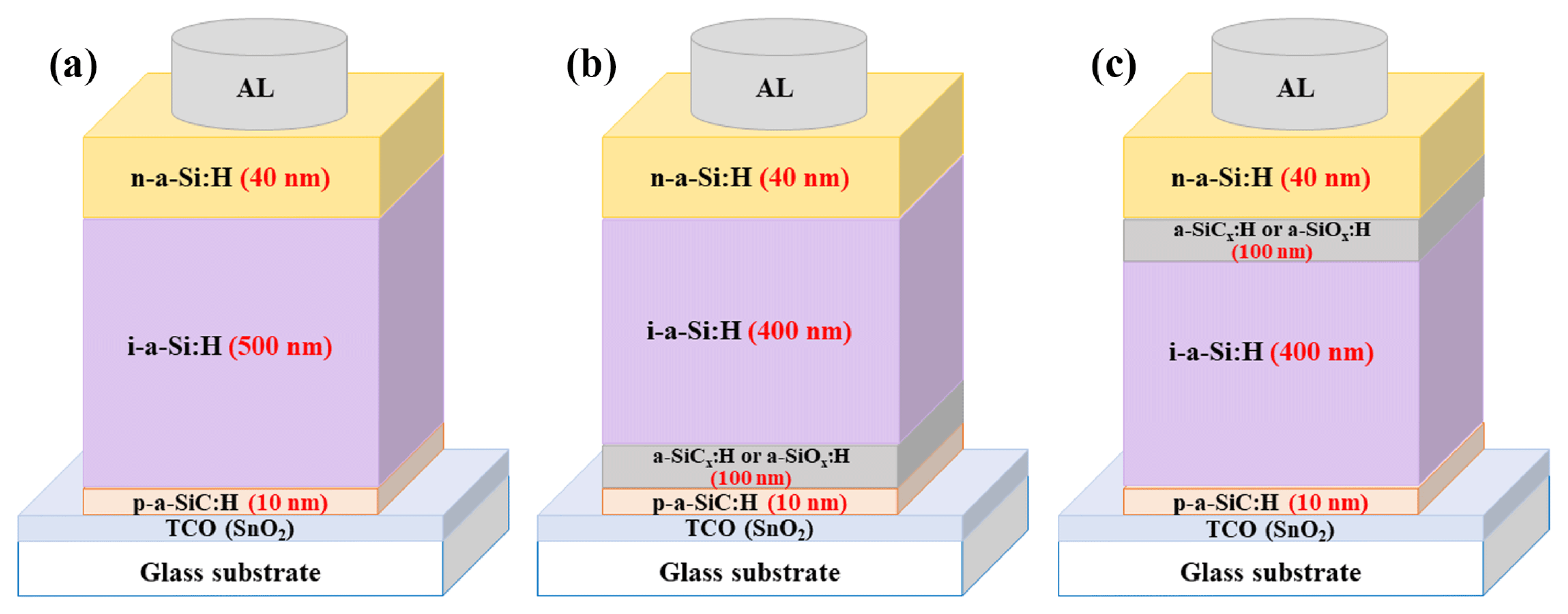
Figure 2.
Optical bandgap Eg values of a-SiOx:H and a-SiCx:H films fabricated using RF power and ton/toff ratios.
Figure 2.
Optical bandgap Eg values of a-SiOx:H and a-SiCx:H films fabricated using RF power and ton/toff ratios.
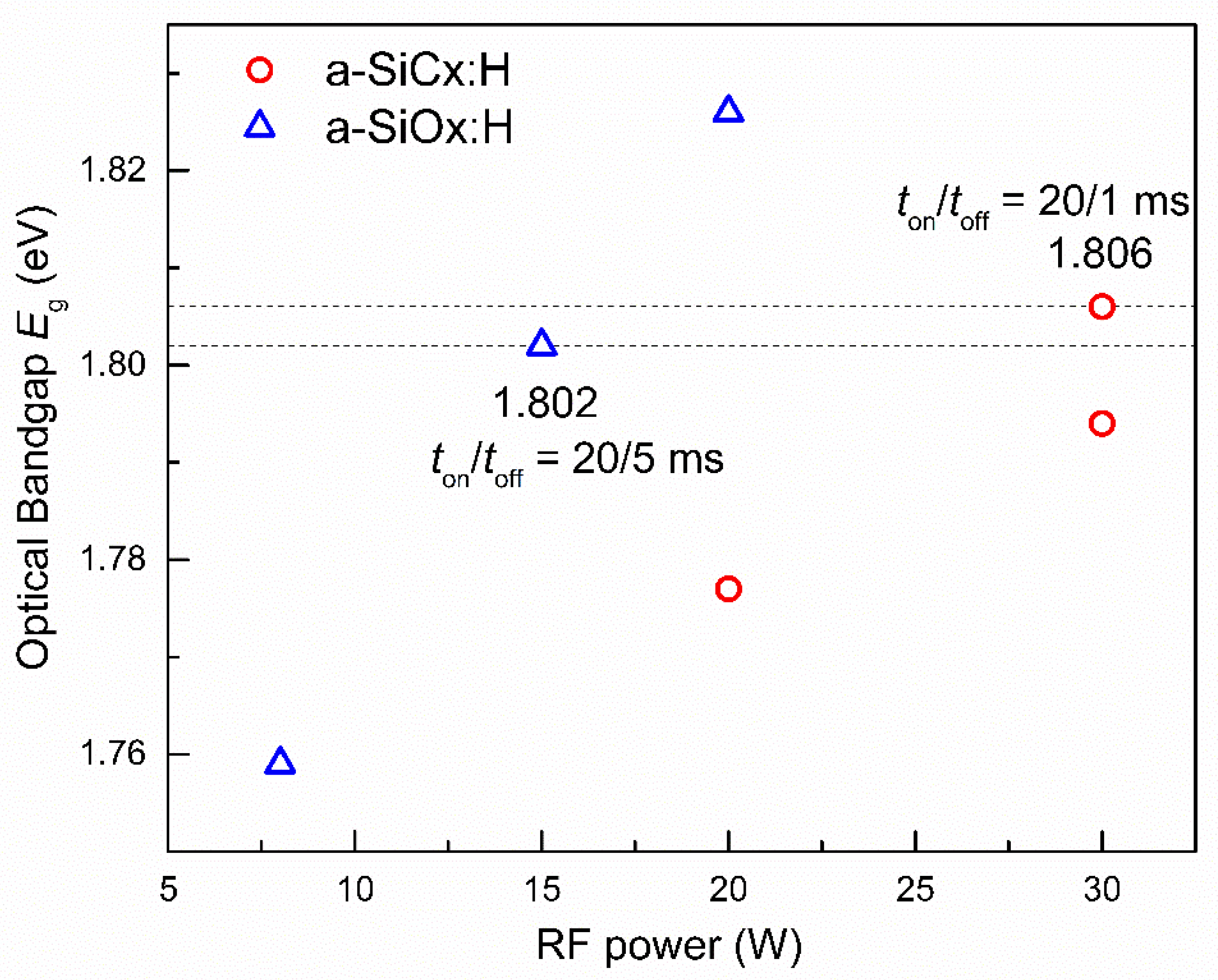
Figure 3.
(a) Refractive index (n) and (b) extinction coefficient (k) of a-Si:H, a-SiCx:H, and a-SiOx:H films; (c) Δn/na-Si:H and (d)Δk/ka-Si:H of a-SiCx:H and a-SiOx:H films.
Figure 3.
(a) Refractive index (n) and (b) extinction coefficient (k) of a-Si:H, a-SiCx:H, and a-SiOx:H films; (c) Δn/na-Si:H and (d)Δk/ka-Si:H of a-SiCx:H and a-SiOx:H films.
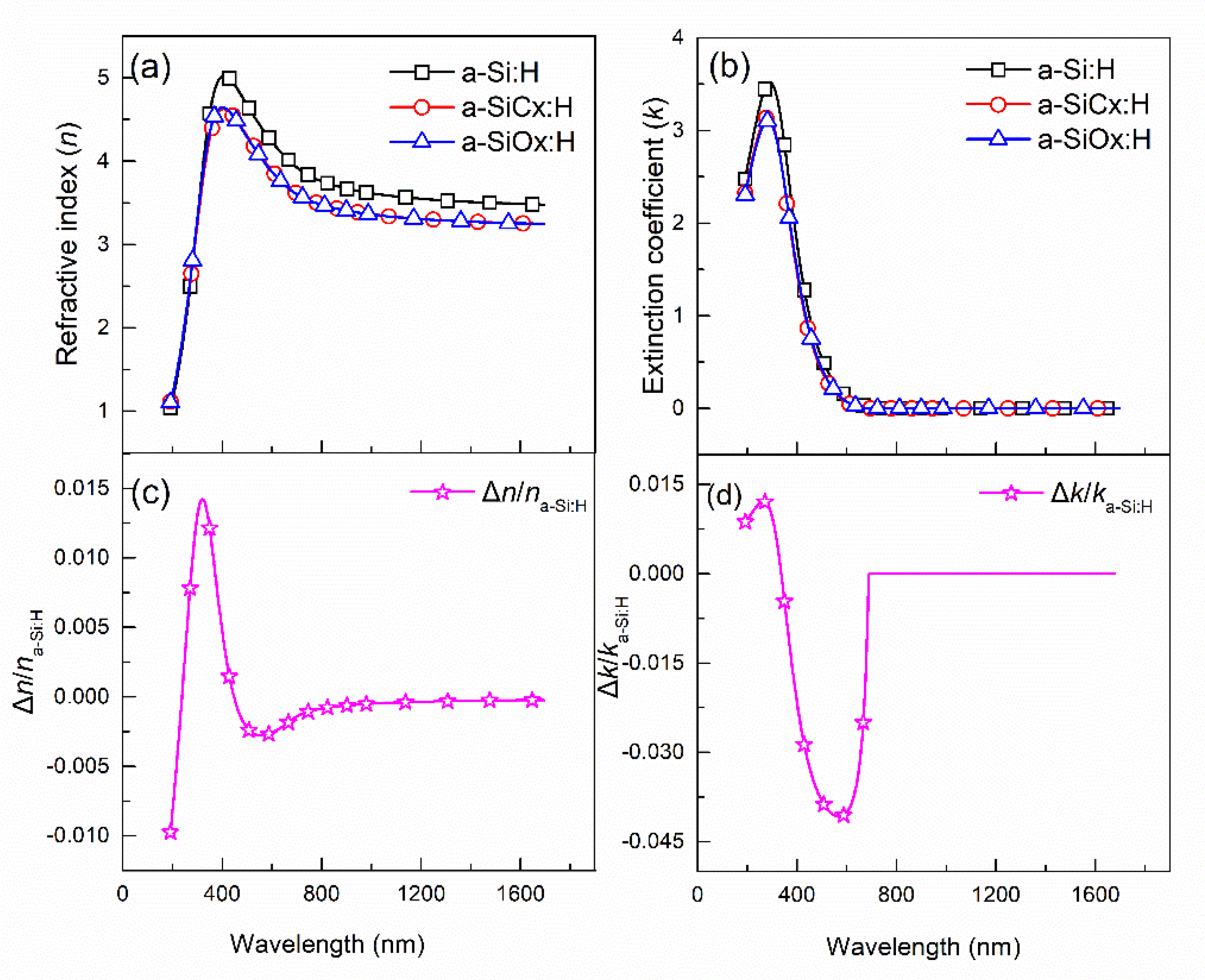
Figure 4.
FTIR spectra of a-SiCx:H and a-SiOx:H films with a thickness of 200 nm: (a) wagging and bending modes; and (b) stretching modes.
Figure 4.
FTIR spectra of a-SiCx:H and a-SiOx:H films with a thickness of 200 nm: (a) wagging and bending modes; and (b) stretching modes.
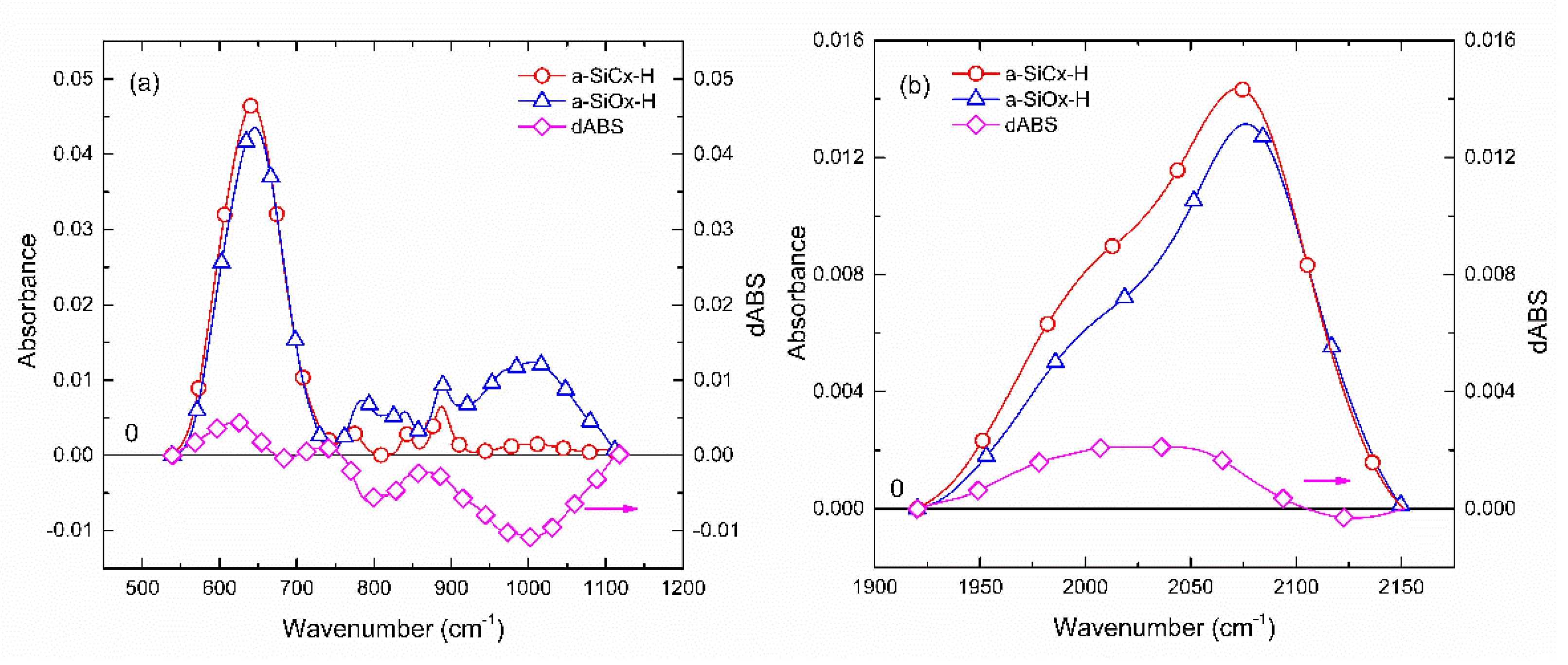
Figure 5.
Current–voltage (I−V) characteristics of the five cells, including the reference cell and cells with a-SiCx:H and a-SiOx:H buffer layers at the 1/4 position of the p/i and i/n interfaces: (a) range from 0 to Voc; (b) reverse bias range from -0.5 to 0 V; and (c) forward bias range from Voc to 1.0 V.
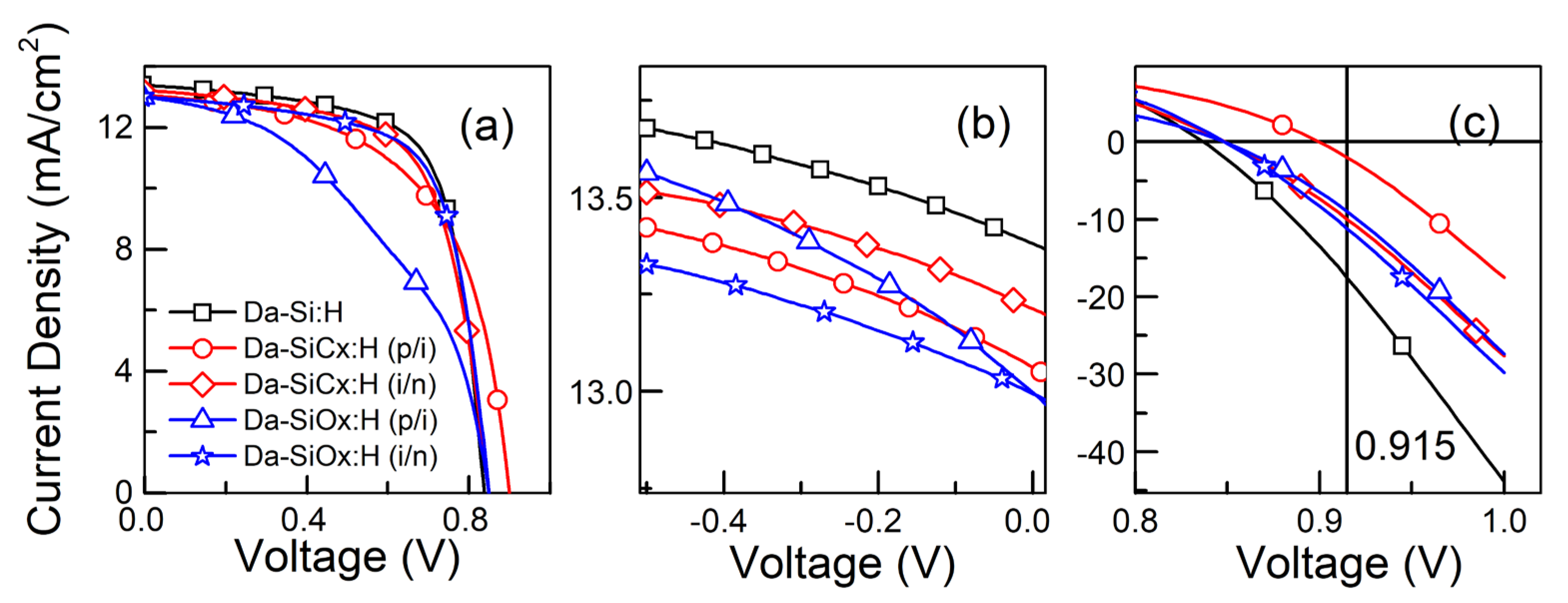

Table 1.
The short-circuit current density (Jsc), Voc, maximum output current density (Jm), maximum output voltage (Vm), maximum output power (Pmax), and efficiency (η) of the five cells.
Table 1.
The short-circuit current density (Jsc), Voc, maximum output current density (Jm), maximum output voltage (Vm), maximum output power (Pmax), and efficiency (η) of the five cells.
|
Jsc (mA/cm2) |
Voc (V) |
Jm (mA/cm2) |
Vm (V) |
FF (%) |
Pmax (mW) |
η (%) |
|
| C_a-i:H | 13.38 | 0.8369 | 11.31 | 0.6800 | 68.69 | 0.5437 | 7.692 |
| C_ p/iB a-SiCx:H |
13.06 | 0.8998 | 9.994 | 0.6800 | 57.82 | 0.4804 | 6.796 |
| C_ p/iB a-SiOx:H |
13.00 | 0.8482 | 8.738 | 0.5550 | 43.99 | 0.3428 | 4.850 |
| C_iB/n a-SiCx:H |
13.21 | 0.8486 | 11.02 | 0.6600 | 64.84 | 0.5139 | 7.270 |
| C_iB/n a-SiOx:H |
12.99 | 0.8487 | 10.93 | 0.6800 | 67.38 | 0.5252 | 7.430 |
Disclaimer/Publisher’s Note: The statements, opinions and data contained in all publications are solely those of the individual author(s) and contributor(s) and not of MDPI and/or the editor(s). MDPI and/or the editor(s) disclaim responsibility for any injury to people or property resulting from any ideas, methods, instructions or products referred to in the content. |
© 2025 by the authors. Licensee MDPI, Basel, Switzerland. This article is an open access article distributed under the terms and conditions of the Creative Commons Attribution (CC BY) license (http://creativecommons.org/licenses/by/4.0/).
Copyright: This open access article is published under a Creative Commons CC BY 4.0 license, which permit the free download, distribution, and reuse, provided that the author and preprint are cited in any reuse.


