Submitted:
23 December 2025
Posted:
24 December 2025
You are already at the latest version
Abstract
The 2-D Ti3C2 (MXene) materials have found applications in various fields, partic-ularly as a candidate for field emission electron source when mixed with carbon nano-tubes (CNTs) as the electron source material. In this study, a novel multilayer film structure utilizing Ti₃C₂ (MXene) / CNTs and fabricate a unique field emitter device using these 2-D Ti3C2 (MXene) / CNT materials have been presented. The material ex-hibits a tensile stress of 950 MPa and a low elongation at break of 8%. Specifically, uti-lizing the sharp edges of this material for emission, the field emission characteristics of Ti3C2 (MXene) and Ti3C2 (MXene) / CNT have been compared. The field emission char-acteristics of Ti3C2 (MXene) and Ti3C2 (MXene) / CNT have been compared. Measuring the current density is up to 3.49 A∙cm-2 at an electric field of 2.91 V∙µm−1, It has low turn-on field (Eon) 1.6 V∙ m-1, and low threshold electric field (Eth) 0.22 μA.cm-2. The field enhancement factor β of Ti3C2 (MXene) / CNT is about 4.5 times more than pristine Ti3C2 (MXene). Utilizing curved tip of Ti3C2 (MXene) / CNT emission, the field emission current device slightly increases surround the vacuum degree from 1.010-3 Pa to 4.710-5, and the current can be emitted steadily for a duration of 1 hour under the voltage of 723 V and vacuum level of 1.010-3 Pa. Those results provide that this kind of multilayer film Ti₃C₂ (MXene) / CNT exhibits exceptional mechanical properties and can be easily shaped, particularly suit to fabricate vacuum electronic devices and other uses.
Keywords:
field emission
; Ti3C2 (MXene )
; CNT
1. Introduction
2-D Ti3C2 (MXene) materials have found applications in various fields [1,2], including energy storage, supercapacitors and batteries [3], biomedicine [4], catalysis [5], environmental detection and so on. However, the two-dimensional MXene material exhibits relatively low mechanical properties, including tensile strength and elongation, and is very vulnerable to moisture due to its hydrophilicity. In oder to enhance its elasticity, researchers have successfully fabricated composited devices by combining MXene with other materials, such as carbon fiber, expanded graphite, graphene, and even CNT, all of which possess exceptional electrical conductivity and flexibility [6]. Such as Rajasmita Malik and his team used MXene composite polymer (EMA) s with a concentration of 10% to make an elastic electron storage device [7]. And mix graphene oxide or carbon nanotubes can be increase its strength and reduce infrared absorption [8,9]. Mengyao Xu and his team adopted the autocatalytic growth of CNTs on Ti3C2Tx nanosheets at low temperature and combined with the thermal annealing technology in nitrogen atmosphere to prepare a mixture of Ti3C2TX-cnts [10]. As electromagnetic interference (EMI) shielding materials [11,12], Hao Wu's team used a natural rubber NR and combined it into a "sandwich" structure of a composite membrane of NR / MXene / CNTs to enhance its durability and thermoelectric conversion, as well as hydrophobic. Its mechanical strength of multilayer NR / MXene / CNTs-50 has a tensile stress of 20.7 MPa and elongation at break of 123.2% [13].
The materials can also be used in microwave absorption (MA) materials [14,15]. but the electric field emission properties of their structures in lower vacuum are rarely studied. Here, we utilized the vacuum-assisted filtration system and employed to fabricate a multilayer film of Ti₃C₂ (MXene) / CNT. The measurement techniques have been employed to analyze the properties of MXene materials, such as SEM, x-ray diffraction (XRD) [16], field emission scanning electron microscopy (FESEM).
The characteristics of electric field emission are affected by the surrounding atmosphere. By utilizing vacuum assistance, the device’s emitter can be measured in a vacuum environment, which can reduce the work function of materials [17]. MXene exhibits high electrical conductivity values, such as metal-like electrical conductivity reaching ≈20000 S∙cm−1, while nanotubes show semiconducting or metallic electronic properties. However, these materials are susceptible to sputter erosion and chemical contamination, which negatively impact their field emission behavior and result in degradation. Therefore, high vacuum conditions are necessary for operation [18].
Since 2020, Yan et al reported the utilization of 2D Ti3C2 (MXene) as a cold field emission cathode material under the vacuum pressure of 10-6 Pa. They achieved a measured current density of 59 mA∙ cm−2 at an electric field strength of 7.5 V∙µm−1. They further investigated the MXene–TiO2 composite and measured an enhanced emission current density reaching up to 289 mA∙cm−2 from the cross-section of the composite film at a pressure of 1.0 × 10⁻⁵ Pa [19,20].
Based on previous study, Utilizing the sharp edge of this material for emission, a field emitter device using 2-D Ti3C2 (MXene) material and Ti3C2 (MXene) Mixing CNT have been fabricated respectively.
2. Experimental Section
2.1. Materials
The production of few-layer Ti3C2 (MXene) can be achieved by utilizing various etchants and delamination techniques [21]. The wet-chemical etching methods commonly employed at the earliest stage involve the utilization of hydrofluoric acid (HF) or HF-containing solutions.the process can be represented by following equation: [22,23]. Obviously , HF has more hazardous, In the current year, Ti3AlC2 Mixture lithium fluoride (LiF) and concentrated hydrochloric acid (HCl) produced in situ HF to obtained Ti3C2. The delaminated solution of few-layer Ti3C2 (MXene) was obtained using this method and purchased from Jilin 11 Technology Co., Ltd
The cross-stacked CNT films were fabricated using super-aligned carbon nanotubes. First, individual CNTs are extracted using tweezers. These individual tubes are then assembled into an initial ribbon without any interruptions. This initial thin ribbon is further extended to form a CNT film of the same width as the substrate. Finally, by stacking multiple layers of superaligned CNT films in a crosswise manner, a "cross-stack film" could be produced [24,25].
2.2. Preparation of Ti3C2 (MXene)/CNTs Films
A schematic illustration of the preparation process for the Ti3C2 (MXene) / CNT film ( Figure 1), shows that the fabrication of Ti3C2 (MXene) / CNT hybrid films involved a mixing filtration technique. Firstly, about 5 mg / ml aqoeous solution Ti3C2 (MXene) suspension was initially subjected to a 30-minute ultrasonic treatment as an initial step. The solutions should be subjected to vacuum filtration, with a volume of approximately 0.2ml each., a single layer Ti3C2 (MXene) was deposited on the top of another CNT cross-stack film of four layers.and followed by vacuum-assisted filtration to complete a cycle. The process was repeated layer by layer ten times before finally unveiling the dried multilayer film.
2.3. Fabrication of Emitters
The entire measurement the device process is conducted in vacuum atmosphere, utilizing a diode-type measurement system. The cathode is represented by a composite film measuring approximately 5 mm in length and 5 mm in width. A fluorescent screen is used as an anode, the distance (d) between the emitting surface and the anode is maintained at around 300.
3. Results and Discussion
3.1. Fabrication and Characterization of Film
The FESEM top view image of the film is shown (Figure 2a-d), with a voltage of 10KV applied, from image (Figure 2a,b) it can be observed that the surface morphology of film in pure Ti3C2 (MXene) is predominantly flat, with a cross profile thickness of approximately 10 μm. This structure provides an excellent emission source for subsequent cold field emission applications. Figure 2c,d. shows the surface and cross profile morphology after incorporating CNTs. It can be seen from the images that after doping CNT, the structures resemble spider webs. The stress–strain curves of Ti3C2 (MXene) / CNT film have been described ( Figure2e), we can see that the film of Ti3C2 (MXene) / CNT at a stretch speed of 0.1 mm / min, which has a high tensile stress of 950 MPa and a low elongation at break of 8%. The analysis reveals that the multilayer film of Ti3C2 (MXene) / CNT exhibits fewer defects and demonstrates favorable tensile properties.
3.2. Results and Discussion
The cross-section of the Ti3C2 (MXene) film was measured as a cold field emission cathode material. As depicted (Figure3a, b) the results demonstrate that the current density can reach up to 351 mA∙ cm−2 at an electric field of 7.12 V∙µm−1, with a surrounding vacuum chamber pressure of 3.7×10⁻⁶ Pa. Moreover, this device exhibits excellent current stability with minimal fluctuations over the course of one hour.
Analysis showed that Fowler-Nordheim from Ti3C2 (MXene) cathodes of the field electron emission. Figure 3c shows the typical Fowler-Nordheim plots under different vacuum chamber pressure, adopt cross-section of composite film. From the linear plots, it can be deduced that the electron emission process from Ti3C2 (MXene) is a typical Fowler-Nordheim tunneling behavior. In the linear zone, the slope of the straight line is similar to the same, that is to say, it has nearly no relation to vacuum degree.
The crystal structures of samples were determined using X-ray diffraction (XRD, Rigaku Smart Lab-SE, Japan) with Cu-Kα radiation (40 KV, 200 mA), and a scanning rate of 4°min−1 from 5° to 85°. The XRD patterns shown (Figure 3d) reveal that the Ti3C2 (MXene ) crystals, As can be observed, the crystals exhibit prominent peaks at 7.04°( 002 ), while the peak of ( 002 ) shifts towards smaller angles, indicating simultaneous intercalation and weakening. These results provide confirmation that the nanosheets have been successfully prepared. After mixing the CNT, the crystals peaks of Ti3C2 (MXene ) are located 6.7°(002 ), indicating the crest creates a tiny amount of movement, The shift in crystal peaks indicates that the interlayer spacing increases after maximizing the CNT film [26]. The CNT peak of ( 002 ) is located 25.27°, and those peaks are narrow and sharp due to the high crystallinity. From Figure 4.b, the analysis reveals the presence of a crystalline peak in close proximity to the CNT (002) peak, observed at 24.9◦, which corresponds to the formation of TiO2 during the hydrothermal reaction [13].
According to relevant reports, the Ti3C2 (MXene) material probably contains O, OH, and F [22]. (Figure 4a, b) The elemental analysis of Ti3C2 (MXene) and Ti3C2 (MXene) / CNT respectively, From EDS chart (Figure 4a) shows the presence of C, Ti atom, but no OH in the film. And these spectra indicate the existence of O atom and a minoramount residues of F atom which can combine with C atom to form a-C: F nanostructures [27,28]. From EDS chart, (Figure 4b) shows the presence of C, Ti, F atom, there is not OH in the film as well. After mixing carbon nanotube, measurements were conducted on the Ti3C2 (MXene) / CNT composite as the cathode field emission under pressure 2.4×10⁻⁴ Pa (Figure 4c). Results showed that at an electric field of 2.91 V∙µm−1, the current density reached up to 3.49 A∙cm-2 with a current value of 1.81mA. The turn-on field (Eon) 1.6 V∙ μm-1. The threshold electric field, applied electric field for generating a current density of 0.22 μA∙cm-2 [29].
From Figure 4d, the F-N plot displayed a straight line indicating that the electron has a excellent tunneling behavior. (Figure 4d) Display the shift of two materials before and after mixed the CNT, respectively. Based on the Fowler-Nordheim (F-N) theory, use the following equation: (mA∙cm-2), transform it to the other equation:, , where A and B is a constants, just depends on electron charge and its mass, and respectively [30]. The parameter φ represents the work function of the cathode material [31]. The value of can be calculated from the next the following equation: , here the parameter is the field enhancement factor, and using the following value to calculate the field enhancement factor β.
Based on Thorsten Schultz and his co-workers calculation results. Use value of the work functions ( of the Ti3C2 (MXene) 4.1 ev, to calculate the field enhancement factor is 750 [32]. Moreover, combining the metallic CNTs with the dielectric Ti3C2 (MXene) , use the = 4.8 eV for the work function of CNT, the β of Ti3C2 (MXene) / CNT is 3453. All the J-E curves (Figure 4c,d) of this study are satisfactorily fitted with the F-N equation [33]. By analyzing the slope of the linear portion (Figure 4d) using the F-N plot of ln (J/ E2 ) versus 1/E, we define this plot as parameter K [34,35,36,37]. It is evident that when Ti3C2 (MXene) is mixed with CNT, the decrease in the plot can be attributed to either a reduction in the work function or an increase in the field factor (β), and it may also result from their combination, and the other reason perhaps resulting Joule heating, which occur defect scattering on CNTs.
From the calculation, the field enhancement factor present a different result. Firstly, the field enhancement factor β almost has nothing to do with the vacuum degreen. From above Figure 4d, those devices of field emitter even though surround different vacuum environments, there are the same slop in the curves.
From Figure 3d, we can see that the XRD patterns films of Ti3C2 (MXene) have a small amount TiO2, this is own to consequence of oxidized,while Ti atoms exposed on the surface of Ti3C2 (MXene) and also the oxygen elements in the environment, the Ti atoms easily can be oxidized into TiO2. This is necessary a consequence of process, thus decreasing the conductivity of Ti3C2 (MXene) [28,38], and this process as same as the material of Ti3C2 (MXene) / CNTs. The band gap of TiO2 is 3.2 eV [16]. The work function of TiO2 is lower than Ti3C2 (MXene ), and calculate the field enhancement factor must be low, coating TiO2 leading to thansform the crystal structure and reduce the turn-on electric field and threshold electric field [29].
The significant affecting the field enhancement factor is the work function of the emitting material. Using the relation , here, EVac is the electrostatic potential in the vacuum and EF indicates the Fermi level [37]. After mixing the CNT, the Ti3C2 (MXene) of field emission performance will be considerably enhanced, this may be due to electronic charge transfer results in the reduction of the work function.
And the surface resistivity is another influence factor under the electron emission from carbon films. This Ti3C2 (MXene) structure due to addition of CNT, the conductive network can extend the current transmission path, so that the conductivity can be improved. The F-N curve reveals that for the same shape of the emitter, its field emission range remains linear and unaffected by changes in slope. Under identical external conditions, it can be inferred that the field enhancement factor remains constant. Furthermore, it has been observed that the value of is strongly dependent on the device geometry, aspect ratio, aspect ratio (emitter geometry), screening effect, shape and size as will [39].
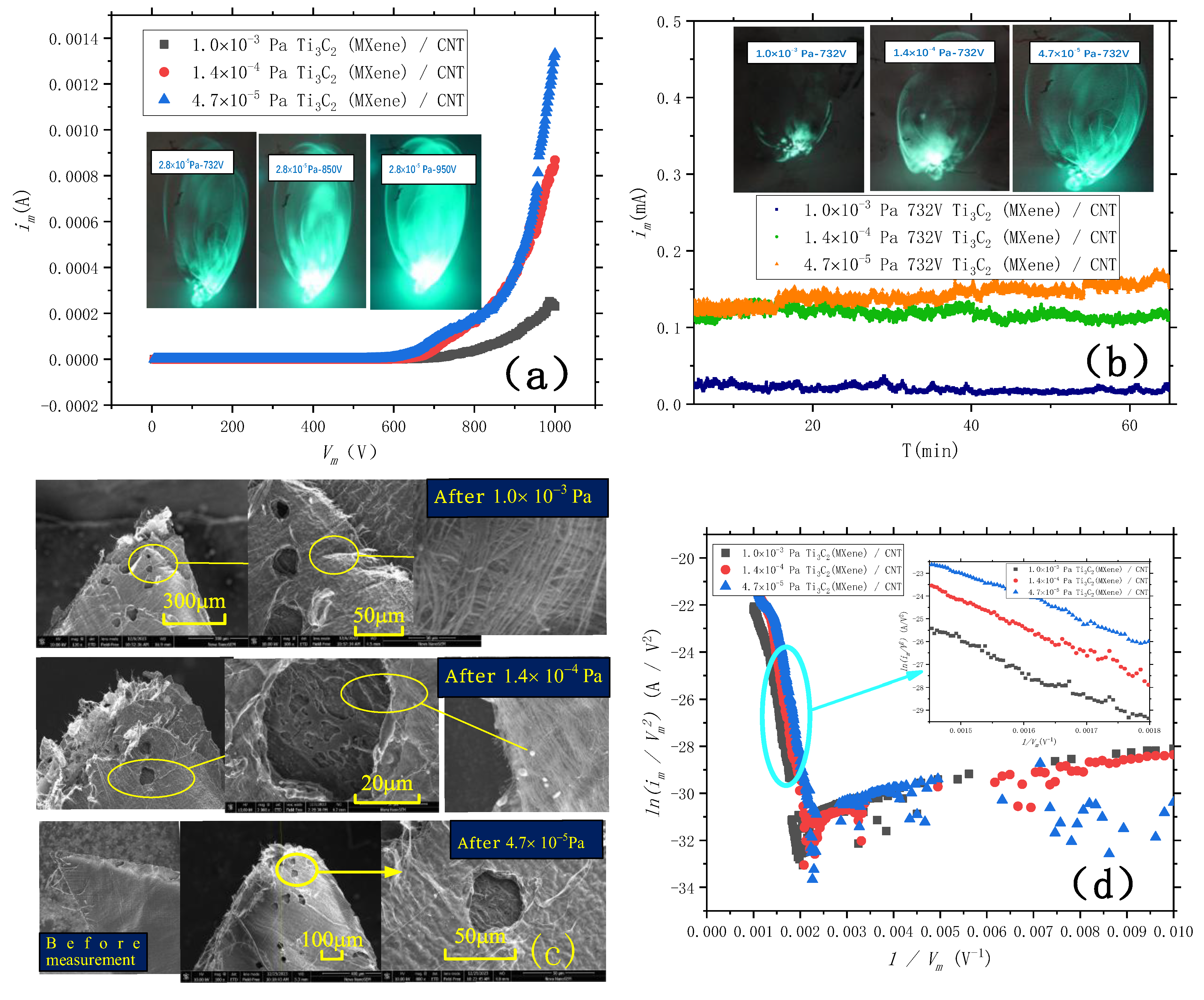
The film sample was subsequently transformed into a curved tip (with a central angle of approximately 45 degrees and a radius of about 10mm), replacing the original square shape. Utilizing tip emission. A fluorescent screen is used as an anode, the distance (d) between the emitting surface and the anode is maintained at around 500 μm. We first tested the change of current with voltage in a low vacuum environment (about 1.0×10⁻³ Pa) and tested the stability, and then following using scanning electron microscopy to measurement the image of the emitted arc tip thin film material, Then increase the vacuum degree and repeat the experiment.
As depicted (Figure 5a,b) the field emission current of Ti3C2 (MXene) / CNT device slightly increases with increasing vacuum degree, this phenomenon is attributed to the effects of vacuum environment on emission stability, current density and lifetime. In low vacuum conditions, ignition, gas ionization and ion bombardment cathode can occur and affect the performance of field emission devices. Conversely, high vacuum environments reduce gas molecule collisions and scattering between electrons and molecules while also decreasing the probability of gas adsorption by the chamber walls. These factors enhance electron emission from cathode materials leading to improved current stability.[17] Foretheremore, the brightness of the screen is also indicative of the size of the electron beam generated through field emission from the cathode material.
The morphological changes observed after each test are depicted (Figure 5c), which shows SEM images of Ti3C2 (MXene) / CNT film. It is evident that as the tests progress towards the tip, the sample experiences more severe damage. Following the initial low vacuum (1.0×10⁻³ Pa) test, significant morphological alterations occurred, particularly at the posterior region of the tip where holes were observed. Additionally, it was apparent that CNT within the surface layer had undergone vaporization, potentially attributed to field emission under low vacuum conditions and thermal effects caused by emitted oxygen leading to carbon vaporization into holes on the surface. However, minimal damage was observed on lower regions due to their coverage by Ti3C2 (MXene ) film. This phenomenon can be explained by Joule-heating resulting from increased temperature, while the local carrier generation promoting that emission simultaneously enhancing. Furthermore, the nanochannels can be limit transportation of generated holes. The source material of the emission has remained relatively unchanged over an extended period of time, primarily due to its ability to inversely suppress net carrier generation and stabilize enhanced current flow. [40] The outermost layer of the material is coated with a CNT film, and the presence of these small holes may be attributed to defects in the crystal structure of the CNTs. Consequently, electron accumulation occurs at these holes place, and leading to an increase in material temperature and subsequent vaporization.
4. Conclusions
The Ti3C2 (MXene) / CNT composite structure exhibits robust mechanical properties and is easily cut, making it suitable for electronic devices in low vacuum. Additionally, it demonstrates excellent field emission properties under low vacuum conditions. After mixing CNT, at an electric field of 2.91 V∙µm−1, current density reached up to 3.49 A.cm-2. It has low turn-on field (Eon) 1.6 V∙μm-1, and low threshold electric field (Eth) 0.22 μA.cm-2. And the field enhancement factor β is 3453, it is about 4.5 times more than pristine Ti3C2 (MXene) (β=750). These materials are suited to fabricate vacuum devices.
The cold electron emission from 2D Ti3C2 (MXene) was comparatively studied with Ti3C2 (MXene) / CNTs nanosheets. Moreover, the field emission current is influenced by various factors, including the vacuum level, aspect ratio of the emission film material, shape of the cathode emission surface, temperature, surface structure of the film, and impedance of the anode phosphor screen. Additionally, it can be considered to modify the band structure of the material through introducing impurity elements, and alter the work function and consequently adjust the emission current. The development of new Ti3C2 (MXene) / CNTs composites also offers us additional possibilities for investigating field emission performance, which will be our next focus.
These films exhibited robust mechanical properties and were easily molded into desired shapes, andalso exhibits superior field emission characteristics in low vacuum conditions, rendering it highly suitable for electronic devices operating under such environments. Additionally, Ti3C2 (MXene) / CNTs composites doped with other elements can also be utilized as pressure sensors and bilateral brakes. Furthermore, since Jianli Wang and his colleagues employed CNT / MXenes nanospheres for the fabrication of lithium-sulfur batteries in 2019, CNT / MXenes have been consistently reported as a promising material for solar cells, Combined with Carbon nanotubes (CNT) can be utilized to fabricate diverse optoelectronic devices that are especially suitable for operation in vacuum environment [43,44,45]. It is anticipated that these films will find potential applications in future research studies.
Author Contributions
The author specially thanks J.X.Wang, J.T.Wang, L.L.Zhang, H.T.Yang, J.J.Sun, and S. S. Fan. He for help during the preparation of the manuscript.
Funding
This work has been financially supported by the National Key Research and Development Program of China (2024 YFA 1210601) from the Ministry of Science and Technology of China.
Conflicts of Interest
The authors declare no conflict of interest.
References
- Lipatov, A.; Alhabeb, M.; Lukatskaya, M. R.; Boson, A.; Gogotsi, Y.; Sinitskii, A. Effect of Synthesis on Quality, Electronic properties and environmental stability of individual monolayer Ti3C2 MXene flakes. Adv. Electron. Mater 2016, 2, 1600255. [Google Scholar] [CrossRef]
- Khan, K.; Tareen, A. K.; Iqbal, M.; Hussain, I.; Mahmood, A.; Khan, U.; Khan, M. F.; Zhang, H.; Xie, Z. J. Recent advances in MXenes: a future of nanotechnologies. J. Mater. Chem. A 2023, 11, 19764–19811. [Google Scholar] [CrossRef]
- Wu, H.; Shen, S. Q.; Xu, X. Y.; Qiao, C. Y.; Chen, X. H.; Li, J.; Li, W. W.; Wei, O. Y. Facile fabrication and high field emission performance of 2-D Ti3C2Tx MXene nanosheets for vacuum electronic devices. IEEE Transactions on Electron Devices 2020, 67, 5138–5143. [Google Scholar] [CrossRef]
- Naguib, M.l; Barsoum, M. W.; Gogotsi, Y. Ten Years of Progress in the Synthesis and Development of MXenes. Adv. Mater. 2021, 33, 2103393. [Google Scholar] [CrossRef] [PubMed]
- She, Z. W.; Fredrickson, K. D.; Anasori, B.; Kibsgaard, J.; Strickler, A. L.; Lukatskaya, M. R.; Gogotsi, Y.; Jaramillo, T. F.; Vojvodic, A. Two-Dimensional Molybdenum Carbide (MXene) as an Efficient Electrocatalyst for Hydrogen Evolution. ACS Energy Lett. 2016, 1, 589−594. [Google Scholar] [CrossRef]
- Kiran, N. U.; Deore, A. B.; More, M. A.; Late, D. J.; Rout, C. S.; Mane, P.; Chakraborty, B.; Besra, L.; Chatterjee, S. Comparative study of cold electron emission from 2D Ti3C2TX MXene nanosheets with respect to its precursor Ti3SiC2 MAXphase. ACS Appl. Electron. Mater. 2022, 4, 2656−2666. [Google Scholar] [CrossRef]
- Hong, X. D.; Zheng, H. R.; Liang, D. Enhanced field emission properties From plasma treated Ti₃C₂Tₓ (MXene) emitters. Mater. Res. Express 2020, 7, 115011. [Google Scholar] [CrossRef]
- Zhan, Y. G.; Lei, L.; Cao, Y. X.; Yang, Y. Y.; Wang, W. J.; Wang, J. F. High-strength, low infrared emission nonmetallic films for highly efficient Joule/solar heating, electromagnetic interference shielding and thermal camouflage. Mater. Horiz 2023, 10, 235–247. [Google Scholar] [CrossRef]
- Ding, W. J.; Liu, P.; Bai, Z. Z.; Wang, Y. Y.; Liu, G. Q.; Jiang, Q. L.; Jiang, F. X.; Liu, P. P.; Liu, C. G.; Xu, J. K. Constructing Layered MXene / CNTs Composite Film with 2D–3D Sandwich Structure for High Thermoelectric Performance. Adv. Mater. Interfaces 2020, 7, 2001340. [Google Scholar] [CrossRef]
- Xu, M. Y.; Liang, L.; Qi, J.; Wu, T. L.; Zhou, D.; Xiao, Z. B. Intralayered Ostwald Ripening-Induced Self-Catalyzed Growth of CNTs on MXene for Robust Lithium–Sulfur Batteries. Small 2021, 17, 2007446. [Google Scholar] [CrossRef]
- Wan, S.J.; Li, X.; Chen, Y.; Liu, N.; Du, Y.; Dou, S.X.; Jiang, L.; Cheng, Q. F. High-strength scalable MXene films through bridging-induced densification. Science 2021, 374, 96–99. [Google Scholar] [CrossRef]
- Weng, G.M.; Li, J. Y.; Mohamed Alhabeb; Christopher Karpovich; Wang H; Jason Lipton; KathleenMaleski; Jaemin Kong; Evyatar Shaulsky; Menachem Elimelech; Yury Gogotsi; André D. Taylor Layer-by-Layer Assembly of Cross-Functional Semi-transparent MXene-Carbon Nanotubes Composite Films for Next-Generation Electromagnetic Interference Shielding. Adv. Funct. Mater. 2018, 28, 1803360. [CrossRef]
- Wu, H.; Zhu, C. B.; Li, X. L.; Hu, X. P.; Xie, H.; Lu, X.; Qu, J.P. Layer-by-layer assembly of multifunctional NR / MXene / CNTs composite films with exceptional electromagnetic interference shielding performances and excellent mechanical properties. Macromol. Rapid Commun. 2022, 43, 2200387. [Google Scholar] [CrossRef]
- Aamir Iqbal; Pradeep Sambyal; Chong Min Koo 2D MXenes for electromagnetic shielding: A Review. Adv. Funct. Mater. 2020, 30, 2000883. [CrossRef]
- Wu, F. S.; Hu, P. Y.; Hu, F. Y.; Tian, Z. H.; Tang, J. W.; Zhang, P. G.; Pan, L.; Michel W. Barsoum; Cai, L. Z.; Sun, Z. M. Multifunctional MXene / C aerogels for enhanced microwave absorption and thermal insulation. Nano-Micro Lett. 2023, 15, 194. [Google Scholar] [CrossRef]
- Lee, J. S.; You, K. H.; Park, C. B.; Photoactive, H. Low bandgap TiO2 nanoparticles wrapped by graphene. Adv. Mater. 2012, 24, 1084–1088. [Google Scholar] [CrossRef]
- Liu, P. Super-aligned carbon nanotube neutralizers for aerospace. nature reviews electrical engineering 2024, 1, 73–74. [Google Scholar] [CrossRef]
- Evtukh, A.; Hartnagel, H.; Yilmazoglu, O.; Mimura, H.; Pavlidis, Band Bending and Work Function.D. Vacuum nanoelectronic devices: novel electron sources and applications; John Wiley & Sons: Chennai, India, 2015;PP.105-107.
- Chen, J. T.; Yang, B. G.; Lim, Y. D.; Duan, W. H.; Zhao, Y.; Tay, B. K.; Yan, X. B. Ti3C2 (MXene) based field electron emitters. Nanotechnology 2020, 31, 285701. [Google Scholar] [CrossRef]
- Yang, B. G.; Chen, J. T.; Wu, X. N.; Liu, B.; Liu, L. Y.; Tang, Y.; Yan, X. B. Enhanced field emission performance of MXene–TiO2 composite films. Nanoscale 2021, 13, 7622–7629. [Google Scholar] [CrossRef] [PubMed]
- Alhabeb, M.; Maleski, K.; Anasori, B.; Lelyukh, P.; Clark, L.; Sin, Saleesha; Gogotsi, Y. Guidelines for Synthesis and processing of two-dimensional titanium carbide ( Ti3C2Tx MXene ). Chem. Mater. 2017, 29, 7633−7644. [Google Scholar] [CrossRef]
- Naguib, M.; Kurtoglu, M.; Presser, V.; Lu, J.; Niu, J. J.; Min, H; Hultman, L.; Gogotsi, Y.; Barsoum, M. W. Two-dimensional nanocrystals produced by exfoliation of Ti 3 AlC 2. Adv. Mater. 2011, 23, 4248–4253. [Google Scholar] [CrossRef]
- Shahzad, F.; Alhabeb, M; Hatter, C. B.; Anasori, B.; Hong, S. M.; Koo, C. M.; Gogotsi, Y. Electromagnetic interference shielding with 2D transition metal carbides ( MXenes ). Science 2016, 353, 1137–1140. [Google Scholar] [CrossRef]
- Yu, W.; Liu, C. H.; Fan, S. S. Advances of CNT-based systems in thermal management. Nano Res. 2021, 14, 2471–2490. [Google Scholar] [CrossRef]
- Jiang, K. L.; Wang, J. P.; Li, Q. Q.; Liu, L.; Liu, C. H.; Fan, S. S. Superaligned carbon nanotube arrays, films, and yarns: a road to applications. Adv. Mater. 2011, 23, 1154–1161. [Google Scholar] [CrossRef]
- Wang, Y. F.; Liang, L. Y.; Du, Z. R.; Wang, Y. M.; Liu, C. T.; Shen, C. Y. Biodegradable PLA / CNTs / Ti3C2Tx MXene nanocomposites for efficient electromagnetic interference shielding. J Mater Sci: Mater Electron 2021, 32, 25952–25962. [Google Scholar] [CrossRef]
- Lai, S. H.; Chang, K. L.; Shih, H. C.; Huang, K. P.; Lin, P. Electron field emission from various morphologies of fluorinated amorphous carbon nanostructures. Appl. Phys. Lett. 2004, 85, 6248–6250. [Google Scholar] [CrossRef]
- Qiao, C. Y.; Wu, H.; Xu, X.; Guan, Z. X.; Ou-Yang, W. Electrical conductivity enhancement and electronic applications of 2D Ti3C2Tx MXene materials. Adv. Mater. Interfaces 2021, 8, 2100903. [Google Scholar] [CrossRef]
- Pandey, A.; Prasad, A.; Moscatello, J. P.; Engelhard, M; Wang, C. M.; Yap, Y. K. Very stable electron field emission from strontium titanate coated carbon nanotube matrices with low emission thresholds. Pandeyetal 2013, 7, 117–125. [Google Scholar] [CrossRef]
- De Rose, L. B.; Catanzaro, D. H.; Choi, C.; Scherer, A. Effect of praseodymium coating on electron emission from a nanoscale gold field emitter array. J. Vac. Sci. Technol. B 2023, 41, 042801. [Google Scholar] [CrossRef]
- Kuttel, O.M.; Groning, O.; Emmenegger, C.; Nilsson, L.; Maillard, E.; Diederich, L.; Schlapbach, L. Enhanced field emission from a carbon nanotube array coated with a hexagonal boron nitride thin film. small 2015, 11, 3710–3716. [Google Scholar]
- Schultz, T.; Frey, N.C.; Hantanasirisaku, K.; Park, S.; May, S. J.; Shenoy, V. B.; Gogotsi, Y.; Koch, N. Surface Termination Dependent Work Function and Electronic Properties of Ti3C2Tx MXene. Chem. Mater. 2019, 31, 6590−6597. [Google Scholar] [CrossRef]
- Ahmed, S. F.; Moon, M. W.; Lee, K. R. Enhancement of electron field emission property with silver incorporation into diamondlike carbon matrix. Appl. Phys. Lett. 2008, 92, 193502. [Google Scholar] [CrossRef]
- Jonge, N. D.; Allioux, M.; Doytcheva, M.; Kaiser, M.; Teo, K. B. K.; Lacerda, R. G.; Milne, W. I. Characterization of the field emission properties of individual thin carbon nanotubes. Appl. Phys. Lett. 2004, 85, 1607–1609. [Google Scholar] [CrossRef]
- Wu, Y. H.; Li, J.; Ye, J. C.; Song, Y. J.; Chen, X. H.; Huang, S. M.; Sun, Z.; Wei, O. Y. Outstanding field emission properties of titanium dioxide / carbon nanotube composite cathodes on 3D nickel foam. Journal of Alloys and Compounds 2017, 726, 675–679. [Google Scholar] [CrossRef]
- Forbes, R. G. Field emission: Applying the “magic emitter” validity test to a recent paper, and related research-literature integrity issues. J. Vac. Sci. Technol. B 2023, 41, 042807. [Google Scholar] [CrossRef]
- Mahajan, A; Khan, N.; Yadav, K. K.; Jha, M.; Ghosh, S. Efficient field emission from ultrafine nanostructured lanthanum sulfide synthesized by chemical route. App. Sur. Sci. 2023, 623, 156996. [Google Scholar] [CrossRef]
- Limbu, T. B.; Chitara, B.; Orlando, J. D.; Garcia Cervantes, M. Y.; Kumari, S.; Li, Q.; Tang, Y. G.; Yan, F. Green synthesis of reduced Ti3C2Tx MXene nanosheets with enhanced conductivity, oxidation stability, and SERS activity. J. Mater. Chem. C 2020, 8, 4722–4731. [Google Scholar] [CrossRef]
- Ahmed, sk. F.; Ghosh, P. K.; khan, S.; Mitra, M. K.; Chattopadhyay, K. K. Low-macroscopic field emission from nanocrystalline Al doped SnO2 thin films synthesized by sol–gel technique. Appl. Phys. A 2007, 86, 139–143. [Google Scholar] [CrossRef]
- Huang, Y. F.; Chen, Y.; Huang, Z. J.; Zeng, M. X.; Gu, Z. G.; Yang, W.; Chen, J. P-type Si-Tips with integrated nanochannels for stable nonsaturated high current density field electron emission. Personal use is permitted, but republication/redistribution requires IEEE permission. Ieee transactions on electron devices 2022, 69, 7, 3908-3913. [Google Scholar] [CrossRef]
- Hong, X. D.; Zheng, H. R.; Liang, D. Enhanced field emission properties from plasma treated Ti3C2Tx (MXene) emitters. Mater. Res. Express 2020, 7, 115011. [Google Scholar] [CrossRef]
- Forbes, R. G.; Deane, J. H. B. Reformulation of the standard theory of Fowler–Nordheim tunnelling and cold field electron emission. Proc. R. Soc., Ser. A 2007, 463, 2907–2927. [Google Scholar] [CrossRef]
- Li, H. Q.; Wu, Z.; Xing, Y, Q.; Li, B. G.; Liu, L. Photoelectric synergistic response properties of the Ti3C2Tx MXene - CNT / PDMS bilayer actuator. Nano Energy 2022, 103, 107821. [Google Scholar] [CrossRef]
- Wang, J. L.; Zhang, Z.; Yan, X. F.; Zhang, S. L.; Wu, Z. H.; Zhuang, Z. H.; Han, W. Q. Rational design of porous N-Ti3C2 MXene / CNT microspheres for high cycling stability in Li–S battery. Nano-Micro Lett. 2020, 12, 4. [Google Scholar] [CrossRef]
- Agresti, A.; Pazniak, A.; Pescetelli, S.; Vito, A. Di.; Rossi, D.; Pecchia, A.; Auf der Maur, M.; Liedl, A.; Larciprete, R.; Kuznetsov, D.V.; D. Saranin; Carlo, A. Di. Titanium-carbide MXenes for work function and interface engineering in perovskite solar cells. Nat. Mater. 2019, 18, 1228–1234. [CrossRef] [PubMed]
- Zhang, P. C.; Ru, X. H.; Li, H. Y.; Liang, H. Y.; Wang, H. P.; Yang, C. H.; Zhang, X. G.; Liu, Z. G.; Zhang, Q. Y.; Chen, Y. H. Efficient MXene / CNT electromagnetic shielding composite films with self-assembly multilayer structure. J Mater Sci Mater Electron 2023, 34, 39. [Google Scholar] [CrossRef]
Figure 1.
Schematic diagram for the fabrication of multilayer film Ti3C2 (MXene)/CNT.
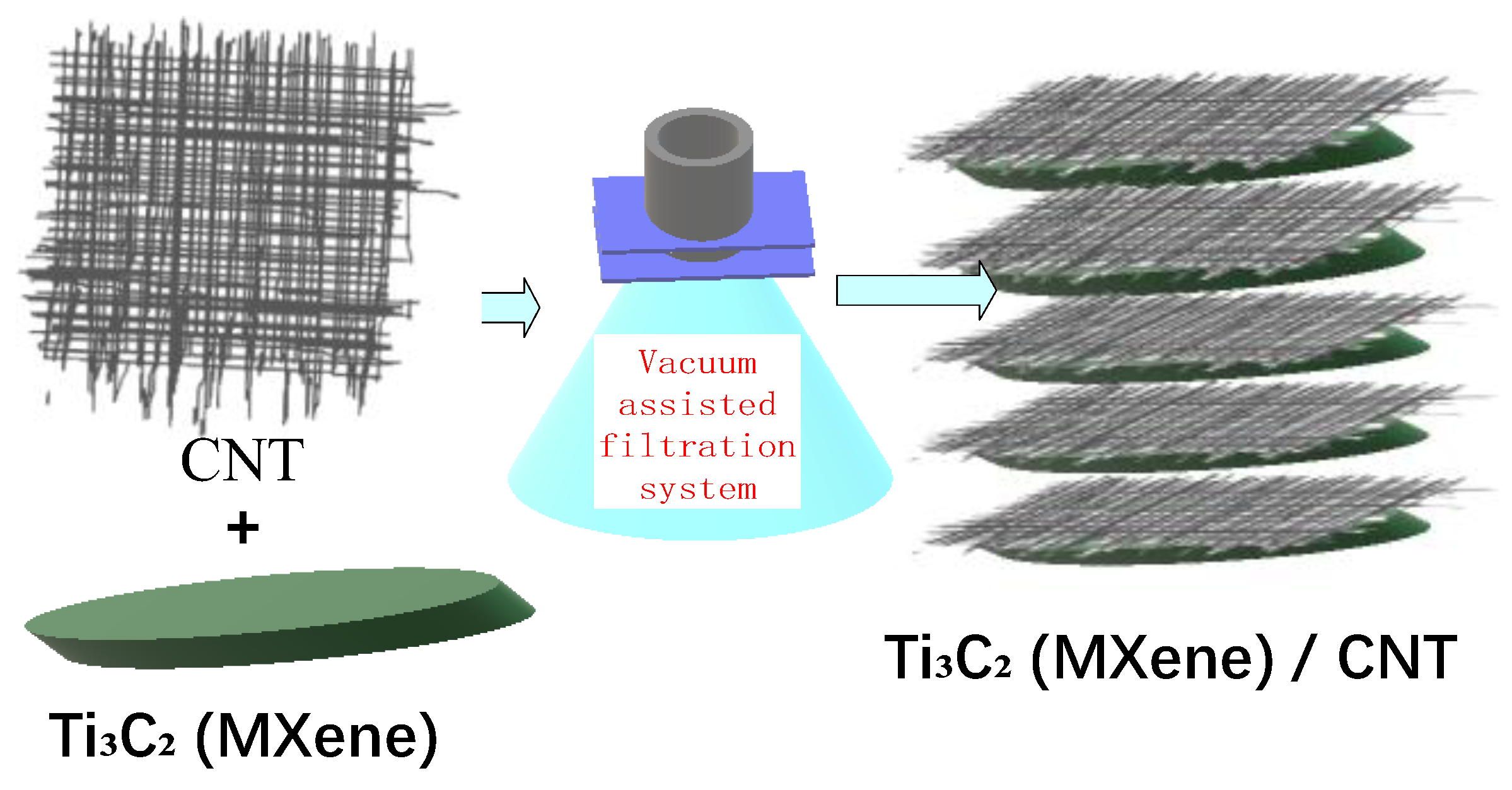
Figure 2.
The SEM images of pristine Ti3C2(MXene) film(a,b)and Ti3C2(MXene) / CNT film(c,d)the stress–strain curves of Ti3C2(MXene) / CNT(e).
Figure 2.
The SEM images of pristine Ti3C2(MXene) film(a,b)and Ti3C2(MXene) / CNT film(c,d)the stress–strain curves of Ti3C2(MXene) / CNT(e).
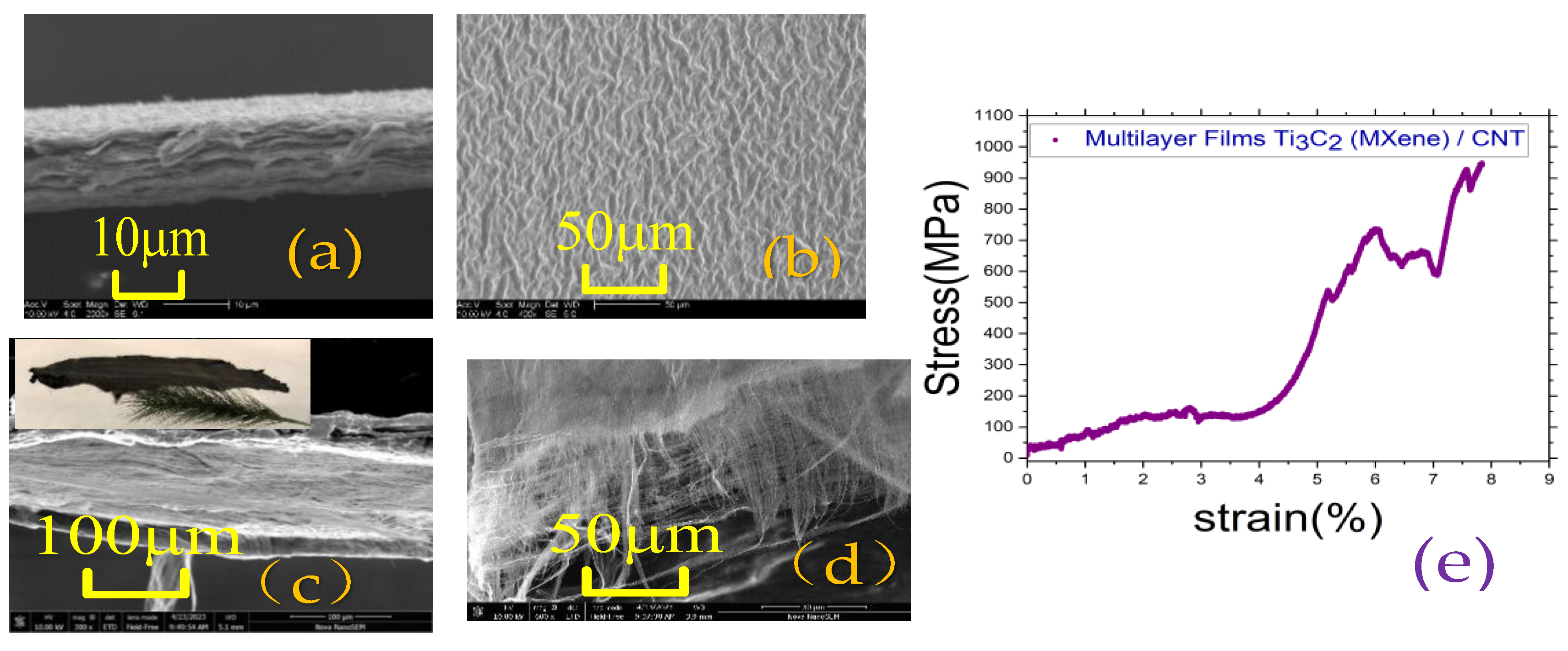
Figure 3.
The J-E curev surround vacuum chamber pressure 3.7×10⁻⁶ Pa and 2.1×10⁻⁵ Pa . (a) The stability (J–t) curve current of field emission under the electric field intensity 6191V/ mm. (b) The typical Fowler-Nordheim plots under different vacuum pressure. (c) The XRD patterns combined with films of Ti3C2 (MXene)and Ti3C2 (MXene) / CNTs. (d).
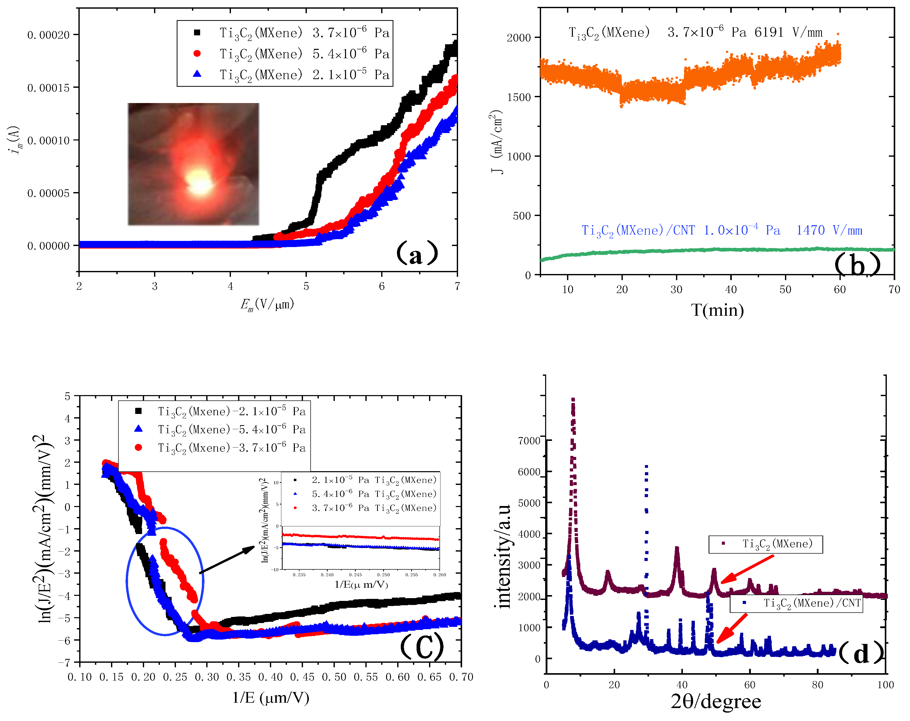
Figure 4.
EDS spectra of Ti3C2 (MXene ) before(a) and after (b) field emission. The J-E curve field emission performance of Ti3C2 (MXene) / CNT, and the surround vacuum pressure 2.4×10⁻⁴ Pa. (c) The typical Fowler-Nordheim plots under different vacuum pressure. (d).
Figure 4.
EDS spectra of Ti3C2 (MXene ) before(a) and after (b) field emission. The J-E curve field emission performance of Ti3C2 (MXene) / CNT, and the surround vacuum pressure 2.4×10⁻⁴ Pa. (c) The typical Fowler-Nordheim plots under different vacuum pressure. (d).
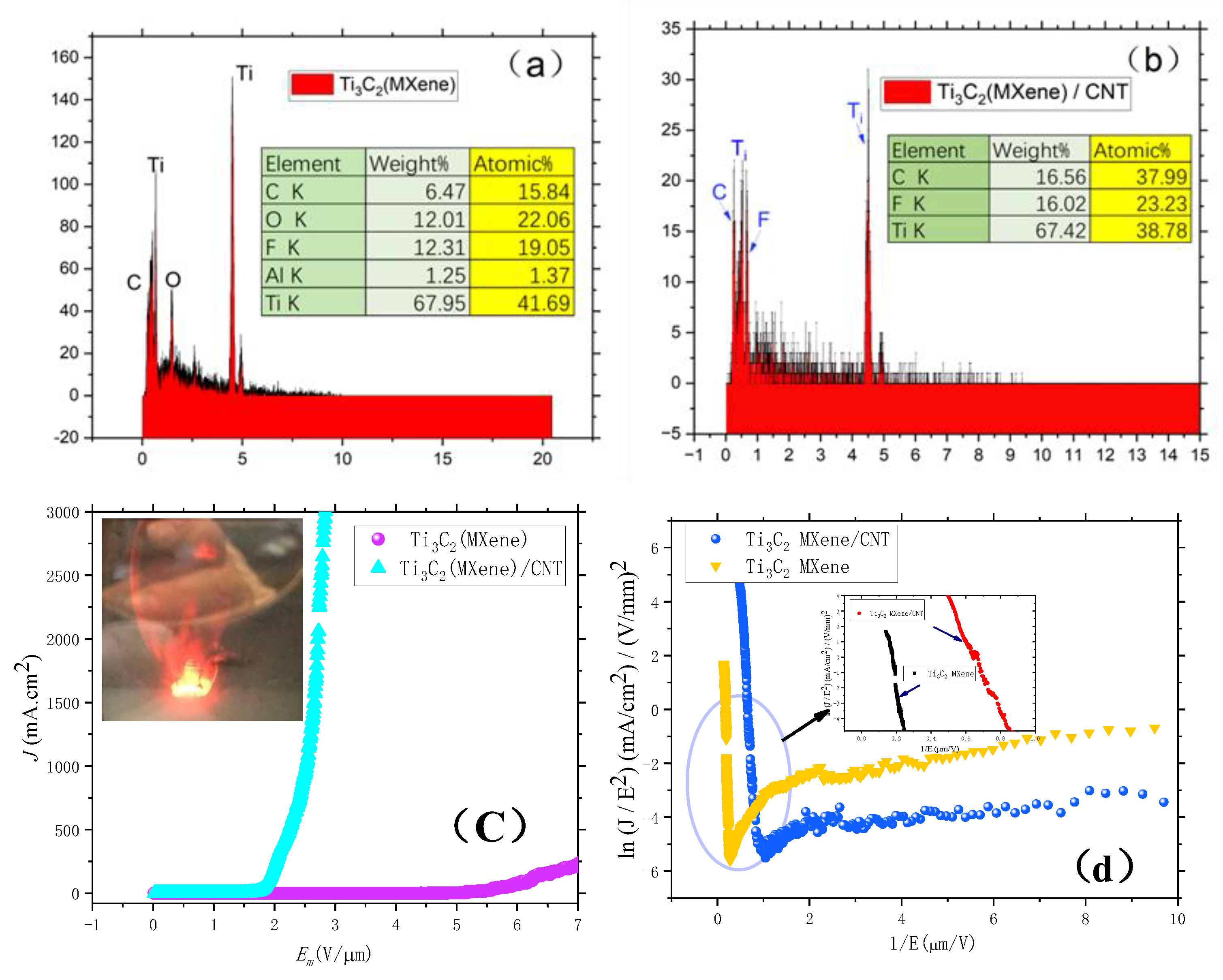
Figure 5.
The I-V curve field emission performance of Ti3C2 (MXene ) / CNT (a) The typical Fowler-Nordheim plots under different vacuum pressure.(b) The SEM images of Ti3C2 (MXene) / CNT film (c). The typical Fowler-Nordheim plots under different vacuum pressure (d).
Figure 5.
The I-V curve field emission performance of Ti3C2 (MXene ) / CNT (a) The typical Fowler-Nordheim plots under different vacuum pressure.(b) The SEM images of Ti3C2 (MXene) / CNT film (c). The typical Fowler-Nordheim plots under different vacuum pressure (d).
Disclaimer/Publisher’s Note: The statements, opinions and data contained in all publications are solely those of the individual author(s) and contributor(s) and not of MDPI and/or the editor(s). MDPI and/or the editor(s) disclaim responsibility for any injury to people or property resulting from any ideas, methods, instructions or products referred to in the content. |
© 2025 by the authors. Licensee MDPI, Basel, Switzerland. This article is an open access article distributed under the terms and conditions of the Creative Commons Attribution (CC BY) license (http://creativecommons.org/licenses/by/4.0/).
Copyright: This open access article is published under a Creative Commons CC BY 4.0 license, which permit the free download, distribution, and reuse, provided that the author and preprint are cited in any reuse.


