
Submitted:
18 December 2025
Posted:
22 December 2025
You are already at the latest version
Abstract
High-precision non-contact online voltage monitoring has attracted considerable attention due to its improved safety. Based upon existing research works and validation of non-contact voltage measurement techniques, an enhanced approach for online voltage monitoring is proposed in this paper. By analyzing the relationship between distributed capacitance and coupling capacitance, a resistive–capacitive signal input circuit is designed to address scenarios involving large distributed capacitance in engineering applications. Furthermore, to improve measurement accuracy, a phase shift vibration method is introduced based on the investigation of the effect of relative phase shifts in mixed-frequency signals. The proposed circuit architecture and data processing method are simple in design and have been verified through experimental prototype, demonstrating stable long-term performance under room-temperature conditions.
Keywords:
non-contact voltage measurement
; RC input circuit
; phase shift vibration method
; stray capacitance
; online monitoring
1. Introduction
Online monitoring of low-voltage signals is widely applied in power systems, rail transportation, and industrial control. In recent years, extensive research works have been conducted on non-contact voltage measurement techniques. Electric field coupling based non-contact voltage measurement methods have been proposed and studied [1,2,3,4,5] which enable safer and more reliable online voltage monitoring. Research works [1,6,7,8,9,10] have verified the feasibility of applying such techniques in transformer voltage detection, power transmission measurement, and partial discharge monitoring. However, conventional electric field coupling based non-contact voltage measurement techniques suffer from significant errors, as the coupling capacitance is affected by factors such as the insulation medium, installation position, and wire diameter of the measured conductor. In practical applications, variations in wire diameter or material between the measured and test cables, shifts in the conductor’s core position, and environmental temperature fluctuations can all cause dynamic changes in coupling capacitance, resulting in substantial measurement deviations. To mitigate these effects, some studies [3,11,12] introduced signal-injection-based non-contact voltage measurement methods grounded in electric field coupling, effectively addressing capacitance variation issues in laboratory conditions. Haberman further analyzed the error sources and noise mechanisms of this approach [13]. Delle et al. enhanced this method by integrating analog filter and peak detection circuits with an MCU for data computation [14], achieving high accuracy. Nevertheless, the resulting circuit remains complex and is incapable of simultaneously measuring additional parameters such as frequency and phase. Moreover, existing studies have rarely addressed engineering scenarios in which distributed capacitance becomes substantially larger than coupling capacitance, such as in systems designed to improve electromagnetic compatibility. In these cases, large distributed capacitance can significantly amplify measurement errors arising from coupling capacitance fluctuations. A promising solution involves discrete sampling and digital filtering combined with RMS computation, which can simplify the circuit while enabling concurrent measurement of voltage amplitude, frequency, and phase. However, in signal-injection methods, the low-frequency drift of the relative phase in the mixed-frequency signal generated by the interaction between the injected and measured signals can degrade measurement accuracy. To overcome these challenges, this paper proposes an improved non-contact voltage measurement method employing a resistive–capacitive input structure. This design mitigates measurement errors caused by minor coupling capacitance variations under large distributed capacitance conditions. By increasing the vibration frequency of the mixed-signal’s relative phase and integrating RMS filtering, the proposed method achieves high measurement accuracy while substantially simplifying the analog circuitry.
2. Research Status
In electric field coupling based voltage measurement, the coupling probe only needs to serve as an electrode capable of collecting electric charge and can take any geometric form. However, simulation results reported in [15] demonstrate that a cylindrical double-layer copper tube structure provides a more stable coupling capacitance compared with other electrode configurations. A schematic diagram of the probe and its equivalent capacitance distribution is presented in Figure 1.
By injecting a high-frequency signal, the coupling capacitance can be monitored in real time. The voltage on the insulated conductor is then determined by comparing the system’s responses to signals at different frequencies, thereby eliminating the influence of coupling capacitance variations. The principle of the equivalent circuit is illustrated in Figure 2.
In the circuit diagram, the first stage functions as an I–V conversion circuit, while the second stage subtracts from to ensure that the subsequent conditioning circuits process only the effective signal associated with the coupling capacitance, thereby preserving a larger dynamic range for signal amplification.
In Figure 2, represents the coupling capacitance between the measured conductor and the sensing layer. Its value is jointly determined by factors such as the insulation medium of the measured line, the feed through position, and the electrode area. The measured signal is transmitted to the operational amplifier through .
denotes the capacitance between the sensing layer and the shielding layer, which theoretically does not affect the measurement results.
corresponds to the input capacitance, including the equivalent distributed capacitance of the sensing layer and its connecting cable loop to the ground, as well as all stray capacitance s to ground along the transmission path. For the measured signal, acts as a load and therefore does not influence the measurement outcome. However, when the in-phase terminal of the operational amplifier is injected with the signal , directly affects the measurement result of the injected signal.
represents the equivalent distributed capacitance of the shielding layer and its connected cable to the ground, which theoretically has no effect on the measurement results.
Let denote the measured voltage and the injected high-frequency signal voltage, with different amplitudes and angular frequencies. According to the circuit superposition theorem,
where K denotes the amplification factor of the differential circuit. The output voltage contains two components with different frequencies, whose RMS values are and , respectively. These RMS values can be obtained through appropriate filtering and computation of . According to Equation 1, we obtain:
Let
From 5, it can be seen that if is extremely small, then , at this point
If the value of is fixed, then under a given injection signal condition, becomes a constant. This constant can be determined by setting the coupling capacitance , i.e. , by injecting only while positioning the sensing probe away from the measured conductor,and subsequently stored as a fixed zero reference in the register [3]. Now
When the injection signal frequency and amplitude remain constant, both Equation 6 and Equation 7 yield values that depend solely on . By simultaneously solving Equation 2 and Equation 6 (or Equation 7), the measured signal voltage can be determined.
or
As shown in Equations 8 and 9, when this method is applied to measure , its value remains independent of , thereby effectively eliminating measurement errors caused by variations or uncertainties in the coupling capacitance.
2.1. Existing Issues
Analysis of Equations 8 and 9 indicates that although the calculation formula for is not directly dependent on , Equations 2 and 4 reveal that both and are influenced by . In addition, is also affected by the input capacitance . Previous studies generally assume that is sufficiently small to be neglected when high measurement accuracy is not required, and this assumption has yielded satisfactory results under laboratory conditions. This conclusion is valid when considering only the discrete ground capacitance of the sensing probe and its connecting wires. However, when the non-contact voltage measurement method is applied to the low-voltage online monitoring scenarios discussed in this paper, the actual value of can become considerably larger due to the complex electromagnetic environment at engineering sites. To improve electromagnetic compatibility, multi-layer printed circuit boards with dedicated power and ground planes are typically used, which substantially increase the value of in the signal input path. As a result, may reach several times—or even exceed—the coupling capacitance , and it is affected by factors such as the relative positions of the probe and measured cable,Input capacitance of the operational amplifier in the circuit, PCB layout, and substrate material. Consequently, cannot be ignored and exerts a significant impact on the measurement results. Reference [16] proposed a self-calibration technique based on switch-controlled parameter correction, which eliminates the effect of by solving simultaneous equations. However, this approach overlooks the capacitance introduced by the switches themselves and the dynamic variations in coupling capacitance during switching, making it unsuitable for field engineering applications. Similarly, Reference [3] experimentally demonstrated that, for high-precision measurements, calibrating and storing when it acts solely on (denoted as ) provides a direct and convenient method to compensate for its influence. Nevertheless, re-examining Equation 2 reveals that results from the combined effects of acting on both and . When is excessively large, small variations in —caused, for instance, by minor cable displacement or temperature fluctuations—may become indistinguishable, leading to substantial measurement deviations.
For example, consider (estimated using the capacitance definition formula) and (an approximate value dependent on PCB layout an innput capacitance of the operational amplifier). If varies slightly by (i.e., ) due to cable movement, the resulting change in the measured voltage can be significant.
It is evident that as the distributed capacitance increases further, the value in Equation 11 decreases correspondingly. In the circuit, this phenomenon manifests as a pronounced change in , while the variation in remains minimal or cannot be accurately detected, ultimately resulting in substantial measurement errors when using Equation 8 or 9.
2.2. Proposed Solution
To address this problem, this paper proposes a non-contact online voltage monitoring method based on resistive–capacitive coupling. The method introduces a resistive–capacitive input structure to suppress the influence of distributed capacitance and enhance sensitivity to variations in the coupling capacitance. As a result, the proposed approach maintains high measurement accuracy even under minor dynamic changes in coupling capacitance during long-term operation. Another challenge identified from Equations 8 and 9 is that when the denominator term is small, even slight fluctuations can lead to large deviations in the calculated measurement results. Considering limitations imposed by circuit configuration, insulation, and electromagnetic radiation, the amplitude of is typically constrained and cannot be set excessively high. Therefore, the excitation frequency must be maximized within the permissible bandwidth. However, this often produces situations in which the denominator magnitude is considerably smaller than that of the numerator, making the measurement results highly sensitive to minor perturbations in .
Moreover, under the signal injection scheme, becomes a mixed-frequency signal composed of and , which originate from independent and uncorrelated sources. Relative phase shifts inevitably occur during signal transmission [17], and when the mixed signal is digitized using a common reference clock, sampling drift can further induce fluctuations in the computed results. Additionally, the parasitic capacitance in the transmission path may amplify the effect of phase shifts, requiring careful consideration in subsequent data processing to achieve high-precision measurement.
To overcome this limitation, this study conducts an in-depth analysis of the fluctuation mechanism and proposes increasing the relative phase vibration frequency of the mixed-frequency signal by optimizing the injected signal frequency. This strategy enables effective digital filtering, eliminates data fluctuations caused by phase drift, and achieves high-precision online monitoring with a simplified circuit structure.
3. Circuit Principles
In current engineering applications, online voltage monitoring devices predominantly employ micro controller units (MCU) as processing cores. Digital signal processing techniques are used to replace complex analog circuits and eliminate the need for computers in large-scale raw data processing. Measurement results are typically transmitted via a field bus interface. The verification circuit designed in this study adopts the same architecture to validate the proposed methodology.
Following the recommendation of ShenilP. et al. [12], the voltage sensing probe is implemented using a double-layer copper tube structure, as illustrated in Figure 1. The outer layer, with a diameter of 11 mm and a length of 40 mm, serves as the shielding layer, while the inner layer, with a diameter of 6 mm and a length of 4 mm, functions as the sensing electrode. The probe is connected to the conditioning circuit through a shielded cable to minimize interference and maintain signal integrity.
3.1. Resistive-Capacitive Signal Input Circuit
To minimize the influence of large distributed capacitance on the measurement results, this study introduces a resistive–capacitive signal input circuit. The proposed design effectively divides the distributed capacitance within the signal input loop into two distinct components, thereby reducing its impact on overall measurement accuracy. The schematic diagram of the circuit is shown below:
The resistor is integrated into the signal input loop, and its resistance value must be carefully selected. If the resistance is too high, the effective signal entering the subsequent processing circuit will be excessively attenuated; conversely, if it is too low, the resistor will fail to perform its intended function. Based on existing studies and experimental validation, the influence of becomes nearly negligible after adopting the proposed resistive–capacitive input configuration. Consequently, the equivalent circuit shown in Figure 3 can be further simplified, as illustrated in the following diagram:
At this point,
s According to the circuit configuration, when , the branch containing and can be regarded as an open circuit with respect to . Consequently, the measured value depends solely on , forming the term in Equation 5. By appropriately selecting the parameters and such that , the algorithmic principles described in Chapter 2 remain valid for the improved resistive–capacitive input circuit. Moreover, the introduction of effectively alleviates the original problem in which exhibited weak sensitivity to variations in caused by a large , since the effective input capacitance is now reduced to .
4. Data Processing Methods
According to Equation 8, filters must be designed to separately extract and from . As discussed earlier, the proposed method involves division operations with a relatively small denominator, thereby imposing stringent requirements on data stability. During data processing, in addition to conventional factors such as sampling rate, response time, and pass band error, particular attention must be given to phase drift in the mixed-frequency signal during transmission, as it can induce significant fluctuations in the measured data.
4.1. Causes of Data Fluctuations Due to Phase Drift in Mixed-Frequency Signals
In the non-contact voltage monitoring method proposed in this paper, a signal must be injected to enable real-time monitoring of the coupling capacitance. Consequently, the measured signal is superimposed with the injection signal and transmitted to the subsequent conditioning and processing circuits as a mixed-frequency signal for amplification, analog-to-digital (AD) sampling, and computation. To more intuitively illustrate the data fluctuation issue caused by phase drift in the mixed-frequency signal, let and denote the measured signal and the injected signal , respectively.
where and denote the frequencies of the measured and injected signals, respectively, both of which may exhibit slight deviations. represents the phase of each signal. In practical systems, since and originate from independent signal sources, their phase variations, and , are uncorrelated. As a result, the mixed-frequency signal exhibits the characteristics of a non-stationary signal.
where denotes the initial phase of the signal, and represents the deviation of the signal frequency from its ideal value (typically less than 1 Hz when using high-precision signal sources).
As illustrated in Figure 4, the signal after the first-stage operational amplifier is a mixed-frequency signal generated by the aliasing of and . This signal is subsequently passed through a series of linear conditioning circuits for amplification, filtering, and other processing, ultimately producing , which is then subjected to analog-to-digital conversion and computational analysis.
where and denote the amplitudes of the two frequency components in the mixed-frequency signal after passing through the analog channel, while and represent the phase delays introduced by the channel capacitance, which can be regarded as constant for simplified analysis.
Since the system is linear, the phases of the two signals at different frequencies remain relatively independent, and their relative phase drift can be expressed as:
Simplification yields:
When the circuit structure is fixed, C can be considered a constant. However, in the circuit discussed in this paper, since the coupling capacitance may vary, C is not strictly constant. For the sake of simplified analysis, it is treated as a constant in this discussion. At this stage, is fed into the ADC for conversion into a discrete signal, followed by digital computation. Assuming the sampling period is and the number of sampling points per cycle is n, can then be discretized as follows:
For further analysis, by treating as the reference signal, it follows that and . When the frequency settings of the measured and injected signals remain constant, is an extremely small quantity (typically less than 1 Hz when using high-precision signal sources) and is not fixed, as it primarily depends on the relative frequency drift between the two signal sources. At this point,
It can be observed that, after the mixed-frequency signal is discretion, the presence of relative phase drift introduces a sampling-sliding effect, which ultimately leads to fluctuations in the measurement results at the frequency corresponding to . According to Equation 24, if the injected signal is an integer harmonic of the measured signal, i.e., , then becomes a constant. Otherwise, it appears as a time-varying term whose fluctuation frequency depends on the deviation of from . Therefore, the fluctuation frequency of can be analyzed using the following expression:
When , the frequency of is determined by
This indicates that the relative phase drifts at an extremely low frequency. Due to the sampling-sliding effect, the RMS measurement results fluctuate correspondingly at this same frequency. Moreover, when the value of C in Equation 21 approaches or , the amplitude of these fluctuations becomes more pronounced. Figure 5 illustrates the waveform of the mixed-frequency signal at the ADC input when . It can be observed that the waveforms in sub figures (a) and (b) exhibit consistent phase alignment within each sub figure, yet a significant phase shift exists between them. In practice, experimental observations reveal that the phase variation is nearly imperceptible within a single oscilloscope sweep, but becomes clearly noticeable during long-term dynamic monitoring, thereby confirming the presence of phase drift with a relatively long drift period.
At this stage, the input mixed-frequency signal is subjected to discrete sampling and digital filtering, followed by RMS computation to obtain the measured voltage value. Figure 5 presents the measurement results when the target signal is 500 V at 2000 Hz, and the injected signal frequency is 8000 Hz. A total of 150 RMS samples were continuously acquired at a rate of one value per second. Apart from calibration, no additional data processing was applied following the internal computation.
As illustrated in Figure 6, the experimental data exhibit distinct fluctuations within an approximate range of [-1%, 1%], characterized by a relatively low fluctuation frequency. Although the amplitude of these variations appears small, they nonetheless represent a substantial deviation from the 0.2-class accuracy standard currently achievable by contact-type voltage monitoring systems. Furthermore, such low-frequency fluctuations are particularly difficult to suppress using conventional digital filtering techniques. This phenomenon cannot be attributed to spectral leakage or deficiencies in filter design. Control experiments conducted with and confirmed that individual signal inputs do not induce leakage into other frequency bands, and that RMS computations for single-frequency signals maintain excellent accuracy and linearity. However, when mixed-frequency signals are applied, the fluctuation phenomenon observed in Figure 6 emerges. Analysis of MCU memory data reveals that these fluctuations primarily stem from slight oscillations in when . Although the amplitude of these oscillations is negligible relative to the RMS value of itself, Equations 7 and 9 indicate that the final computation of depends solely on the residual component of after subtracting —specifically, the value generated by acting on the coupling capacitance . When , the magnitude of becomes exceedingly small, rendering the calculation of highly sensitive to even minor fluctuations in , thereby resulting in pronounced oscillations in the computed results.
4.2. Solution to Data Fluctuations
Based on the foregoing analysis, although the two frequency components of the mixed-frequency signal are inherently incoherent, they propagate through the same channel into the ADC stage and share a common sampling reference clock, rendering the relative phase drift unavoidable. One potential solution is to employ analog filter circuits in combination with peak detection circuits to separately extract the amplitudes of the two signals before feeding them into the MCU for subsequent subtraction and division operations [14]. However, this approach makes it difficult to simultaneously obtain key parameters essential for online monitoring, such as frequency and phase. Moreover, it substantially increases circuit complexity, leading to higher implementation costs and reduced system reliability—factors that are particularly critical for large-scale engineering deployments. According to Equation 27, this paper proposes a method to increase the vibration frequency of the relative phase. By deliberately introducing a small frequency offset between the injected signal and the harmonic points of the measured signal, the fluctuation frequency of is shifted to a higher range. When combined with digital filtering algorithms, this approach effectively suppresses low-frequency drift and enhances the stability of the measurement results. The proposed implementation is both conceptually simple and practical, significantly reducing overall circuit complexity while maintaining high measurement accuracy. For instance, when the measured signal frequency is and the injection signal frequency is set to , Equation 27 indicates that the RMS value of will exhibit extremely low-frequency fluctuations (typically ). However, if the injection frequency is adjusted to , the fluctuation frequency of the RMS value increases significantly, as expressed by
Fluctuations at this frequency can be readily attenuated using standard digital filtering techniques, thereby improving data stability and measurement precision.
The waveform of the mixed-frequency signal measured at the ADC input port under this non-integer harmonic injection condition is shown in Figure 7. As observed, the mixed-frequency signal exhibits a more pronounced phase drift, with a variation frequency of , consistent with theoretical
Applying the same data processing method used in Figure 6, the corresponding measurement results are presented in Figure 8.
From Figure 8, it can be observed that the stability of the improved data has been significantly enhanced, with the overall fluctuation range reduced to within 0.3%. This demonstrates the effectiveness of the proposed frequency deviation strategy in suppressing low-frequency oscillations and improving measurement consistency.
5. Determination of Circuit Parameters
5.1. Selection of Injection Signal
The frequency selection strategy for has been comprehensively discussed in the preceding chapter. According to [13], when , the capacitive reactance of the coupling capacitance between the sensing and shielding layers can no longer be neglected, and the virtual short assumption of the operational amplifier becomes invalid. As described in Chapter 2, although an excessively high frequency should be avoided, increasing the amplitude of is generally beneficial. Literature [14] suggests that the optimal condition is achieved when . However, as observed from the circuit schematic, the output of the first-stage operational amplifier, , contains a component. Therefore, when determining the amplitude of , it is essential to ensure compatibility between and the power supply voltage of the operational amplifier.
Furthermore, since is an internally injected signal, an excessively high amplitude may cause insulation degradation and induce electromagnetic interference on the measured signal through capacitive coupling. Considering these factors, this study conducted experiments on measured signals with frequencies of 50 Hz (500 V) and 2000 Hz (300 V). A DDS-based signal generation circuit—comprising an AD9833 digital signal generator and a digitally controlled potentiometer—was used to produce a sinusoidal AC signal with adjustable amplitude and frequency. For the 50 Hz test signal, injection frequencies of 2000 Hz and 1970 Hz were compared, while for the 2000 Hz signal, 8000 Hz and 8500 Hz were used. The amplitude of was adjusted such that the magnitudes of and in were approximately equal.
In the improved circuit proposed in this study, parameter determination must account for the input voltage range of the backend MCU to ensure distortion-free signal transmission throughout the entire signal chain. The STM32H7V7X6 micro controller was selected as the processing unit, implementing real-time monitoring for both 50 Hz and 2000 Hz signals using the following workflow: mixed-signal AC sampling → digital filtering → single-frequency RMS computation → algorithmic processing → bus communication output. The RMS values of the filtered signals were obtained using a “two-point multiplication plus low-pass filtering” method. The built-in general-purpose ADC of the STM32H7V7X6 accepts input signals within a 0–3.3 V range. To prevent the “floating ground” phenomenon caused by long signal loops, voltage measurements were taken at both the positive and negative terminals of the measured signal loop, with the true differential voltage obtained through a precision differential circuit. Circuit parameters were determined using a back-calculation approach, and the coupling capacitance was estimated based on the dielectric constant of commonly used cable materials. To ensure broad applicability and prevent data overflow during cable replacement, the coupling capacitance was set to 5 pf. The distributed capacitance on the experimental prototype PCB was measured using an impedance bridge and found to be approximately 10 pf. When determining the key circuit parameters, the following design constraints must be satisfied:
- According to standard engineering practice, a 20% safety margin should be reserved for the MCU input signal range. To simplify the hardware architecture, AC coupling is adopted for sampling. Consequently, the voltage at the ADC input must satisfy the following condition:
- To simplify the circuit design and enhance reliability in engineering applications, the number of distinct power supply voltage levels for all electronic components should be minimized while still satisfying the operating requirements of standard industrial devices. In this design, the operational amplifiers along the signal path are powered by a 12 V supply, the MCU operates at 3.3 V, and the DC bias voltage is set to 1.65 V.
- At each stage of the operational amplifier circuits, the signal peak values must not exceed the corresponding supply voltage limits of the integrated amplifiers. In the improved circuit proposed in this paper, the stages most prone to exceeding these limits are the first-stage current-to-voltage (I–V) conversion circuit and the second-stage subtraction circuit, as both stages handle the full amplitude of . Constrained by the frequency selection principles discussed in Chapter 3, the amplitude of should be as high as possible within the permissible range. As a result, the component appearing at the output of the first-stage I–V conversion circuit is substantially greater than the corresponding values of and .
By substituting the relevant device parameters obtained from the three constraint conditions above into Equations 12 and 13, the prototype circuit parameters for this design can be determined. For the measured signal with a frequency of 50 Hz and an amplitude range of 0–500 V, the main circuit parameters are selected as follows:

Table 1.
Parameter table when the measured signal is 50 Hz.
| (V) | 1 | |||
|---|---|---|---|---|
| 7 | 2000 | 100k | 1M | 10 |
| 7 | 1970 | 100k | 1M | 10 |
1 is the gain of the conditioning circuit between and .
The main circuit parameters selected for the 2000 Hz signal test are as follows:
Table 2.
Parameter table when the measured signal is 2000 Hz.
| (V) | 1 | |||
|---|---|---|---|---|
| 4 | 8000 | 40k | 1M | 10 |
| 4 | 8500 | 40k | 1M | 10 |
1 is the gain of the conditioning circuit between and .
6. Results
6.1. Test Conditions
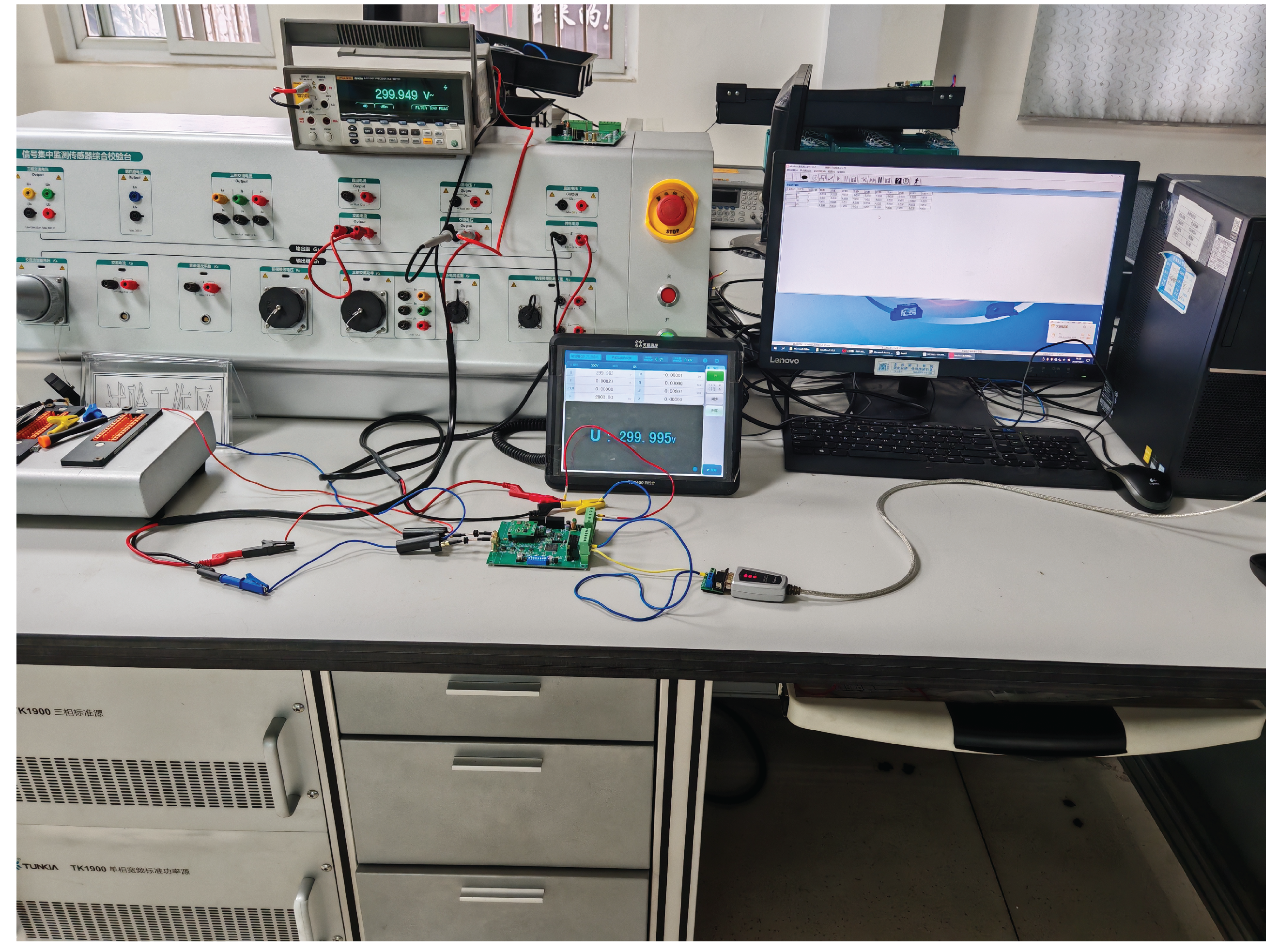
The method proposed in this paper aims to address the challenges of non-contact online voltage monitoring. Two prototype devices were fabricated and evaluated using signal cables with cross-sectional areas of 4.0 mm² and 2.0 mm², respectively. The conducted experiments included full-scale accuracy tests, nonlinearity error assessments, and evaluations of the effects of displacement variations on measurement accuracy. Furthermore, both prototypes underwent a continuous 48-hour powered operation test. During the experiments, the 4.0 mm² cable was used for full-scale calibration, and the relative position between the sensing probe and the printed circuit board was kept fixed to maintain a constant input capacitance.
Table 3.
Benchmark Test Conditions.
| (V) | Cross-sectional area of the measured signal cable | |
|---|---|---|
| 0-500 | 50 | 4.0mm² |
| 0-500 | 50 | 2.0mm² |
| 0-300 | 2000 | 4.0mm² |
| 0-300 | 2000 | 2.0mm² |
During the experiments, a standard single-phase wide band AC voltage source with an accuracy class of 0.05 was used to generate the test signal. A 6.5-digit high-precision bench top multimeter was employed to monitor the output voltage, serving as the reference for comparison with the prototype measurement results.
Figure 9.
Experimental Setup Diagram
6.2. Results
The experimental results demonstrate that the proposed method achieves excellent linearity, with variations in cable cross-sectional area and conductor position exerting negligible influence on the measurement accuracy. Nonlinearity errors are shown in the table below:
Table 4.
Measurement Data of Voltage Linearity at 2000 Hz, 30-300 V.
| Theoretical Value(V) | Measured Value(V) | Error(%) |
|---|---|---|
| 30 | 30.05 | 0.02 |
| 60 | 60.15 | 0.05 |
| 90 | 89.99 | 0.00 |
| 120 | 120.39 | 0.13 |
| 150 | 150.14 | 0.05 |
| 180 | 180.42 | 0.14 |
| 210 | 209.86 | 0.06 |
| 240 | 240.33 | 0.11 |
| 270 | 270.35 | 0.13 |
| 300 | 300.14 | 0.05 |
Table 5.
Measurement Data of Voltage Linearity at 50 Hz, 50-500 V.
| Theoretical Value(V) | Measured Value(V) | Error(%) |
|---|---|---|
| 50 | 49.88 | -0.25 |
| 100 | 100.24 | 0.24 |
| 150 | 149.81 | -0.13 |
| 200 | 199.70 | -0.15 |
| 250 | 250.24 | 0.10 |
| 300 | 300.54 | 0.18 |
| 350 | 350.50 | 0.14 |
| 400 | 400.59 | 0.15 |
| 450 | 450.74 | 0.16 |
| 500 | 500.49 | 0.10 |
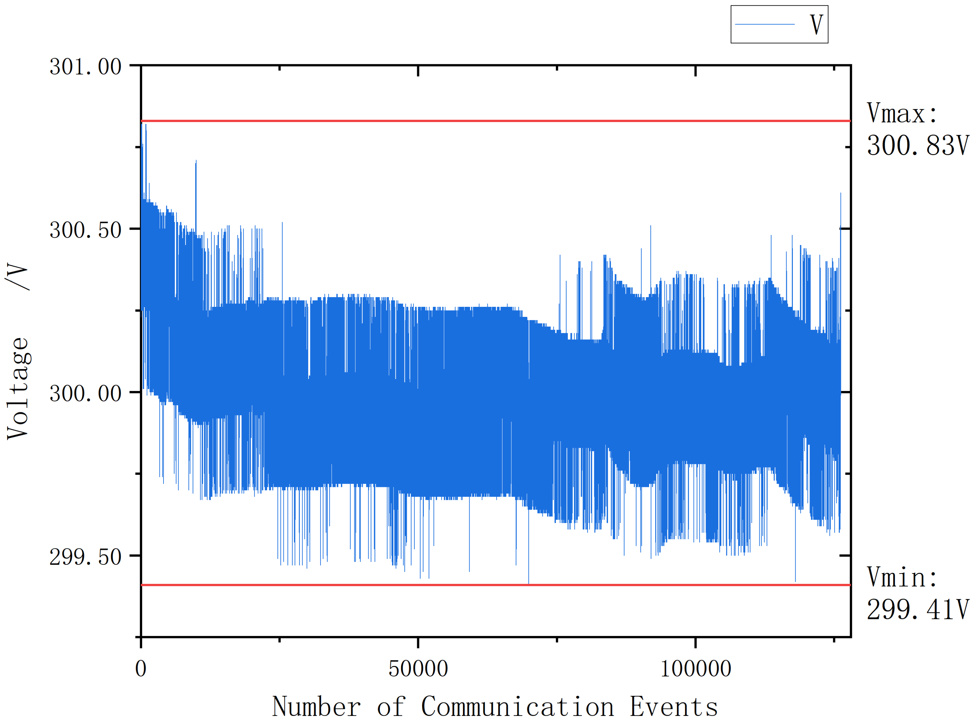
The non-linearity error for 50 Hz, 50-500 V voltage is also within 0.3To further evaluate its suitability for online monitoring applications, a continuous long-term power-on test was performed. Data acquisition was implemented via RS485 bus communication, with the host computer configured to sample data at 1-second intervals and a baud rate of 19,200 bps. The host computer functioned solely as a data logger and display terminal, without any additional data processing. The results of the long-term stability test are presented in Figure 10.
The test results show that a slight data drift occurs during the initial power-on phase, after which the measurements remain highly stable over extended operation. The initial drift is likely caused by thermal effects, which alter the distributed input capacitance on the printed circuit board as the circuit reaches thermal equilibrium.
7. Discussion
This paper presents an improved non-contact online voltage monitoring method designed to meet practical engineering requirements. A resistive–capacitive input structure is introduced to alleviate the constraints on printed circuit board layout. By employing a non-integer harmonic injection strategy, the issue of data fluctuations caused by relative phase drift in mixed-frequency signals is effectively mitigated, thereby improving measurement stability and accuracy. Experimental results demonstrate that the proposed method achieves class 0.5 accuracy for long-term online monitoring under room-temperature conditions, with negligible influence from cable replacement or minor variations in the feed-through position.
Experimental observations also indicate that the system is highly sensitive to distributed capacitance. Specifically, measurable deviations occur when the relative position between the sensing probe and the PCB changes, and data drift appears during the initial power-on period as the PCB gradually warms up. The probe position can be stabilized using dedicated mechanical fixtures, yet the observed thermal drift suggests that the method remains sensitive to temperature variations. While the current design satisfies room-temperature operational requirements, extending its performance to wide temperature ranges (e.g., outdoor environments) poses a significant challenge and represents an important focus for future research.
Author Contributions
Conceptualization, L.M.Y and X.J.P; methodology, L.M.Y; software, L.M.Y; validation, L.M.Y, N.W. and L.Z.J; formal analysis, L.M.Y; investigation, L.M.Y; resources, L.M.Y,N.W; data curation, L.M.Y; writing—original draft preparation, L.M.Y; writing—review and editing, X.J.P; visualization, L.M.Y; supervision, L.M.Y; project administration, L.M.Y; funding acquisition, X.J.P All authors have read and agreed to the published version of the manuscript.
Data Availability Statement
The original contributions presented in this study are included in the article. Further inquiries can be directed to the corresponding author(s).
Conflicts of Interest
The funders had no role in the design of the study; in the collection, analyses, or interpretation of data; in the writing of the manuscript; or in the decision to publish the results.
Abbreviations
The following abbreviations are used in this manuscript:
| PCB | Printed Circuit Board |
| MCU | Micro controller Unit |
| RMS | Root Mean Square |
References
- Ao, G.; Tang, J.; Li, D.; Zhang, W.; Yang, L.; Xu, Z. Research on Non-Invasive Voltage Measurement Method Based on Impedance Adaptation. Integrated Ferroelectrics 2024, 240, 517–533. [CrossRef]
- Balsamo, D.; Porcarelli, D.; Benini, L.; Davide, B. A new non-invasive voltage measurement method for wireless analysis of electrical parameters and power quality. 2013 IEEE SENSORS 2013, pp. 1–4. [CrossRef]
- Haberman, M.; Spinelli, E. A Noncontact Voltage Measurement System for Power-Line Voltage Waveforms. IEEE Transactions on Instrumentation and Measurement 2020, 69, 2790–2797. [CrossRef]
- Lawrence, D.; Donnal, J.; Leeb, S.; He, Y. Non-Contact Measurement of Line Voltage. IEEE Sensors Journal 2016, 16, 8990–8997. [CrossRef]
- Reza, M.; Rahman, H.A. Non-Invasive Voltage Measurement Technique for Low Voltage AC Lines. 2021 IEEE 4th International Conference on Electronics Technology (ICET) 2021, pp. 143–148. [CrossRef]
- Sun, S.; Ma, F.; Yang, Q.; Ni, H.; Bai, T.; Ke, K.; Qiu, Z. Research on Non-Contact Voltage Measurement Method Based on Near-End Electric Field Inversion. Energies 2023. [CrossRef]
- Suo, C.; He, M.; Zhou, G.; Shi, X.; Tan, X.; Zhang, W. Research on Non-Invasive Floating Ground Voltage Measurement and Calibration Method. Electronics 2023. [CrossRef]
- Walczak, K.; Sikorski, W. Non-Contact High Voltage Measurement in the Online Partial Discharge Monitoring System. Energies 2021. [CrossRef]
- Wang, T.; Liu, H. Research on Synchronous Measurement Methods Based on Non-Contact Sensing. 2024 IEEE 2nd International Conference on Power Science and Technology (ICPST) 2024, pp. 414–419. [CrossRef]
- xiangyu shen.; Xu, Y.; Zhuang, W.; Xie, N. A Non-Contact Voltage Measurement Technology for Three-Phase Cables. 2025 International Conference on Electrical Automation and Artificial Intelligence (ICEAAI) 2025, pp. 676–679. [CrossRef]
- Shenil, P.S.; George, B. Nonintrusive AC Voltage Measurement Unit Utilizing the Capacitive Coupling to the Power System Ground. IEEE Transactions on Instrumentation and Measurement 2021, 70, 1–8. [CrossRef]
- ShenilP., S.; Raveendranath, A.; George, B. Feasibility study of a non-contact AC voltage measurement system. 2015 IEEE International Instrumentation and Measurement Technology Conference (I2MTC) Proceedings 2015, pp. 399–404. [CrossRef]
- Haberman, M.; Spinelli, E. Noncontact AC Voltage Measurements: Error and Noise Analysis. IEEE Transactions on Instrumentation and Measurement 2018, 67, 1946–1953. [CrossRef]
- Delle Femine, A.; Gallo, D.; Landi, C.; Lo Schiavo, A.; Luiso, M. Low power contactless voltage sensor for low voltage power systems. Sensors 2019, 19, 3513.
- Zhang Wei, Li Xiaojian, L.J. Simulation Analysis of Non-contact Voltage Sensor Electrode. Mechanical & Electrical Engineering Technology 2021, 50, 41–45.
- Huang Rujin, Suo Chunguang, Z.W.Z.J.Z.X. Self-Calibration Method for Non-Contact Voltage Measurement Based on Impedance Transformation. Chinese Journal of Scientific Instrument 2023, 44, 137–145. [CrossRef]
- Šerlat, A.; Grzegrzółka, M.; Czuba, K. Two-tone RF signal phase drift measurement system. Measurement 2025, 243, 116183. [Google Scholar] [CrossRef]
Figure 1.
Equivalent Circuit Diagram of Capacitive Coupled Non-contact Voltage Measurement Probe.
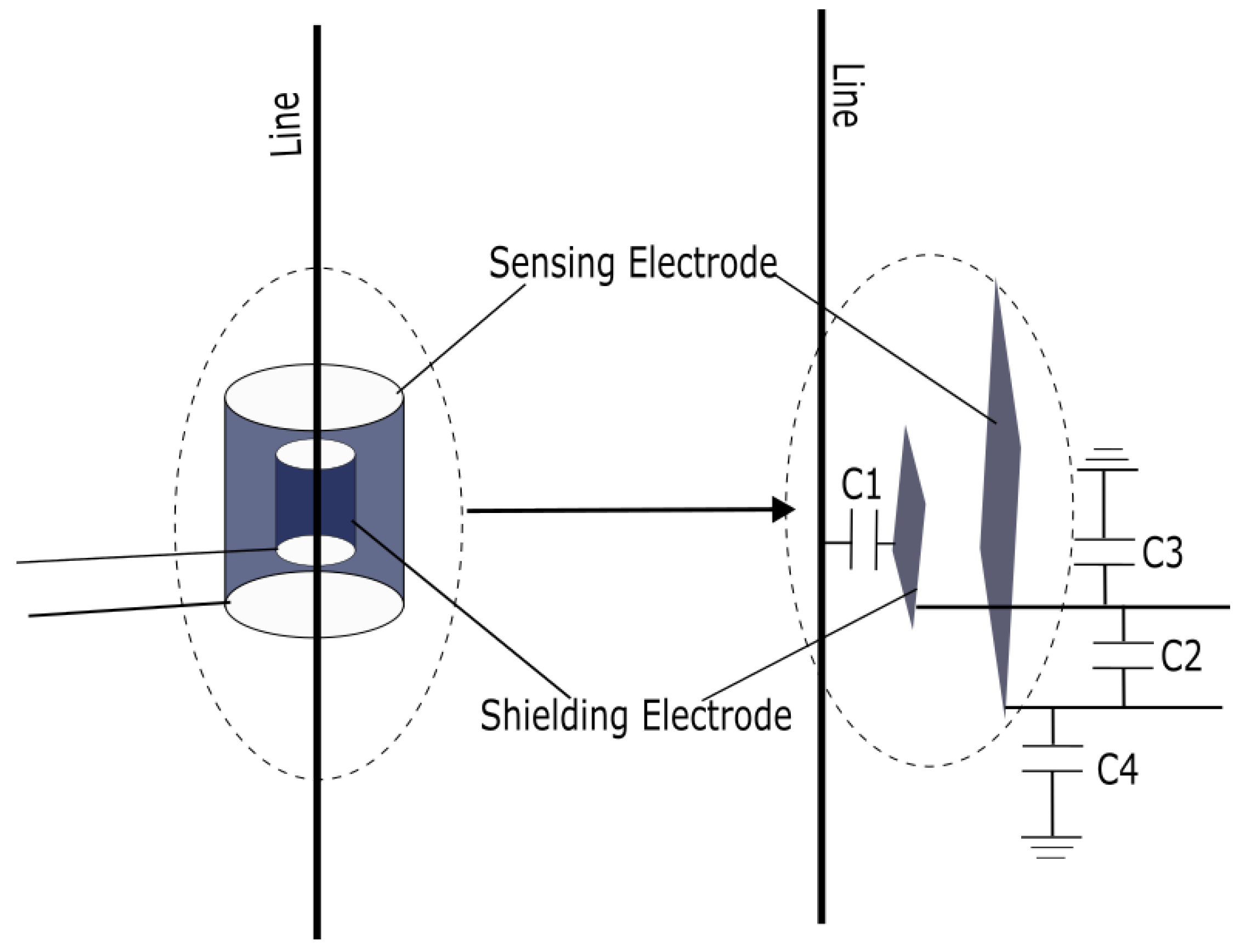
Figure 2.
Equivalent Circuit of Signal Injection-Based Capacitive Coupled Non-contact Voltage Measurement .
Figure 2.
Equivalent Circuit of Signal Injection-Based Capacitive Coupled Non-contact Voltage Measurement .
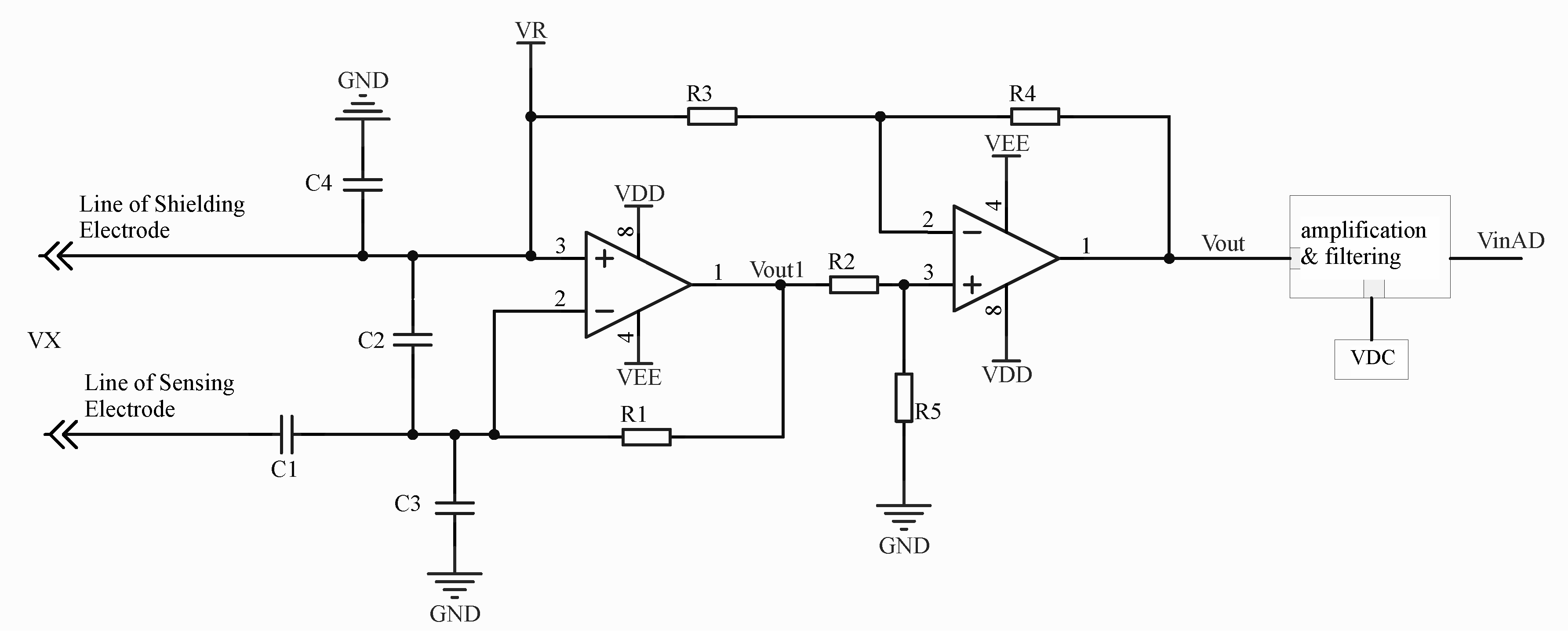
Figure 3.
Equivalent Schematic Diagram of Resistive-Capacitive Input.
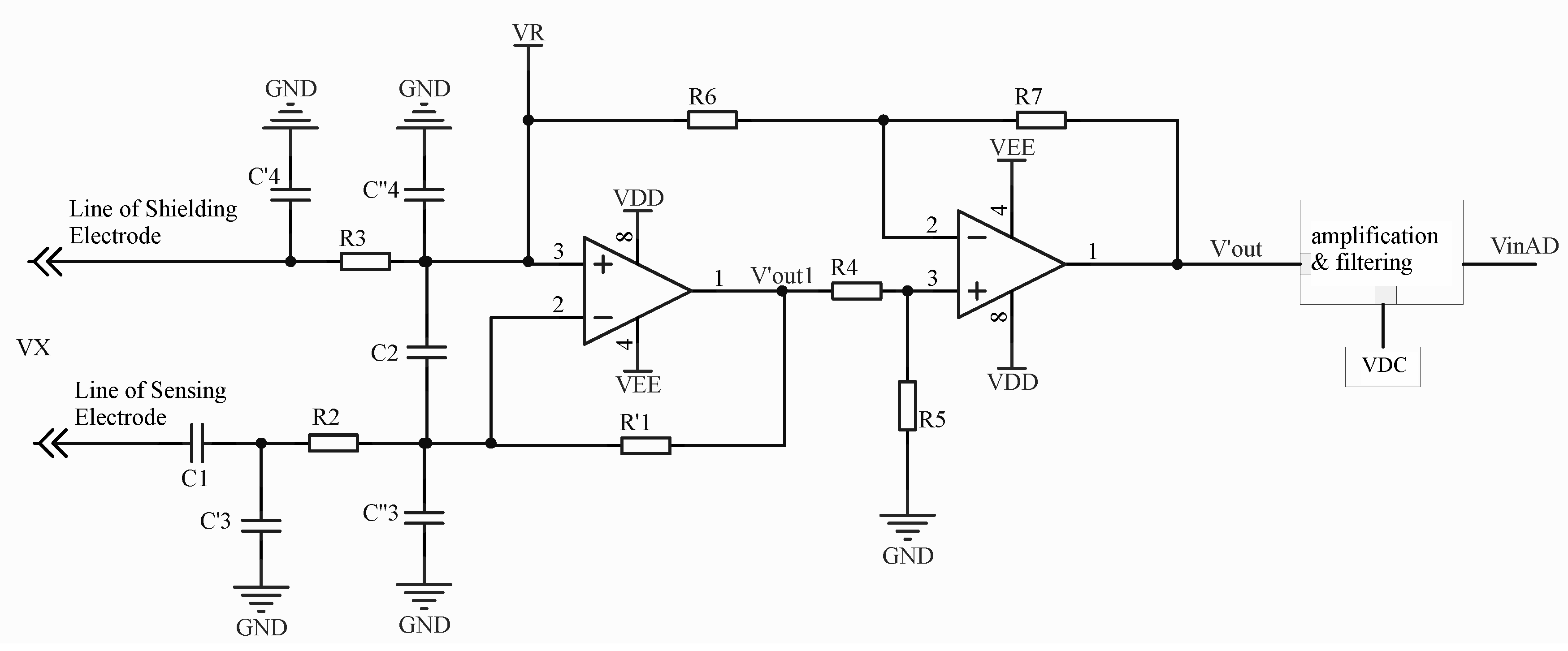
Figure 4.
Simplified Equivalent Circuit Diagram of Resistive-Capacitive Input
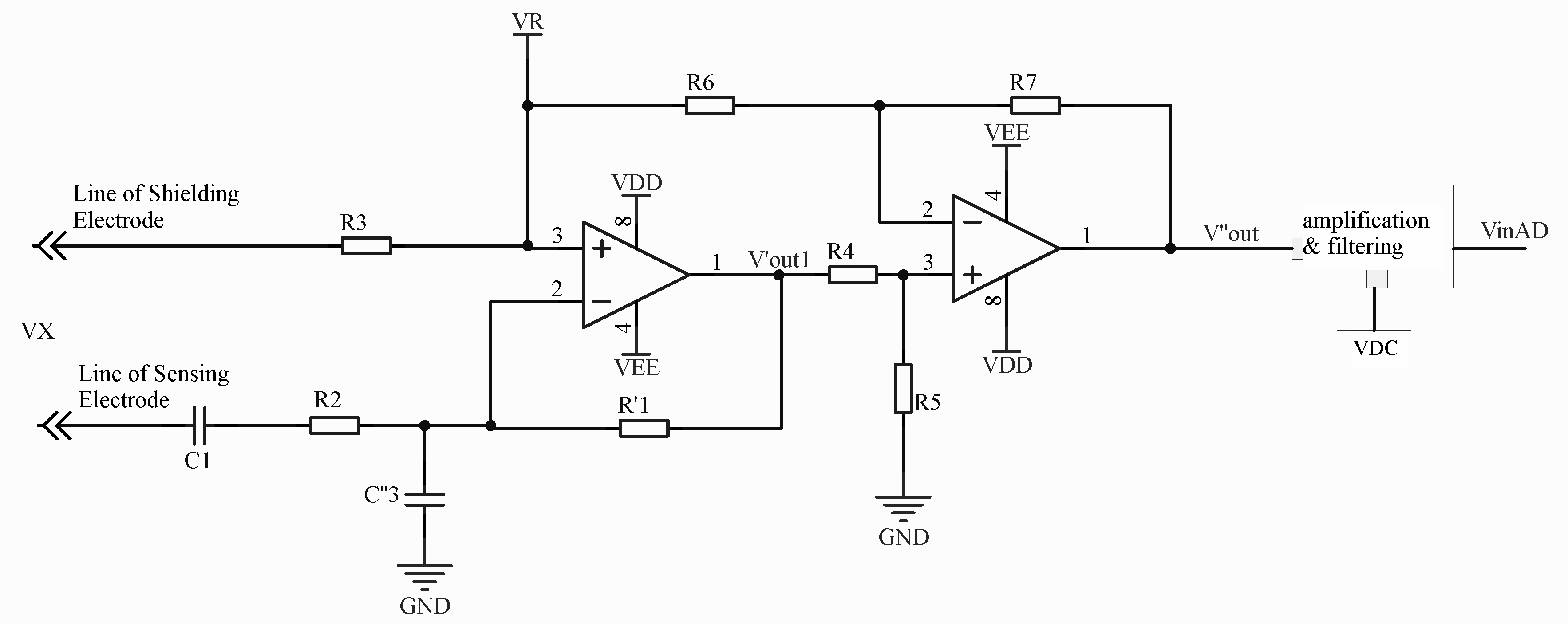
Figure 5.
Waveform of Input Signal at AD Port under Integer Harmonic Injection :(a) t=t1, (b)t=t2.
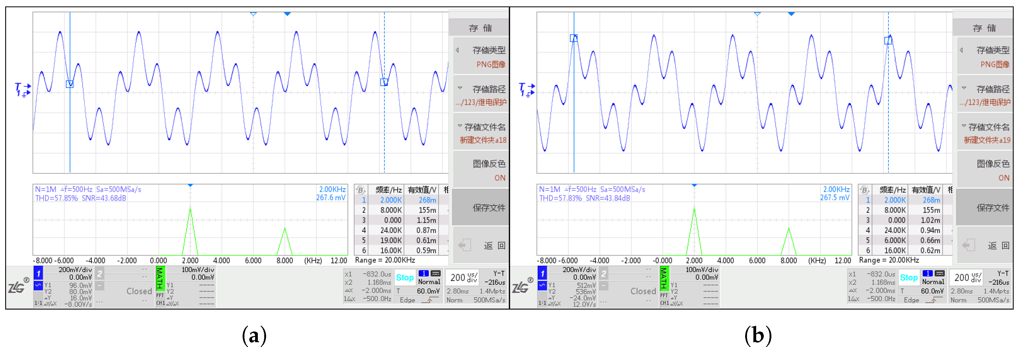
Figure 6.
Schematic Diagram of Test Results under Integer Harmonic Injection.
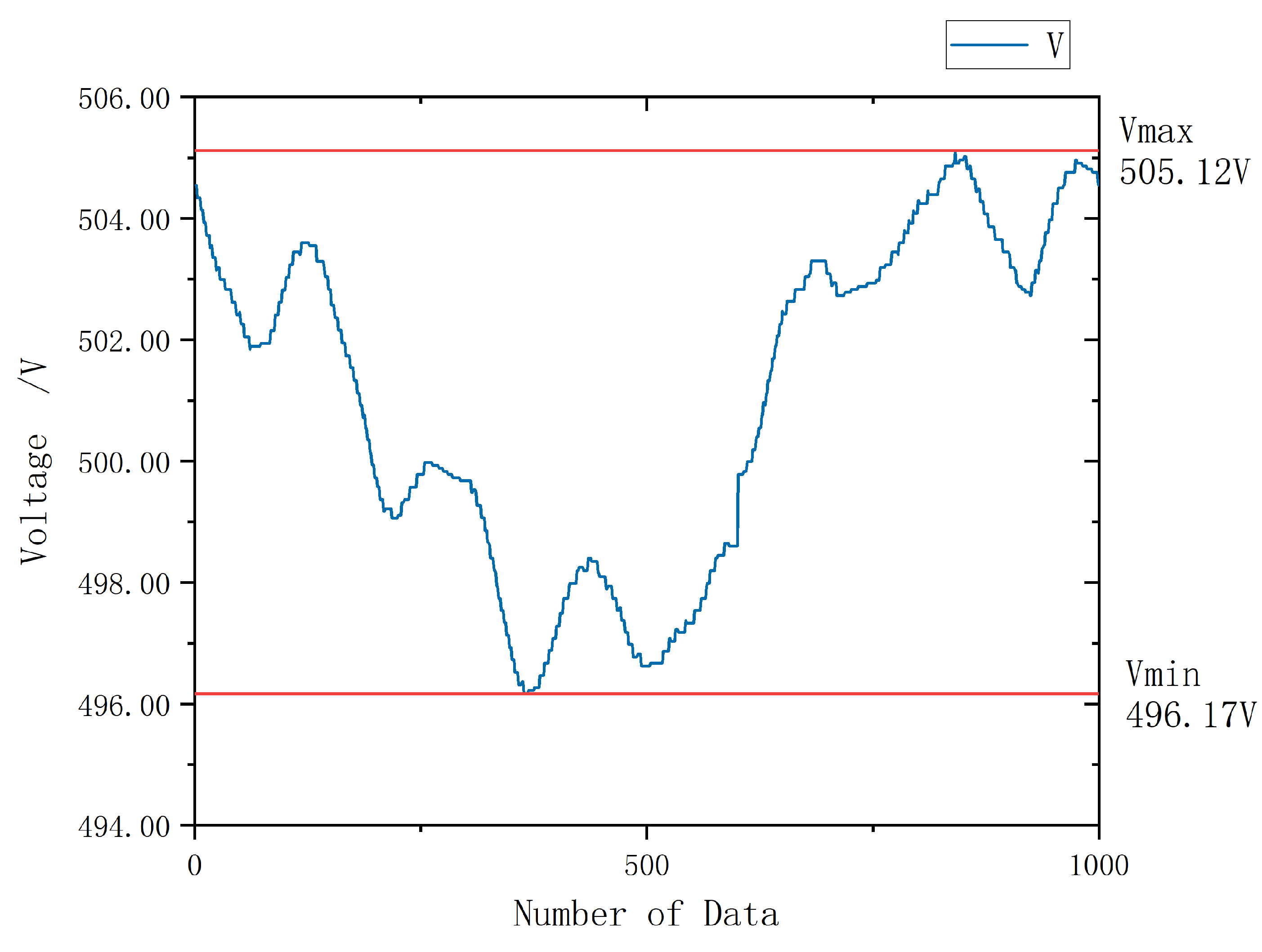
Figure 7.
Waveform of Input Signal at ADC Port under Non-Integer Harmonic Injection.
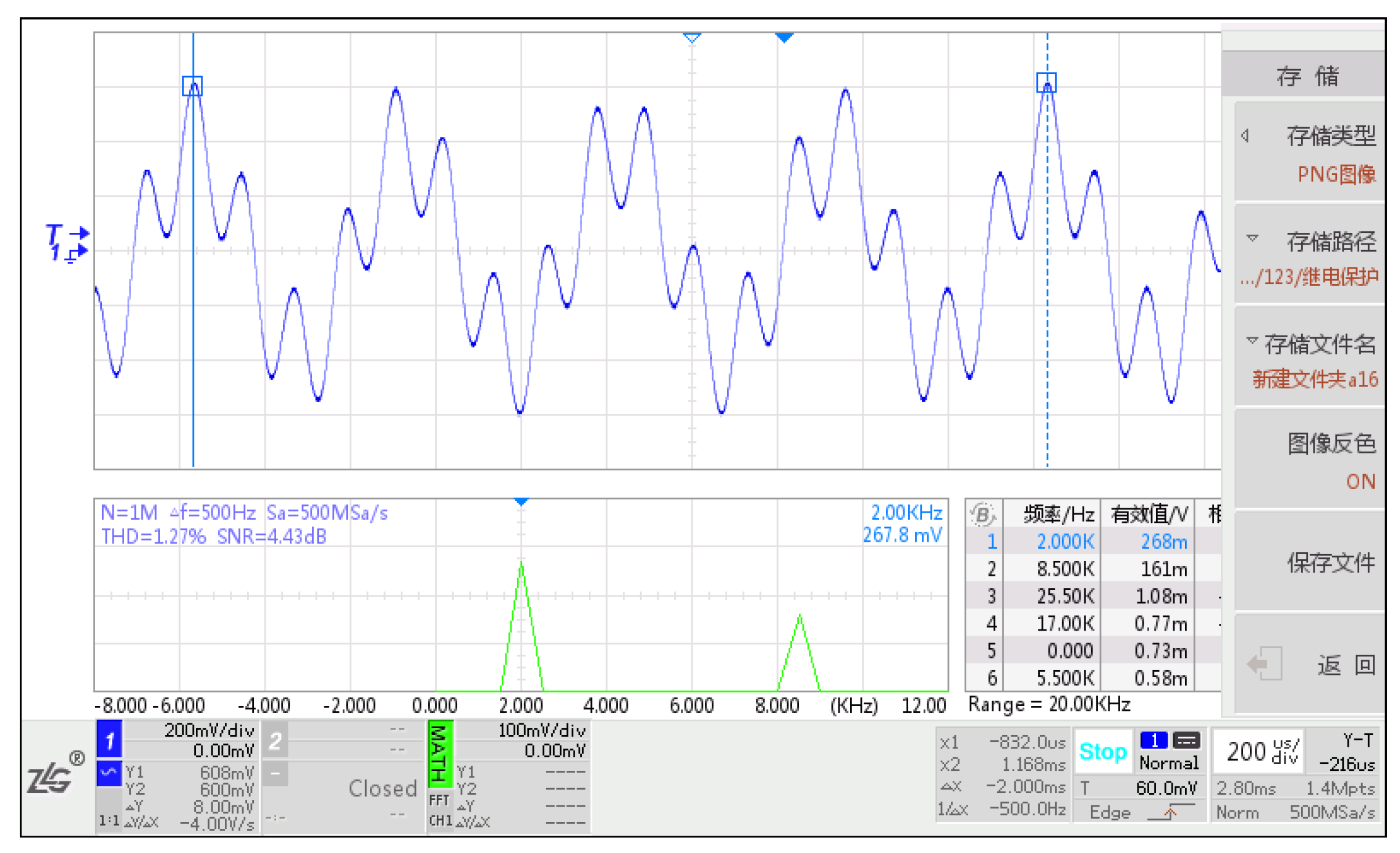
Figure 8.
Schematic Diagram of Test Results under Non-Integer Harmonic Injection
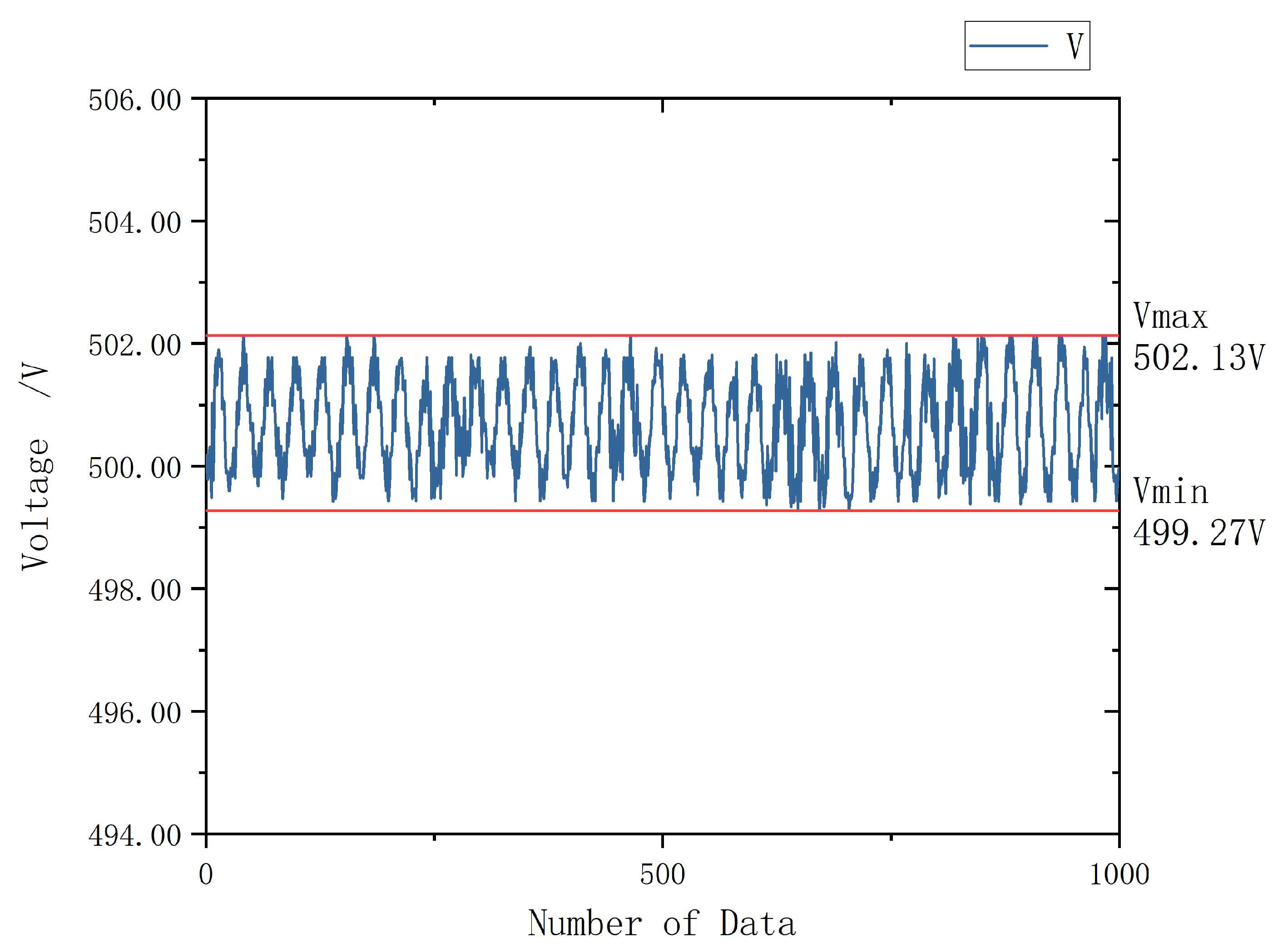
Figure 10.
Long-term Communication Data.
Disclaimer/Publisher’s Note: The statements, opinions and data contained in all publications are solely those of the individual author(s) and contributor(s) and not of MDPI and/or the editor(s). MDPI and/or the editor(s) disclaim responsibility for any injury to people or property resulting from any ideas, methods, instructions or products referred to in the content. |
© 2025 by the authors. Licensee MDPI, Basel, Switzerland. This article is an open access article distributed under the terms and conditions of the Creative Commons Attribution (CC BY) license (http://creativecommons.org/licenses/by/4.0/).
Copyright: This open access article is published under a Creative Commons CC BY 4.0 license, which permit the free download, distribution, and reuse, provided that the author and preprint are cited in any reuse.


