
Submitted:
15 December 2025
Posted:
17 December 2025
You are already at the latest version
Abstract
X-band copper resonating cavities are key components of future pulsed GHz normal conductive multi-TeV accelerators. Large electric gradients are required for new applications, but as the gradients increase, the components’ lifetime decreases due mainly to radiofrequency (RF) breakdown. Coating technology is under study in few laboratories to improve the performance and the lifetime of the RF structures. To this purpose, we studied the feasibility of fabrication of nanometer periodicity Cu/Mo metallic multilayers on three-dimensional (3-D) aluminum mandrels designed to replicate X-band copper resonating cavities. The nanometer period multilayers are proposed to mitigate surface degradation due to electric breakdown at high accelerating gradients, by stabilizing the inner cavity surfaces against dislocation evolution and roughening due to thermal-mechanical fatigue. High Power Impulse Magnetron Sputtering (HiPIMS) in a bias controlled dual closed field magnetron configuration is employed to deposit alternating Mo and Cu nanolayers onto the 3-D geometries. Due to the complexity of HiPIMS technology, the plasma pulse evolution is studied combining time resolved optical emission spectroscopy and pulse discharge electrical measurements. The influence of the process parameters and, particularly of the applied DC bias on film growth is studied with non-destructive microprobe α-particle Elastic Backscattering Spectrometry (µEBS) and by STEM electron microscopy. STEM and µEBS analyses confirm that Mo layers of thickness about 5-35 nm, can successfully be deposited repeatedly on thicker Cu layers (30-150 nm) preserving the individual properties with extremely limited interdiffusion and alloying of the layers deposited inside trenches with aspect ratios of 5:1 representative of X-band iris. The application of this technology for highly engineered nanostructured coatings in X-band cavities treatment, coupled to the replica process, might be envisaged for compact particles prototype accelerators, since it might improve the electrical breakdown lifetime at high accelerating fields, at least for the degradation processes caused by the high mobility of copper dislocations.
Keywords:
multilayer
; HiPIMS
; X-band cavity
; ionized sputtering
; ion assisted film growth
1. Introduction
New technologies to apply nanostructured coatings onto complex shapes are required in many research and industrial fields. In radio frequency (RF) superconductive resonating cavity accelerator technology, copper cavities are coated with pure niobium by physical vapor deposition since the late 1980s. Magnetron sputtering has been originally used for coating copper cavities whose typical size is of order of 10 cm. This technology is based on the deposition of pure niobium at ultra-high-vacuum (UHV) conditions by means of cylindrical magnetrons [1], UHV cathodic arc deposition [2] and ionized sputtering [3,4] for improving the quality of niobium and of other materials inside these copper cavities operated at cryogenic temperatures.
In parallel, the high gradient X-band technology based on microwave non-superconductive accelerating structures operating at 10-30 GHz in pulsed mode, with resonating cavities of much reduced size (of order of 1 cm) and much higher accelerating gradients has become a reality as the result of many years of intense R&D activity carried out at SLAC (US) and KEK (Japan) laboratories in the NLC (Next Linear Collider) and JLC (Japan Linear Collider) programs [5,6] and at CERN (Switzerland) in the context of the CLIC (Compact Linear Collider) development [7,8,9]. The microwave electromagnetic fields used in these accelerators are characterized by pulse duration typically in the range 15÷400 ns and typical 50÷200 Hz repetition frequency.
Due to the large investments involved, only few test facilities (SLAC [10], KEK [11], CERN [12,13], INFN (Italy) [14] and X-Lab (Australia) [15] are involved in the test and development of X-band technologies for next generation multi-TeV linear colliders. This restricts access for systematic testing, thereby potentially slowing technology validation. Therefore, new prototypes, such as multilayer reinforcement coating explored in this work, should be assessed both in terms of material performance and in relation to their integration within the existing test infrastructures.
The technological goal to decrease size and related costs of the next generation linear multi-TeV particle accelerators is driven by demanding requirements such as accelerating gradients higher than 100 MV m-1 [16] endurance of materials under intense pulsed GHz electromagnetic fields, tight dimensional tolerances (at micrometer level) and ultra-smooth surface quality. The high accelerating gradients require high electromagnetic fields and power flows, which pose serious issues with the materials. It turned out that electrical breakdown with associated vacuum arcs [17] is very harmful for the X-band components and, at the end, limit their operation at high gradients and determine the lifetime of the device. To characterize the performance of the X-band accelerating structures, the electrical breakdown rate at a given gradient (i.e., the probability of vacuum arcing) has become one of the most important parameters. The expected exploitation time of Linear Colliders would be of order of 1010 -1011 in terms of RF pulses number, consequently the acceptable electrical breakdown rates of accelerating structures have been defined e.g., in [18,19,20,21] and an intense investigation has been carried out and is still running to study the root cause of the degradation mechanisms.
In the production technology of X-band accelerating structures the reference material is polycrystalline oxygen-free electronic grade (OFE) copper. Copper alloys such as CuZr, CuCrZr which are a mixture of pure copper with properly chosen materials to reduce the RF breakdown have been investigated [22]. Dilute binary system Cu-X (X=Ag, Cd, Hg, Au, In, Mg) are being investigated in development programs in response to the stress induced RF load and to the observed surface damage during electrical conditioning, envisaging potential improvements in breakdown tolerance [23,24].
Refractory metals like Mo have been proposed as the iris material or as the whole structure material [25,26].
Different approaches have been used for complex shape cavities realization, including high-precision machining of copper and alloys, electroforming and, recently, additive manufacturing. The main challenges are related to the required surface finish and the system high precision matching to design and final assembly, which might need high vacuum brazing and could cause discontinuous interfaces as well as alignment inaccuracies.
Mechanically worked copper surfaces are indeed composed of grains of different crystallographic orientation and size, that depends on production method, material purity and on mechanical and/or thermal pre-treatments. Additive manufacturing (AM) technologies enable the fabrication of cavities with complex geometries, directly integrating ancillary systems such as cooling circuits; however, the resulting surfaces are typically rough and often affected by high porosity [27].
Both mechanical high precision machining and AM of bulk systems deliver parts composed by grain with different crystallographic scales and orientation (from tens of up to hundreds of µm) [28,29], which promote the dislocation motion and the formation of roughness induced by surface fatigue.
Dislocations are involved in multiple mechanisms causing deformation of crystalline materials under stress. If a dislocation source is located near the surface, the application of stress will lead to topological modification of the surface [22,30,31].
The pulsed RF operation results in surface pulsed heating characterized by rapid temperature rise of several tens of degrees with associated compressive stress of order of hundreds MPa followed by relaxation in the time between pulses. This causes surface break-up by cyclic thermal fatigue that has been investigated with detailed surface analysis at the micrometer scale [21,22,32].
It has been shown that, in general, the level of pulsed heating surface damage was less on harder materials which usually have smaller grains. This is supported by a model proposed in [30].
The evolution of dislocation patterns in strained Cu and in other fcc metals has been studied at sub-micrometer level in [33]. Here the dislocations within the boundaries have been shown to rearrange themselves to form arrays of parallel dislocations at a ten to hundreds nm pattern scale, when a threshold strain is reached in the fcc metals (50% for Cu). Such protrusions and related roughening with periodical line repetition structure at the ten nanometers pitch have been observed not only on pristine surface crystal faces after high power RF tests, but also in post-electrical breakdown molten spots in RF tested samples [see eg.: [34]-Figure 4]. The observation of mobile dislocations in soft copper exposed to high fields has also been reported at the 10th International Workshop on Mechanisms of Vacuum Arcs [35]. A model has been presented where the stochastic fluctuations of the mobile dislocations’ density in copper may be responsible for electrical breakdown once a critical transition characterized by a deterministic density increase due to effects of external fields occurs [36].
Imperfections like micro voids are also present at or beneath the poly-crystalline copper surface. These may produce dislocation nucleation under moderate tensile stresses (like those induced by high surface electrical field) with formation of stable protrusions [37].
As far as the component’s degradation at high gradients, various mechanisms have been proposed for the initiation of the electrical breakdown, but due to the high complexity, this topic is still not completely understood and deserves further study of the material transformation at the nm scale and further experiments at extreme operation conditions and modelling [38,39]. In this paper we assume that the initially super-smooth poly-crystalline pure copper surface undergoes microstructural and morphological transformations at the nm to µm scale because of the pulsed microwave excitation and that the dislocations processes may be involved in triggering vacuum arcing at elevated surface local electric fields [40].
The study of metallic multilayers with nanometer periodicity in the context of cavity accelerator technology is motivated by the need to enhance the strength of vacuum surface materials and to reduce the dependence on underlying polycrystalline copper transformations, which ultimately may lead to stochastic electrical breakdowns at high accelerating gradients.
A mitigation strategy to reduce electrical breakdown related to copper dislocations mobility should then consist in adopting a suitable surface treatment or a coating which is capable of resisting to the adverse effects of dislocation motion and to surface break-up by cyclic fatigue, by stabilizing the copper surface and preserving, as much as possible, the surface topography and conductivity (electrical and thermal).
In this respect, early studies [41,42,43,44,45,46] proved that tens nanometer-scale metallic multilayered thin films do offer a potential route, under certain conditions, to high strength coatings characterized by toughness, hardness, cyclic work hardenability, stress, and adhesion suitable to reduce the adverse deformation effects of cyclic fatigue and roughening. The basic mechanism responsible for the enhancement of the surface properties is the closely spaced interfaces acting as barriers to the motion of dislocations through the coating itself. This concept, originally proposed by Koehler [47] for multilayers with large shear modulus mismatch between layers, was further intensively studied by many authors and demonstrated by many experimental data on superlattices deposited by physical and chemical methods, such as, application-specific nanoscale metallic multilayers, as reviewed in [48] and references thereof.
For the specific application, the identification of the materials in the multilayer metallic stack relies principally on the preservation of conductivity and on the thermal stability of the structure. Copper should be chosen as one of the two alternating materials in the stack since it is the base material in X-band technology. The thickness of the copper layers must be greater than that of the second metal to maintain conductivity. Moreover, the thickness of the second metal should be kept to a minimum value on the nanometer scale, enough to preserve the integrity of the layer stack, since its electrical and thermal properties are generally inferior to those of copper. The second metal must therefore have the capability of preserving the nanometer multilayer structure at high temperature, preventing diffusion of copper and alloying, thus acting as an effective diffusion barrier for copper migration. These chemical and thermal stability conditions are satisfied in principle by refractory metals which do not form Cu compounds: in facts the equilibrium phase diagrams of (as an example) the Mo-Cu, W-Cu, Nb-Cu and Ta-Cu alloy systems show no measurable solid solubility.
Although these systems are immiscible at equilibrium conditions, in a non-equilibrium process such as physical vapor deposition or ion irradiation and at the nanometer scale, the limit to which these metals react and dissolve into Cu in metastable solid solutions is extended [49,50].
Copper may penetrate through a very thin metal layer by low energy (of order of about 100 eV) implantation during ion assisted growth, forming mixed interfaces in nanometer periodicity multilayers. For these reasons the design of a nanometer diffusion barrier to copper is challenging and must be experimentally tested.
Molybdenum is a refractory metal that does not react with copper, and it is also used and accepted in X-band technology. An early investigation reported no diffusion of Cu through a 50 nm Ta film up to about 600 °C [51]. Sputter deposited Mo films with nanometer thickness have technological interest in several fields, for example, as diffusion barrier for Cu in thin films transistor liquid crystal display production. Thin Mo films of about 40 nm thickness have proven to act as barrier to copper diffusion up to 600 °C for copper deposited with different techniques [52].
The DC electrical resistivity of sputter deposited Mo films of 40 to 100 nm thickness is reported to be in the range 14÷55 µΩcm, while Copper layers deposited by DC magnetron sputtering have resistivity in the range 2.7÷5.5 µΩcm [52,53,54].
Recent studies on depositions by High Power Impulse Magnetron Sputtering (HiPIMS) of thin Cu and Mo nano-layers show that film electrical resistivity is influenced by process parameters such as pressure, DC bias and pulse duration Cu layers deposited by HiPIMS are reported to have resistivity as low as 2 µΩcm, while that of about 700 nm Mo obtained by HiPIMS can reach about 10 µΩcm, depending on the specific parameters [55,56].
Cu-Mo multilayers with nanometer periodicity have been recently successfully prepared by DC magnetron sputtering in the context of thermal management materials [57] Stable Cu/Mo nano-multilayers were deposited by magnetron sputtering at the temperature of 750 °C in [58]. Here the thickness of Molybdenum was 3 nm, and the Mo/Cu thickness ratio was 1:1.
The in-plane electrical resistivity of Cu-Mo nano-multilayers has been measured and compared to models in [59,60] showing that the in-plane resistivity increases with the inverse multilayer period and depends on grain boundaries within the layers and by electron scattering from interfaces. For Cu-Mo multilayers resistivity well below 20 µΩcm should be expected for multilayers with a period higher than 20 nm.
In conclusion Cu and Mo appear a good initial choice for the multilayer stack, where individual Cu and Mo nano-layers are expected to preserve their properties with very limited inter-diffusion at high temperature and could make a multilayer capable of blocking the dislocations propagation through the coating due to the difference of shear stress.
Applying a single functional coating or a nanometer periodicity multilayer to the 3-dimensional inner surface of small-sized normal conducting X-band cavities has not been reported so far, although the coating process can be beneficial for the lifetime of the components. Recently Mo oxides coatings on Cu RF components have been proposed to improve the breakdown performances [61], and their feasibility has been investigated to reduce the dark current in high gradient applications [62].
The coating process is challenging since the internal size of these resonating cavities is of order of a centimeter and the iris apertures are typically of few mm [20,26]. Hence the coating process from inside, using custom-made cylindrical magnetron technologies, as in the case of the larger RF superconductive cavities, is not feasible. To overcome this problem few alternative production methods might be applied. On one side a multistep procedure based on copper addition, such as electroforming, could be used. Here as a first step a perfectly shaped mandrel made, for example, of a suitable Aluminum alloy (1xxx series), which is the exact negative shape of the multi-cell cavity, is manufactured by state of art diamond turning and super-polishing techniques. The functional coatings (nanostructured single or multi-layer) and a thicker strengthening copper overcoating are then directly applied onto the mandrel using Physical Vapor Deposition (PVD) methods and finally copper is added by electroforming (or another additive manufacturing method) onto the coated mandrel to make the massive body of the cavity. As the last production step, the mandrel is chemically dissolved using an alkaline solution [28]. Depositing a coating onto sacrificial or re-usable Aluminum mandrels followed by Cu or Ni electroforming is the basis of industrial production of radio-astronomical microwave devices [63] and of grazing incidence hard x-ray astronomical, single- and multilayer mirrors [64,65,66]. A second viable fabrication method relies on the fabrication of copper X-band accelerating cavities with a ‘split-open’ geometry, which are then vacuum-sealed Ultra High Vacuum tight, by welding with different methods [67].
In both cases, as will be discussed in the next section, it is necessary to deposit high quality nanolayers into a 3-D trench-like geometry i.e.: along vertical walls and onto bottom of the trench. This geometry poses challenges on film thickness and conformity coverage that require the control of directionality of the deposition flux particularly on the vertical surfaces. For this reason, bias ionized sputtering, i.e. a sputtering technique where the sputtered atoms are partially ionized and an electric field provides metal-ions directionality, has been chosen as the deposition method since it has been proven to be adequate to depositions inside trenches and trench filling with various aspect ratios [53,68].
With this technique the metal ions from the plasma are accelerated across the sheath at normal incidence, and their energy can be finely controlled by changing the sample DC bias. This is of vital importance in nanometer periodicity multilayer deposition to improve the layers and interfaces quality (i.e: low interface roughness and intermixing) as detailed in [69,70,71,72]. Moreover, the DC bias can be easily varied during the deposition process providing different ion bombardment energies at each layer and interface to adapt the intrinsic stress of the final stack to the specific application, once the total number of bilayers is defined.
High Power Impulse Magnetron Sputtering (HiPIMS) has been chosen in the present study as the nano-layer deposition method, since it represents one of the most used plasma methods of ionized magnetron sputtering deposition [73,74,75,76,77,78].
In HiPIMS, very high-power pulses are applied to the magnetron target with peak voltages up to 1 kV or more and power densities of order of kW cm-2 to produce ultra-dense plasmas with electron densities up to 4 orders of magnitude higher than those obtained with standard DC magnetron sputtering. Power in HiPIMS systems is applied in short pulses (typically 50–200 µs) with duty cycles of order of 1% and frequencies from 10 Hz to several kHz. Since the strength and degree of balance of the magnetic field is extremely important in HiPIMS deposition to direct more ion flux to the substrate in the direction normal to the target surface [75,78,79] the magnetic field in front of the magnetrons is strongly unbalanced.
In this work the experimental setup and analytical tools used for the HiPIMS feasibility preparation of Cu/Mo nanometer multilayer coatings on the mandrels are described.
The primary objective is to demonstrate the feasibility of atomically depositing pure and stable nanometric metallic Cu/Mo multilayers by a complex HiPIMS process on specific 3-D geometries, using controlled bombardment conditions of ad-atoms flux and energy during single layers growth. The plasma deposition process is studied through time-resolved plasma optical and electrical properties and correlated to the layer deposition. Ion and electron microscopies have been used, for the purposes of the present study, to determine films thickness profiles and interfaces quality, deferring further optimizations and characterizations to a second stage of development for the specific application.
2. Materials and Methods
For making relatively fast and not expensive tests, the deposition process has been developed for small mandrels with few cells as shown in Figure 1 (like those described in [20,26]).
Although the cavity shapes and the geometry of the mandrels are undergoing continuous refinement through numerical electromagnetic simulations aimed at maximizing the achievable accelerating gradients, the overall dimensions and shapes reported in Figure 1 are sufficiently representative of the problem.
In particular, the nanostructured coating must cover the entire surface of the mandrel (or of the open structure in the ‘split-open’ configuration) especially in the grooves along the vertical walls and the deep curved bottoms and iris. These regions correspond to the cavity areas where electrical breakdown damage is concentrated.
The 2. Two rectangular magnetrons (target size: 240 x 130 mm2, Teer Coatings Ltd) in the closed magnetic field configuration [80] are facing with opposed magnetic polarities at variable magnetron-sample distances in the range 110-270 mm. The sputtering targets (Cu-99.995%, Mo-99.95% were supplied by Testbourne Ltd. Two different power supplies are used for HiPIMS deposition (TRUMPF-Huettinger TruPlasma HIPULSE 4001 – 1 MW/pulse, frequency up to 1 kHz and SINEX 1.2 MW - Chemfilt R&D AB - 50 Hz). The pulse duration was in the range 50-75 µs. The two power supplies are operated one at the time using aluminum alloy shutters to stop the not desired fluxes from the other magnetron sources. The plasma ignition gas is Ar (N60 purity) at the pressure of 0.45 Pa. Once the electrical and geometrical deposition conditions are fixed, the thickness of the nano-layers was determined by the duration of the deposition (i.e.: the total number of pulses) calibrated with Rutherford Backscattering spectrometry. The data reported in this work regard deposition times of 456 s for Mo and 720 s for Cu, at a repetition rate of 50 Hz and 48 Hz respectively.
The sample is kept in continuous rotation inside the dense plasma regions (Figure 2). It is water cooled, and DC biased in the range -50 V to -100 V during the pulsed HiPIMS deposition. A custom-made filter provides stability of the applied bias with negligible overshoot during HiPIMS pulses and protects the DC bias power supply from high peak current pulses. The surface of the DC-biased sample holder exposed to plasma was about S0 = 496 ± 10 cm2. The remaining part of the sample holder was protected from plasma by means of a stainless-steel grounded shield kept at less than 1 mm from the biased parts.
The voltage and current of the magnetrons and of the sample holder as a function of time are recorded using high band-pass current (Tektronix TCP404XL) and voltage (Tektronix P6015A) probes on a 6 channels Mixed Signal Oscilloscope (Tektronix MSO series 5).
Average Optical Emission Spectroscopy (OES) is accomplished using a CCD spectrometer (Ocean Optics MAYA 2000 Pro) coupled to a UV silica-clad-silica optical fiber bundle (with transmission starting from 190 nm) accurately protected from the deposition flux. Time averaged optical bands of interest are studied with this setup. The interesting emission wavelengths are deduced from NIST database [81].
Time resolved OES has been used to study the time evolution of the charged particles during and after the HiPIMS pulses at different positions from magnetrons to sample. Photons emitted during and immediately after the plasma pulses, sampled at various positions by means of silica cladded-silica optical fiber bundles (Verity Instruments Inc), are fed into a monochromator (Spectral Products Mod. DK240, with 3 interchangeable gratings). The achieved spectral resolution was in the range 0.1÷0.2 nm. A photomultiplier (Hamamatsu R1104) is used to detect the in-band photons. The photomultiplier signals are recorded with a digitizer (CAEN DT5751 2-4 channels, 10bit, 1-2 Gs/s) in self-triggered mode, with time resolution of 1 ns.
This system acquires the single-photon and trigger signals of each HiPIMS pulse on two separate analog input channels. To establish the correct correlation between plasma ignition and optical emission, we synchronized the trigger with each HiPIMS magnetron current pulse (see Figure 2). The current pulse typically lags the applied voltage by a significant time, typically in the order of tens of microseconds, depending on pressure, target material, pulse duration, frequency, and it jitters approximately 1-2% of the delay time [82].
In the experimental configuration used in this work the sampled photons from electronic transitions of the chosen Cu(I), Cu(II), Cu(III), Mo(I), Mo(II), Mo(III) lines are of order of tens to some hundreds per HiPIMS pulse and their emission varies considerably as a function of the distance from the magnetron and of the time during each pulse. To reach meaningful photon statistics the acquisition of the optical signals is performed by collecting the single photon and trigger signals and their associated timestamp for many thousands consecutive HiPIMS pulses. The collected single-photon data are then analyzed off-line for each spectral line to obtain the in-band photons counts vs time curves with a typical binning time amplitude of 1 or 2 µs, comparable to jitter time.
Individual and multiple Mo and Cu nano-layers have been prepared in various HiPIMS experimental conditions and characterized to understand and optimize the deposition process. For the feasibility study the coatings have been deposited onto small silicon witness plates positioned onto a test fixture that simulated the mandrel geometry reproducing a 2 mm wide, 10 mm deep trench in continuous rotation.
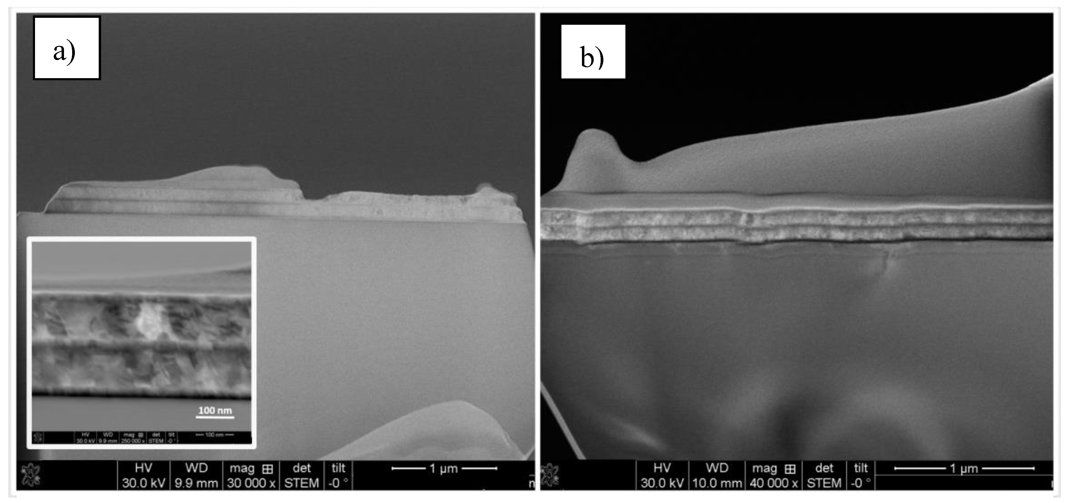
To study the layer growth along the vertical walls and on the bottom of trench and to study the penetration of the metal ion flux into the trench and any intermixing between Mo and Cu as a function of applied bias, several Si/Mo/Cu/Mo/Cu/Mo multiple layers have been prepared and characterized. These multiple layers have been analyzed with α-particle elastic backscattering spectrometry (µEBS) using the microprobe at the AN2000 accelerator of the Laboratori Nazionali di Legnaro with a beam spot size of about 20 x 20 µm2 at ΘEBS = 160°, Eα = 2000 keV, 15 keV FWHM energy resolution. µEBS has been chosen because it offers advantages over other widely used analytical techniques. First, µEBS allows to measure film thickness, purity and depth profile in one shot in a non-destructive way, with very high accuracy and excellent depth resolution. The non destructivity of the technique is mandatory to avoid artifacts such as interface mixing during depth profile (as, for example, in the AES and SIMS methods). As a second point, the µEBS analysis is performed on a small spot (20 x 20 µm2) at normal incidence. Other techniques, including standard EBS, with higher interaction size (0.5 to 1.0 mm) are not suited because the thickness of the nanolayers under investigation vary with the position on this scale so that the outcome would be only the average information of thickness and the interface quality between the individual layers cannot be assessed. To complement the Ion Beam Analysis, scanning transmission electron microscopy (STEM) was performed on selected samples. A FEI dual beam Quanta 3D FEG microscope has been used to mill, with the Gallium Focused Ion Beam (FIB), cross sectional lamellas of our coatings (perpendicular to sample surface including multilayer and substrate) of about 40 nanometer thickness and about 5 µm length, that have been analyzed with STEM up to a magnification of 400.000x both in Dark Field and Bright Field to optimize contrast level. Before milling a protective Pt layer was deposited on the top sample’s surface. STEM analyses at high magnification and contrast provided Cu crystallite size direct observation, besides giving a visual local picture of the multiple layers stack.
3. Results
3.1. HiPIMS Electrical and Optical Diagnostics
In Figure 3 representative voltage and current (VM(t), iM(t)) curves of the magnetrons and of the sample holder (VSH(t), iSH(t)) are shown for Mo and Cu for the case of -100 V applied bias. Since the plasma potential varies with time during the HiPIMS pulse, the negative bias on the sample holder was chosen to let the sample to be in the ionic bombardment condition for the entire pulse duration. This happened at bias values lower than approximately -25 V (±5 V) for both Mo and Cu. At higher values the sample is bombarded by electrons for a part of the pulse.
The current and voltage profiles of the magnetron discharges (Figure 3e), 3f)) are in line with the HiPIMS literature data. The HiPIMS pulse peak power is about 370 kW and 250 kW for Mo and Cu respectively. The lower power used for Cu was due to arching problems at magnetron voltages lower than -800 V: a stable operation, compatible with the foreseen deposition rates, was achieved by adjusting the pulse duration to 75 µs with a pulse voltage of -750 V.
The DC bias shows a slight overshoot of not more than +5 V during the period of the HiPIMS pulse (Figure 3a), 3b)). The original DC bias set-value is recovered in few ms. More interesting are the trends of the sample holder current curves for different sample to magnetron distances. As can be seen in Figure 3c), 3d), the sample current iSH(t) shows a peak in correspondence to the maximum value of iM(t). A further peak is detected with a variable delay after switching off the magnetron voltage pulse. The delayed peak shows up at magnetron power densities typical of HiPIMS, while it is not recorded for lower powers in the standard magnetron sputtering regime. The intensity of this second peak decreases with increasing distances from the magnetron indicating a decay of the plasma density towards the substrate [83]. Propagation speeds (slopes) calculated by least squares fit of the measured delay vs peak position were about 2.8 km s-1 for Mo and 3.2 km s-1 for Cu discharges. These numbers agree with literature data and models of ion speeds and solitary waves propagation away from target in HiPIMS discharges, as measured e.g. from electron density, that should be accompanied to metal ion transport to the substrate [84,85].
At the sample-to-magnetron distance of 110 mm the sample holder peak currents reached the maximum values of about 60 A for Mo and 100 A for Cu (Figure 3 c) d) respectively).
To understand the nature of the current profile iSH(t) on the sample holder and to investigate its relevance to the deposition process, time resolved OES has been used. In Figure 4 the time resolved optical emission from selected lines of Ar(I), Ar(II), Cu(I), Cu(II), Mo(I), Mo(II) are shown for the optical fiber position near to the sample holder. The monochromator slits and gratings have been changed for count-rate optimization at the specific spectral lines, therefore the OES intensities are not normalized.
Near the sample, i.e. in the plasma volume sampled by the optical fiber a few mm far from the outer mandrel surface, the Cu(II) and Mo(II) single charged metal ions optical transitions are clearly detected, and the signal peak positions agree with the iSH(t) measurements. Similar spectra, with considerably lower intensity, have been recorded for the double charged Mo(III) (not reported here) confirming that these single and double charged metal ions are transported from the magnetron source to the outer surface of the biased mandrel.
The contribution of the secondary electrons emitted from the sample surface bombarded by Cu and Mo ions and neutrals to iSH(t) is made of different contributions and can be estimated from models and experimental literature data [86,87,88,89,90,91,92]. At the low bias values used in this study (-50 V, -100 V) the “kinetic” electron emission coefficient by Cu and Mo ion impact is very low. The calculated “potential” electron emission of single charged Mo and Cu on Mo and Cu surfaces is zero. Emission of electrons from double charged ion impacts is expected, but the calculated emission coefficient will be much lower than 1. The Cu and Mo reflected particles from each target at the corresponding maximum self-sputtering energy were calculated with TRIM.SP Monte Carlo code [93]. These reflected particles fractions resulted in the range 3.5 10-2 to 4.5 10-2 and were characterized by a slightly over-cosine emission distribution and by low mean energy in the range 30 to 40 eV. Therefore, to a first approximation, we may neglect electron emission from sample holder and assume that the measured iSH(t) is due mostly to bombardment with single and double charged positive metal ions. The Argon ions bombardment contributes to iSH(t) mainly during the short-time ignition part of the HIPIMS pulse where the concentrations of metal ions is negligible, as can be seen in Figure 4 a), f). This is due to the Ar rarefaction effect [83,94,95,96]. In fact, the very high peak powers applied during HiPIMS, produces correspondingly high instantaneous sputtering rates such that sputtered atom pulses rarefy the Ar gas in the region in front of the target due to the large momentum and thermal transfer. During HiPIMS pulses, sputtering switches from being initially dominated by Ar ions at the beginning of each pulse to sputtering dominated by metal ions later in the pulse as observed in Figure 4 a), b), f), g).
The excited neutral metals (Cu(I), Mo(I)) spectra are also quite well measured (Figure 4d), 4i)) thus the material flux to the substrate is made of energetic metal ions and of neutrals.
3.2. Mo and Cu Nano-Layers Characterization
To determine the purity and thickness outside and along the vertical walls and at the bottom of the trench and to estimate the ion/neutral ratio of metal deposition and to study the penetration of the metal ions from plasma into the trench, the µEBS analysis of the nano-layers has been performed. The Cu and Mo metallic nano-layers resulted quite pure since the oxygen content was below the detection limit of the µEBS technique (of order of about 1 at %).
In Figure 5 some α-particles µEBS spectra of samples obtained with -50 V and -100 V bias are shown. The inset of Figure 5 a) shows the sample stack structure composed of 3 nano-layers of Mo and 2 layers of Cu. The α-particles backscattered from the surface of the topmost Mo layer are recorded by the Si detector at about 1700 keV. The individual Mo and Cu layers are singularly identifiable for some positions along the trench walls or on the bottom, as shown, as an example, in Figure 5b), 5f) and 5h). Partial signal overlapping takes place for other stack thicknesses, for which the individual layer thicknesses are extracted by numerical simulation using XRUMP [97] and SIMNRA 7 [98] codes. The measured individual layer thicknesses profiles deduced from the µEBS data at steps of 500 µm are reported in Figure 6. From the data in Figure 5a), 5e) the net metal layer deposition rates on the outer surface of the cylinder fully exposed to plasma are quantified for the two bias conditions: Cu(-50 V): 0.51 nm s-1, Mo(-50 V): 0.19 nm s-1 and Cu(-100 V): 0.27 nm s-1, Mo(-100 V): ≈0.1 nm s-1. The net deposition rate at -100 V bias is about a factor 2 lower than that at -50 V because of re-sputtering.
Along the vertical walls at about 1 mm from bottom (Figure 5b), 5f), at about 5 mm from bottom (Figure 5c), 5g)) and on the bottom of the trench (Figure 5d), 5h) the thicknesses of the nano-layers are significantly smaller than those in the outer surface. The Cu and Mo nano-layers thicknesses vary as a function of the position along the vertical walls as shown in Figure 6. On the bottom of the trench, which corresponds to the iris of the final replicated resonating cavity, the multilayer shows comparable thickness to those at the intermediate vertical positions. For the single-layer deposition duration of 456 s, the Mo single-layer thicknesses vary from about 35 to 6 nm from top to bottom along the vertical wall and are about 10 to 20 nm on the bottom of the trench. For the single-layer deposition duration of 720 s, the Cu layer thickness varies from 150 nm to about 35 nm from top to bottom along the wall and from 60 to 90 nm in the bottom. The Cu/Mo thickness ratios were in the range 4.3 to 6, and the period varied in the range 40 to 185 nm.
In the region towards the trench opening, the material profiles obtained at -100 V bias show a lower thickness with respect to those obtained at -50 V, reflecting the more energetic ionic bombardment that enhances the elemental self-sputtering with net material loss.
On the contrary, in the lower part and in the bottom of the trench, the thickness is slightly higher due to the partial re-deposition of the sputtered material. Moreover, for the same bias conditions, the thickness profiles of the same element in the various layers overlap within the experimental EBS errors, except for the Mo profile of the innermost of the three Mo layers which is deposited onto the silicon backing at -100 V bias (Figure 6d)) differently from the other two Mo layers that are deposited on copper. This may be partly explained by the sputtering yield amplification during the ion-assisted growth of nanometer Mo films under Mo self-irradiation onto substrates with different masses (in this case Si and Cu) [99,100] and it is in line with predictions based on our TRIDYN [101] calculations (not shown here). These data indicate that metal ions from the plasma are accelerated by the bias electric field and penetrate deep into the trench. On the other hand, since the Mo thickness profiles in the case of -50 V bias are overlapping for all the three Mo layers (Figure 6(b)), it can be concluded that, at this bias condition, atoms rearrangement under ion bombardment takes place only in 2D, i.e.: parallel to the growth surface, with negligible re-sputtering.
Detailed analyses of the α-µEBS spectral shapes confirm the limited intermixing of the Mo and Cu layers at nanometer scale in line with TRIDYN simulations. A complementary view of this finding is given by scanning electron transmission microscopy. As an example, in Figure 7, the STEM images of the cross-sectional lamellae of multiple layers in two different positions in the trench (Vbias= -50 V) are shown. The lamellae obtained by FIB milling have a thickness of about 40 nm. Figure 7(a) shows the deposited multilayer on the vertical wall at about 6.5 mm from bottom. In the inset (250.000x) the quality of the ~20 nm Mo coatings and of the Cu nano-crystalline layers can be clearly seen. The two copper layers are confined between the three Mo layers with Cu crystalline grains size lower than 100 nm (in the growth direction). Figure 7(b) (Vbias= -50 V) shows the STEM image of layers deposited on the bottom of the trench corresponding to the tip of the iris (in replicated geometry) of the cavity subjected to high damage during pulsed RF operation.
4. Discussion
Through the comparison of the total (ions + neutrals) elemental content, DµEBS, measured by α-µEBS on the outer surface of the sample (Figure 5a) and 5e)) to the ionic dose , calculated from the pulse ion currents iSH(t) (Figure 3c) and 3e)), we could make a crude estimate of the fraction of metal ions to neutrals impinging onto the sample.
The instantaneous ionic flux is readily deduced from the measured currents at the sample holder, by making some assumptions. As a first assumption, secondary electrons emission is neglected as discussed above. As a further assumption, triple-charged and higher state ions are not considered, therefore the sample holder current can be parametrized as
where is the ratio between the double to single ions currents. K is unknown but, to simplify the estimation, we assume that it is constant throughout the pulse duration and that 0 < K ≤ 1 , based on the detected presence of the double charged ions and of their recorded photon intensities. With these assumptions, using (1) and considering that double charged ions count twice to the electric deposited charge, is given by
where S0 is the sample holder area collecting the charges and C = 6.241 1018 (ions/Coulomb).
The total elemental content deposited by ions, (at/cm2), is obtained by integrating the instantaneous flux of charged particles , given in (2), over the metal deposition time interval in each pulse:
where t1 and t2 are extracted from the time-resolved OES data (see Figure 4). In this way the current is integrated only in the time interval where the metal ions show-up, disentangling their contribution from the electrical discharge current tails and from the Ar ions contributions; N is the total number of pulses per deposition; R is the re-sputtering coefficient. For Vbias= -50 V we assume R=0 (i.e: negligible re-sputtering) based on the discussion of thickness profiles of Figure 6b) above.
The ratio J(K)=Dion(K)/DµEBS, deduced from (3) and the µEBS data, represents the ratio of metal ions to the total flux at the sample. From the calculations regarding the Vbias= -50 V depositions, J(K) ranges from approximately 0.8 to 0.6 for Mo, while for Cu it ranges from 0.6 to 0.4 for 0 < K≤ 1 respectively. The ion-to-neutral Jion/Jn fraction for Mo results in the range from about 4 to 1.5, while for Cu it is between 1.5 to about 0.7 for 0 < K ≤ 1. These numerical ranges confirm the fact that low energy metal ions bombardment plays a fundamental role in the HiPIMS Mo and Cu film growth. These numerical ranges also provide the input flux ranges for the TRIDYN simulations of the film growth process, since both Cu and Mo nano-layers grow under simultaneous irradiation of very low energy (eV) neutrals and ions with two bombarding energies depending on the charge state and the DC-bias condition.
STEM and µEBS analyses confirm that Mo layers of thickness about 5-35 nm, can successfully be deposited repeatedly on thicker Cu layers (30-150 nm) preserving the individual properties with extremely limited interdiffusion and alloying.
This study shows that, using bias HiPIMS in strong unbalanced magnetron configuration, it is possible to coat with continuous high quality metallic nano-layers the surface of a mandrel characterized by mm-sized trenches with aspect ratio of 5:1 which replicates the negative shape of a cm-sized multi-cell X-band cavities. The measured thickness profiles show that the film thickness is not uniform along the walls and varies approximately by a factor 3 to 4 as a function of position and process parameters. This will not be critical for the foreseen application. At the bottom of the trench (i.e., where the electric breakdown phenomena in working replicated cavities are more concentrated) the nano-layer thicknesses are comparable to those at the middle vertical wall position.
The study also shows that Cu and Mo metal ions from HiPIMS plasma penetrate the trench and respond to the DC electrical field applied to the metallic sample. Low energy self-bombardment (below 100 eV) and high ion to neutral bombarding ratios during growth are necessary to guarantee the absence of interface mixing between the individual elements and to ensure that the interface roughness will not increase by the addition of further layers. This is very important from an application perspective, since the deposition process can be repeated many times to produce much thicker protecting multilayer coatings. The flexibility of the developed process allows for a variation of the DC bias in the range -30 to -100 V in the different stages of multilayer deposition, providing different ion bombardment energies (below 100 eV) at each layer and interface to adapt the intrinsic stress of the final stack to the final coating.
The application of this technology for highly engineered nanostructured coatings in X-band components treatment, might be envisaged for compact particles prototype accelerators, since it might improve the electrical breakdown lifetime at high accelerating fields, at least for the degradation processes caused by the high mobility of copper dislocations.
5. Conclusions
This study proves the deposition feasibility of Cu/Mo nanometer scale multilayers onto complex three-dimensional mandrels by bias-assisted HiPIMS. As demonstrated by µEBS and STEM measurements, the process achieves full coverage in structures with aspect-ratio of order of 5:1, while maintaining sharp interfaces and low interdiffusion of the materials, with nano-layers thicknesses ranging from about 5 to 35 nm and from 30 to 150 nm for Mo and Cu respectively.
Time resolved plasma diagnostics coupled to discharge electrical characterization and µEBS analyses confirm that the ion assisted film growth is characterized by a low energy (below 100 eV) high ion-to-neutral flux ratio (ranging from 0.7 to 4.5), which is essential for preserving layer quality and multilayer stack architecture.
The application of this technology for highly engineered nanostructured coatings in X-band cavities treatment, coupled to the replica process, might be envisaged for high endurance compact particles prototype accelerators, since it might improve the electrical breakdown lifetime at high accelerating fields, at least for the degradation processes caused by the high mobility of copper dislocations under pulsed RF operation. The process may be adopted also to the multilayer coatings on open 3-D structures prior to welding.
Future work will address the upscaling of the process to multi cell mandrels with further optimization of deposition parameters to allow for tens of bi-layers deposition and validation of coated RF components under representative RF loading and electric fields and correlation to the atomic structure of the films.
Author Contributions
Conceptualization, M.C. and V.R.; methodology, M.C. and V.R.; data curation, M.C. and V.R.; writing—original draft preparation, M.C. and V.R.; funding acquisition, V.R. The authors have read and agreed to the published version of the manuscript.
Data Availability Statement
The raw data supporting the conclusions of this article will be made available by the authors on motivated request.
Conflicts of Interest
The authors declare no conflicts of interest.
Abbreviations
The following abbreviations are used in this manuscript:
| HiPIMS | High Power Impulse Magnetron Sputtering |
| µEBS | Microprobe Elastic Back-Scattering Spectrometry |
| DC | Direct Current |
| OES | Optical Emission Spectroscopy |
| STEM | Scanning Transmission Electron Microscopy |
| FIB | Focusses Ion Beam |
| PVD | Physical Vapor Deposition |
| CCD AM |
Charge Coupled Device Additive Manufacturing |
References
- V. Arbet-Engels et al., “Superconducting niobium cavities, a case for the film technology”, Nucl Instrum Methods Phys Res A, vol. 463, no. 1–2, pp. 1–8, May 2001. [CrossRef]
- J. Langner et al., “Deposition of superconducting niobium films for RF cavities by means of UHV cathodic Arc”, Vacuum, vol. 80, no. 11–12, pp. 1288–1293, Sep. 2006. [CrossRef]
- A. Anders et al., “Deposition of Niobium and other superconducting materials with high power impulse magnetron sputtering: concept and first results”, in TUIOA06 Proceedings of SRF2011, Chicago, IL USA, 2011, pp. 302–308.
- M. Burton, A. Palczewski, A. M. Valente-Feliciano, C. E. Reece, and T. Jefferson, “Progress with Nb HiPIMS films on 1.3 GHz cu cavities”, 2019. [CrossRef]
- K. Takata, “Overview of NLC/JLC collaboration”, in Proceedings of LINAC2002, Gyeongju, Korea, 2002, pp. 254–258.
- P. Tenenbaum and C. Usa, “The JLC/NLC baseline design”, in Proceedings of the 2003 Particle Accelerator Conference, 2003, pp. 681–683.
- H. Braun et al., “CLIC 2008 parameters -CLIC Note 764”, 2008. Accessed: May 19, 2024. https://indico.cern.ch/event/38861/contributions/1821802/attachments/777055/1065598/par2007.pdf.
- P. N. Burrows, “The compact linear collider (clic) 2018 summary report”, 2018. [CrossRef]
- E. Sicking and R. Ström, “From precision physics to the energy frontier with the Compact Linear Collider”, Nat Phys, vol. 16, no. 4, pp. 386–392, Apr. 2020. [CrossRef]
- R. D. C. Ruth et al., “A Test Accelerator For The Next Linear Collider - SLAC-PUB-6293”, 1993.https://www.slac.stanford.edu/pubs/slacpubs/6250/slac-pub-6293.pdf.
- M. Yoshida et al., “The Status of Nextef; The X-band Test Facility in KEK”, in THP053 Proceedings of LINAC08, Victoria, BC, Canada, 2008, pp. 906–908. https://www.researchgate.net/publication/228968497.
- F. Tecker, “CLIC and CTF3”, J Phys Conf Ser, vol. 110, no. 11, p. 112005, May 2008. [CrossRef]
- A. Edwards, “X-Band LLRF Developments for High Power CLIC Test Stands and Waveguide Interferometry for Phase Stabilisation”, 2022. https://cds.cern.ch/record/2843363/files/CERN-THESIS-2022-245.pdf.
- C. Di Giulio et al., “TEX (TEst stand for X-band) at LNF”, The 2023 International Workshop on Future Linear Colliders, Aug. 2023, Accessed: Jul. 07, 2025. http://arxiv.org/abs/2308.03053.
- M. Volpi et al., “X-LAB: A very high-capacity X-band RF test stand facility at the University of Melbourne”, EPJ Web Conf, vol. 315, p. 02007, Dec. 2024. [CrossRef]
- N. Mounet Ed. (CERN, Geneva, Switzerland), European Strategy for Particle Physics - Accelerator R&D Roadmap. CERN Yellow Reports: Monographs (2022). [CrossRef]
- H. Timko et al., “Mechanism of surface modification in the plasma-surface interaction in electrical arcs”, Phys Rev B Condens Matter Mater Phys, vol. 81, no. 18, May 2010. [CrossRef]
- S. Dobert et al., “High Gradient Performance of NLC/GLC X-Band Accelerating Structures”, in Proceedings of the 2005 Particle Accelerator Conference, IEEE, 2006, pp. 372–374. [CrossRef]
- R. Corsini et al., “A high-gradient test of a 30 GHz copper accelerating structure, CLIC-NOTE-698”, 2006. https://www.researchgate.net/publication/242373966.
- V. Dolgashev, S. Tantawi, Y. Higashi, and B. Spataro, “Geometric dependence of radio-frequency breakdown in normal conducting accelerating structures”, Appl Phys Lett, vol. 97, no. 17, 2010. [CrossRef]
- S. T. Heikkinen, S. Calatroni, and H. Neupert, “Thermal Fatigue Issues in High Gradient Particle Accelerators - CLIC Note 648”, 2006. http://cds.cern.ch/record/921679/files/open-2006-004.pdf.
- L. Laurent et al., “Experimental study of rf pulsed heating”, Physical Review Special Topics - Accelerators and Beams, vol. 14, no. 4, Apr. 2011. [CrossRef]
- G. Wang, E. I. Simakov, and D. Perez, “Ab initio Cu alloy design for high-gradient accelerating structures”, Appl Phys Lett, vol. 120, no. 13, Mar. 2022. [CrossRef]
- M. Volpi et al., “High-Power, High Repetition Rate X-Band Power Source At X-Lab, The X-Band Laboratory For Accelerators And Beams At The University Of Melbourne”, in 16th International Particle Accelerator Conference, 2024.
- W. Wuensch, “Progress in understanding the high-gradient limitations of accelerating structures”, in THYMA02 APAC2007, https://accelconf.web.cern.ch/a07/PAPERS/THYMA02.PDF.
- B. Spataro et al., “Technological issues and high gradient test results on X-band molybdenum accelerating structures”, Nucl Instrum Methods Phys Res A, vol. 657, no. 1, pp. 114–121, Nov. 2011. [CrossRef]
- C. Sakib-Uz-Zaman and M. A. H. Khondoker, “A Review on Extrusion Additive Manufacturing of Pure Copper”, Metals (Basel), vol. 13, no. 5, p. 859, Apr. 2023. [CrossRef]
- B. Spataro et al., “High-power comparison among brazed, clamped and electroformed X-band cavities”, Nucl Instrum Methods Phys Res A, vol. 657, no. 1, pp. 88–93, Nov. 2011. [CrossRef]
- M. Mayerhofer et al., “Red and Green Laser Powder Bed Fusion of Pure Copper in Combination with Chemical Post-Processing for RF Cavity Fabrication”, Instruments, vol. 8, no. 3, p. 39, Jul. 2024. [CrossRef]
- S. V. Kuzikov and M. E. Plotkin, “Theory of thermal fatigue caused by RF pulsed heating”, Int J Infrared Millimeter Waves, vol. 29, no. 3, pp. 298–311, Mar. 2008. [CrossRef]
- M. Aicheler, “Influence of grain orientation on evolution of surface features in fatigued polycrystalline copper: A comparison of thermal and uniaxial mechanical fatigue results”, J Phys Conf Ser, vol. 240, p. 012051, Jul. 2010. [CrossRef]
- S. Heikkinen, S. Calatroni, H. Neupert, W. Wünsch, and G. Switzerland, “Status of the fatigue studies of the CLIC accelerating structures”, in MOPLS128 Proceedings of EPAC 2006, Edinburgh, Scotland, 2006, pp. 858–860.
- P. Landau, R. Z. Shneck, G. Makov, and A. Venkert, “Evolution of dislocation patterns in fcc metals”, in IOP Conference Series: Materials Science and Engineering, 2009. [CrossRef]
- G. Gatti et al., “X-band accelerator structures: On going R&D at the INFN”, Nucl Instrum Methods Phys Res A, vol. 829, pp. 206–212, Sep. 2016. [CrossRef]
- https://indico.cern.ch/event/1099613/, “MeVArc 2022 workshop.”.
- E. Z. Engelberg, A. B. Yashar, Y. Ashkenazy, M. Assaf, and I. Popov, “Theory of electric field breakdown nucleation due to mobile dislocations”, Physical Review Accelerators and Beams, vol. 22, no. 8, Aug. 2019. [CrossRef]
- A. S. Pohjonen, F. Djurabekova, K. Nordlund, A. Kuronen, and S. P. Fitzgerald, “Dislocation nucleation from near surface void under static tensile stress in Cu”, J Appl Phys, vol. 110, no. 2, Jul. 2011. [CrossRef]
- C. Z. Antoine, F. Peauger, and F. Le Pimpec, “Erratum to: Electromigration occurences and its effects on metallic surfaces submitted to high electromagnetic field: A novel approach to breakdown in accelerators”, Nucl Instrum Methods Phys Res A, vol. 670, pp. 79–94, Apr. 2012. [CrossRef]
- R. Shinohara, S. Bagchi, E. Simakov, S. V. Baryshev, and D. Perez, “Thermal and electric field driven rf breakdown precursor formation on metal surfaces”, Physical Review Accelerators and Beams, vol. 27, no. 5, May 2024. [CrossRef]
- A. Descoeudres, Y. Levinsen, S. Calatroni, M. Taborelli, and W. Wuensch, “Investigation of the dc vacuum breakdown mechanism”, Physical Review Special Topics - Accelerators and Beams, vol. 12, no. 9, p. 092001, Sep. 2009. [CrossRef]
- M. R. Stoudt, R. C. Cammarata, and R. E. Ricker, “Suppression of fatigue cracking with nanometer-scale multilayered coatings”, Scr Mater, vol. 43, no. 6, pp. 491–496, Aug. 2000. [CrossRef]
- M. R. Stoudt, R. E. Ricker, and R. C. Cammarata, “The influence of a multilayered metallic coating on fatigue crack nucleation”, Int J Fatigue, vol. 23, pp. 215–223, 2001. [CrossRef]
- A. Misra, H. Kung, D. Hammon, R. G. Hoagland, and M. Nastasi, “Damage Mechanisms in Nanolayered Metallic Composites”, International Journal of Damage Mechanics, vol. 12, no. 4, pp. 365–376, Oct. 2003. [CrossRef]
- A. Misra and H. Kung, “Deformation behavior of nanostructured metallic multilayers”, Adv Eng Mater, vol. 3, no. 4, pp. 217–222, 2001. [CrossRef]
- M. J. Buehler and A. Misra, “Mechanical behavior of nanocomposites”, MRS Bull, vol. 44, no. 1, pp. 19–24, Jan. 2019. [CrossRef]
- S. Zheng, Z. Yan, X. Kong, and R. Zhang, “Interface Modifications on Strength and Plasticity of Nanolayered Metallic Composites”, Jun. 11, 2022, Chinese Academy of Sciences. [CrossRef]
- J. S. Koehler, “Attempt to Design a Strong Solid”, Phys Rev B, vol. 2, no. 2, pp. 547–551, Jul. 1970. [CrossRef]
- A. Sáenz-Trevizo and A. M. Hodge, “Nanomaterials by design: A review of nanoscale metallic multilayers”, Nanotechnology, vol. 31, no. 29, May 2020. [CrossRef]
- A. G. Dirks and J. J. van den Broek, “Metastable solid solutions in vapor deposited Cu–Cr, Cu–Mo, and Cu–W thin films”, Journal of Vacuum Science & Technology A: Vacuum, Surfaces, and Films, vol. 3, no. 6, pp. 2618–2622, Nov. 1985. [CrossRef]
- Y. G. Chen and B. X. Liu, “Irradiation-induced alloying in immiscible Mo-Cu system through multilayer technique”, J Appl Phys, vol. 82, no. 8, pp. 3815–3820, Oct. 1997. [CrossRef]
- K. Holloway, P. M. Fryer, C. Cabral, J. M. E. Harper, P. J. Bailey, and K. H. Kelleher, “Tantalum as a diffusion barrier between copper and silicon: Failure mechanism and effect of nitrogen additions”, J Appl Phys, vol. 71, no. 11, pp. 5433–5444, 1992. [CrossRef]
- Y. W. Yen, Y. L. Kuo, J. Y. Chen, C. Lee, and C. Y. Lee, “Investigation of thermal stability of Mo thin-films as the buffer layer and various Cu metallization as interconnection materials for thin film transistor-liquid crystal display applications”, Thin Solid Films, vol. 515, no. 18, pp. 7209–7216, Jun. 2007. [CrossRef]
- J. Weichart, M. Elghazzali, S. Kadlec, and A.P. Ehiasarian, “PVD Processes in High Aspect Ratio Features by HIPIMS”, in Society of Vacuum Coaters, 52nd Annual Technical Conference Proceedings, 2009, pp. 201–206.
- G. K. Rane, S. Menzel, T. Gemming, and J. Eckert, “Microstructure, electrical resistivity and stresses in sputter deposited W and Mo films and the influence of the interface on bilayer properties”, Thin Solid Films, vol. 571, no. P1, pp. 1–8, Nov. 2014. [CrossRef]
- X. Liu, H. Bai, Y. Ren, J. Li, and X. Liu, “Influence of HiPIMS Pulse Widths on the Structure and Properties of Copper Films”, Materials, vol. 17, no. 10, p. 2342, May 2024. [CrossRef]
- Y.-L. Chen, Y.-C. Lin, and W.-Y. Wu, “Mo Contact via High-Power Impulse Magnetron Sputtering on Polyimide Substrate”, Coatings, vol. 12, no. 1, p. 96, Jan. 2022. [CrossRef]
- J. Yeom, G. Lorenzin, L. Ghisalberti, C. Cancellieri, and J. Janczak-Rusch, “The thermal stability and degradation mechanism of Cu/Mo nanomultilayers”, Sci Technol Adv Mater, vol. 25, no. 1, Dec. 2024. [CrossRef]
- Y. Cui, B. Derby, N. Li, N. A. Mara, and A. Misra, “Suppression of shear banding in high-strength Cu/Mo nanocomposites with hierarchical bicontinuous intertwined structures”, Mater Res Lett, vol. 6, no. 3, pp. 184–190, Mar. 2018. [CrossRef]
- T. Sasaki, T. Kaneko, M. Sakuda, and R. Yamamoto, “The electrical resistivity of Cu/Mo multilayered films”, Journal of Physics F: Metal Physics, vol. 18, no. 6, pp. L113–L117, Jun. 1988. [CrossRef]
- T. Kaneko et al., “Structures and electrical properties of Cu/Mo metallic multilayered films”, Journal of Physics F: Metal Physics, vol. 18, no. 9, pp. 2053–2060, Sep. 1988. [CrossRef]
- J. Scifo et al., “Molybdenum oxides coatings for high demanding accelerator components”, Instruments, vol. 3, no. 4, Dec. 2019. [CrossRef]
- P. Vidal García et al., “Effect of Molybdenum Coatings on the Accelerating Cavity Quality Factor”, Instruments, vol. 7, no. 4, Dec. 2023. [CrossRef]
- R. BANHAM et al., “Electroformed front-end at 100 GHz for radio-astronomical applications”, Microw J (Int Ed), 2005, https://www.microwavejournal.com/articles/664-electroformed-front-end-at-100-ghz-for-radio-astronomical-applications.
- M. P. Ulmer, R. Altkorn, M. E. Graham, A. Madan, and Y. S. Chu, “Production and performance of multilayer-coated conical x-ray mirrors”, Appl Opt, vol. 42, no. 34, p. 6945, Dec. 2003. [CrossRef]
- D. Spiga, G. Pareschi, G. Grisoni, and G. Valsecchi, “Hard X-ray multilayer coated astronomical mirrors by e-beam deposition”, in Advances in Mirror Technology for X-Ray, EUV Lithography, Laser, and Other Applications II, SPIE, Oct. 2004, p. 66. [CrossRef]
- R. Hudec, L. Pina, and A. V. Inneman, “Replicated grazing incidence x-ray optics”, in Proceedings Volume 4012, X-Ray Optics, Instruments, and Missions III, 2000, pp. 422–431. [CrossRef]
- V. A. Dolgashev, L. Faillace, M. Migliorati, and B. Spataro, “Investigations on the multiple-sector hard-copper X-band accelerating structures”, Nucl Instrum Methods Phys Res A, vol. 1063, Jun. 2024. [CrossRef]
- P. F. Cheng, S. M. Rossnagel, and D. N. Ruzic, “Directional deposition of Cu into semiconductor trench structures using ionized magnetron sputtering”, Journal of Vacuum Science & Technology B: Microelectronics and Nanometer Structures Processing, Measurement, and Phenomena, vol. 13, no. 2, pp. 203–208, Mar. 1995. [CrossRef]
- Z. Q. Ma and Y. Kido, “The atomic displacements on surface generated by low-energy projectile”, Thin Solid Films, vol. 359, no. 2, pp. 288–292, Jan. 2000. [CrossRef]
- X. W. Zhou and H. N. G. Wadley, “The low energy ion assisted control of interfacial structure: ion incident angle effects”, Surf Sci, vol. 487, no. 1–3, pp. 159–170, Jul. 2001. [CrossRef]
- X. W. Zhou and H. N. G. Wadley, “Low energy ion assisted control of interfacial structure: Ion fluence effects”, J Appl Phys, vol. 88, no. 10, pp. 5737–5743, Nov. 2000. [CrossRef]
- A. Patelli et al., “Ion bombardment effects on nucleation of sputtered Mo nano-crystals in Mo/B4C/Si multilayers”, Surf Coat Technol, vol. 201, no. 1–2, pp. 143–147, Sep. 2006. [CrossRef]
- V. Kouznetsov, K. Macák, J. M. Schneider, U. Helmersson, and I. Petrov, “A novel pulsed magnetron sputter technique utilizing very high target power densities”, Surf Coat Technol, vol. 122, no. 2–3, pp. 290–293, Dec. 1999. [CrossRef]
- J. T. Gudmundsson, N. Brenning, D. Lundin, and U. Helmersson, “High power impulse magnetron sputtering discharge”, Journal of Vacuum Science & Technology A: Vacuum, Surfaces, and Films, vol. 30, no. 3, May 2012. [CrossRef]
- A. Anders, “Tutorial: Reactive high power impulse magnetron sputtering (R-HiPIMS)”, J Appl Phys, vol. 121, no. 17, May 2017. [CrossRef]
- A. Hecimovic and A. Von Keudell, “Spokes in high power impulse magnetron sputtering plasmas”, Sep. 06, 2018, Institute of Physics Publishing. [CrossRef]
- Daniel Lundin, Tiberiu Minea, and Jon Tomas Gudmundsson, High Power Impulse Magnetron Sputtering. Elsevier, 2020. [CrossRef]
- C. Li, X. Tian, C. Gong, and J. Xu, “The improvement of high power impulse magnetron sputtering performance by an external unbalanced magnetic field”, Vacuum, vol. 133, pp. 98–104, Nov. 2016. [CrossRef]
- J. Bohlmark, M. Östbye, M. Lattemann, H. Ljungcrantz, T. Rosell, and U. Helmersson, “Guiding the deposition flux in an ionized magnetron discharge”, Thin Solid Films, vol. 515, no. 4, pp. 1928–1931, Dec. 2006. [CrossRef]
- K. Laing, J. Hampshire, D. Teer, and G. Chester, “The effect of ion current density on the adhesion and structure of coatings deposited by magnetron sputter ion plating”, Surf Coat Technol, vol. 112, no. 1–3, pp. 177–180, Feb. 1999. [CrossRef]
- https://www.nist.gov/pml/atomic-spectra-database, “NIST Atomic Spectra DataBase.”.
- G. Y. Yushkov and A. Anders, “Origin of the delayed current onset in high-power impulse magnetron sputtering”, in IEEE Transactions on Plasma Science, Nov. 2010, pp. 3028–3034. [CrossRef]
- D. Horwat and A. Anders, “Compression and strong rarefaction in high power impulse magnetron sputtering discharges”, J Appl Phys, vol. 108, no. 12, Dec. 2010. [CrossRef]
- K. B. Gylfason, J. Alami, U. Helmersson, and J. T. Gudmundsson, “Ion-acoustic solitary waves in a high power pulsed magnetron sputtering discharge”, J Phys D Appl Phys, vol. 38, no. 18, pp. 3417–3421, Sep. 2005. [CrossRef]
- J. Held and A. von Keudell, “Pattern Formation in High Power Impulse Magnetron Sputtering (HiPIMS) Plasmas”, Plasma Chemistry and Plasma Processing, vol. 40, no. 3, pp. 643–660, 2020. [CrossRef]
- H. Winter, F. Aumayr, and G. Lakits, “Recent advances in understanding particle-induced electron emission from metal surfaces”, Nucl Instrum Methods Phys Res B, vol. 58, no. 3–4, pp. 301–308, Jun. 1991. [CrossRef]
- H. Winter, H. Eder, F. Aumayr, J. Lörincik, and Z. Sroubek, “Slow-ion induced electron emission from clean metal surfaces: ‘Subthreshold kinetic emission’ and ‘potential excitation of plasmons,’” Nucl Instrum Methods Phys Res B, vol. 182, no. 1–4, pp. 15–22, Aug. 2001. [CrossRef]
- R. A. Baragiola, E. V. Alonso, J. Ferron, and A. Oliva-Florio, “Ion-induced electron emission from clean metals”, Surf Sci, vol. 90, no. 2, pp. 240–255, Dec. 1979. [CrossRef]
- A. Anders, J. Andersson, and A. Ehiasarian, “High power impulse magnetron sputtering: Current-voltage-time characteristics indicate the onset of sustained self-sputtering”, J Appl Phys, vol. 102, no. 11, 2007. [CrossRef]
- G. Holmén, B. Svensson, and A. Burén, “Ion induced electron emission from polycrystalline copper”, Nuclear Instruments and Methods in Physics Research, vol. 185, no. 1–3, pp. 523–532, Jun. 1981. [CrossRef]
- J. Ferron, E. V Alonso, R. A. Baragiola, and A. Oliva-Florio, “Electron emission from molybdenum under ion bombardment”, J Phys D Appl Phys, vol. 14, no. 9, pp. 1707–1720, Sep. 1981. [CrossRef]
- J. Lörinčík, Z. Šroubek, H. Eder, F. Aumayr, and H. Winter, “Kinetic electron emission from clean polycrystalline gold induced by impact of slow C+, N+, O+, Ne+, Xe+, and Au+ ions”, Phys. Rev. B, vol. 62, no. 23, pp. 16116–16125, Dec. 2000. [CrossRef]
- W. Eckstein, Computer Simulation of Ion-Solid Interactions, vol. 10. in Springer Series in Materials Science, vol. 10. Berlin, Heidelberg: Springer Berlin Heidelberg, 1991. [CrossRef]
- S. M. Rossnagel, “Gas density reduction effects in magnetrons”, Journal of Vacuum Science & Technology A: Vacuum, Surfaces, and Films, vol. 6, no. 1, pp. 19–24, Jan. 1988. [CrossRef]
- M. Palmucci, N. Britun, S. Konstantinidis, and R. Snyders, “Rarefaction windows in a high-power impulse magnetron sputtering plasma”, J Appl Phys, vol. 114, no. 11, Sep. 2013. [CrossRef]
- K. Macák, V. Kouznetsov, J. Schneider, U. Helmersson, and I. Petrov, “Ionized sputter deposition using an extremely high plasma density pulsed magnetron discharge”, Journal of Vacuum Science & Technology A: Vacuum, Surfaces, and Films, vol. 18, no. 4, pp. 1533–1537, Jul. 2000. [CrossRef]
- L. R. Doolittle, “Algorithms for the rapid simulation of Rutherford backscattering spectra”, Nucl Instrum Methods Phys Res B, vol. 9, no. 3, pp. 344–351, Jun. 1985. [CrossRef]
- M. Mayer, “SIMNRA, a simulation program for the analysis of NRA, RBS and ERDA”, AIP Conf Proc, vol. 475, no. 1, pp. 541–544, Jun. 1999. [CrossRef]
- S. Berg, A. M. Barklund, B. Gelin, C. Nender, and I. Katardjiev, “Atom assisted sputtering yield amplification”, Journal of Vacuum Science & Technology A, vol. 10, no. 4, pp. 1592–1596, Jul. 1992. [CrossRef]
- S. Berg and I. Katardjiev, “Resputtering effects during ion beam assisted deposition and the sputter yield amplification effect”, Surf Coat Technol, vol. 84, no. 1–3, pp. 353–362, Oct. 1996. [CrossRef]
- W. Möller and W. Eckstein, “Tridyn — A TRIM simulation code including dynamic composition changes”, Nucl Instrum Methods Phys Res B, vol. 2, no. 1–3, pp. 814–818, Mar. 1984. [CrossRef]
Figure 1.
Representative picture of a three-cell aluminum mandrel.
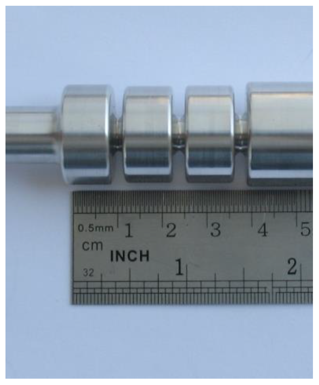
Figure 2.
Schematics of the bias closed magnetic field HiPIMS apparatus (side and top view) used for the deposition of the nano-layers, with related electrical and optical diagnostics.
Figure 2.
Schematics of the bias closed magnetic field HiPIMS apparatus (side and top view) used for the deposition of the nano-layers, with related electrical and optical diagnostics.
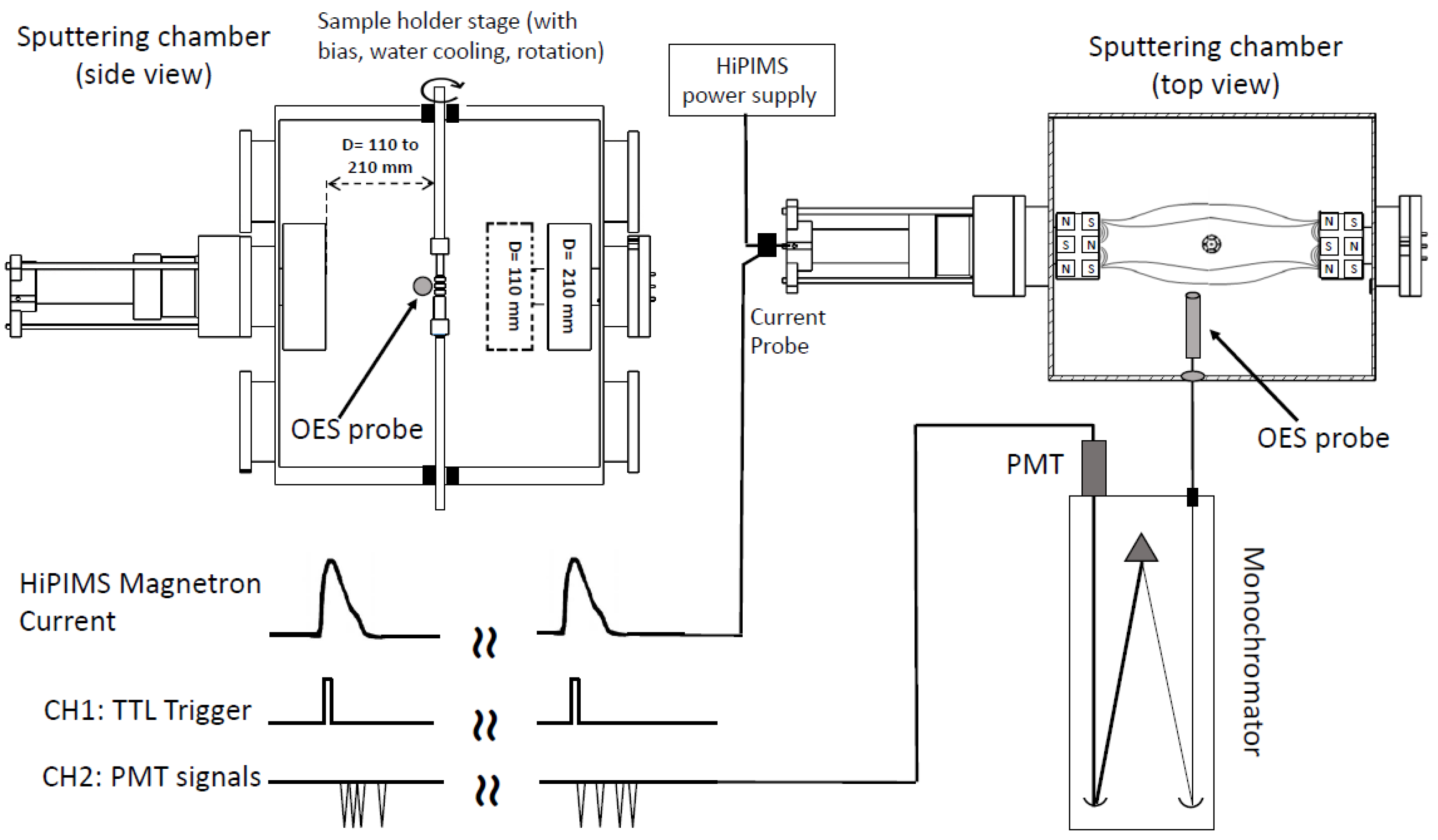
Figure 3.
Typical currents and voltages of the Mo (left) and Cu (right) magnetrons and of the sample holder at different sample-magnetron distances in the range 110-210 mm. PAr=0.45 Pa; repetition frequency: Cu: 48 Hz, Mo: 50 Hz. DC Bias: -100 V. a) b) sample holder bias voltage, c) d) sample holder current (|iSH(t)|), e) f) magnetron HiPIMS voltage and sputtering currents.
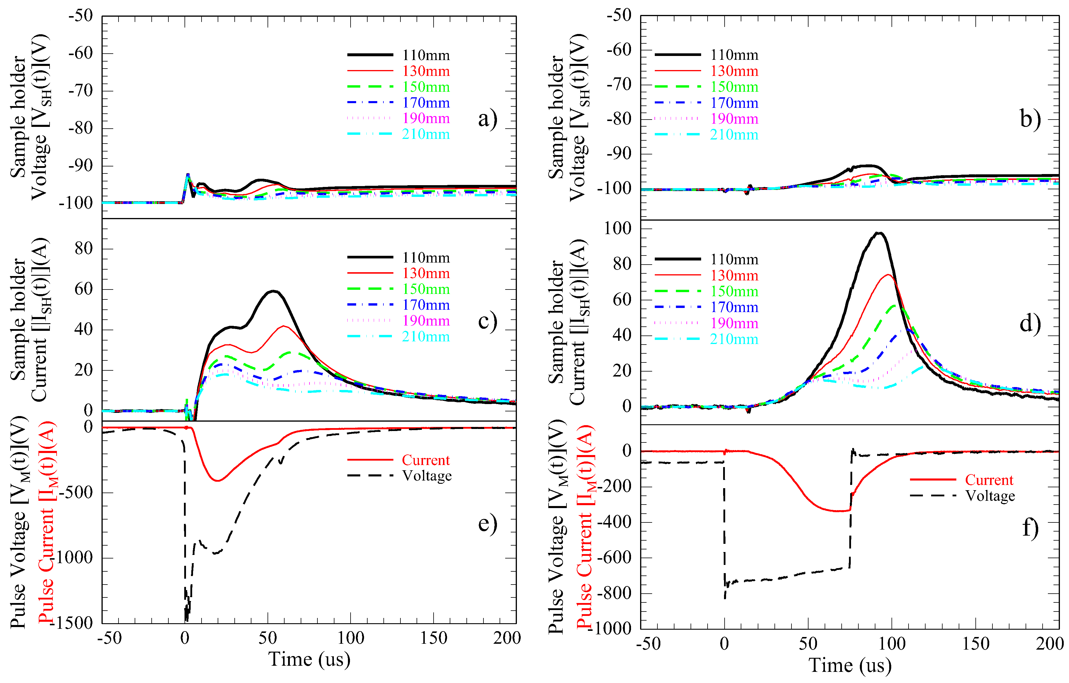
Figure 4.
Time resolved OES of argon, copper and molybdenum in the HiPIMS discharges, measured close to the sample holder. Target-sample distance: 110 mm. Binning time of processed data: 2 µs. a) Ar(II); b) Ar(I); c) Cu(II); d) Cu(I); e) iM(t), VM(t), |iSH(t)| for copper discharge. f) Ar(II); g) Ar(I); h) Mo(II); i) Mo(I); l) iM(t), VM(t), |iSH(t)| for molybdenum discharge.
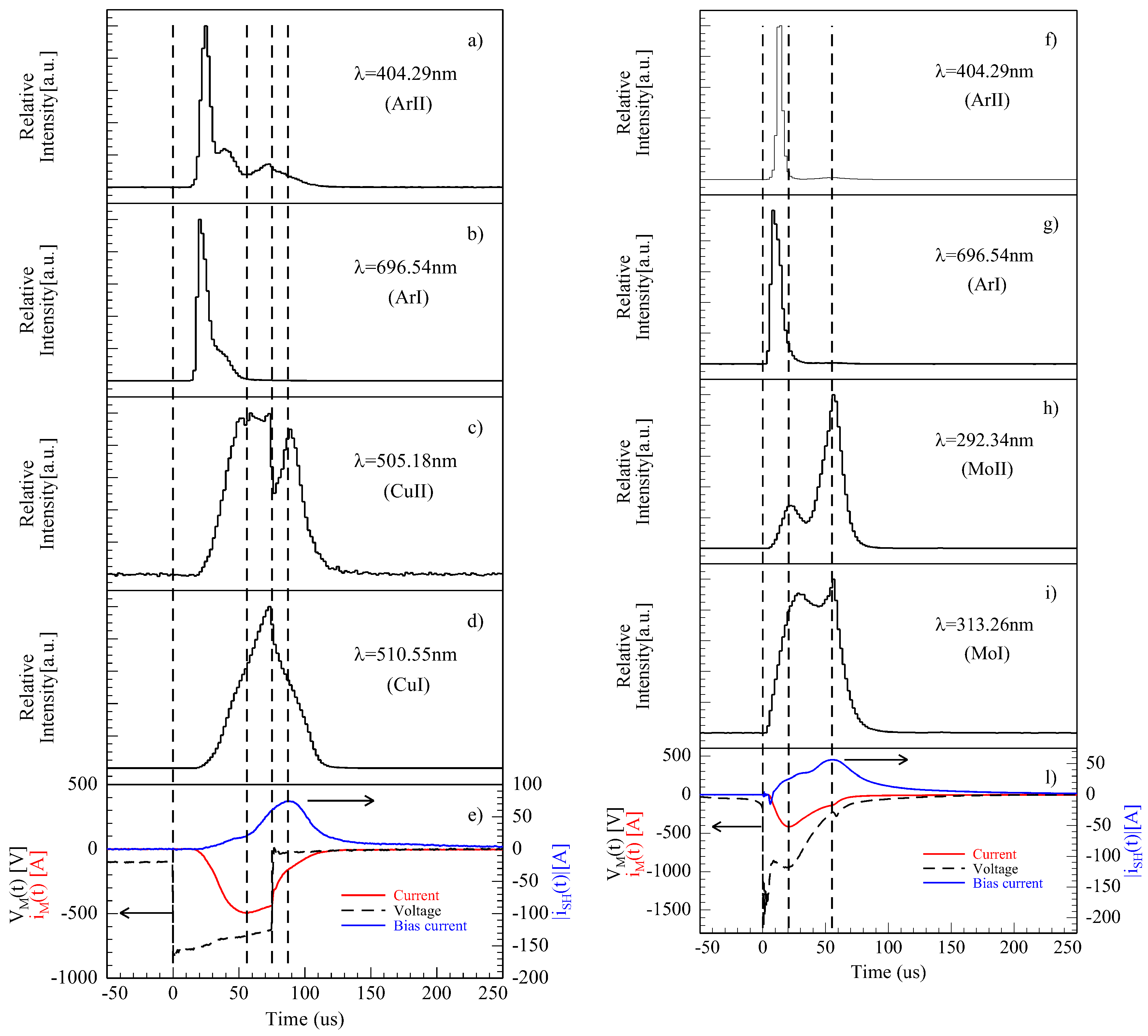
Figure 5.
Selected ΘEBS = 160°, Eα = 2000 keV α-particles µEBS spectra of multiple layers stack deposited at different bias (left: -50 V, right: -100 V) in different positions on the mandrel: a), e) outside the trench, fully exposed to plasma and deposition flux. b), f) 1 mm from bottom. c), g) 5 mm from bottom. d), h) at the bottom of the groove at center. Target to sample distance: 110 mm. 0.45 Pa Argon ignition pressure. The inset arrow indicates the position of EBS data taking in the trench.
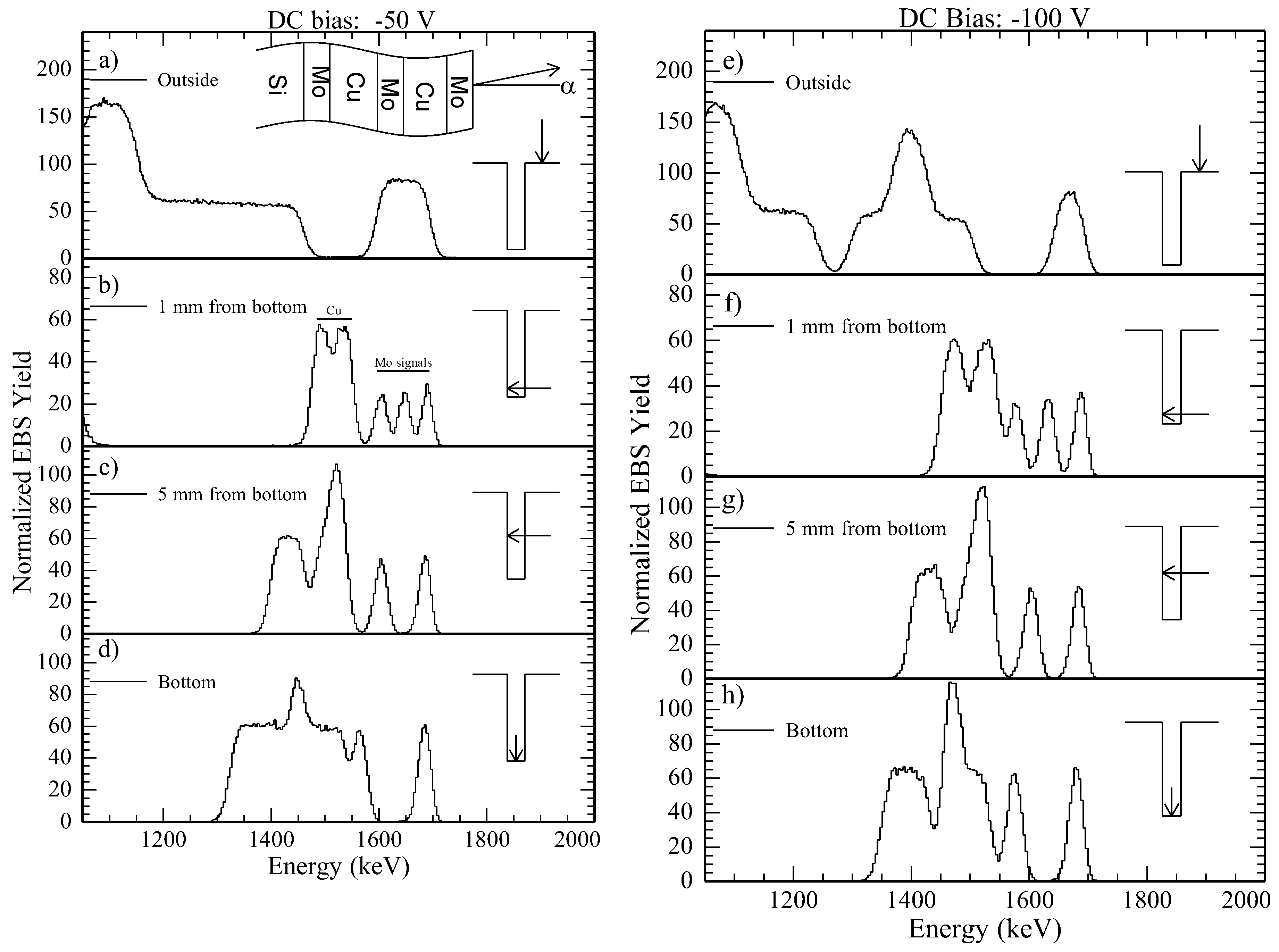
Figure 6.
Thickness of the 5 nano-layers of the Si/Mo/Cu/Mo/Cu/Mo stack as a function of the bias and position along the vertical wall b), d), f), h) and on the bottom of the trench a), c), e), g) as deduced from µEBS analysis. Open circles (red) refer to the first Mo layer deposited onto silicon. The position on the vertical wall is set to 0 at the bottom.
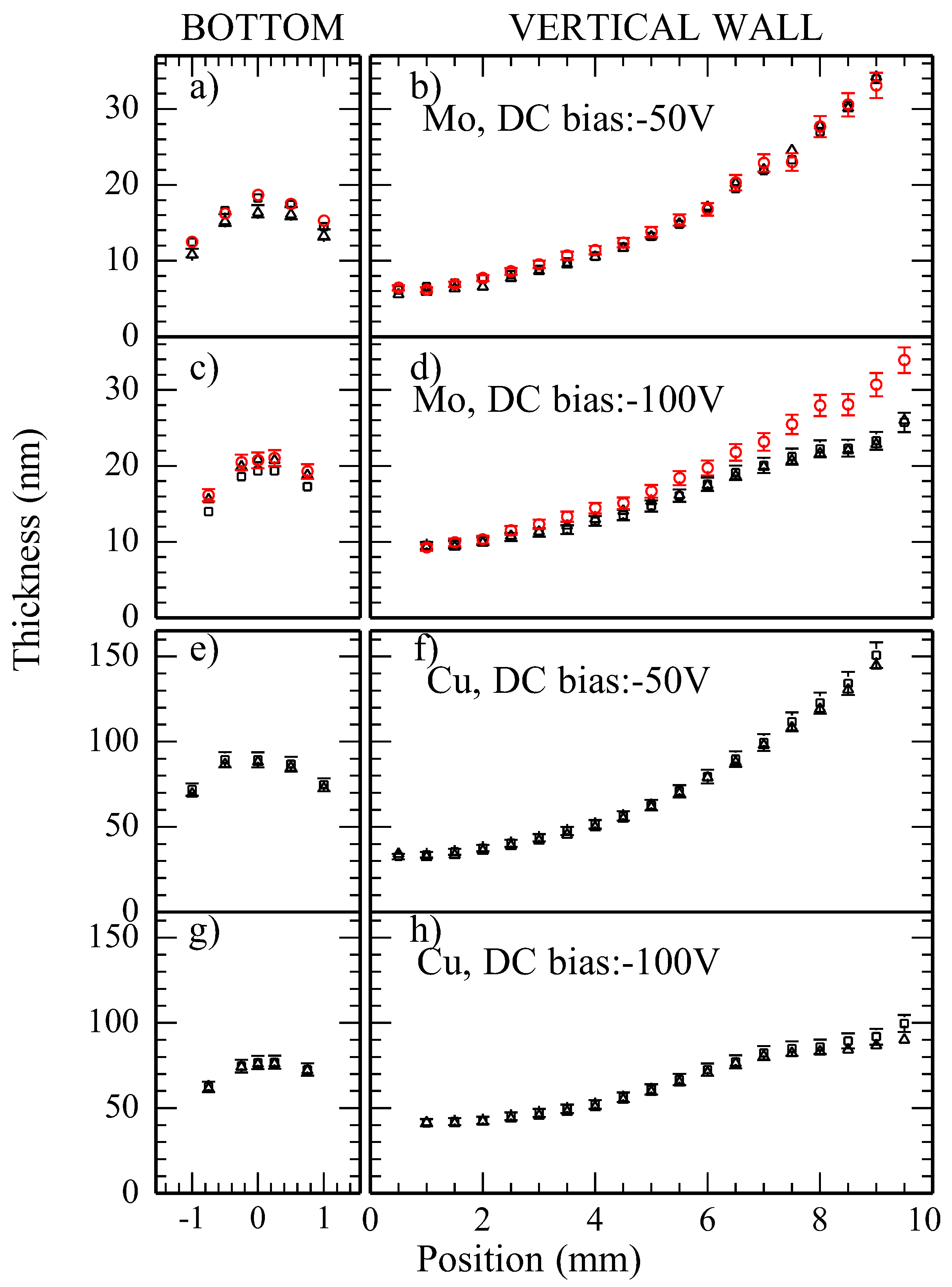
Figure 7.
STEM images of FIB milled cross sectional lamellae of two Si/Mo/Cu/Mo/Cu/Mo multilayers in different positions (DC bias = -50 V): a) 6.5 mm from bottom, b) at the bottom of the trench.
Figure 7.
STEM images of FIB milled cross sectional lamellae of two Si/Mo/Cu/Mo/Cu/Mo multilayers in different positions (DC bias = -50 V): a) 6.5 mm from bottom, b) at the bottom of the trench.
Disclaimer/Publisher’s Note: The statements, opinions and data contained in all publications are solely those of the individual author(s) and contributor(s) and not of MDPI and/or the editor(s). MDPI and/or the editor(s) disclaim responsibility for any injury to people or property resulting from any ideas, methods, instructions or products referred to in the content. |
© 2025 by the authors. Licensee MDPI, Basel, Switzerland. This article is an open access article distributed under the terms and conditions of the Creative Commons Attribution (CC BY) license (http://creativecommons.org/licenses/by/4.0/).
Copyright: This open access article is published under a Creative Commons CC BY 4.0 license, which permit the free download, distribution, and reuse, provided that the author and preprint are cited in any reuse.


