1. Introduction
Magnetron sputtering sources have been used in the semiconductor industry to form thin metal films during deposition [
1,
2]. Direct current (DC) magnetron sputtering is primarily used to deposit metal thin films [
3]. When ions accelerated by the potential distribution collide with the target metal with sufficient energy, they dislodge metal atoms. These sputtered atoms then travel to the substrate and are deposited. RF magnetron sputtering is mainly used to deposit thin films of insulating materials because it resolves the issue of charge accumulation on the dielectric, which can complicate the process [
4,
5,
6]. However, radiofrequency (RF) magnetron sputtering can also be used for metal deposition processes. It allows for easier discharge, extends the target’s lifespan, and enables ionized sputtered metal to reach the substrate, forming the coating material. In these processes, both neutral particles and ions are deposited onto the substrate, enhancing uniformity and adhesion, respectively [
7]. This characteristic of RF magnetron sputtering is distinct from that of general DC magnetron sputtering, and it is a feature of ionized metal physical vapor deposition (IMPVD). Previous studies have shown that the ionization rate of the sputtered metal in IMPVD can be up to 50% [
8], and voids may form if the ionization fraction is too low during metal deposition [
9]. Therefore, a gas discharge analysis is crucial to investigate the reactions contributing to the ionization of sputtered metal in the IMPVD process and to identify factors affecting deposition uniformity.
If the magnetron sputtering process continues, the metal target will eventually wear out and need to be replaced, which poses a problem in terms of cost and time. To address this, research has been conducted on rotating the magnet [
10] or combining both rotation and revolution [
11]. Additionally, the magnet can be configured in a cardioid shape and rotated to ensure that the target wears more evenly, thereby reducing the replacement cycle [
12]. Since the magnetic confinement of electrons and the increased plasma density due to ionization in the region contribute to the erosion of targets, it is essential to conduct research using particle-in-cell (PIC) simulations that can effectively explain the gyromotion and finite Larmor radius effects in magnetron sputtering devices, which are partially magnetized systems. In a previous study, the ion energy-angle distribution (IEAD) [
13] and the IEAD analysis of negative ions [
14], based on gas pressure changes in DC magnetron sputtering devices, were investigated. Additionally, studies were conducted to compare the IEAD and yield for eroded targets and flat targets [
15], and to investigate the effects of heating profiles, electron drift motion [
16], and rotating structures [
17].
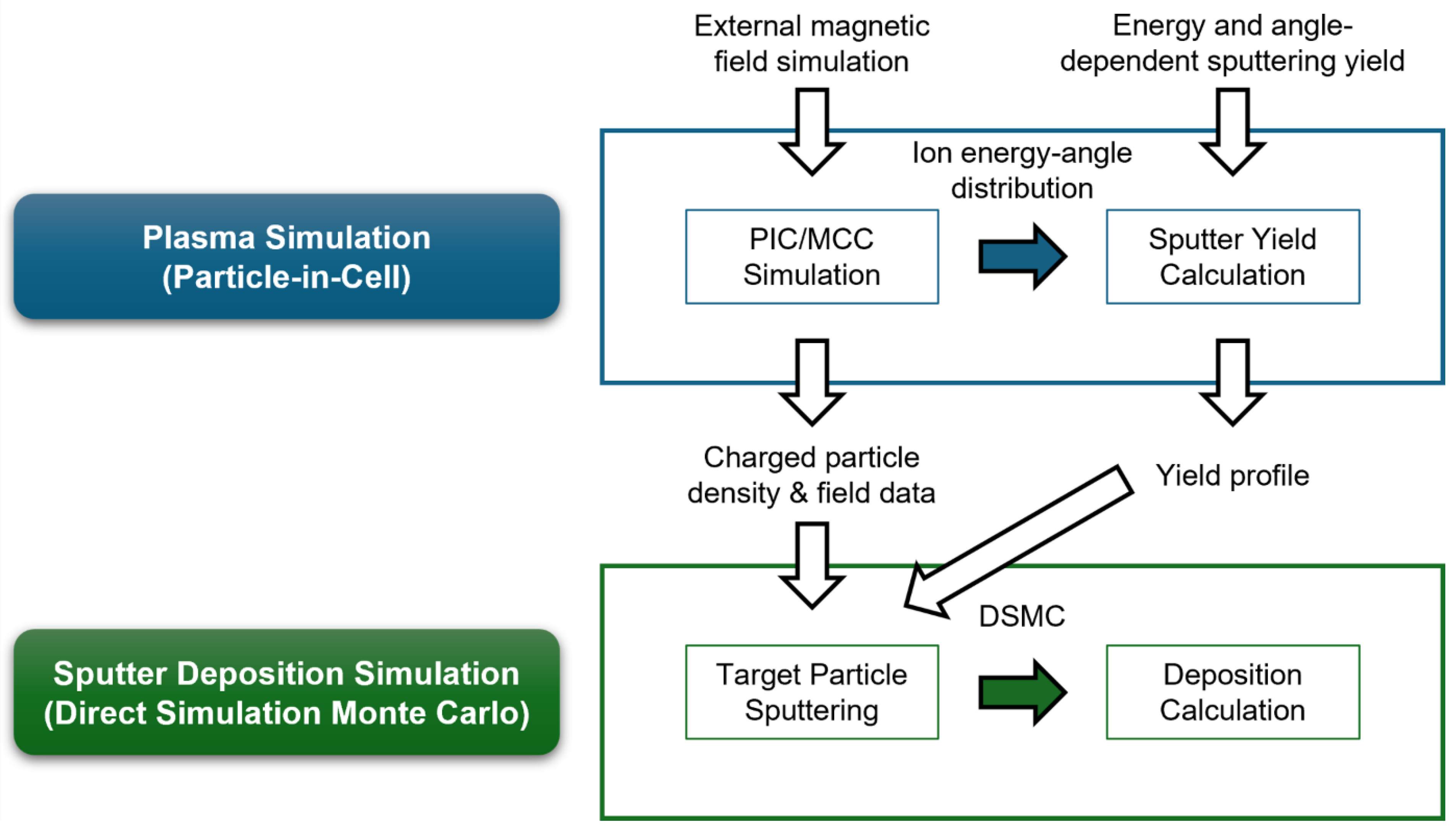
To accurately simulate the magnetron sputtering equipment, three stages of research are required: (i) analysis of the behavior and spatial distribution of plasmas, (ii) analysis of the interaction between ions generated in the plasma and the target surface, and (iii) analysis of the behavior and deposition of neutral/charged gas emitted from the plasmas. To this end, this study performs multi-step simulations with magnetic field calculation, PIC simulation, yield calculation in polar coordinates, direct simulation Monte Carlo (DSMC), and deposition distribution calculation. For the IMPVD process, the spatial distribution analysis of charged and neutral particles is performed by simulating the RF magnetron sputtering source with rotating magnets.
3. DC Magnetron Sputtering System with a Simple Consideration of the Magnet Configuration
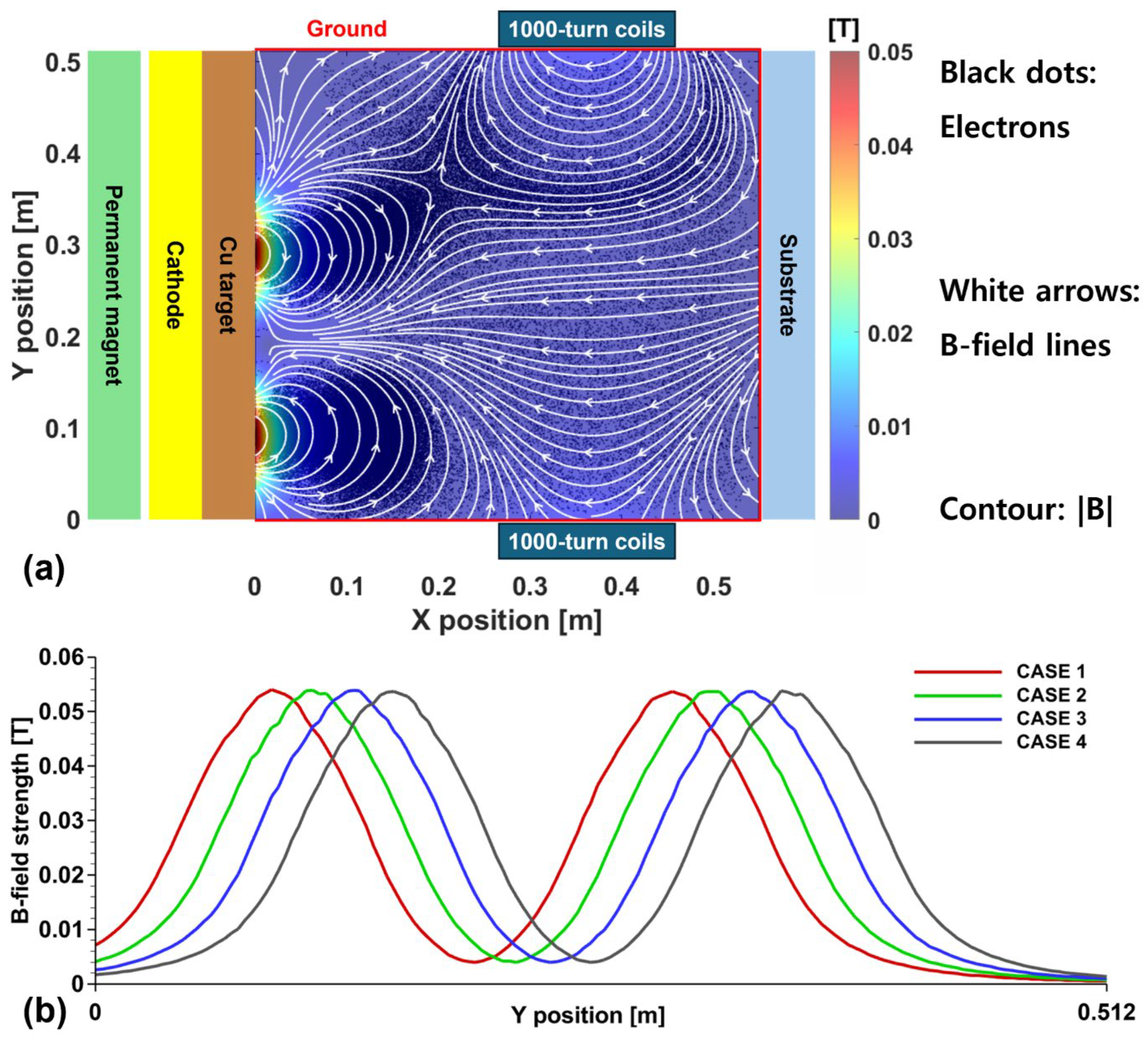
The simulation domain of the DC magnetron sputtering system and the magnetic field intensity distribution, which is obtained by simply shifting the position of the permanent magnet, are shown in
Figure 2. The magnetic field distribution due to the permanent magnets and EM coils was calculated using FEMM. The system size is
, the grid size is
, the time step is
, the gas is argon at
, the DC power is
, and the secondary electron emission coefficient is 0.2.
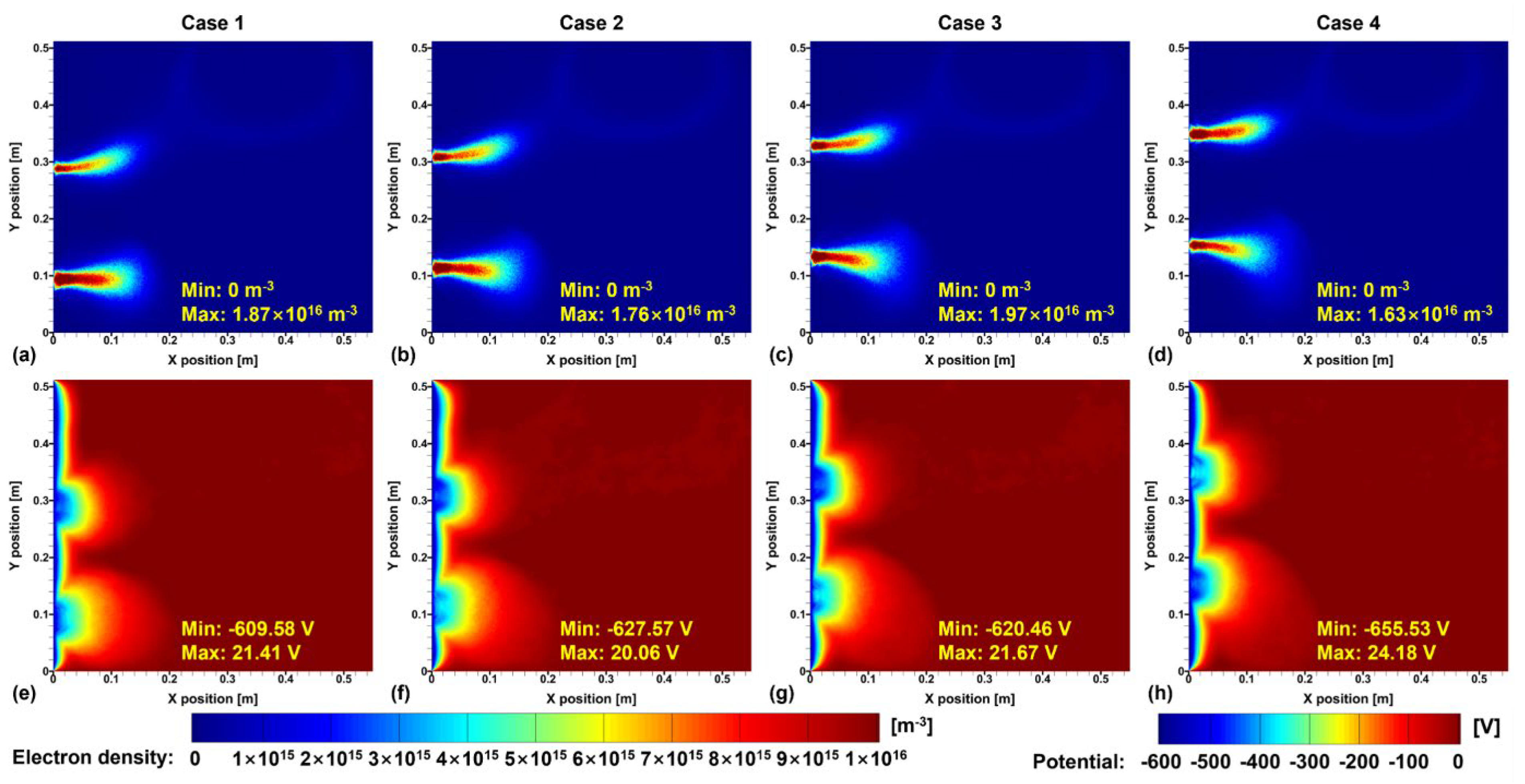
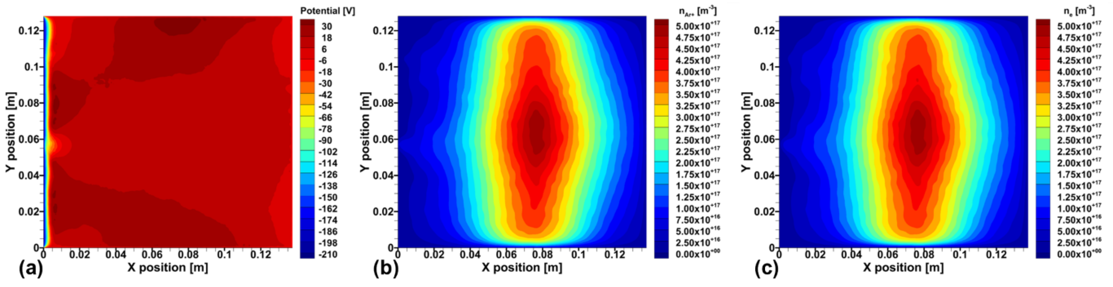
As shown in
Figure 3, electrons are confined in regions with high magnetic field strength. Since these electrons generate ions through ionization in these regions, a plasma formation profile is observed in the areas with higher magnetic field strength. As can be seen from the potential and electron density distributions, the magnetic mirror effect caused by the magnet location at a lower position on the
-axis causes electrons to move toward the ground region at
, resulting in a broader electron distribution profile compared to the electron distribution that is confined by the magnets located at higher positions on the
-axis. Furthermore, the magnetic field formed by the EM coils causes the narrower electron distribution at the higher position on the
-axis. Although the field strength is about 1/10 of that formed by the permanent magnet, it can create an X-point where the field strength becomes zero, which causes the electrons to move toward the EM coils. Magnetic mirror effect is also observed in this region. Therefore, in Case 1-3, the voltage drop is relatively smaller near the magnet located at a lower position on the
-axis, while in Case 4, the voltage drop is relatively smaller near the magnet located at a higher position on the
-axis. In other words, in Case 1-3, electron loss occurs toward the
boundary. In Case 4, however, electron movement due to the closer X-point causes the potential distribution near the permanent magnet to change. The distribution of the strong voltage drop near the target affects the energy and angle of the ions striking the target, and this can be used to calculate the sputtered target particle yield.
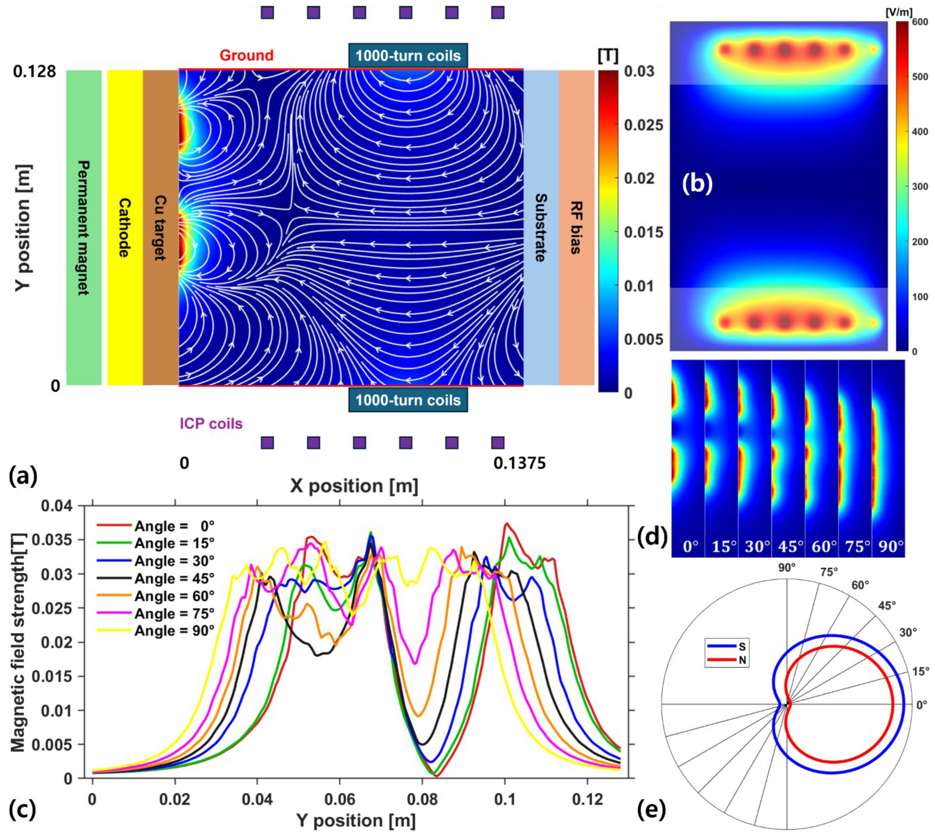
Figure 2.
(a) Schematic DC magnetron sputtering device diagram. The magnetic field strength, flux lines, and electron spatial distribution are shown following the arrangement of permanent magnets and EM coils. (b) Magnetic field strength at the target surface when the position of the magnets is shifted.
Figure 3.
(a-d) Electron density distributions and (e-h) potential distributions for each case.
Figure 3.
(a-d) Electron density distributions and (e-h) potential distributions for each case.
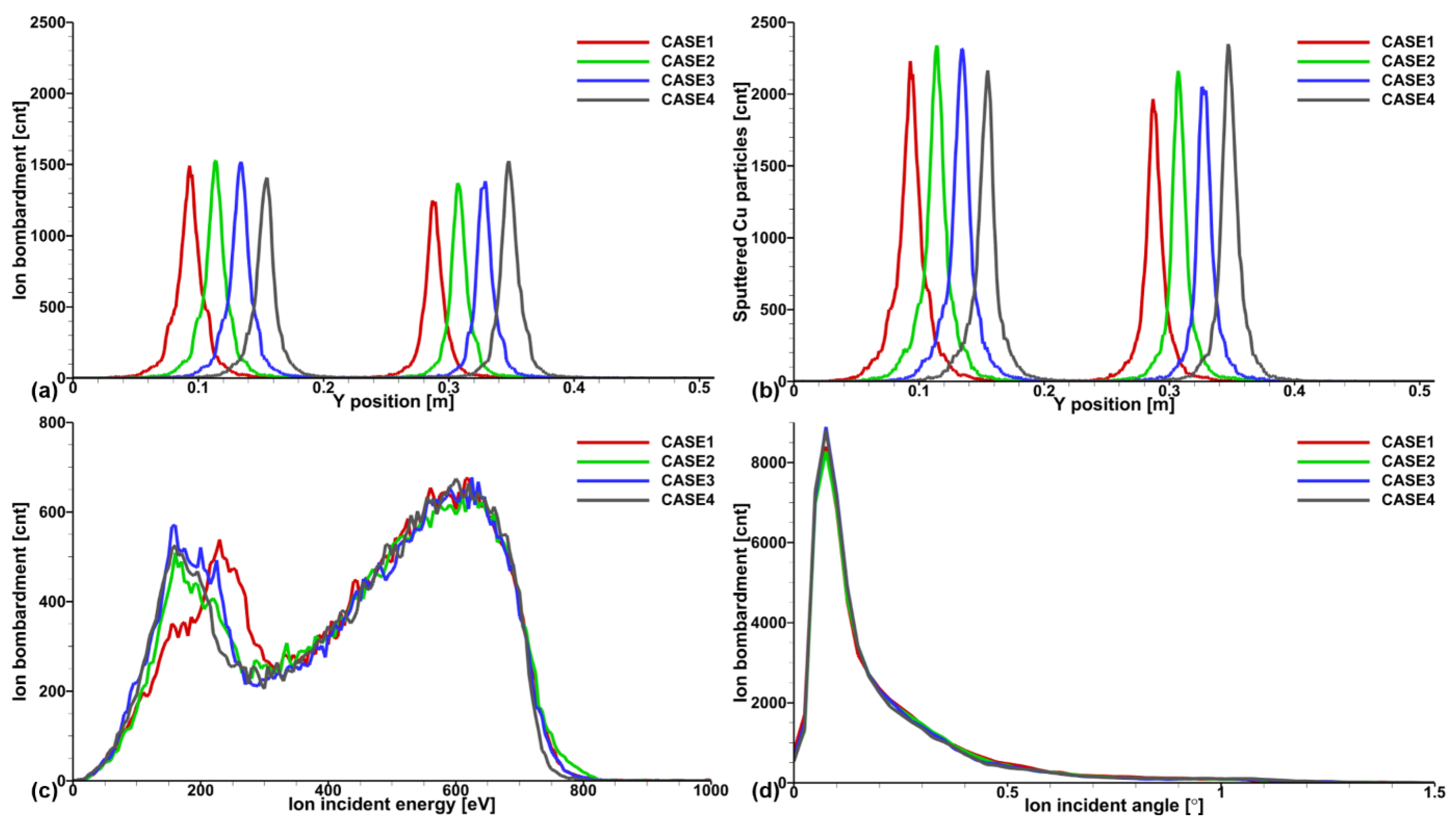
Figure 4.
(a) Ion bombardment incident on the target, (b) amount of sputtered material from the target, (c) amount as a function of ion incident energy, and (d) amount of ion bombardment as a function of incident angle.
Figure 4.
(a) Ion bombardment incident on the target, (b) amount of sputtered material from the target, (c) amount as a function of ion incident energy, and (d) amount of ion bombardment as a function of incident angle.
Figure 4 shows the ion bombardment incident on the
target, the amount of sputtered metal resulting from it, and the energy and angle distributions of the incident ions. The spatial distribution of ions incident on the target is high in the region where the magnets are located due to the higher plasma density, and the magnetic field distribution controls it. The energy of ions striking the target is determined by the potential difference from the ionization region to the target surface, but the incident ion angle does not vary significantly according to the magnetic field distribution. The effect of the voltage drop is much more significant, so most ions have an angle of less than
. Furthermore, due to the collision of high-energy
ions, more than one target particle is sputtered by a single ion.
4. RF Magnetron Sputtering System with the Rotating Magnets
As shown in the simple DC magnetron sputtering results, the incident ion energy contributing to the generation of sputtered metal is affected by the magnetic field distribution and plasma distribution. Yamamura proposed that the yield depends on normal incident ion energy [
24]. Using this, Eckstein proposed a yield incorporating angular dependence [
25,
26]. To calculate the sputter yield dependent on this IEAD, the Yamamura and Eckstein formulae were incorporated into the PIC code. Additionally, the data for calculating the sputtering and reaction of the
target in argon plasma using sputter yield through DSMC is presented in
Table 1.
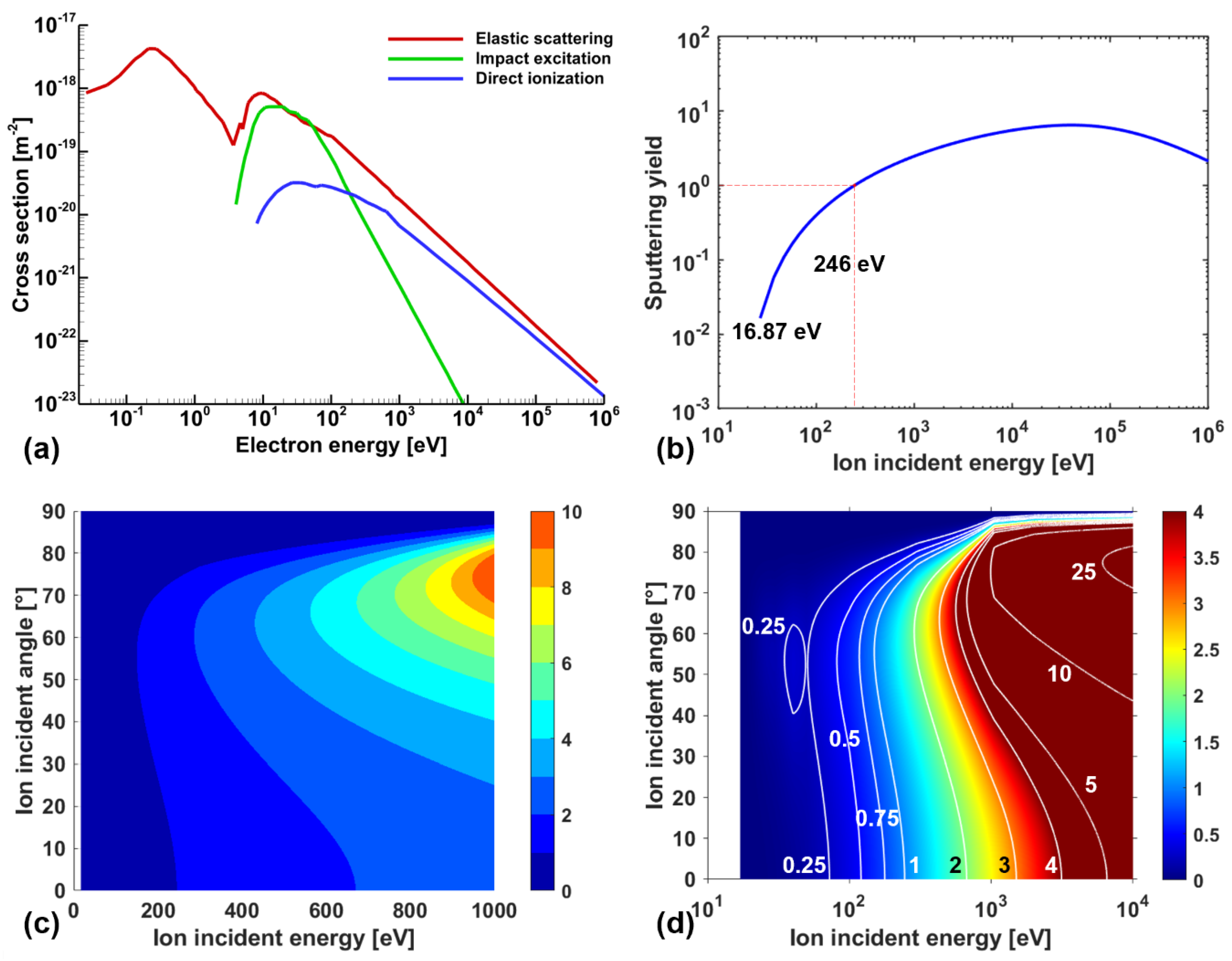
Figure 5.
(a) Collision cross sections of Cu atoms dependent on electron energy, (b) Yamamura formula, and (c-d) Eckstein formula.
Figure 5.
(a) Collision cross sections of Cu atoms dependent on electron energy, (b) Yamamura formula, and (c-d) Eckstein formula.
The cross-sections for the reaction between electrons and copper atoms are shown in
Figure 5a. Additionally,
Figure 5b shows the Yamamura formula, where sputtering occurs only when the ion incident energy exceeds the threshold energy of approximately 16.87 eV. When the normal incident ion energy reaches about 246 eV, the sputtering yield becomes 1.
Figure 5d represents the Eckstein formula considering angular dependency, while
Figure 5c shows the Eckstein formula for the region of interest.
Table 1.
Reaction sets for the plasmas with the target.
Table 1.
Reaction sets for the plasmas with the target.
| Reaction Equation |
Name |
) |
Ref. |
|
Elastic scattering |
1
|
[27] |
|
Electron impact excitation |
1
|
[27] |
|
Direct ionization |
1
|
[27] |
|
Elastic collision |
|
a 2
|
|
Charge exchange |
|
a 2
|
|
Charge exchange |
|
[28] |
|
Elastic collision |
|
a 2
|
Figure 6.
(a) Schematic diagram of the IMPVD device, (b) calculation domain of the ICP coils, (c) magnetic field distribution at the target surface for different rotation angles, (d) Magnetic field distribution near the target for different rotation angles, and (e) symmetry in the cardioid shape magnet configuration.
The schematic diagram of the IMPVD device, where metal particles sputtered from the target are ionized in the high-density plasma and incident perpendicularly onto the wafer by the electric field, achieving higher anisotropy compared to other methods, is shown in
Figure 6a. The magnetic field generated by the cardioid-shaped permanent magnet is calculated using CST. Additionally, a DC bias is applied to collide ion particles from the plasma with the target in order to sputter target particles. An RF ICP is used to generate high-density plasma, and the 6-turn coil is placed to ionize the sputtered metal particles. RF bias is applied to incident ionized target particles perpendicularly onto the wafer. The EM coils near the wafer, which induce the magnetic field to control the position of the incoming metal ions, are calculated using FEMM.
The simulation domain size is , with grid spacing of and a time step of . Argon gas at is used. The ICP is operated at a frequency of with power, a DC bias of or is applied, and an RF bias of with is applied. A current of is passed through the EM coil. Additionally, the side wall is grounded.
Figure 6b shows the electric field in the
-direction generated by the ICP coils. The translucent area represents the region where the electromagnetic field is calculated by considering additional cells outside the PIC simulation domain, while the opaque region is the area where particles are handled.
Figure 6c shows the magnetic field strength on the target surface, extracted from CST calculations at
intervals from
to
. The magnetic field distribution around the target at each angle is shown in
Figure 6d. The reason for considering angles from
to
is that, as shown in
Figure 6e, the results between
and
can be calculated using symmetry.
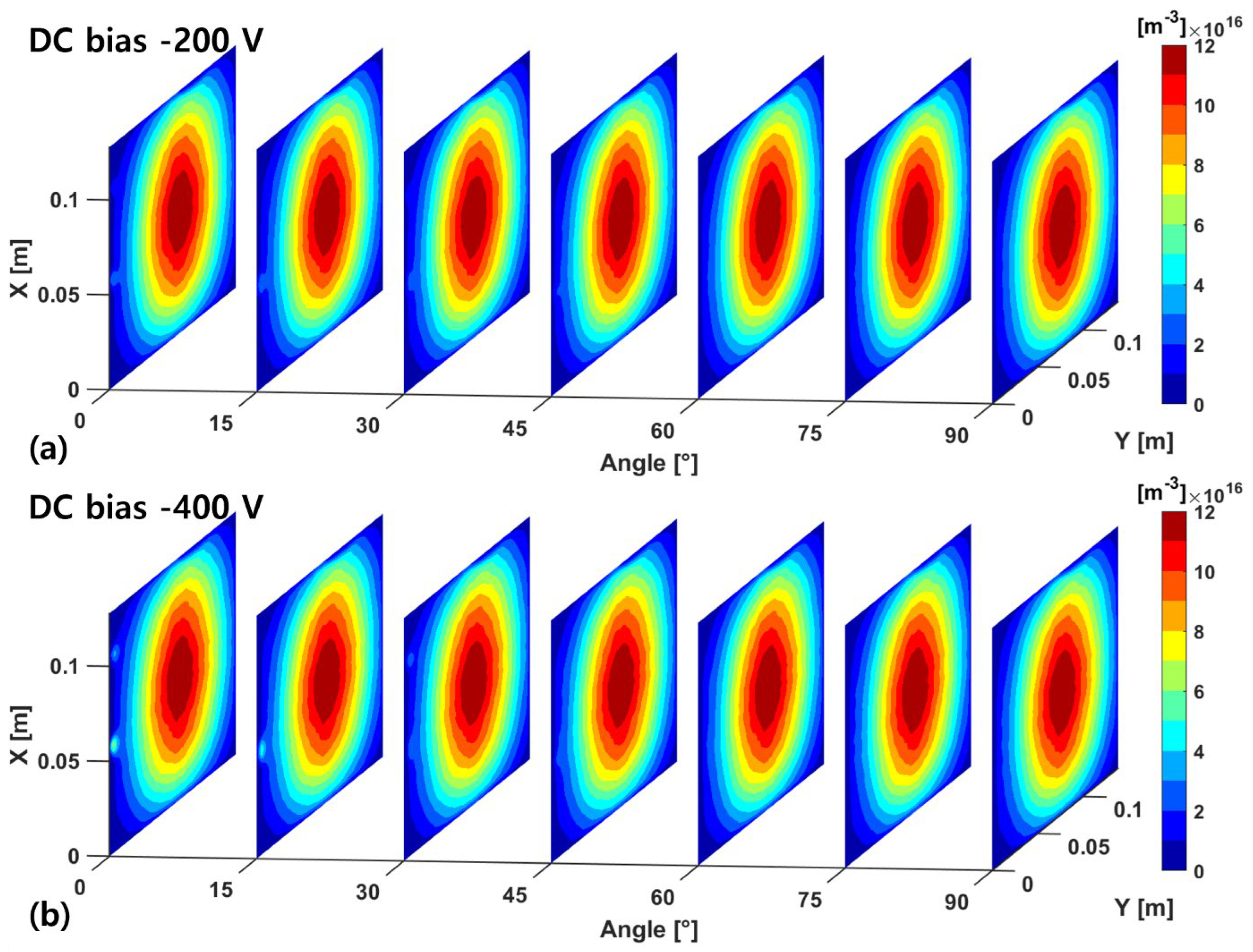
Figure 7.
(a) Argon ion density profiles with a DC bias of -200 V and (b) with a DC bias of -400 V to the different magnetic field angles.
Figure 7.
(a) Argon ion density profiles with a DC bias of -200 V and (b) with a DC bias of -400 V to the different magnetic field angles.
As shown in
Figure 7, the dense plasmas are generated primarily at the center by the ICP source, and the plasma densities slightly increase around the magnets. At -400 V, the plasma densities around the magnets are slightly higher than -200 V. As shown in Figs. 6c and 6d, the magnetic field distribution becomes relatively uniform around
, and plasmas at this angle do not experience an increase in density around the magnets.
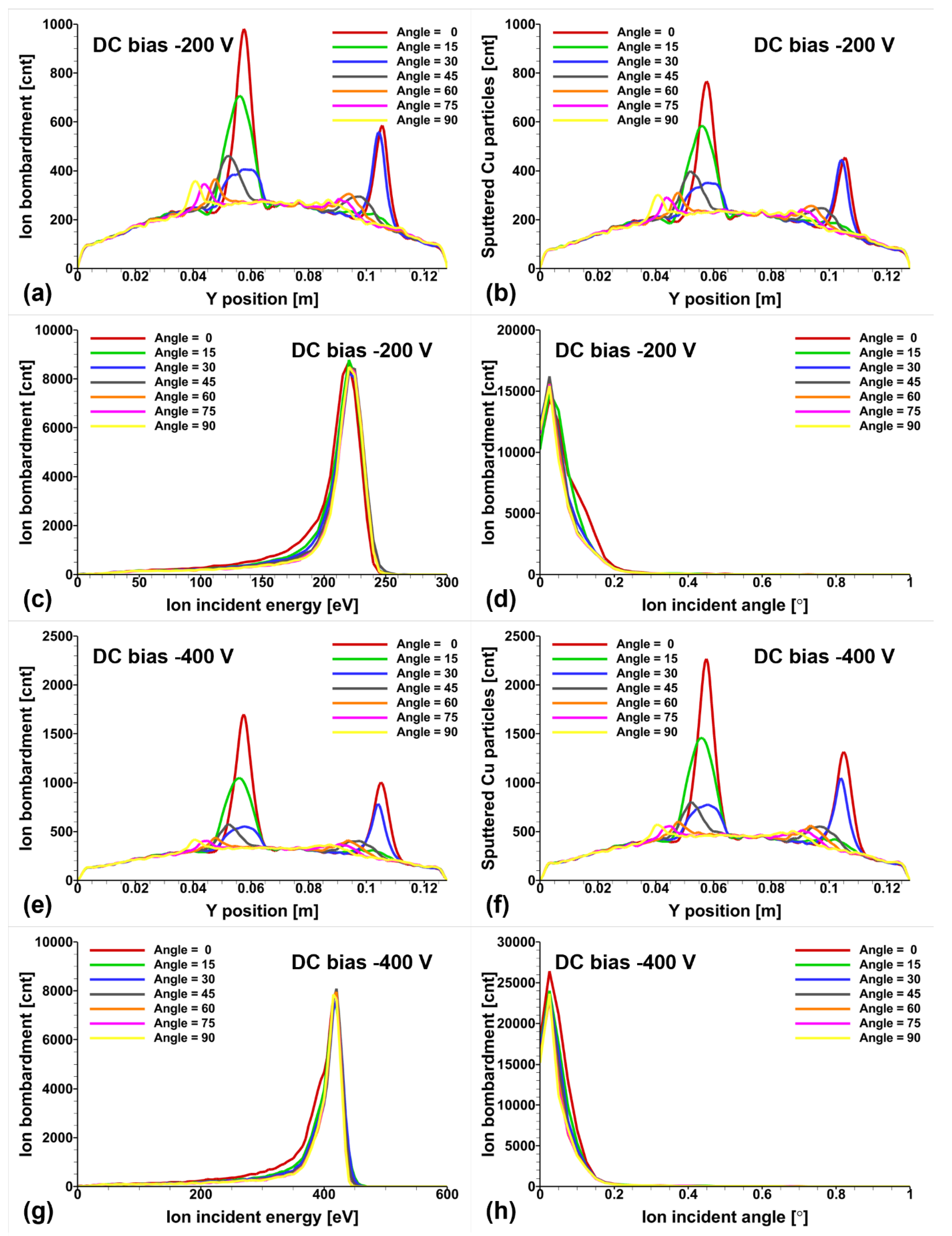
Figure 8.
For DC biases of -200 V and -400 V, ion bombardment distributions with respect to space, sputtered particle distributions with respect to space, ion bombardment distributions with respect to the ion incident energy, and ion bombardment distributions with respect to the ion incident angle.
Figure 8.
For DC biases of -200 V and -400 V, ion bombardment distributions with respect to space, sputtered particle distributions with respect to space, ion bombardment distributions with respect to the ion incident energy, and ion bombardment distributions with respect to the ion incident angle.
Although there seems to be no significant difference between -200 V and -400 V DC bias voltages when only considering plasma density, as shown in
Figure 8, there is a notable difference in the ion incident energy distribution. The ion acceleration due to the difference between the -200 V and -400 V DC bias voltages and the plasma potential results in an incident ion energy distribution that is slightly higher than each bias voltage. As shown in the Yamamura formula in
Figure 5b, for sputtering yield to exceed 1, the argon ion must have an energy greater than 246 eV when incident on the copper target, which leads to a significant difference in sputtering yield. As seen in
Figure 8c, in the -200 V DC bias case, there is not much ion bombardment above 246 eV, resulting in smaller sputtered Cu particles in
Figure 8b compared to ion bombardment in
Figure 8a. In contrast, in the -400 V DC bias case shown in
Figure 8g, there is a higher amount of ion bombardment above 246 eV, leading to larger sputtered
particles in
Figure 8f compared to ion bombardment in
Figure 8e.
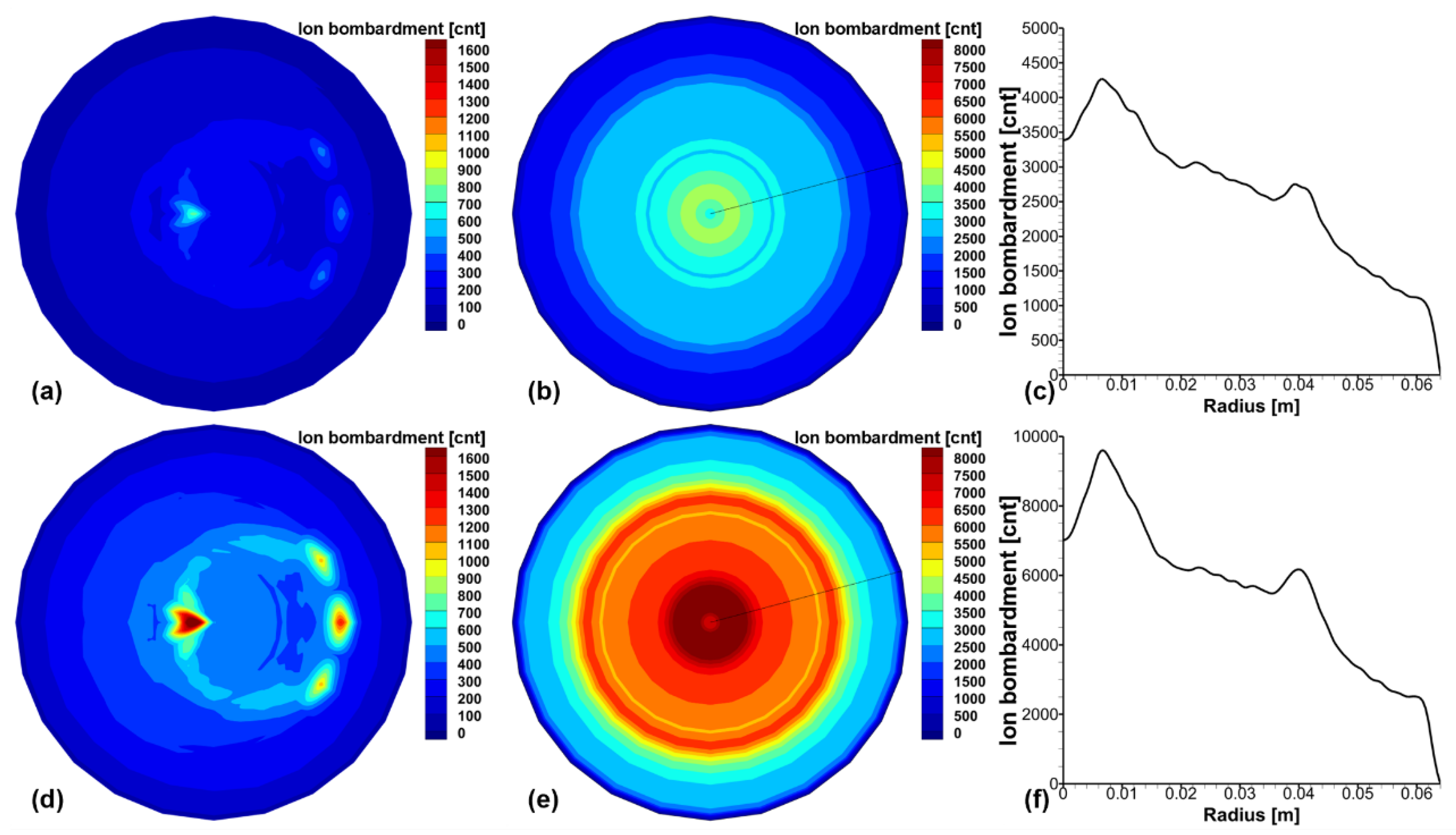
Figure 9.
At -200 V DC bias, (a) ion bombardment on target with a stationary magnet, (b) ion bombardment on target with a rotating magnet, and (c) ion bombardment as a function of radial position. At -400 V DC bias, (d) ion bombardment on target with a stationary magnet, (e) ion bombardment on target with a rotating magnet, and (f) ion bombardment as a function of radial position.
Using the IEAD obtained from
Figure 8, the distribution of the ion bombardment for each angle of the magnet is transformed into a polar coordinate system, as shown in
Figure 9. Rotating
Figure 9a results in
Figure 9b, and the data extracted along the black solid line is shown in
Figure 9c. This calculation is performed because the values of the electric and magnetic fields vary with the rotation angle of the magnet, so the distribution of sputtered particles is calculated separately for each angle. Since the target rotates, this distribution is rotated to make it symmetric. Plasma density and electric and magnetic field data are used as fixed values in the DSMC simulation. This approach helps avoid heavy computations in the 3D field and allows the sputtered particle calculation to be performed in 3D.
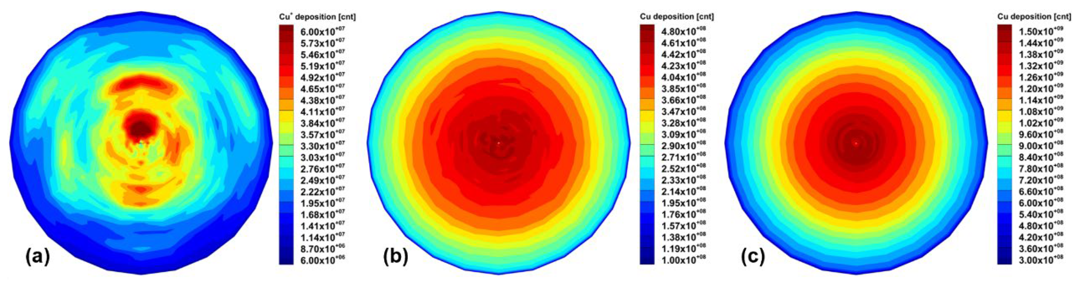
Figure 10.
When the DC bias is -200 V, (a) Cu ions deposited on the substrate, (b) Cu atoms deposited on the substrate, and (c) Cu atoms deposited on the substrate without considering collisions.
Figure 10.
When the DC bias is -200 V, (a) Cu ions deposited on the substrate, (b) Cu atoms deposited on the substrate, and (c) Cu atoms deposited on the substrate without considering collisions.
When comparing
Figure 10b and 10c, it is observed that the number of Cu particles reaching the wafer is relatively smaller when collisions are taken into account. The case considering collisions shows better uniformity compared to the case without collisions. Since Cu particles are neutral, they are unaffected by the EM coil and directly reach the wafer. In the case of Cu ions in
Figure 10a, the amount reaching the wafer is about eight times smaller than the Cu particles. This is because the Cu ions are not sufficiently ionized, as the Ar ion density is relatively low at
. Due to computational limitations, the ICP power was reduced in the simulation, resulting in a low Ar ion density and consequently fewer Cu ions being produced. To better understand the collision rates and the density distribution of each species, it will be necessary to adjust the simulation conditions to increase plasma generation and observe the results.
To simplify the problem, a DC bias of -210 V is applied, and the RF bias is combined with a DC voltage of -20 V and 50 V at a frequency of 2.5 MHz. The distribution of the permanent magnet is set to the same as shown in
Figure 6, but the magnetic field strength is doubled. Under these conditions, EM coils and ICP coils are not used. PIC simulations are first performed, and the resulting potential, as well as the distributions of electrons and argon ions, are shown in
Figure 11.
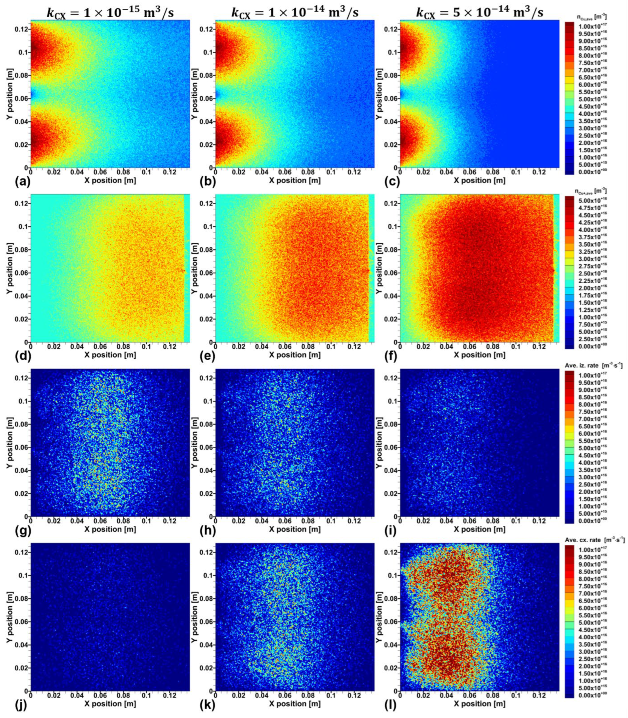
Using these results, simulations are performed by changing the rate coefficient for the charge exchange between Ar ions and Cu atoms, as listed in
Table 1. Three cases with rate coefficients of
,
, and
are considered, and the results of the DSMC simulations are shown in
Figure 12. The higher the rate coefficient for charge exchange, the fewer Cu atoms there are, and the more Cu ions are present. Additionally, when the charge exchange has a higher collision rate, the number of Cu atoms decreases, which is turn reduced the collision rate for ionization.
From this result, it is clear that obtaining accurate cross-section data for the charge exchange reaction is important. Another point to consider is that the simulation of sputtered particles assumes the immobile plasma in the background, meaning that the potential distribution is almost fixed, and as a result, the motion of the generated Cu ions is not accurately represented. Therefore, further research considering the coupling between the plasma and sputtered particles is necessary.