
Submitted:
01 December 2025
Posted:
02 December 2025
You are already at the latest version
Abstract
We review general properties of optical reflection spectra recorded from smooth solid surfaces from the infrared up to the X-ray spectral regions. Emphasis is placed on metal surfaces. Starting from a simple classical oscillator model treatment, general features of normal incidence reflection spectra are derived in a qualitative manner. This rather tutorial approach as relevant for an ideal metal surface is complemented by a broad elaboration of analytical features of realistic reflection spectra. Discussed topics include manageable dispersion formulas, the Kramers-Kronig method, oblique light incidence effects with emphasis on Azzam’s analytical relations between the Fresnel’s coefficients, as well as special spectroscopic configurations involving reflection measurements at grazing light incidence. Among the discussed grazing incidence techniques, emphasis is placed on Infrared Reflection Absorption Spectroscopy IRAS, the Berreman effect, as well as X-ray reflectometry XRR.
Keywords:
reflectance
; metal
; optical constants
; dispersion
; Kramers-Kronig
; surface
; Fresnel coefficients
; spectroscopy
; resonance effect
; enhanced electric field
1. Introduction
Many metals belong to the class of optical materials. The latter may be defined as including any solid or liquid material, employed in the refraction, reflection, absorption, emission, scattering, or diffraction of the ultraviolet, visible, and infrared electromagnetic spectrum, covering the wavelength range between approximately 0.1 to 50 µm. Owing to the presence of free (i.e. conduction) electrons, metals have specific optical properties in a wavelength range from the ultraviolet (UV) up to practically infinitely large wavelength values [1,2,3]. These specific optical properties make them indispensable candidates for use in various kinds of optical coatings [4]. With respect to optical applications, we find metals like aluminum, gold, silver, and chromium among the most frequently used metals in coatings.
In this regard, metals are of primary importance for the design of reflectors, optical transmission filters, neutral density filters, asymmetric beam splitters, decorative coatings [4,5,6], solar absorbers [7], or so-called black reflectors [8]. Often, their unique reflective properties are the feature that is primarily exploited in metal-containing optical coatings [9].
In general, any coating composed from passive materials illuminated by light may primarily transmit, reflect, scatter, or absorb the incident electromagnetic radiation [10]. Here, the absorptance of a sample is defined in physics as the ratio of the absorbed and incident radiation fluxes [3,11,12]. When taking into account the typical model assumptions valid in thin film optics [1,13,14] (particularly the assumption of plane monochromatic waves), we can write this as the ratio of absorbed and incident light intensities [5,6,13,14], i.e.
with – absorbed amount of the light intensity, and – incident light intensity. Correspondingly, we define transmittance , Reflectance , and scatter according to:
(compare Figure 1). Here, the intensity has to be understood as the average energy penetrating a unit area in a relevant time interval.
The focus of the present paper is on the reflectance, and particularly, on the reflectance arising at any single plane interface in a system as shown in Figure 1.
Before turning to some necessary theoretical material, we would like to emphasize that this paper is dedicated to the memory of Ronald Willey, who passed away on January 21st, 2025. Ron was a scientist and teacher all his life, and in his last articles, he developed his own approach to practical design of various metal-containing types of optical coating [7,8,9]. One of the authors of the present paper (O.S.) had the honor to co-author one of these articles [9]. This was in fact the final stimulus for us to write the present paper, with emphasis on the description of the optical properties of metal surfaces, in a style that combines features of a tutorial with those of a review paper. We hope that this provides a relevant frame to honor Ron’s work in a dignified manner.
2. Theoretical Aspects
2.1. First Considerations
In order to comply with the topic of optical coatings in the simplest manner, this study will deal with flat samples only, built from a stratified isotropic medium with a symmetry axis perpendicular to any of the surfaces and interfaces [1,14]. As an example, this could be an optical coating deposited on a flat isotropic substrate (Figure 1).
The most pragmatic choice for optical characterization of such a sample in daily characterization or quality control practice [15] could be to perform a transmission measurement, resulting in a transmission spectrum . Here ω is the angular frequency of the incident light. However, the information obtained from this transmission measurement is incomplete, because it is not clear what happened to the amount of light that is missing in transmission. In fact, the light incident to the sample surface may be transmitted, reflected, absorbed, or scattered. In consistency with energy conservation, we may therefore write:
When restricting to the simple model case when scatter is negligible, from we find the sample absorptance as:
It is immediately clear, that reliable information on the samples absorptance cannot be obtained from transmission measurements only, instead, the sample reflectance has to be measured as well. Already from here it turns out, that reflection measurements are at least equally important in solid state spectroscopy as transmission measurements. We mention in this context the value of reflectance measurements in surface analytics [16] and thin film optics [17,18] alike. In particular, as a result of the large amount of information that may be drawn from reflection spectra, early studies on the use of neural networks in thin film optical recognition tasks make primary use of reflection spectra [19,20,21].
We would like to emphasize two further arguments that magnify the value of reflection measurements. Imagine the situation sketched in Figure 2. On left, light is incident from the top of the sample, giving rise to a certain transmission () and reflection () signal. On the right, the light path is reversed, the light is incident from the bottom, formally giving rise to a transmission signal and a reflection signal . However, as every experienced spectroscopist knows, the transmittance is insensitive to a light path reversal [5,6]. In particular, for the transmission measurement of a single-side coated substrate, it does not matter whether the sample is illuminated from the coated side (here from top), or from the substrate side (here from bottom). Hence, . Thus, reversing the light path in a transmission measurement does not provide any new information.
The situation is different for the reflection measurement. Indeed, from (4) and we immediately obtain:
In any absorbing sample, this allows the reflectance measured from top and bottom sides to be different from each other. Hence, in a reflection measurement, light path reversal (a sample turn in practice) may provide new information. This is a principal advantage of reflection measurements compared to transmission measurements.
This leads us to an interesting conclusion. Let us measure a sample transmittance of 0.2 (i.e. 20%). From this measurement alone, we cannot conclude on the presence of absorption in the sample, because the remaining 80% may have been reflected. Of course, the situation is the same for a single reflection measurement.
However, if two reflection spectra recorded from top () and bottom () are available, further conclusions may be drawn. Provided that the is different from , from (5a) we immediately find:
But that means, that at least one of the absorptances and must be different from zero. Hence, a sample, that shows different reflection from top or bottom, must necessarily contain absorbing fractions. Or even without a spectrometer: when the color appearance from both sample sides is different, the sample must be absorbing in the visible spectral range (VIS).
We would like to provide a second argument for the use of reflection measurements. Imagine the situation of a completely intransparent sample. This could be a coating on a silicon wafer in the VIS. The VIS transmittance is clearly zero, hence a transmission measurement makes no sense at all (Figure 3).
Nevertheless, a reflection signal will be available anyway (the only exclusion would be a perfect absorber), it is at least the sample surface (highlighted by the red ellipse) that usually provides a reflection signal, which still carries information about the properties of the sample material. Hence, reflection measurements are indispensable in the analytics of intransparent samples. In special cases, the sample reflectance of a strongly absorbing sample may coincide with the reflection spectrum of the single sample surface.
From here we postulate the composition of the simple model system that will accompany us through section 2 and parts of section 3 of this study. In the forthcoming, we will restrict on certain features of a reflection spectrum obtained from the surface between vacuum (or air) and an optically homogeneous and isotropic non-magnetic material, recorded at normal incidence (Figure 4 on left).
2.2. The Reflection of a Single Interface at Normal Incidence
Let us assume a smooth plane interface between a damping-free incidence medium (medium 1) and a second medium (medium 2), that may show some damping (Figure 4).
Provided that both media are optically isotropic, we write their complex indices of refraction as:
Here, , , and are real numbers. The -values correspond to the usual real refractive indices, while is the extinction coefficient, here of the second medium. For non-magnetic materials, the complex index of refraction is related to the complex dielectric function via [1,2,15]:
The normal incidence (Figure 4 on left) reflectance at the interface may be calculated as a special case of Fresnel’s formulae according to:
Note that the reflectance is 1 (or 100%) whenever holds. This extreme model situation describes what may be called an ideal metal, such that (9) predicts a large reflectance of light at metal surfaces. If the light is incident from vacuum (or with good accuracy from air), from (9) we quickly obtain the simpler relation:
Figure 5 and Figure 6 show examples of different normal incidence reflection spectra at air-metal interfaces (Figure 5) and air-dielectric (or semiconductor) interfaces (Figure 6). The reflectance’s have been calculated by means of (10) making use of optical constants of metals as implemented in the UNIGIT database [22]. For the other materials, data available at [23] based on data from [24,25,26] have been used.
Let us mention three important empirical findings:
- For , the reflectance approaches zero. This is observed in metals and dielectrics (or semiconductors) alike.
- For , the reflectance of all metals approaches one. This is different to the behaviour of dielectrics.
- In the UV/VIS/IR spectral regions, the reflectance of several materials shows specific spectral features as characteristic to resonances.
2.3. A Simple Oscillator Model Approach
This section forms the basic tutorial part of this study. We will present a simple model that qualitatively explains the phenomenological characteristics found in the reflection spectra from Figure 5 and Figure 6. The basic idea is that the electric field in the electromagnetic wave results in the formation of induced microscopic dipoles, which oscillate with the frequency of the wave. In order to relate those dipole moments to our reflection spectra, we will simply assume, that a vanishing amplitude of the oscillating dipole moment corresponds to a vanishing interaction of light with matter. In this case, the wave propagates through the medium similarly like through vacuum. Correspondingly, , and therefore, according to (4), . On the contrary, when the oscillation amplitude of the induced dipole becomes very large, the light-matter interaction is strong, such that we expect relevant features in the reflection spectrum and, in particular, a large reflectance.
Let us assume now an oscillation of a dipole formed from a positive (+) and a negative (-) charge separated from each other by a distance . Then, the dipole moment is . In our model, and according to Figure 7, the dipole shall now be modeled by a mass-on-a-spring system [27]:
In order to avoid complex calculus at this stage, in this model we will further neglect any damping, such that from Newtons law we find:
Where F denotes forces, m the reduced mass of the considered two-bodies system, and a the acceleration.
When setting , (κ is the spring constant), we obtain the equation of motion:
Here is the electric field strength in the incident light wave. Assuming a monochromatic incident wave, the ansatz ; quickly results in the solution:
Therefore, we obtain the oscillating dipole moment according to:
Let us now look what can be learned from this simple relation.
MIR/VIS/UV response:
Let us have a look at the conditions when this dipole moment may become very large. Once and are given values, the only possibilities for a diverging (or very large) dipole moment are
- A practically infinitively large electric field or
- A vanishing denominator in (11) and (12).
Hence:
Condition a) seems exotic, but in fact there are spectroscopic (interface-sensitive) techniques that gain their sensitivity from sufficiently large by amplitude oscillating electric fields near the interface [28,29]. This is rather obvious at structured metal surfaces, but even in the vicinity of a plane metal surface, may become rather large at oblique incidence. Once at the moment we are discussing normal incidence, we will not go into details here, but will return to them later in Sect. 3.2. Moreover, in any microscopic theory, the field in (12) has to be associated with the local electric field in the spatial vicinity of the considered dipole, which is not necessarily identical to the field in the incident wave [15,30,31].
Let us now elaborate condition b).
In the simplest classical non-relativistic picture, when regarding an electron oscillating around a heavy (positively charged) nucleus, the value equals the negative elementary charge , while practically coincides with the electron rest mass . Hence,
The specific situation in real metals is characterized by the coexistence of both bound and free electrons. Note that in our classical model, corresponds to a free electron, while corresponds to bound electrons. Let us therefore discriminate between these situations. We have:
Therefore, for free electrons, according to (12) we find the dipole moment according to:
This expression is obviously independent on the concrete metal. When accepting the rule: large dipole moment <=> strong reflectance, it explains the converging behavior of the normal incidence reflectance of different metals at smallest frequencies (compare Figure 5 and (16)). For bound electrons, instead, we obtain resonant behavior at . Once the resonance frequencies depend on the assumed spring constant and are therefore material-dependent, spectral features in the reflection spectrum caused by the optical response of bound electrons appear to be material- and frequency-dependent. For reasonable spring constants and the rather small electron mass, those features usually fall into the VIS/UV spectral regions (compare Figure 5) [1]. In particular, the response of bound electrons is responsible for the specific color appearance of several metals.
Note than in the energy band model resulting from a quantum mechanical treatment, optical excitations of free electrons are associated with intraband transitions, while those of bound electrons with interband transitions [32,33].
Let us shortly discuss the reflection spectrum of dielectrics in terms of this model. Once in ideal dielectrics, there are no free charge carriers, we only have to consider the situation of . For from (12) we find:
This results in finite values of the dipole moments, which depend on the assumed spring constants and are therefore specific for a given material. In terms of our assumed relation between the dipole moment and the reflectance, we have to expect different values of the reflectance of different materials. This is exactly what we have observed in Figure 6.
Prominent structures in the reflectance of dielectrics therefore occur only at resonance, i.e. at . Electronic resonances are again observed in the UV/VIS spectral ranges (compare Figure 6), while the vibrations of the much heavier atomic cores (a larger in (12)) in ionic crystals are excited in the middle infrared MIR and cause what is called a reststrahlen band in the reflection spectrum [31]. Note that reststrahlen band optical absorption may be excited in elemental crystals as well, but only if more than 2 atoms are incorporated into the primitive cell of the crystal structure [34]. The primitive cell of the silicon lattice contains only two atoms, and therefore, in Figure 6, no reststrahlen absorption is observed.
The behaviour at :
At largest frequencies, from (12) we find the same asymptotic behavior for both free and bound charge carriers alike according to [2]:
This is a physically transparent result, because at largest frequencies, no charge carrier with a given rest mass larger than zero can follow the fast oscillations of the field. Hence the electromagnetic wave propagates through the medium without remarkable interaction, which explains the relative transparency of matter with regard to X-ray and γ-radiation. Correspondingly, the reflectance is expected to approach the value zero, no matter whether we deal with free or bound electrons. In terms of our model, this explains the identical behavior of the reflectance of metals and dielectrics (Figurs 5 and 6) for .
It is possible to link our simple microscopic oscillator model directly to reflectance spectra described by the formulas (6) – (10) in Sect. 2.2. Neglecting for simplicity differences between the local and average electric fields (for more sophisticated treatments compare [30,31]), we can write:
Here, is the concentration of induced dipoles in the second medium, and the square of the plasma angular frequency according to the usual definition [15,29]:
Figure 8 presents model calculations of normal incidence reflectance spectra obtained from these simple relations. The spectrum shown on top of the figure corresponds to the case of only free charge carriers (Drude metal), i.e. . It may serve as a model for the reflectance of metal surfaces at small frequencies (Figure 5). It naturally demonstrates the well-known fact, that a plasma reflects light of all frequencies smaller than the plasma frequency. On the contrary, the image in the center of the figure corresponds to . It gives rise to a single resonance frequency (single-oscillator model) and provides an idealized reproduction of local reflectance maxima of bound electrons at resonance. On bottom, (20) has been generalized to the case of 2 resonance frequencies, corresponding to the existence of groups of bound charge carriers differing in their bonding strength, i.e. in the assumed (multi-oscillator model). Because of the assumed absence of damping, all the spectra appear idealized compared to the spectra shown in Figure 5 and Figure 6, nevertheless they reproduce the basic empirical findings as summarized at the end of Sect. 2.2.
Let us emphasize that according to (20), it may turn out that is observed. Indeed, for sufficiently large angular frequencies, we obtain:
The phase velocity [35] of the propagating wave is therefore:
With – velocity of light in vacuum. This might seem to contradict relativity. However, signals are transferred with so-called group velocity rather than with the phase velocity [35]. A short calculation shows, that for the particular dispersion behavior used in (20), becomes:
This relation provides no superluminal signal transfer, and therefore, no conflict with relativity occurs at this point.
2.4. More General Dispersion Formulas
When looking at relation (20)
We recognize at least two shortcomings:
- Relation (20) does not suffice thermodynamics, because relaxation is excluded
- At resonance, shows a singularity, that is not observed in reality
Therefore, in practice our oscillator as introduced in Sect. 2.3 has to be replaced by a damped oscillator. Then, instead of (20), we obtain a complex dielectric function of an assembly of oscillators according to [1].
with – damping constant. Note that a finite value of results in the emergence of a positive imaginary part of the dielectric function. Thereby, the imaginary part of the dielectric function is responsible for energy dissipation caused by light absorption in the medium. No dissipation occurs when the damping constant is equal to zero. For the response of free electrons (), we have the Drude function [1]:
An early implementation of the classical relations (23) and (24) into thin film calculation routines has been reported by Dobrowolski et al [36].
Note that for , (24) provides a normal incidence reflectance of a metal surface according to the Hagen-Rubens formula:
Where is the static electric conductivity of the medium.
Obviously, according to (25), approaches a reflectance of 1 regardless on the chosen material, again in consistency with the behavior illustrated in Figure 5.
In a quantum mechanical treatment, (23) has to be replaced by a quantum mechanical dispersion formula (compare for example [37]). The classical formulas (24) and (25) as well as the more specific for metals Lindhard formula are obtained as particular cases from that more general treatment [33,37,38]. Although a quantum mechanical treatment is usually not so illustrative, some analogy to our classical picture may be formulated. Thus, in our classical picture, prominent spectral features in reflectance are expected when the induced dipole moments become extraordinary large. In quantum mechanics of crystals, instead, it is the appearance of critical points (van Hove singularities) in the joint density of electronic states that gives rise to characteristic spectral features [31]. A corresponding elaboration of the reflection spectra of metals like Ag, Cu, or Al can be found in the studies of Ehrenreich [16,39,40]. An elaboration of metal spectra in terms of the classical relations (23) and (24) is reported in [41].
2.5. Oblique Incidence
Let us start this section with the remark, that the reflectance according to (2) corresponds to the definition (compare Sect.1):
It is thus defined as the ratio between two light intensities and may therefore be called the intensity reflectance. Note that is a real quantity. It is the quantity that may be measured by means of a spectrophotometer (we will return to this question later in Sect. 2.6), and it provides access to the electric field real amplitude relations in the reflected and incident electromagnetic waves. However, it does not contain any information about the phase relations between the fields in the corresponding waves.
In order to quantify both amplitude and phase information, one may introduce (complex) the electric field reflection coefficient (Fresnel coefficients) using the corresponding electric field strength’s according to:
Clearly [15],
Hence, according to (27), knowledge of provides access to , but not vice versa. Therefore, in the basic theory, one first has to calculate , before getting access to . For the two basic assumed linear light polarizations (s- and p-polarization [15]), the corresponding electric field reflection coefficients are given by the Fresnel formulas (here written in the Mueller convention [42]) according to:
With - angle of incidence, and - angle of refraction.
As it has been pointed out by Azzam, there exist general relationships between the field reflection coefficients at a single interface at s- and p-polarization [15,43]:
Where is defined through:
Obviously, regardless of the assumed refractive indices, from (28) we find:
The latter result is known as the Abeles-condition [43]. From (29) and (30) we learn:
For real refractive indices, (31) coincides with the so-called Brewsters angle. In this case, (29) and (30) together yield:
In other words, at the Brewsters angle, no p-polarized light will be reflected, as long as the imaginary part of any of the refractive indices is negligible (Brewster effect) [15]. Because of the complex nature of the refractive indices of metals, the Brewster effect is relevant for dielectrics with negligible losses only. A model calculation of the angular dependence of the reflectance of an air-metal surface is presented in Figure 9. Instead of the Brewster effect, we merely observe a local minimum in the reflectance of p-polarized light.
2.6. Short Survey of Derived Experimental Techniques
2.6.1. Phase Reconstruction by Means of the Kramers-Kronig Formula
Generally, according to (27), knowledge of the reflectance R at a certain light frequency does not provide direct access to the phase of the complex field reflection coefficient, but only to its absolute value . On the other hand, we have:
Which makes it possible to calculate through a Kramers-Kronig transformation provided that is known at any frequency. We then have [44]:
Here VP denotes Cauchy’s principal value of the improper integral.
In practice, of course, is known only in a limited spectral region, which limits the accuracy of applying (35) in practical applications. Another particular problem may occur when an oblique incidence reflectance at p-polarization is investigated. Then, because of the dispersion of the refractive index, , which may result in additional poles in (35) because of the Brewsters effect. In this case, additional terms (so-called Blaschke products) have to be included into (35), such a procedure is described in [45].
2.6.2. Cavity Ringdown Decay
Cavity ringdown decay (CRD) was developed as a highly sensitive method for measuring absorption with pulsed laser sources. The technique is based on measuring the absorption rate of a laser pulse enclosed in an optical resonator. The light intensity within the resonator decreases exponentially and is caused by various loss contributions due to absorption and scattering at the mirrors of the resonator and the medium between them [46]. Precursor to this method can be found at [47,48,49]. In these cases, the decay time in a cavity has been already used for reflectivity measurements. The method represents sophisticated development of the phase shift method for measuring photon lifetime and reflection in an optical resonator [50]. In the originally published version, it allows very simple loss measurement on the enclosed medium and on the mirrors used. By replacing a mirror within the resonator, it is therefore easy to perform a relative measurement of the reflectivity of a mirror. The identical, curved mirror shape of the mirror to be measured and an average perpendicular incidence of light are practical limitations that suggest an adapted beam path. Nowadays, a folded beam path [51] with a simple flip mechanism allows absolute measurement at oblique light incidence. The measurement method is now widely used, and a standardized procedure in accordance with ISO 13142 [52] is available for the precise determination of high transmission and high reflection values.
For super-highly reflective mirrors (R > 99.999%), random optical loss fluctuation caused by particle intervention in the beam path inside the cavity are limiting the precision and need to be filtered out. In [53] a combination of fixed and variable length cavities has been used to precisely measure a reflectance of 99.99956% with a remaining uncertainty of only 0.2 ppm.
Other modifications to the beam path also allow measurements on fibers [54,55], polarimetric measurements [56], or spatially resolved measurements [57]. The method can also be extended to cw lasers [58]. A brief overview of additional applications and methods can be found in [59]. Combining Cavity-Ring-Down with conventional methods improves the accuracy of reflection measurement, even when the reflectance values are significantly below the specified threshold of 99% in ISO 13142 [52] and the time constant of the exponential decay is therefore too low for the conventional approach [60].
Further information on this method and other developments can be found, for example, in the frequently cited review article [61].
2.6.3. Imaging Spectroscopic Reflectometry ISR
So far it has implicitly been assumed, that the surface investigated shows lateral optical isotropic and homogeneous properties. In the case of real samples, this is not necessarily fulfilled, so that in the past, correspondingly modified characterization techniques have been developed to pursue this circle of problems. This and the next subsections will shortly address this topic.
Let us start with in-plane inhomogeneous samples. Instead of a single reflection measurement, it is now a lateral reflection mapping of the surface that has to be performed. This is what is done in imaging spectroscopic reflectometry ISR (compare [62]). This technique is applicable to laterally inhomogeneous surfaces and laterally inhomogeneous dielectric films. The large amount of input data requires sophisticated data processing techniques to guarantee an efficient surface characterization [63]. Specific applications include – despite of inhomogeneous films and artificially patterned surfaces – the surfaces of biological or medical objects. Closer to the topic of this study, we also mention successful applications of ISR to the characterization of discontinuous gold films [64].
2.6.4. Reflectance Anisotropy Spectroscopy RAS
Finally, because of surface reconstruction phenomena, the isotropy of optically isotropic crystals may be violated at their surface. This may be investigated by means of reflection anisotropy spectroscopy RAS [65]. The method is also known as Reflectance Difference Spectroscopy RDS.
Basically, the idea of the method is in the measurement of two (nearly) normal incidence reflection spectra with different linear polarization directions. It may thus be understood as some kind of normal incidence polarimetry. Because of surface reconstruction phenomena, RAS signals may be detected even from cubic (i.e. bulk optically isotropic) crystals.
Modern applications concern the in-situ control of epitaxial growth [66].
3. Selected Applications
3.1. Measurement Aspects of R
Spectrophotometric measurement of specular transmission and reflection is a very common method for characterizing solid surfaces and thin films [67]. The performance of the spectrometers used for this purpose depends on the technical parameters of the light source(s) and detector(s). The specific selection of suitable components depends on the spectral range, the required spectral resolution, the dynamic [68] and linearity range, the desired measurement speed, the required signal-to-noise ratio, the budget, and many other aspects [69,70,71], which are not covered here.
Systematic errors caused by deviation of the linearity of the response are critical [72,73] and can be observed for CCD arrays [74] and photodiodes [75,76,77], while photomultiplier tubes commonly show a quite good linearity [78]. Deviations from linearity can be detected for instance by variable aperture measurements [79].
This section focuses on the different experimental techniques for reflection measurement and more general aspects of spectrophotometric measurements.
In spectrophotometric measurement, deviations from the assumed sample position led to changes in the position of the light spot to be detected. These are usually greater in reflection than in transmission. For example, even a slight tilt of a substrate leads to a change in the actual angle of incidence by this tilt angle. While in transmission only a lateral offset and no change in direction can be observed, in reflection a change in direction by twice the tilt angle occurs. For this reason, precise reflection measurement on a sample is significantly more difficult than transmission measurement and is the subject of the following notes. A general approach to reducing the sensitivity of the measurement to deviations of the beam path from its ideal position on the detector is to ensure that the homogeneously illuminated area on the sample and the sensitive area of the detector differ in size [80]. To improve the homogeneity of the light source and the detector, the use of an integrating sphere is a common method [81], but it leads to a significant reduction in light throughput [82,83] and thus to a poorer signal-to-noise ratio.
The sample geometry commonly used corresponds to the standard model of solid surfaces and thin films [13] and is designed for parallel, flat interfaces. Experimental solutions for deviating geometries are possible in principle but will not be discussed in detail here. As already outlined in Sect. 2.5, the intensity ratio of reflected and incidence light (see Figure 1) is relevant for the photometric quantities. When recording the intensities, suitable detectors (photodiodes, avalanche photodiodes, multi-pixel photon counters, photomultiplier tubes, image sensors, …) convert the intensity signal into an electrical signal. Potential contributions to the recorded measurement signal from extraneous light and electronic offsets of the detectors can be considered by measuring the dark signal . Thereby, the measurement beam is switched off or blocked and subtracted from the actual intensity signals:
For the measurement of photometric quantities, either dispersive spectrometers or Fourier transform spectrometers are used. In the former, a spatial distribution of the light is achieved by means of a dispersive element (grating, prism, etc.) and the spectral dependence is recorded individually for the wavelengths. In scanning spectrometers, this is done sequentially, but simultaneous detection is also possible using detector arrays. In Fourier transform spectrometers, on the other hand, the spectral dependence is calculated from the recorded interferogram. Here, the simultaneous detection of all wavelengths results in a high measurement speed. Due to the underlying principle, the abscissa accuracy is very high, but good ordinate accuracy is difficult to achieve [84]. An overview of potential sources of error in the implementation of the Fourier transform principle can be found, for example, in [85]. The application of Fourier-transform spectrometers is mainly in the infrared spectral range (FTIR), where it has largely replaced dispersive spectrometers due to its significantly more compact design. The principles of reflection measurement described below are almost independent of the specific operating principle of the spectrometer.
There are different variants of dispersive spectrometers. If the monochromator realized by the dispersive element is located in front of the sample, the measurement is monochromatic [86]. In a flexible, modular design, the monochromator can be designed as part of the basic device. Due to the associated cost advantage, this approach is widely used. If the monochromator is positioned behind the sample, this is referred to as a polychromatic measurement [86]. This has the advantage that any extraneous light in the sample chamber is reduced by the monochromator and does not fully reach the detector, which is usually broadband sensitive.
Another difference between dispersive spectrometers is the use of a reference beam. Single-beam spectrometers do not have this and do not compensate for fluctuations in the intensity of the light source. They are therefore less expensive but typically also less accurate. In contrast, fluctuations in the light source can be largely compensated for in the more expensive dual-beam spectrometers, which are available from various suppliers for demanding measurements. In dual-beam spectrometers, an additional reference beam is generated for this purpose. To do this, the measuring beam is split either spatially by a beam splitter or temporally (and spatially) by a chopper wheel. The fluctuations in the light source led to identical temporal fluctuations in the sample and reference beams and can therefore be compensated for by measuring the intensity of both beams. If a beam splitter is used, a second, ideally identical detector is required, and the total intensity is divided between both detectors. This results in a poorer signal-to-noise ratio and can be avoided by using a chopper wheel to provide the reference beam. However, the measurement must now be synchronized with the chopper wheel movement, and the beam guidance is also somewhat more complex. On the other hand, the full intensity of the light source is available for the respective measurements, and the same detector can be used for both measurements. For this reason, this variant is often preferred.
When implementing the dual-beam principle, it is also common to assume that dark signals remain constant over time. Based on this assumption, the following sequence of measurements has become established (Table 1) [86]. First, during the so-called “auto zero” phase, the “100%” and (optionally) “0%” measurements are performed for the sample and reference beams, and the intensities specified in Table 1 are recorded. For each sample, only the intensities for the sample and reference beams in the corresponding measurement geometry are recorded, and the data from the “auto zero” is considered to be valid for a device-specific duration. This measurement is only repeated after the (assumed) validity period has expired.
The calculation formula for reflectivity is as follows:
The respective measurement times for the intensities in the sample and reference beams are so close together (determined by the chopper speed) that any relevant drift can be ruled out, or they even coincide when a beam splitter and two detectors are used.
There are numerous established approaches to reflection measurement. The simplest option is a relative measurement against a reference mirror (Figure 10). It is obvious, that in reflection the spatial intensity distribution of the light source (symbolized by “L” on the light path) arrives at the detector in a mirror-inverted manner.
For the “auto zero” measurement (Figure 10 (a)), a reference mirror with known reflectance is placed at the sample position. This means, that for the “100%” measurement instead of the intensity now the intensity is recorded. Similarly, for the “0%” measurement the intensity is recorded. For this reason, the value displayed by the spectrometer must be multiplied by the known reflectance of the reference mirror to get the reflectance of the sample:
For this reason, deviations in the reflectivity of the reference mirror directly result in errors for the reflection measurement on the sample. Different contributions from the front and back of the reference mirror and the sample result in additional changes in the spatial intensity distribution on the detector and thus to a further source of error [81]. For this reason, this method is preferred for front surface mirrors, as this effect does not occur there. Thereby, a protective layer on top of a metal coating is commonly used. Details on preparation and material selection can be found in [87,88].
Another source of error arises from the assumption that the intensity is recorded in the “0%” measurement. This is only true for contributions from extraneous light. An electronic offset in the detector is not affected by the reference mirror and must therefore be determined separately by measuring a second reference mirror with different reflectance.
Relative measurements at variable angles of incidence can be realized using a retro mirror pair [86]. In the case of normal incidence, a fiber optical setup with ring-shape illumination or a beam splitter can be used. The latter can achieve a high accuracy and repeatability with a spot size of only 100 µm enabling mappings on curved samples. The relative standard deviation for this setup was found to be 0.025% in the spectral range 500–750 nm [89].
Another option for relative measurement of the reflectance is to use an integrating sphere. This accessory allows measurement of the hemispherical reflectance of a sample against a diffuse or specular reflectance standard. For non-scattering samples, the specular reflection and the hemispherical reflection are identical. If a light trap is placed at the position of the directional reflection port, the contribution of the diffuse reflection can be recorded separately and subtracted from the hemispherical reflection:
This approach can be extended to absolute measurements, when three interchangeable spheres are used [90] or the sphere can be rotated to different positions [91].
Uncertainty regarding the reflectance of the reference mirror can be prevented by performing an absolute measurement of reflectance, since no reference mirror is required in these cases. This is possible by performing the “100%” measurement in transmission mode without a sample and applying it to the reflection measurement. However, this requires that the transfer function of the optical components in the sample beam path is identical in both cases. Accordingly, adjustment errors and inhomogeneities of the optical components (contamination, defects, etc.) are potential sources of measurement error. Spatial inhomogeneities in the intensity distribution in the measuring beam are particularly critical, as they are reflected mirror-inverted onto the detector after (single) reflection.
The goniometer principle offers an elegant solution for measuring reflection at different angles of incidence and different solutions are commercially available [92,93,94,95]. The angle of incidence can be adjusted by rotating the sample, and the transmitted or reflected intensity is recorded by a detector that is movable on a circular path [80]. During the “auto zero” measurement, the detector is illuminated directly without a sample (Figure 11 (a)). The signal obtained in this way (which could be polarization-dependent) can be used for all angles of incidence. In the case of transmittance measurement (Figure 11 (b)), the detector position is the same as for the “auto zero” measurement. For the reflection measurement the detector is moved to the position of the reflected light (Figure 11 (c)). It should be noted that the illuminated sample area changes with the angle of incidence for a collimated sample beam, and the active detector area must therefore be sufficiently large to completely capture the signal. A beam focused on the sample can resolve this issue, but it results in the measurement being performed with an angular distribution of the incidence, and the polarizer no longer achieves the theoretically possible extinction ratio due to polarization leakage [96].
Furthermore, possible contributions from extraneous light may be position-dependent and cannot be properly compensated when using the outlined procedure.
The goniometer principle can be also simplified for a fixed angle. In [97] a rotating light pipe in front of the sample is used to periodically measure intensity of the light source and reflected intensity from the sample.
For absolute measurement of reflectance at normal incidence a simple method is outlined in [98]. Thereby, two beam splitter (silica plates) mounted at an angle of 40° are used in the beam path to direct reflected and transmitted light from the sample located in between to the detector. If their reflectance is not identical, an additional measurement with interchanged silica plates is required for absolute measurement of the reflectance. Additionally, the transmittance can be measured with this configuration as well. A similar approach is also proposed in [99]. Here, the sample is located outside of the beam splitter pair. This setup is limited to reflectance measurements only. In [100] an extension of the underlying concept for collimated light is proposed.
The VN principle [67] has proven to be effective for the absolute measurement of reflectivity at a fixed angle of incidence. Here, a stationary detector is used so that positional dependence of extraneous light is irrelevant. The implementation developed at Fraunhofer IOF for the PerkinElmer General Purpose Optical Bench (GPOB) uses two mirrors M1 and M2 integrated into a flip mechanism (Figure 12) to transfer the transmitted and reflected beam to the sample plane [80], where it either goes directly into the integrating sphere mounted in front of the detector or is reflected there by a further mirror. The beam path for the “auto zero” is outlined in Figure 12 (a). This measurement principle automatically ensures an identical measuring spot for transmission (Figure 12 (b)) and reflection measurements (Figure 12 (c)). Again, the single interaction of the measuring beam with the sample results in the mirrored intensity distribution in reflection at the detector, but this is almost completely compensated by the used integrating sphere. However, this measures the reflection directly and not higher powers of it, making it suitable for high and low reflection values.
The VN principle can also be extended to measurements at different angles of incidence. This requires several movable optical components and a movable detector. For this reason, the technical implementation is significantly more complex. The PerkinElmer URA [101] offers a commercial solution for this purpose, but it only allows reflection measurements and not transmission measurements.
Another option for absolute measurement of reflection is the VW principle [67,80,102]. Here, the measuring beam interacts twice with the sample at different positions (Figure 13). The squares of transmittance and reflectance are recorded accordingly. This avoids a mirrored intensity distribution between “auto zero” (Figure 13 (a)), transmittance (Figure 13 (b)) and reflectance measurement (Figure 13 (c)), but makes the method less suitable for measuring low reflection values. Furthermore, the distance between the two measuring positions requires an increased sample size, and of course the reflectivity should be identical at both positions.
The angle of incidence can be adjusted by rotating the sample, whereby in the simplest design, different angles of incidence occur at both measuring positions [101]. However, this can be avoided when the mirror M1 is additionally rotated in a synchronous manner.
Since the distance between the two measuring positions in the VW principle is geometrically limited by the two mirrors used, this restriction can be eliminated by using a beam splitter. With this modified beam path, the beam still interacts twice with the sample. According to the pattern of the beam path during transmittance (Figure 14 (b)) and reflectance measurement (Figure 14 (c)) this configuration is named as IV principle [80,86]. However, the advantage of identical measurement positions on the sample is achieved at the expense of light throughput. In the best-case scenario of a 50:50 beam splitter without any losses, the two light passes (one in transmission and one in reflection) result in a maximum throughput of 25%. A major advantage of the IV principle is that it can be easily extended for measurement at different angles of incidence [86,103].
With more complex beam paths, multiple interactions of the beam with the sample can also be implemented for relative or absolute measurement [104,105]. The resulting longer optical path makes adjustment significantly more difficult. Since this method is only expected to provide advantages for highly reflective samples, even the measurement of is not widely used. For such samples, the cavity ring-down method described in section 2.6.2 is the best choice anyway, as it can be understood as measurement of .
3.2. Specific Oblique and Grazing Incidence Applications
3.2.1. Total Internal Reflection
Basic observation:
A specific phenomenon is observed in the interface reflectance when the first (incidence) medium has a higher refractive index than the second one. In this case, according to Snell’s law:
the refractive angle exceeds the incidence angle at oblique incidence. Therefore, when the incidence angle exceeds a threshold value called the critical angle :
no refraction in the usual sense is possible anymore, and all the light is totally reflected at the interface [1]. At the same time, the (former) transmitted wave degenerates to an evanescent wave, which propagates along the interface with an electric field that is exponentially damped in amplitude into the depth of the media. It should be noted however, that this is exactly true for the case of real refractive indices only. As soon as , (41) does no more define a real incidence angle. Then, a part of the incident light appears to be absorbed, and according to (28) the reflectance becomes smaller than 1, giving rise to the phenomenon of attenuated total reflection ATR. At the same time, the definition of the critical angle (41) loses its strong physical sense.
This is visualized in Figure 15, where the interface reflectances in both total and attenuated total reflection conditions are presented as calculated in terms of (27)-(28).
Mass density estimation by X-ray reflectometry XRR
Let us return to the high-frequency asymptote of our model calculation according to (22):
with
From here, the refractive index at a given (sufficiently large) frequency appears to be almost real and directly related to the concentration of oscillators (here electrons oscillating with respect to very heavy nuclei). In other words: the determination of the refractive index provides direct access to the total concentration of electrons (no matter whether they are free or bound), and consequently to the concentration of protons and neutrons in the medium (provided that the stoichiometry of the material is known). This provides an often used and convenient method for mass density estimation: Once the refractive index of air is practically equal to 1 and therefore larger than in the X-ray spectral region, at sufficiently large angles of incidence (usually marginally smaller than 90°), one observes total reflection at the air-material interface. Measuring the critical angle of total reflection provides access to via (41), and therefore to and finally to the mass density. This method defines a standard application field of XRR of high practical relevance (for more details see [106]), examples on the relation between critical angles and mass densities may be found in [107].
Considerations on metal films
Clearly, the optical constants as used for the calculations from Figure 15 may be relevant for typical transparent materials, but are not so typical for metals int IR/VIS/UV spectral regions. Therefore, in its classical version, ATR (and particularly multiple ATR) provides a spectroscopy tool for the analysis of rather weakly absorbing dielectric materials, preferably in the infrared spectral region.
However, there is a specific geometrical arrangement where attenuated total reflection in the IR/VIS/UV spectral region plays an important role in the spectroscopy of systems that contain thin metal films. Consider the system presented in Figure 16. It consists of a thin film of material (b) with thickness d, embedded between an incidence medium (a) with a real refractive index, and an exit medium (c).
The calculation of the reflectance of such a film system requires the application of more complicated formulas than those used for the single interface. In fact, we now have to consider the interplay of the optical constants of three materials, and obviously, the film thickness should be of relevance, too. The reflectance of that system may be calculated by the following formula [1,15]:
Symbols like indicate field reflection coefficicents according to (28) for the interface between media a and b and so on. Formulas like (43) are widely used in any branch of thin film optics. Let us now consider a special configuration, where material (b) is a metal, while (a) and (c) are dielectrics with . Then, at oblique incidence from medium (a), total reflection at the interface between media (b) and (c) may be observed. Already from here it turns out, that the reflectance of such a system should strongly depend on the incidence angle. This dependence may be visualized in terms of angular reflectance scans.
Figure 17 shows calculated and measured angular scans of a thin film system, where glass is used as incidence medium, silver as the film material (b), while air acts as the exit medium (c). The picture corresponds to the case of p-polarization. Surprisingly, at a certain (so-called resonance) angle, the reflectance drops down to a rather small value, indicating the activation of a strong absorption mechanism in the system. Note that this kind of absorption line is not observed in s-polarization. For the calculation, optical constants have been taken from [108].
Without going into details here, we mention that the absorption line corresponds to the excitation of a propagating surface plasmon polariton [109] at the silver-air interface. The excitation is possible because at the resonance angle, the wavevector of the surface plasmon polariton coincides with that of the evanescent wave observed in total reflection at the air side of the system [15]. As shown in [109], in these resonance conditions, a rather large electric field is observed at the air-metal interface. This large electric field results in strong absorption, even when the imaginary part of the dielectric function of the metal is small (compare (13)). Therefore, suchlike plasmon excitation is an important tool in interface and surface spectroscopy [109,110]. In practice, the excitation of the surface plasmon polariton may be accomplished by means of so-called prism couplers, the electric field at the interface may be stronger than the incident field by a factor of 105 [109].
3.2.2. Infrared Reflection Absorption Spectroscopy IRAS
Let us come to a further spectroscopic method that is relevant for the spectroscopy of thin dielectric films (or even adsorbates) on a metal surface. Let us return to Figure 16 and assign medium(a) to air, medium (b) (the film) to a dielectric with dielectric function and thickness , and medium (c) to a substrate. For the special case that the substrate is a metal in the infrared, we have , and in this case, the following approximation for the reflectance of the system holds provided that the film thickness is much smaller than the wavelength [28,29]
The experimental observation is, that in s-polarization, the reflectance practically coincides with that of the bare metal surface, while in p-polarization, absorption peaks may occur in the reflection spectrum that are centered at local maxima of . Such p-Reflection spectra are also called infrared reflection absorption spectra (IRAS).
In general, the term defines the so-called loss function of the corresponding material. The typically observed relation between dielectric function, optical constants and loss function in the vicinity of a resonance in is illustrated in Figure 18. Obviously, peaks in the IRAS are blue-shifted with respect to peaks in a normal incidence transmission spectrum, which are defined by maxima of [29].
Note that the loss function shows a maximum close to the frequency where is fulfilled. The maximum of the loss function does not coincide with the maximum of the imaginary part of the dielectric function , but appears to be blue-shifted with respect to . According to (44) and Figure 18, in IRAS one will detect spectral structures at the maxima of the loss function, i.e. one will observe “absorption lines” blue-shifted with respect to resonances in .
We will now provide a qualitative explanation of the IRAS effect on the basis of the boundary conditions for the electric field strength at an interface.
Let us return to Figure 4 and consider the grazing incidence case. As seen from the figure, in the case of s-polarization, the electric field strength vector oscillates parallel (tangential, further marked with the subscript II) to the surface, regardless of the incidence angle. Because of the continuity of the tangential components of the electric field [1], the total field above the interface (including the reflected and incident contributions corresponding to ) and the field below the interface (composed from the transmitted contribution only, i.e. ) are related via:
In other words, they must be identical. Obviously in s-polarization, there is no possibility to manipulate the field strength at a plane interface by a suitable material combination.
In our IRAS system, this explains the insensitivity to s-polarized radiation. Once in a real metal the electric field strength is rather small, we have to expect a small total field directly above the interface, too. But according to (12), a small field cannot induce a strong dipole moments in the adsorbate, and therefore, no particular interface-sensitivity is expected in this case. This results in the specific approximation for in (45).
The situation is quite different in p-polarization. In this case, the electric field strength vectors are directed rather perpendicular (normal, indicated by the subscript ⊥) to the interface. Then, the electric field is discontinuous at the interface, while it is the electric displacement vector that should be continuous [28]. Consequently, we have:
We can see that the ratio of the dielectric functions of the participating materials is crucial for the difference in field strength above and below the interface. We now have the possibility to manipulate the field strength by a clever choice of the two materials. From here, interface-sensitive spectroscopy starts. In terms of our classical model developed in Sect. 2.3, it is now the field in (12) that is to be magnified near the interface and will therefore result in a large oscillation amplitude of the induced dipoles.
Generally, when the task is to achieve a relative enhancement of at the interface between media (b) and (c), we have two entirely different possibilities, namely:
- A very large (by modulus) . This is exactly what we use in IRAS, where a metal is used as the (c) - medium (Figure 18).
Of course, the combination of these effects is possible (and useful), too.
Let us first deal with the IRAS situation. Once according to (24), becomes large in a metal at small frequencies, the product of a small and a large contribution on the right side of (46) may be of relevant order of magnitude. Consequently, . The strong field gives rise to certain interface sensitivity of the reflection in p-polarization. Also, once it is only the normal component of the electric field that is strong at the interface, only dipole moments perpendicular to the interface may be excited in the adsorbate or adsorbate film.
So that this picture provides at least a qualitative explanation of the observed effects. Note that the connection to (30) is established when rewriting (46) according to:
Provided that is small, we have to expect that and have similar amplitudes but oscillate in antiphase. Consequently, combined with . Moreover, in the MIR, we have , such that accepts a large by modulus value (compare (31)), and consequently, . Then, from (30) we immediately have: , combined with .
This is consistent with the typical geometrical illustration that in p-polarization, and are oscillating in phase and overlap constructively, which leads to an enhancement of the normal component of the total electric field close to the interface to medium (c) [28].
Concerning scenario b), the difference in strength between and is achieved when becomes rather small by absolute value. This is practically observed in spectral regions where is fulfilled combined with a small . The corresponding spectral features in reflectance may be observed in p-polarization at oblique incidence and result in a narrow absorption line in the reflection spectrum of the system, even if no absorption line may be identified in the extinction coefficients of the participating materials [29,111]. This is exactly what we observe in the so-called Berreman-effect [28,29]. An example is provided in Figure 19.
The absorption line in the spectrum may be reproduced by usual thin film optical formulas (43). Once there is no absorption line obvious from the dispersion of the optical constants, from (12) it seems likely that the absorption feature is caused by a strong frequency dependence of the electric field .
As it has been pointed out by Berreman in his original article [28], the essence of the effect is in the appearance of a strong absorption band (usually observed in the IR) at the frequency of polar longitudinal (often vibronic) optic modes, at oblique incidence and p-polarization of the incident radiation. According to [31,33,112], this frequency corresponds to the frequency where . In the complex notation, instead we would have to require , which results in the already mentioned conditions and . As argued in [113], the same may be observed near the bulk plasmon frequency, and the example shown in Figure 19 in fact exemplifies such a situation.
Although the nature of the Berreman effect is sometimes debated [114], we would like to follow the original argumentation by Berreman [28], further developed by Grosse in [29]. In particular, Grosse states that the Berreman effect is definitely a macroscopic phenomenon of electrodynamics, and by no means a microscopic problem of molecular dynamics [29]. In our explanation, we have therefore made use of macroscopic material parameters like dielectric functions only.
Note that in a metal, a large dielectric function may be observed in rather broad spectral regions such that pure IRAS (corresponding to a large ) may be of relevance in the whole MIR. A vanishingly small (by modulus) dielectric function (here ) is usually possible only in restricted spectral regions in the vicinity of strong absorption features. Therefore, the Berreman effect usually results in a rather narrow absorption feature at that frequency where holds. In this constellation, the dielectric loss function will have a local maximum.
Clearly, according to (12), the strong electric field inside the film with combined with must at least provide a significant enhancement of the light-matter-interaction, giving rise to the observed absorption feature. It is thus the impact of the field enhancement as first discussed in [28,29] that provides the basic contribution to the effect, but it must be complemented with interference effects arising from multiple reflection between the air-film interface (where holds) and the film-substrate interface [111].
Let us finally mention that in [111], a damped waveguiding mechanism combined with constructive thin film interferences is proposed to explain the effect. This way the effect is attributed to an increased effective light-matter interaction length. Nevertheless we favor the impact of the field enhancement as first discussed in [28,29] as the basic contribution to the effect, combined with interference phenomena [29,111] which occur in any thin film of suitable thickness and transparency [5].
4. Summary and Conclusions
In this study, we reviewed basic theoretical and experimental aspects of reflection spectra with some focus on the reflective properties of metals. Thereby, we tried to discuss the topic in direct relation to the predictions of a simple classical oscillator model that was introduced in the first (and rather tutorial) part of the study.
As a basic result of that model treatment, we could point out that prominent features in reflection spectra may arise from resonances (coincidence of the light frequency with an intrinsic eigenfrequency of the medium), as well as properly enhanced electric fields through a clever choice of the experimental geometry, thus making explicit use of the specific boundary conditions for the electric field strength. In particular, the latter form the basis of IRAS and the Berreman effect. Resonance effects, on the other hand, may provide similar information as it would be available from transmission spectra. In practice, however, peaks in reflection spectra are often shifted in frequency with respect to corresponding peaks in transmittance. Therefore, a careful elaboration of measured reflection spectra in terms of the Fresnels equations for interface reflection is absolutely necessary in order to avoid misinterpretations in practical applications.
Concerning available measurement setups, we concentrated on ordinary spectrophotometry, covering aspects of both relative and absolute measurement strategies. The study did explicitly not deal with ellipsometry, we refer to corresponding available literature in this context [111,115,116]. Also, specifics of meta surfaces [117] as well as nonlinear contributions to reflection spectra [118,119,120,121] did not find consideration. These are novel and still rapidly developing branches of reflectometry, and it is up to the future to reveal their true scientific and technological potential.
Author Contributions
Conceptualization, O.S.; methodology, O.S. and S.W.; software, S.W. and O.S.; validation, O.S. and S.W.; formal analysis, O.S. and S.W.; investigation, O.S. and S.W.; resources, O.S. and S.W.; data curation, O.S. and S.W.; writing—original draft preparation, O.S. and S.W.; writing—review and editing, O.S. and S.W.; visualization, O.S. and S.W; supervision, O.S.; project administration, O.S.; funding acquisition, O.S. All authors have read and agreed to the published version of the manuscript.
Funding
This research was funded by Fraunhofer Society, grant number 510076.
Data Availability Statement
No data available.
Acknowledgments
The authors are grateful to Linqing Li (student at Friedrich Schiller University Jena) for visualization of the mass-on-spring system.
Conflicts of Interest
The authors declare no conflicts of interest.
References
- Born, M.; Wolf, E. Principles of Optics; Pergamon Press: Oxford, UK; London, UK; Edinburgh, UK; New York, NY, USA; Paris, France; Frankfurt, Germany, 1968.
- Landau, D.; Lifshitz, E.M. Electrodynamics of Continuous Media; Volume 8 of A Course of Theoretical Physics; Pergamon Press: Oxford, UK, 1960.
- Сивухин, Д.В. Общий курс физики. Оптика. Наука, Мoсква, СССР, 1980.
- Willey, R. R. Practical Design of Optical Thin Films; Lulu.com, 2021; 566.
- Macleod, H. A. Thin-film optical filters; 5th edition; CRC Press, Taylor & Francis Group, 2018.
- Thelen, A. Design of optical interference coatings; McGraw-Hill, 1989.
- Willey, R. R. Designing solar control coatings. Appl. Opt. 2024, 63, 4891–4895. [CrossRef]
- Willey, R. R. Designing black mirrors. Appl. Opt. 2024, 63, 4020–4023. [CrossRef]
- Willey, R. R. and Stenzel, O. Designing Optical Coatings with Incorporated Thin Metal Films. Coatings 2023, 13, 369. [CrossRef]
- Pulker, H. K. Characterization of optical thin films. Appl. Opt. 1979, 18, 1969–1977. [CrossRef]
- Landau, D.; Lifshitz, E.M. Statistical Physics, Part 1; Volume 5 of A Course of Theoretical Physics; Pergamon Press: Oxford, UK, 1980.
- Absorbance. Available online: https://en.wikipedia.org/wiki/Absorbance (accessed on 25 November 2025).
- Stenzel, O. and Wilbrandt, S. Theoretical Aspects of Thin Film Optical Spectra: Underlying Models, Model Restrictions and Inadequacies, Algorithms, and Challenges. Applied Sciences 2025, 15, 2187. [CrossRef]
- Furman, S.A.; Tikhonravov, A.V. Basics of Optics of Multilayer Systems; Edition Frontieres: Gif-sur-Yvette, France, 1992.
- Stenzel, O. The Physics of Thin Film Optical Spectra: An Introduction; Springer International Publishing, 2024.
- Ehrenreich, H. and Philipp, H. R. Optical Properties of Ag and Cu. Phys. Rev. 1962, 128, 1622–1629. [CrossRef]
- Ohlídal, I. and Navrátil, K. Optical analysis of inhomogeneous weakly absorbing thin films by spectroscopic reflectometry: Application to carbon films. Thin Solid Films 1988, 162, 101-109. [CrossRef]
- Ohlídal, I. and Navrátil, K. Simple method of spectroscopic reflectometry for the complete optical analysis of weakly absorbing thin films: Application to silicon films. Thin Solid Films 1988, 156, 181-190. [CrossRef]
- Tabet, M. F. and McGahan, W. A. Use of artificial neural networks to predict thickness and optical constants of thin films from reflectance data. Thin Solid Films 2000, 370, 122-127. [CrossRef]
- Morinishi, Y. and Maeda, Y. Development of the Model for Estimating Thickness and Optical Constants of Metallic Thin Films using Only Reflection Spectrum. IEEJ Transactions on Sensors and Micromachines 2025, 145, 220-225. [CrossRef]
- Wilbrandt, S.; Petrich, R. and Stenzel, O. Optical interference coating characterization using neural networks. In: SPIE International Society for Optics and Photonics, 1999, 517–528.
- UNIGIT. Grating Solver Software. Available online: https://unigit.net (accessed on 23 November 2025).
- Polyanskiy, M. N. Refractive index database. Available online: https://refractiveindex.info. (accessed on 23 November 2025).
- Franta, D.; Nečas, D.; Ohlídal, I. and Giglia, A. Dispersion model for optical thin films applicable in wide spectral range.In: SPIE International Society for Optics and Photonics, 2015, 96281U.
- Franta, D.; Nečas, D.; Ohlídal, I. and Giglia, A. Optical characterization of SiO2 thin films using universal dispersion model over wide spectral range.In: SPIE International Society for Optics and Photonics, 2016, 989014.
- Franta, D.; Dubroka, A.; Wang, C.; Giglia, A.; Vohánka, J.; Franta, P. and Ohlídal, I. Temperature-dependent dispersion model of float zone crystalline silicon. Applied Surface Science 2017, 421, 405-419. [CrossRef]
- Stenzel, O. Optical Coatings: Material Aspects in Theory and Practice; 1st ed.; Springer Berlin / Heidelberg, 2014.
- Berreman, D. W. Infrared Absorption at Longitudinal Optic Frequency in Cubic Crystal Films. Phys. Rev. 1963, 130, 2193–2198. [CrossRef]
- Grosse, P. and Offermann, V. Quantitative infrared spectroscopy of thin solid and liquid films under attenuated total reflection conditions. Vibrational Spectroscopy 1995, 8, 121-133. [CrossRef]
- Feynman, R. P. The Feynman Lectures on Physics, Vol. II; The new millennium edition: Mainly Electromagnetism and Matter. Basic Books, 2011.
- Kittel, C. Introduction to Solid State Physics; John Wiley and Sons, Inc.: New York, NY, USA; London, UK; Sydney, Australia; Toronto, ON, Canada, 1971.
- Fox, M. Optical properties of solids; Second edition, reprinted (with corrections); Oxford University Press, 2011.
- Stenzel, O. Light–Matter Interaction: A Crash Course for Students of Optics, Photonics and Materials Science; Springer International Publishing, 2022.
- Zallen, R. Symmetry and Reststrahlen in Elemental Crystals. Phys. Rev. 1968, 173, 824–832. [CrossRef]
- Bartelmann, M.; Feuerbacher, B.; Krüger, T.; Lüst, D.; Rebhan, A. and Wipf, A. Theoretische Physik; Springer Berlin Heidelberg 2014.
- Dobrowolski, J. A.; Ho, F. C. and Waldorf, A. Determination of optical constants of thin film coating materials based on inverse synthesis. Applied Optics 1983, 22, 3191. [CrossRef]
- Ziman, J. M. Principles of the theory of solids; Second edition; Cambridge University Press, 1999.
- Kuzmany, H. Festkörperspektroskopie: Eine Einführung. Springer, Germany, Berlin Heidelberg 1989.
- Cooper, B. R.; Ehrenreich, H. and Philipp, H. R. Optical Properties of Noble Metals. II. Phys. Rev. 1965, 138, A494–A507. [CrossRef]
- Ehrenreich, H. The optical properties of metals. IEEE Spectrum 1965, 2, 162-170. [CrossRef]
- Ordal, M. A.; Bell, R. J.; Alexander, R. W.; Long, L. L. and Querry, M. R. Optical properties of fourteen metals in the infrared and far infrared: Al, Co, Cu, Au, Fe, Pb, Mo, Ni, Pd, Pt, Ag, Ti, V, and W. Appl. Opt. 1985, 24, 4493–4499. [CrossRef]
- Macleod, A. Phase Matters, SPIE’s OE magazine, June/July (2005), pp. 29-31.
- Azzam, R.M.A. and Bashara, N.M. Ellipsometry and Polarized Light; Elsevier Amsterdam 1987.
- Lucarini, V. Kramers-Kronig Relations in Optical Materials Research; Springer Berlin Heidelberg, 2005.
- Grosse, P. and Offermann, V. Analysis of reflectance data using the Kramers-Kronig Relations. Applied Physics A Solids and Surfaces 1991, 52, 138–144. [CrossRef]
- O’Keefe, A. and Deacon, D. A. G. Cavity ring-down optical spectrometer for absorption measurements using pulsed laser sources. Review of Scientific Instruments 1988, 59, 2544-2551. [CrossRef]
- Kelsall, D. Absolute Specular Reflectance Measurements of Highly Reflecting Optical Coatings at 10.6 micro. Appl. Opt. 1970, 9, 85–90. [CrossRef]
- Sanders, V. High-precision reflectivity measurement technique for low-loss laser mirrors. Appl. Opt. 1977, 16, 19–20. [CrossRef]
- Anderson, D. Z.; Frisch, J. C. and Masser, C. S. Mirror reflectometer based on optical cavity decay time. Appl. Opt. 1984, 23, 1238–1245. [CrossRef]
- Herbelin, J. M.; McKay, J. A.; Kwok, M. A.; Ueunten, R. H.; Urevig, D. S.; Spencer, D. J. and Benard, D. J. Sensitive measurement of photon lifetime and true reflectances in an optical cavity by a phase-shift method. Appl. Opt. 1980, 19, 144–147. [CrossRef]
- Karras, C. Cavity Ring-Down Technique for Optical Coating Characterization. 2018, In: Stenzel, O., Ohlídal, M. (eds) Optical Characterization of Thin Solid Films. Springer Series in Surface Sciences, Vol. 64. Springer, Cham, 433–456. [CrossRef]
- ISO 13142:2021; Optics and photonics — Lasers and laser-related equipment — Cavity ring-down method for high-reflectance and high-transmittance measurements. International Organization for Standardization: Geneva, Switzerland, 2021.
- Xiao, S.; Li, B. and Wang, J. Precise measurements of super-high reflectance with cavity ring-down technique. Metrologia 2020, 57, 055002. [CrossRef]
- von Lerber, T. and Sigrist, M. W. Cavity-ring-down principle for fiber-optic resonators: experimental realization of bending loss and evanescent-field sensing. Appl. Opt. 2002, 41, 3567–3575. [CrossRef]
- Gupta, M.; Jiao, H. and O’Keefe, A. Cavity-enhanced spectroscopy in optical fibers. Opt. Lett. 2002, 27, 1878–1880. [CrossRef]
- Müller, T.; Wiberg, K. B.; Vaccaro, P. H.; Cheeseman, J. R. and Frisch, M. J. Cavity ring-down polarimetry (CRDP): theoretical and experimental characterization. J. Opt. Soc. Am. B 2002, 19, 125–141. [CrossRef]
- Cui, H.; Li, B.; Xiao, S.; Han, Y.; Wang, J.; Gao, C. and Wang, Y. Simultaneous mapping of reflectance, transmittance and optical loss of highly reflective and anti-reflective coatings with two-channel cavity ring-down technique. Opt. Express 2017, 25, 5807–5820. [CrossRef]
- Romanini, D.; Kachanov, A.; Sadeghi, N. and Stoeckel, F. CW cavity ring down spectroscopy. Chemical Physics Letters 1997, 264, 316-322. [CrossRef]
- Wheeler, M. D.; Newman, S. M.; Orr-Ewing, A. J. and Ashfold, M. N. R. Cavity ring-down spectroscopy. J. Chem. Soc., Faraday Trans. 1998, 94, 337-351. [CrossRef]
- Zu, H.; Li, B.; Han, Y. and Gao, L. Combined cavity ring-down and spectrophotometry for measuring reflectance of optical laser components. Opt. Express 2013, 21, 26735–26741. [CrossRef]
- Berden, G.; Peeters, R. and Meijer, G. Cavity ring-down spectroscopy: Experimental schemes and applications. International Reviews in Physical Chemistry 2000, 19, 565–607. [CrossRef]
- Ohlídal, M., Vodák, J., Nečas, D. Optical Characterization of Thin Films by Means of Imaging Spectroscopic Reflectometry. 2018, In: Stenzel, O., Ohlídal, M. (eds) Optical Characterization of Thin Solid Films. Springer Series in Surface Sciences, Vol. 64. Springer, Cham, 107–141. [CrossRef]
- Nečas, D. Data Processing Methods for Imaging Spectrophotometry. 2018, In: Stenzel, O., Ohlídal, M. (eds) Optical Characterization of Thin Solid Films. Springer Series in Surface Sciences, Vol. 64. Springer, Cham, 143–175. [CrossRef]
- Vodák, J.; Nečas, D.; Pavliňák, D.; Macak, J. M.; Řičica, T.; Jambor, R. and Ohlídal, M. Application of imaging spectroscopic reflectometry for characterization of gold reduction from organometallic compound by means of plasma jet technology. Applied Surface Science 2017, 396, 284-290. [CrossRef]
- Weightman, P.; Martin, D. S.; Cole, R. J. and Farrell, T. Reflection anisotropy spectroscopy. Reports on Progress in Physics 2005, 68, 1251–1341. [CrossRef]
- Richter, W. and Zettler, J.-T. Real-time analysis of III–V-semiconductor epitaxial growth. Applied Surface Science 1996, 100-101, 465-477. [CrossRef]
- Germer, T.A.; Zwinkels, J.C.; Tsai, B.K. Spectrophotometry: Accurate Measurement of Optical Properties of Materials; Elsevier: Amsterdam, The Netherlands, 2014.
- Jiang, Y.; Zhao, S. and Jalali, B. Invited Article: Optical dynamic range compression. APL Photonics 2018, 3, 110806. [CrossRef]
- Clarke, F. J. J. High Accuracy Spectrophotometry at the National Physical Laboratory. Journal of research of the National Bureau of Standards. Section A, Physics and chemistry 1972, 76A, 375-403. [CrossRef]
- Zwinkels, J. C.; Noël, M. and Dodd, C. X. Procedures and standards for accurate spectrophotometric measurements of specular reflectance. Appl. Opt. 1994, 33, 7933–7944. [CrossRef]
- Bennett, H. E. and Koehler, W. F. Precision Measurement of Absolute Specular Reflectance with Minimized Systematic Errors. J. Opt. Soc. Am. 1960, 50, 1–6. [CrossRef]
- Bennett, H. E. Accurate Method for Determining Photometric Linearity. Appl. Opt. 1966, 5, 1265–1270. [CrossRef]
- Ferrero, A.; Campos, J. and Pons, A. Correction of photoresponse nonuniformity for matrix detectors based on prior compensation for their nonlinear behavior. Appl. Opt. 2006, 45, 2422–2427. [CrossRef]
- Smith, R. M. How Linear Are Typical CCDs?. Experimental Astronomy 1998, 8, 59–72. [CrossRef]
- Theocharous, E.; Ishii, J. and Fox, N. P. Absolute linearity measurements on HgCdTe detectors in the infrared region. Appl. Opt. 2004, 43, 4182–4188. [CrossRef]
- Jung, H. J. Spectral Nonlinearity Characteristics of Low Noise Silicon Detectors and their Application to Accurate Measurements of Radiant Flux Ratios. Metrologia 1979, 15, 173. [CrossRef]
- Chandran, H. T.; Mahadevan, S.; Ma, R.; Tang, Y.; Zhu, T.; Zhu, F.; Tsang, S.-W. and Li, G. Deriving the linear dynamic range of next-generation thin-film photodiodes: Pitfalls and guidelines. Applied Physics Letters 2024, 124, 101113. [CrossRef]
- Photomultiplier tubes: Basics and Applications. Available online: https://www.hamamatsu.com/content/dam/hamamatsu-photonics/sites/documents/99_SALES_LIBRARY/etd/PMT_handbook_v4E.pdf (accessed on 25 November 2025).
- Zwinkels, J. C. and Gignac, D. S. Automated high precision variable aperture for spectrophotometer linearity testing. Appl. Opt. 1991, 30, 1678–1687. [CrossRef]
- Wilbrandt, S. and Stenzel, O. In Situ and Ex Situ Spectrophotometric Characterization of Single- and Multilayer-Coatings II: Experimental Technique and Application Examples. 2018, In: Stenzel, O., Ohlídal, M. (eds) Optical Characterization of Thin Solid Films. Springer Series in Surface Sciences, Vol. 64. Springer, Cham, 203–232. [CrossRef]
- Polato, P. and Masetti, E. Reflectance measurements on second-surface solar mirrors using commercial spectrophotometer accessories. Solar Energy 1988, 41, 443-452. [CrossRef]
- Goebel, D. G. Generalized Integrating-Sphere Theory. Appl. Opt. 1967, 6, 125–128. [CrossRef]
- Jacquez, J. A. and Kuppenheim, H. F. Theory of the Integrating Sphere. J. Opt. Soc. Am. 1955, 45, 460–470. [CrossRef]
- Edmunds, W. and Altarouti, A. High-accuracy mid-infrared spectroscopy through innovative spectrometer design. 2025, Proc. SPIE 13603, Applied Optical Metrology VI, 1360314. [CrossRef]
- Birch, J. R. and Clarke, F. J. J. Fifty categories of ordinate error in Fourier transform spectroscopy. Spectrosc. Eur. 1995, 7, 18.
- van Nijnatten, P. A. Chapter 5 - Regular Reflectance and Transmittance. 2014, 46, 143-178. [CrossRef]
- Hass, G. Reflectance and preparation of front-surface mirrors for use at various angles of incidence from the ultraviolet to the far infrared. J. Opt. Soc. Am. 1982, 72, 27–39. [CrossRef]
- Guenther, K. H.; Penny, I. and Willey, R. R. Corrosion-resistant front surface aluminum mirror coatings. Optical Engineering 1993, 32, 547 – 552. [CrossRef]
- Voarino, P.; Piombini, H.; Sabary, F.; Marteau, D.; Dubard, J.; Hameury, J. and Filtz, J. R. High-accuracy measurements of the normal specular reflectance. Appl. Opt. 2008, 47, C303–C309. [CrossRef]
- Zerlaut, G. A. and Anderson, T. E. Multiple-integrating sphere spectrophotometer for measuring absolute spectral reflectance and transmittance. Applied optics 1981, 20, 3797-804. [CrossRef]
- Hanssen, L. Integrating-sphere system and method for absolute measurement of transmittance, reflectance, and absorptance of specular samples. Appl. Opt. 2001, 40, 3196–3204. [CrossRef]
- Full-Spectrum, Angle-Resolved Reflectance and Transmittance of Optical Coatings Using the LAMBDA 1050+ UV/VIS/NIR Spectrophotometer with the ARTA Accessory. Technical Note, Available online: https://www.perkinelmer.com/library/tch-full-spectrum-angle-resolved-reflectance-transmittance-optical-coating-lambda-arta.html (accessed on 23 November 2025).
- van Nijnatten, P. An automated directional reflectance/transmittance analyser for coating analysis. Thin Solid Films 2003, 442, 74-79. [CrossRef]
- Agilent Cary 7000 universal measurement spectrophotometer, Available online: https://www.agilent.com/cs/library/brochures/5991-2392EN.pdf (accessed on 23 November 2025).
- PHOTON RT Brochure. Available online: https://www.essentoptics.com/f/file/Essentoptics_PHOTON_RT_2025-10_1.pdf (accessed on 23 November 2025).
- Macleod, A. Thin Film Polarizers and Polarizing Beam Splitters. JVC Summer Bull. 2009, 24–29.
- Gerhardt, U. and Rubloff, G. W. A Normal Incidence Scanning Reflectometer of High Precision. Appl. Opt. 1969, 8, 305–308. [CrossRef]
- Shaw, J. E. and Blevin, W. R. Instrument for the Absolute Measurement of Direct Spectral Reflectances at Normal Incidence. J. Opt. Soc. Am. 1964, 54, 334–336. [CrossRef]
- Ram, R.; Prakash, O.; Singh, J. and Varma, S. Absolute reflectance measurement at normal incidence. Optics & Laser Technology 1990, 22, 51-55. [CrossRef]
- Bittar, A. and Hamlin, J. D. High-accuracy true normal-incidence absolute reflectometer. Appl. Opt. 1984, 23, 4054–4057. [CrossRef]
- Stemmler, I. Angular dependent specular reflectance in UV/Vis/NIR. In: SPIE International Society for Optics and Photonics, 2005, 59651G.
- Strong, J. and Neher, H. Procedures in Experimental Physics; Prentice-Hall, Incorporated, 1938.
- Castellini, C.; Emiliani, G.; Masetti, E.; Poggi, P. and Polato, P. P. Characterization and calibration of a variable-angle absolute reflectometer. Appl. Opt. 1990, 29, 538–543. [CrossRef]
- Francois, J. C.; Chassaing, G. and Pierrisnard, R. Measurement of absolute reflectance at nearly normal incidence. Journal of Optics 1982, 13, 207–208. [CrossRef]
- Pointeau, F. Mesure absolue des coefficients de réflexion. Nouvelle Revue d'Optique Appliquée 1972, 3, 103. [CrossRef]
- Meng, Y. and Lu, M. Evaluate thin film surface roughness accurately by a simple x-ray reflectivity distribution method and first-order perturbation theory. In: Proc. SPIE 10750, Reflection, Scattering, and Diffraction from Surfaces VI, 107500L (4 September 2018), 107500L. [CrossRef]
- Rieser Jr, L. M. Reflection of X-rays from condensed metal films. Journal of the Optical Society of America 1957, 47, 987-994.
- Jiang, Y.; Pillai, S. and Green, M. A. Realistic Silver Optical Constants for Plasmonics. Scientific Reports 2016, 6, 30605. [CrossRef]
- Raether, H. Surface plasmons on smooth and rough surfaces and on gratings; Springer Berlin, Heidelberg, 1988. [CrossRef]
- Zayats, A. V.; Smolyaninov, I. I. and Maradudin, A. A. Nano-optics of surface plasmon polaritons. Physics Reports 2005, 408, 131-314. [CrossRef]
- Röseler, A. Spektroskopische Infrarotellipsometrie. 1996, 89–130. [CrossRef]
- Lyddane, R. H.; Sachs, R. G. and Teller, E. On the Polar Vibrations of Alkali Halides. Phys. Rev. 1941, 59, 673–676. [CrossRef]
- Harbecke, B.; Heinz, B. and Grosse, P. Optical properties of thin films and the Berreman effect. Applied Physics A Solids and Surfaces 1985, 38, 263–267. [CrossRef]
- Berreman effect. Available online: https://de.wikipedia.org/wiki/Berreman-Effekt (accessed on 27 November 2025).
- Schubert, M. Infrared Ellipsometry on Semiconductor Layer Structures Phonons, Plasmons, and Polaritons; Springer: Berlin/Heidelberg, Germany 2005.
- Ohlídal, I., Vohánka, J., Čermák, M., Franta, D. Ellipsometry of Layered Systems. 2018, In: Stenzel, O., Ohlídal, M. (eds) Optical Characterization of Thin Solid Films. Springer Series in Surface Sciences, Vol. 64. Springer, Cham, 233–267. [CrossRef]
- Flory, F.; Escoubas, L. and Berginc, G. Optical properties of nanostructured materials: a review. Journal of Nanophotonics 2011, 5, 052502. [CrossRef]
- Razskazovskaya, O.; Luu, T.T.; Trubetskov, M.; Goulielmakis, E. and Pervak, V. Non-linear absorbance in dielectric multilayers. Optica 2015, 2 (9), pp. 803 – 811.
- Amotchkina, T.; Trubetskov, M.; Fedulova, E.; Fritsch, K.; Pronin, O.; Krausz, F.; Pervak, V. Characterization of Nonlinear Effects in Edge Filters. In Proceedings of the Optical Interference Coatings (OIC), Tucson, AZ, USA, 19–24 June 2016. Paper ThD.3.
- Stenzel, O. and Wilbrandt, S. Theoretical study of multilayer coating reflection taking into account third-order optical nonlinearities. Applied Optics 2018, 57, 8640–8647. [CrossRef]
- Wilbrandt, S.; Stenzel, O. Third-Order Optical Nonlinearities in Antireflection Coatings: Model, Simulation, and Design. Modelling 2025, 6, 48. [CrossRef]
Figure 1.
To the definition of transmittance, reflectance, and scatter.
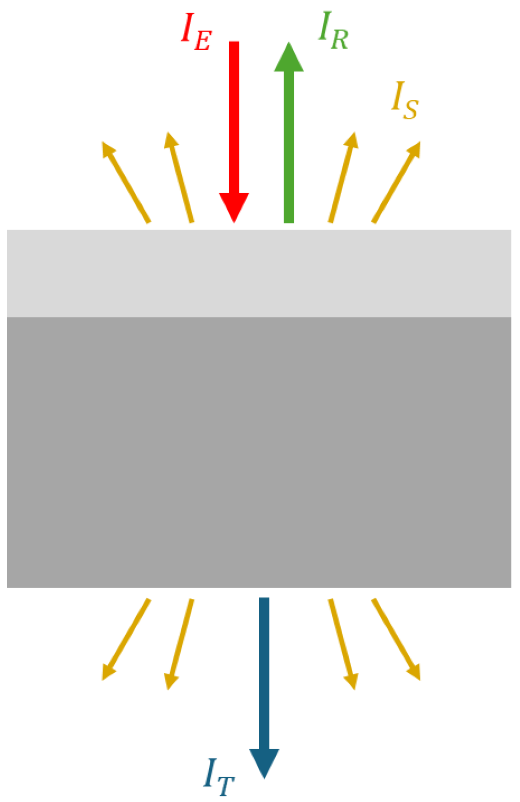
Figure 2.
Front- (left) and backside (right) illumination of a thin film on a substrate.
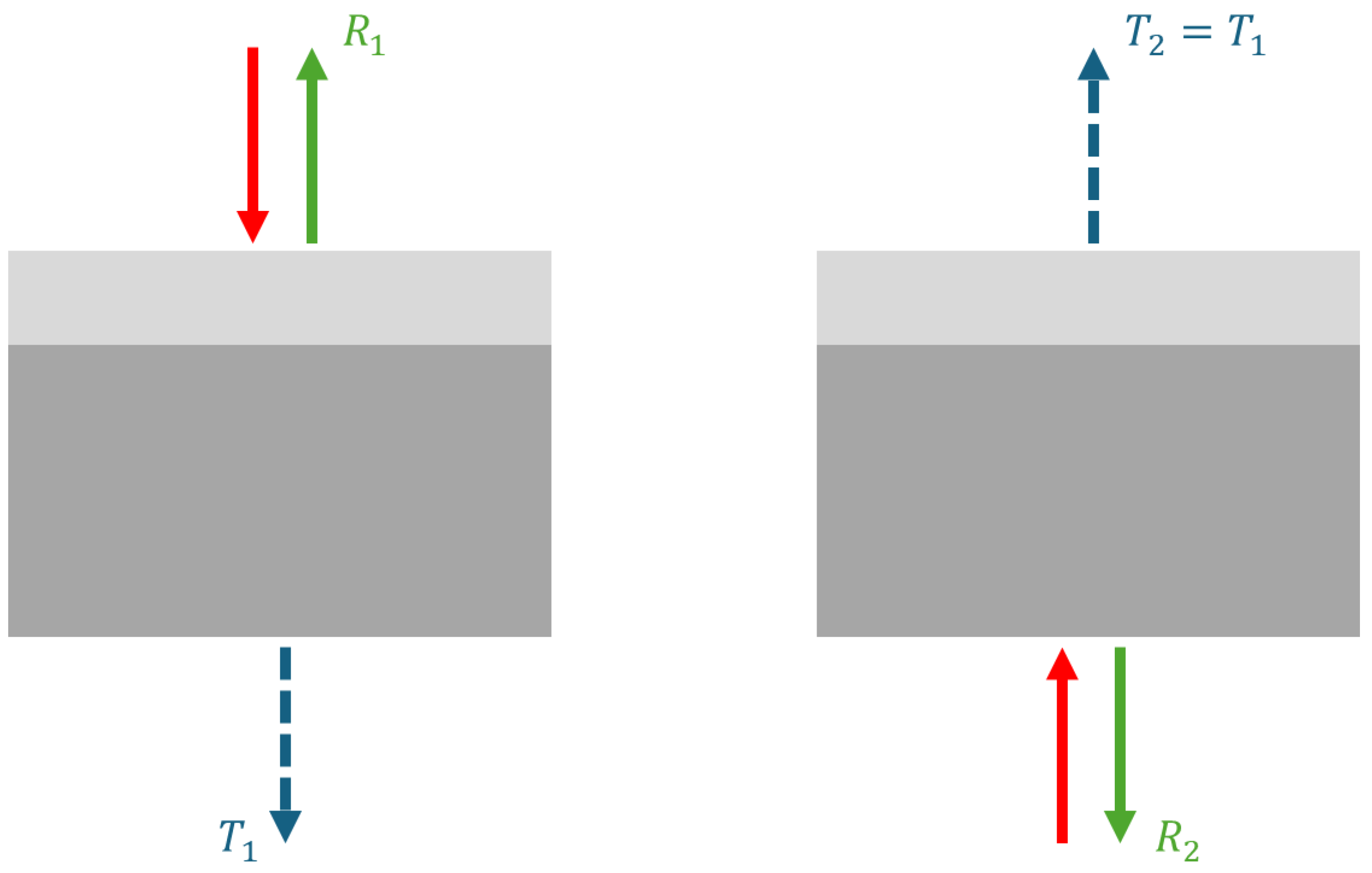
Figure 3.
Strongly absorbing sample.
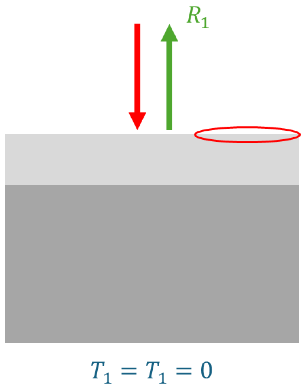
Figure 4.
Light transmission and reflection at an interface. Left: normal incidence, right: grazing incidence. Arrows indicate the direction of the electric field strength vector.
Figure 4.
Light transmission and reflection at an interface. Left: normal incidence, right: grazing incidence. Arrows indicate the direction of the electric field strength vector.
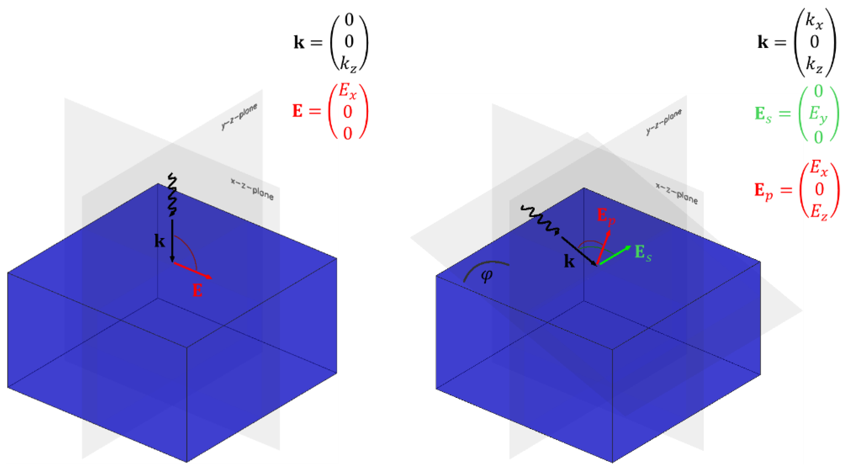
Figure 5.
Normal incidence reflectance of various metal surfaces on air. is the light wavelength in vacuum.
Figure 5.
Normal incidence reflectance of various metal surfaces on air. is the light wavelength in vacuum.
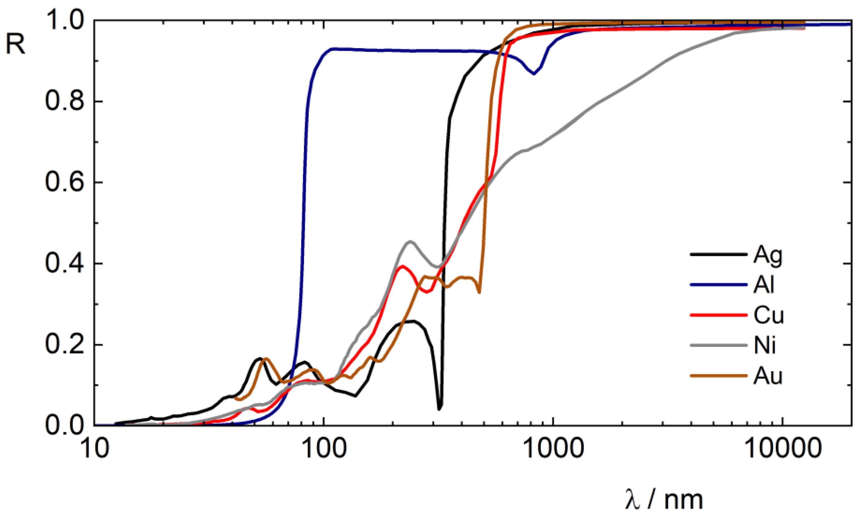
Figure 6.
Normal incidence reflectance of various dielectric or semiconductor surfaces on air.
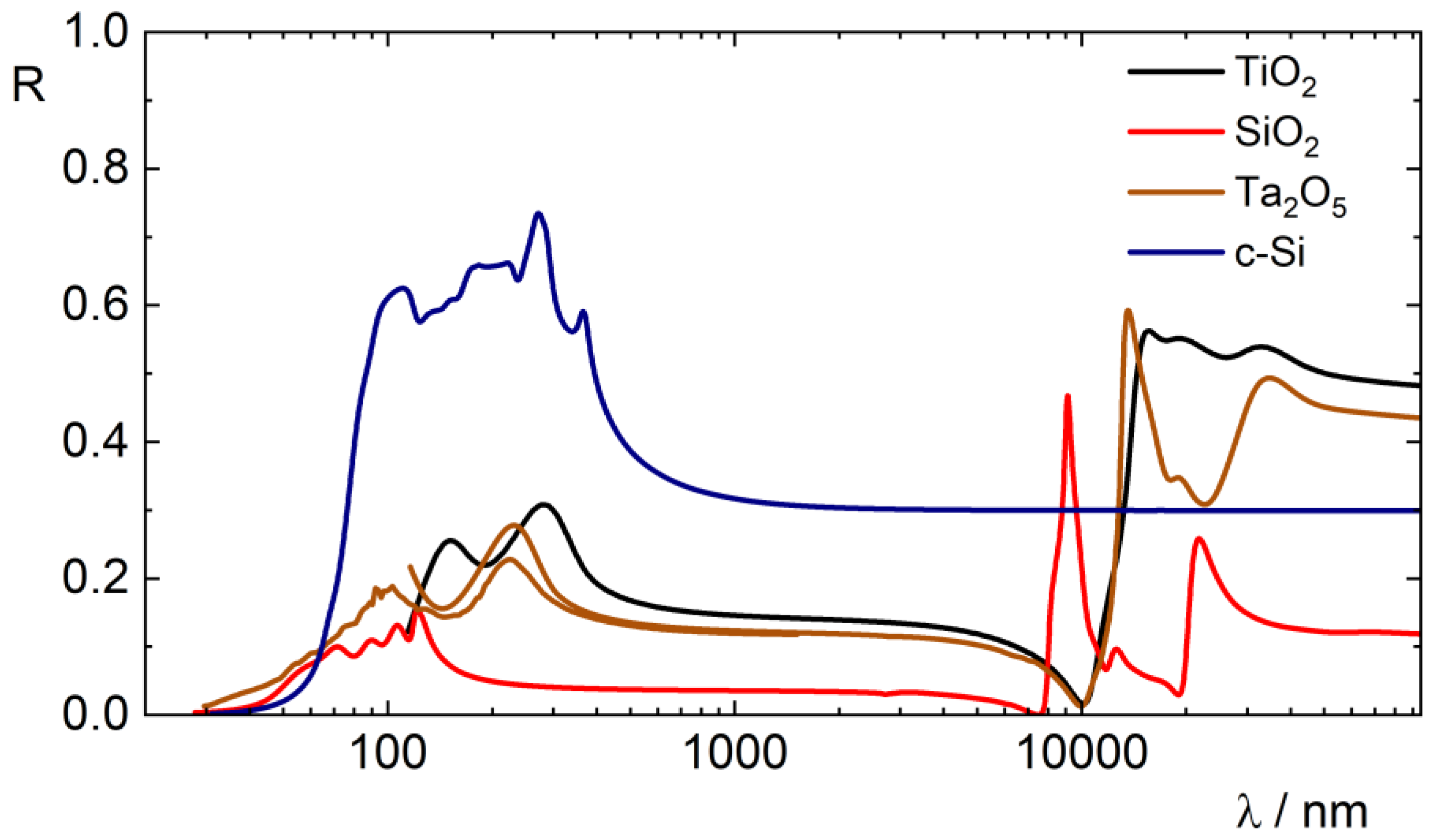
Figure 7.
Oscillating atomic dipole (left) modelled by a mass on a spring (right).
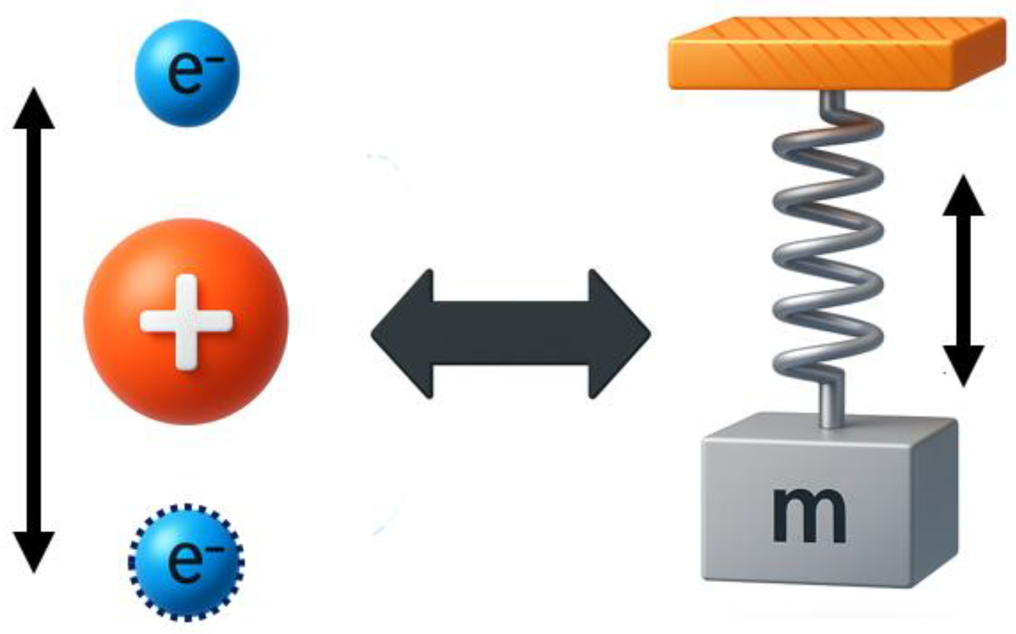
Figure 8.
Idealized normal incidence reflection spectra according to (20). Top: Drude metal; center: single oscillator model; bottom: two-oscillator model.
Figure 8.
Idealized normal incidence reflection spectra according to (20). Top: Drude metal; center: single oscillator model; bottom: two-oscillator model.
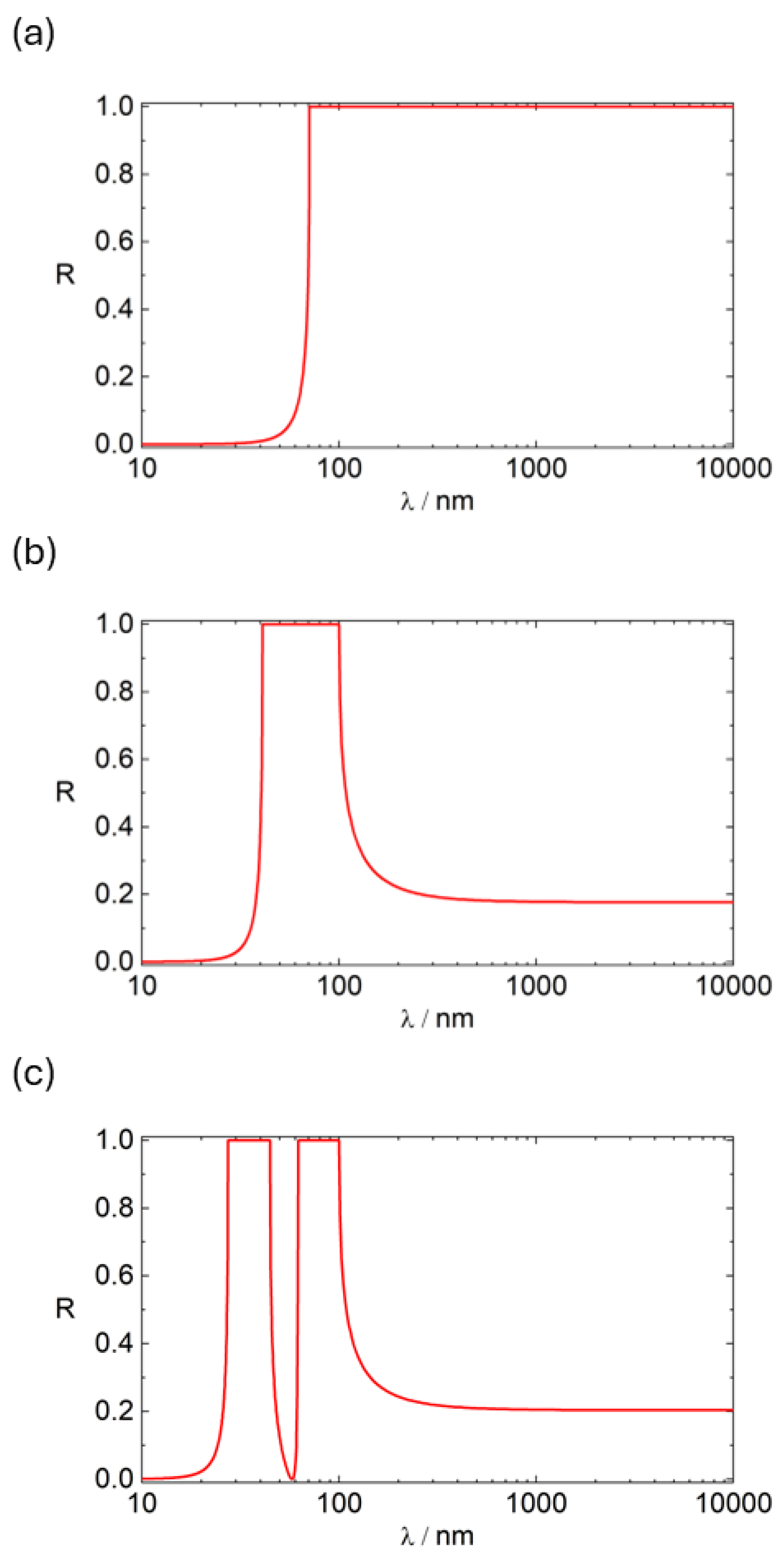
Figure 9.
Angular dependence of the reflectance of a metal surface.
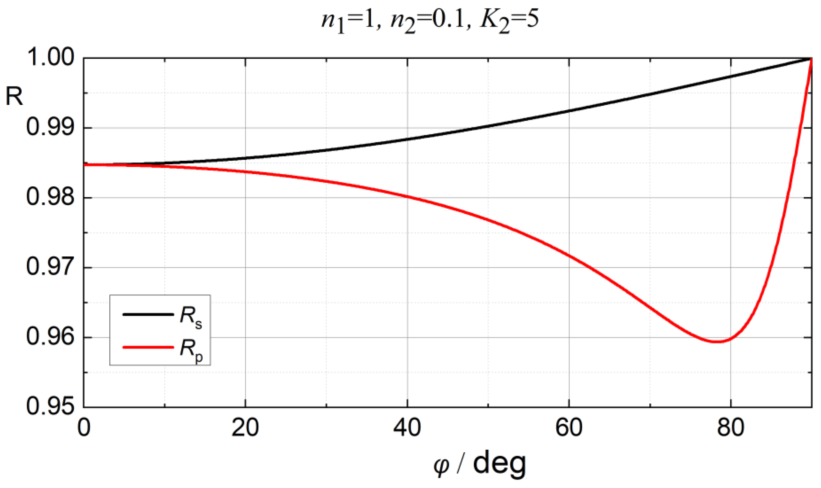
Figure 10.
Relative reflectance measurement with beam path for “auto zero” (a) and reflectance measurement (b). Intermediate spatial intensity distributions in the beam path are indicated by “L”.
Figure 10.
Relative reflectance measurement with beam path for “auto zero” (a) and reflectance measurement (b). Intermediate spatial intensity distributions in the beam path are indicated by “L”.
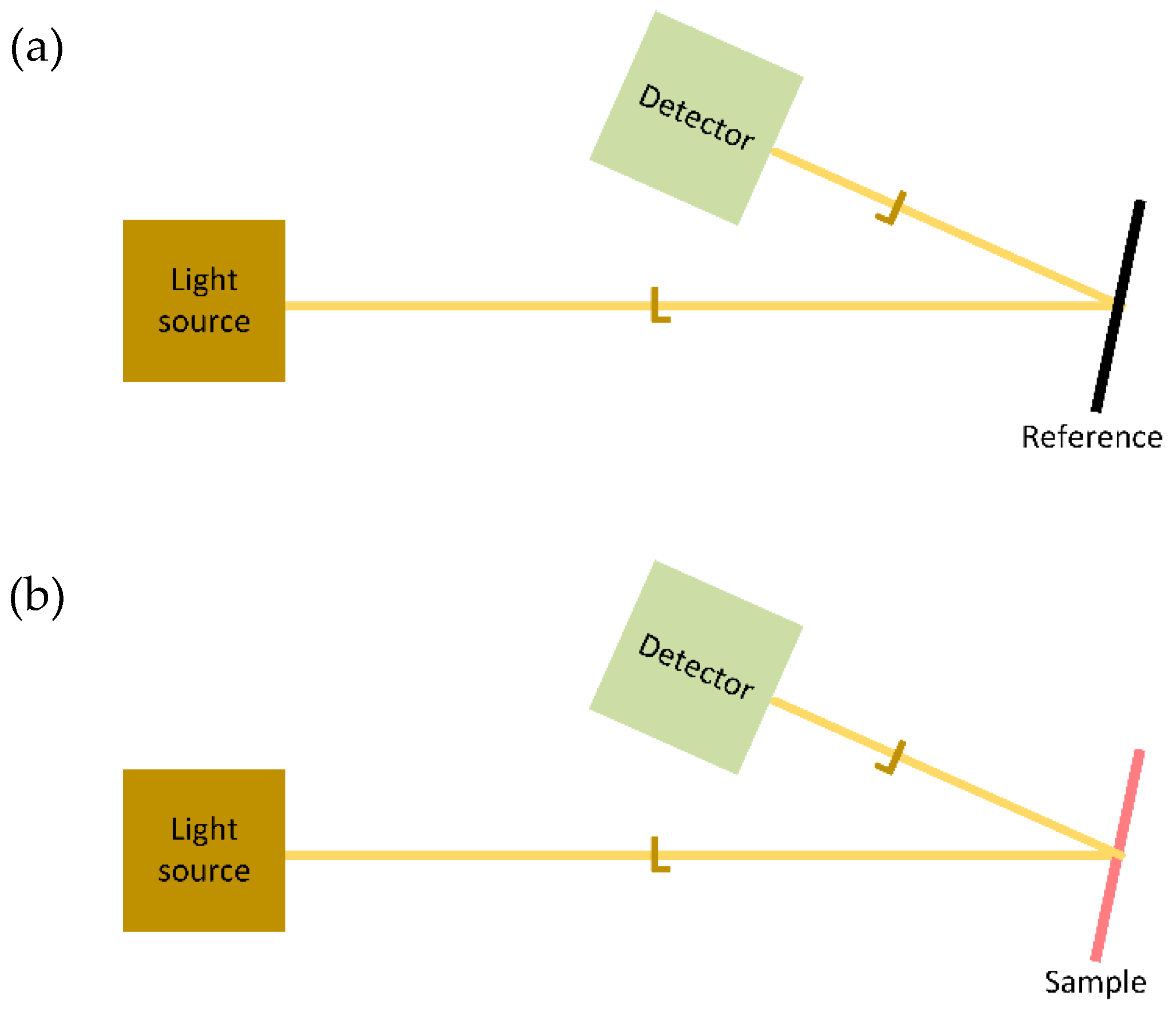
Figure 11.
Goniometer principle for absolute measurement with beam path for “auto zero” (a), transmittance (b) and reflectance measurement (c). Intermediate spatial intensity distributions in the beam path are indicated by “L”.
Figure 11.
Goniometer principle for absolute measurement with beam path for “auto zero” (a), transmittance (b) and reflectance measurement (c). Intermediate spatial intensity distributions in the beam path are indicated by “L”.
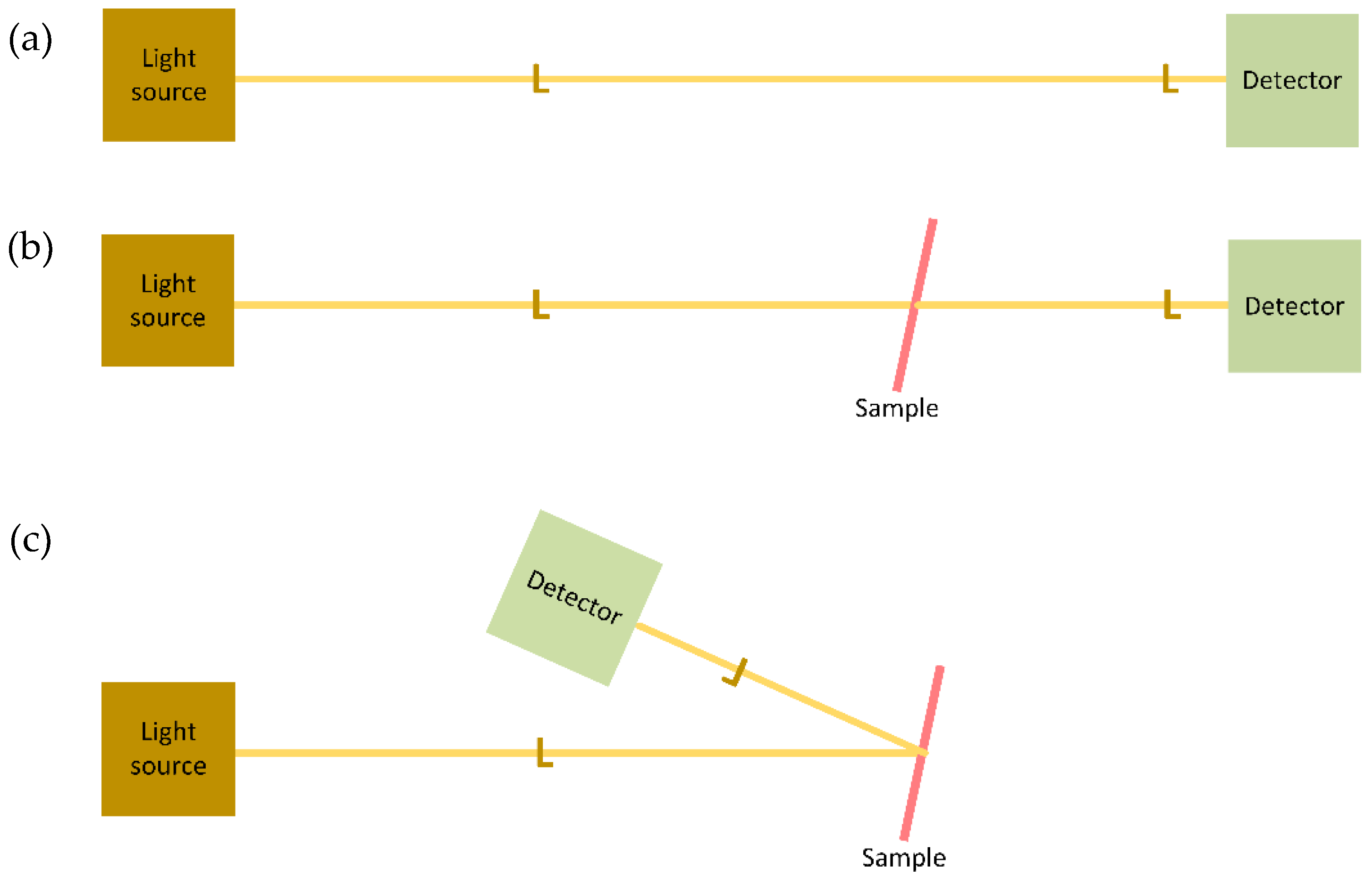
Figure 12.
VN-principle (named accordingly to the beam propagation shape “V” in transmittance and “N” in reflectance) for absolute measurement with beam path for “auto zero” (a), transmittance (b) and reflectance measurement (c). Intermediate spatial intensity distributions in the beam path are indicated by “L”.
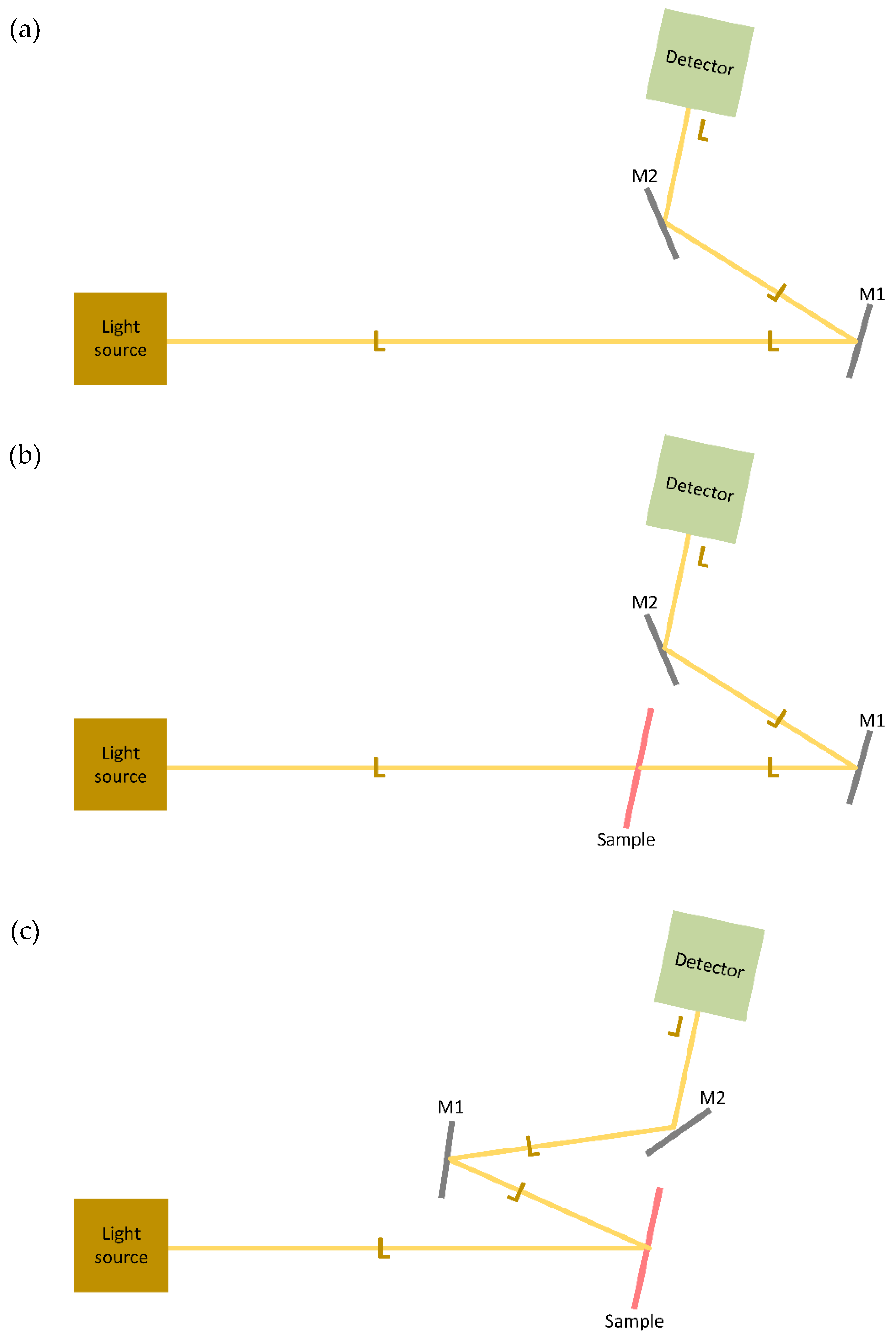
Figure 13.
VW-principle (named accordingly to the beam propagation shape “V” in transmittance and “W” in reflectance) for absolute measurement with beam path for “auto zero” (a), transmittance (b) and reflectance measurement (c). Intermediate spatial intensity distributions in the beam path are indicated by “L”.
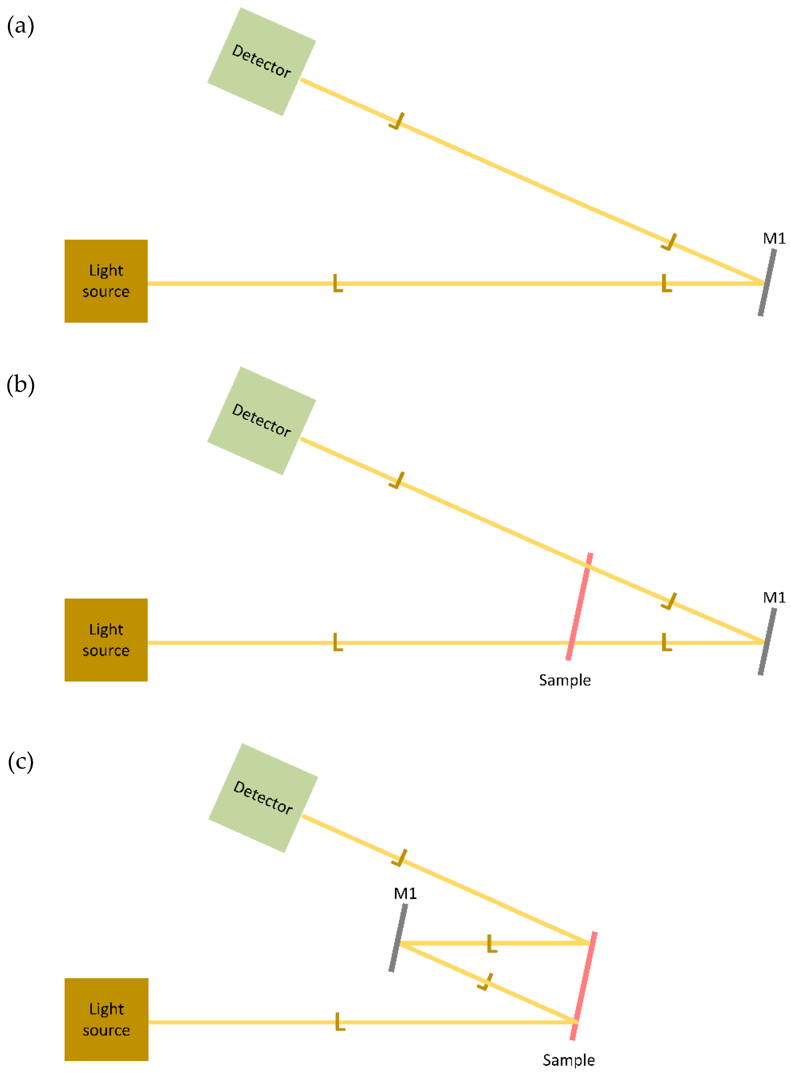
Figure 14.
IV-principle (named accordingly to the beam propagation shape “I” in transmittance and “V” in reflectance) for absolute measurement with beam path for “auto zero” (a), transmittance (b) and reflectance measurement (c). Intermediate spatial intensity distributions in the beam path are indicated by “L”.
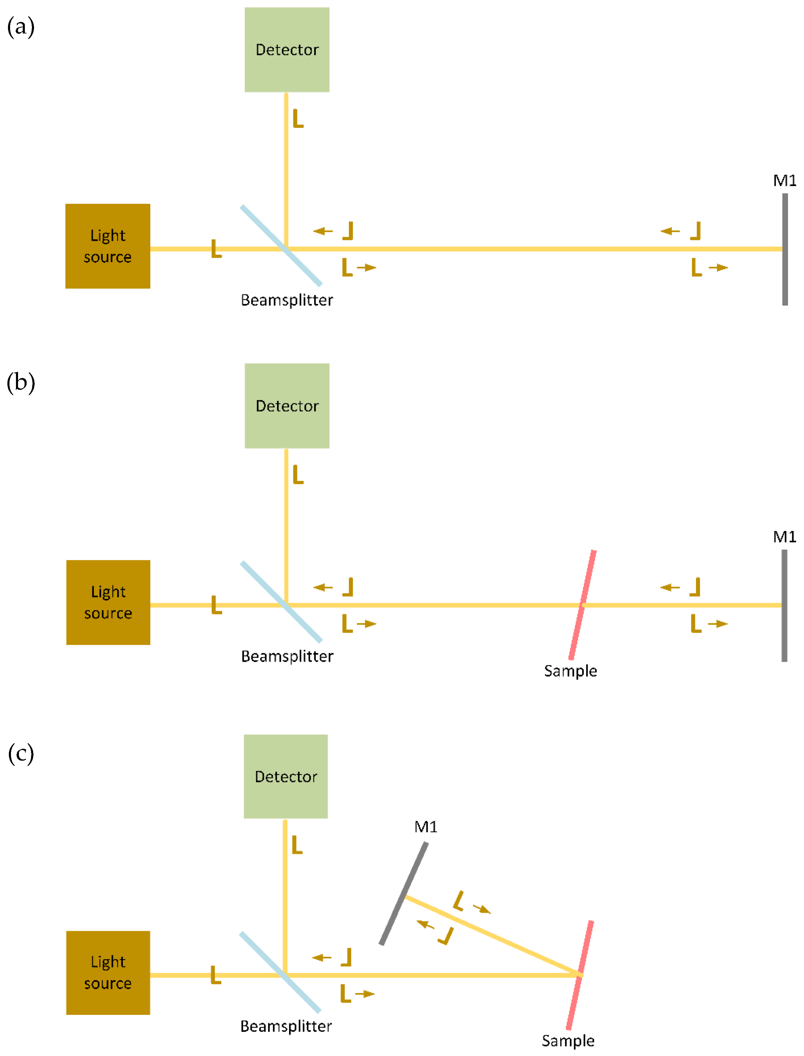
Figure 15.
Total reflection (solid lines) and attenuated total reflection (dashed lines) at the interface between two media with , , and .
Figure 15.
Total reflection (solid lines) and attenuated total reflection (dashed lines) at the interface between two media with , , and .
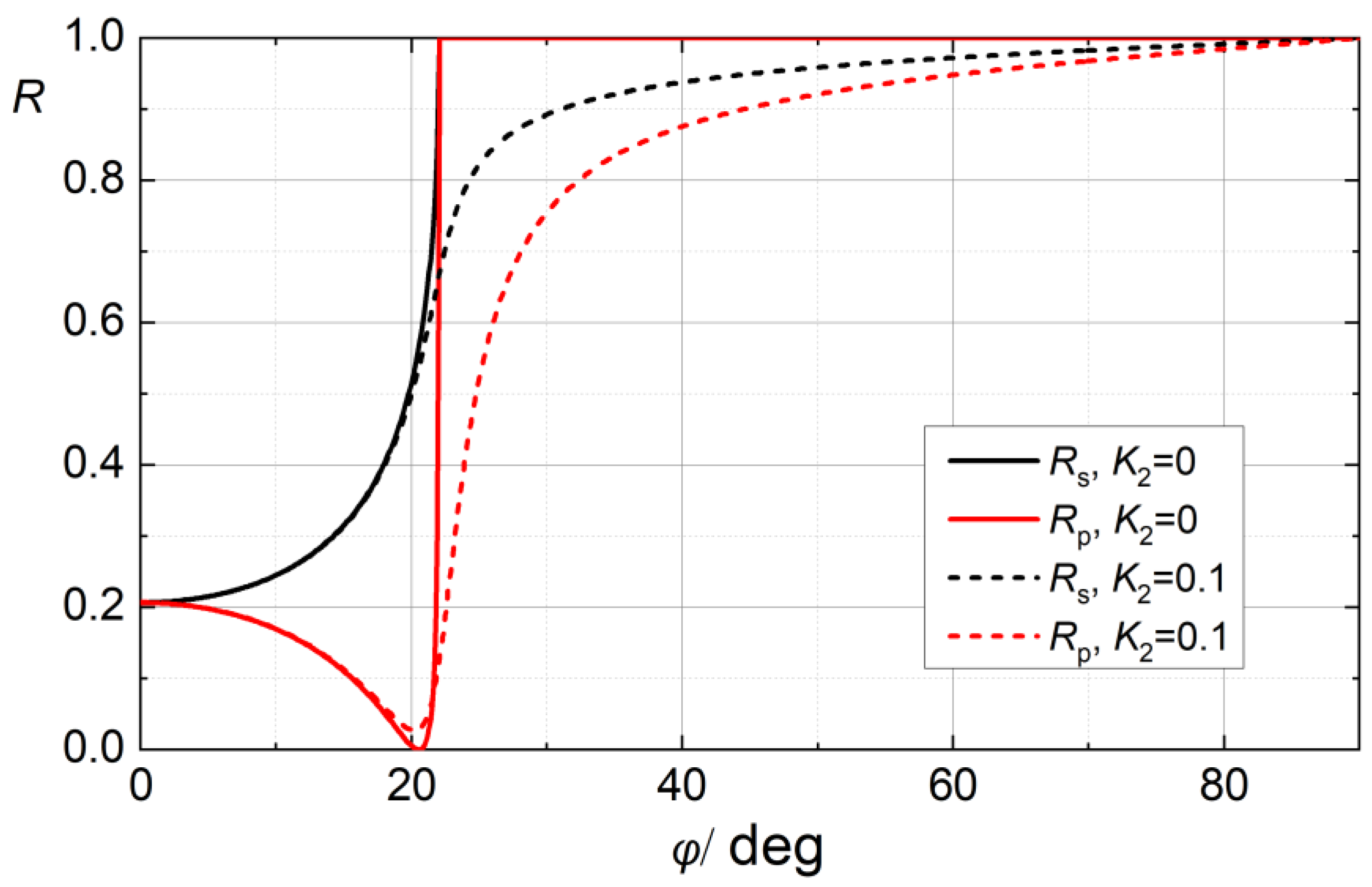
Figure 16.
Film system (thickness , material b) for reflectance at oblique incidence (angle ) with different media at frontside (medium a) and backside (medium c).
Figure 16.
Film system (thickness , material b) for reflectance at oblique incidence (angle ) with different media at frontside (medium a) and backside (medium c).
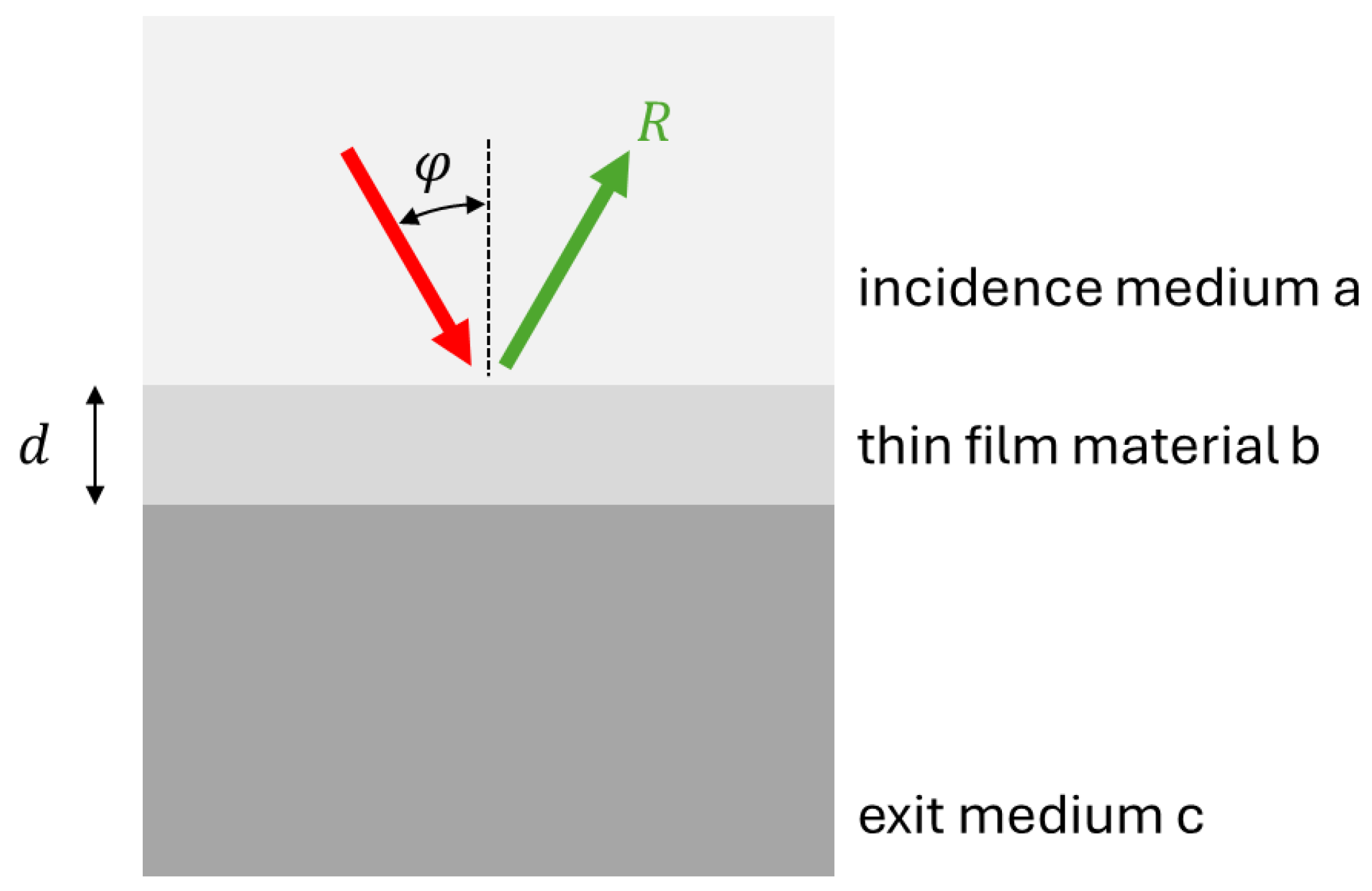
Figure 17.
Angular reflectance scan of a 43.8nm thick silver film on glass, λ=632.8nm, illumination from glass side. Triangles denote experimental data, solid lines calculations according to (43).
Figure 17.
Angular reflectance scan of a 43.8nm thick silver film on glass, λ=632.8nm, illumination from glass side. Triangles denote experimental data, solid lines calculations according to (43).
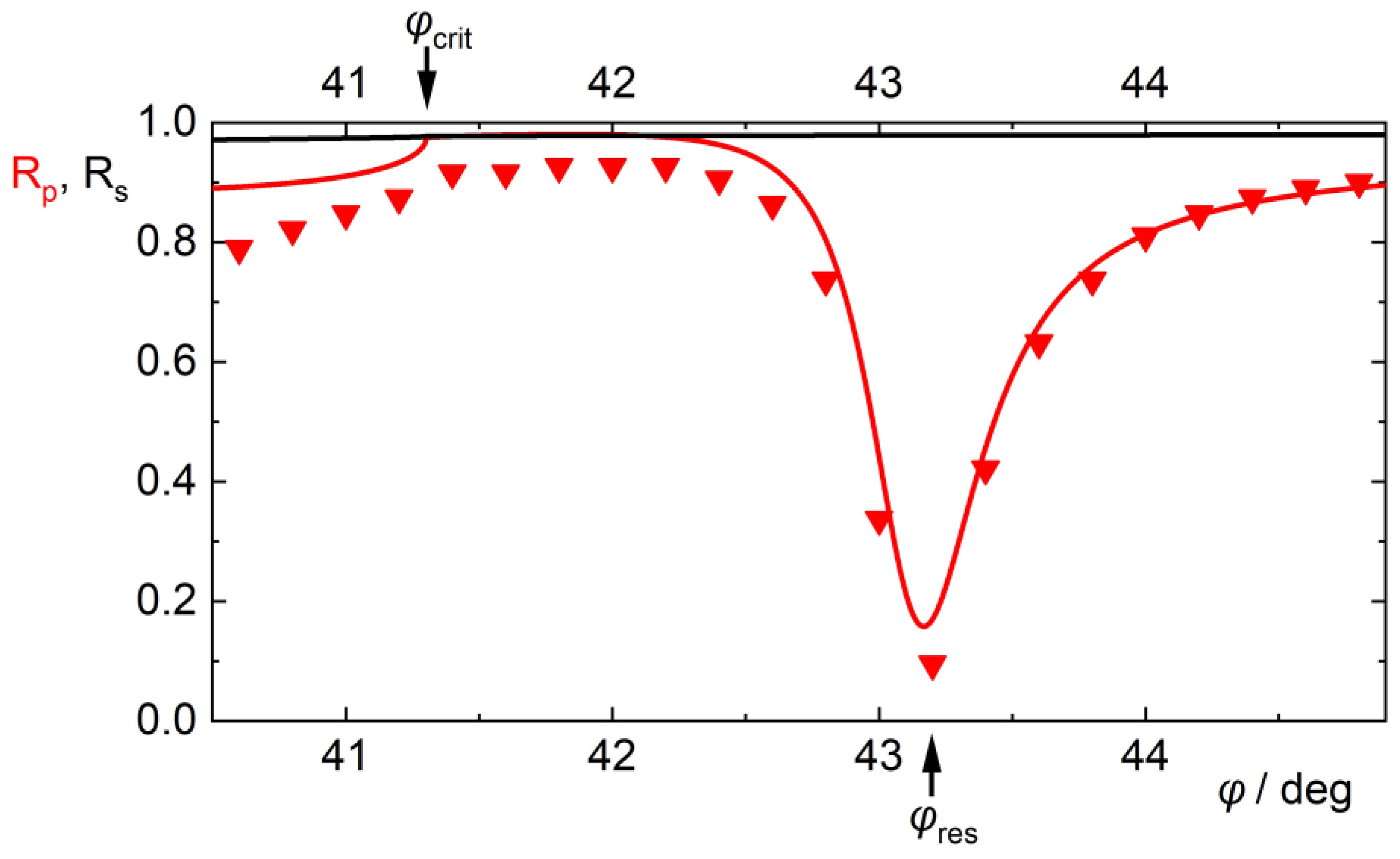
Figure 18.
Loss function (red), refractive index (blue), extinction coefficient (green) and imaginary part of the dielectric function (black).
Figure 18.
Loss function (red), refractive index (blue), extinction coefficient (green) and imaginary part of the dielectric function (black).
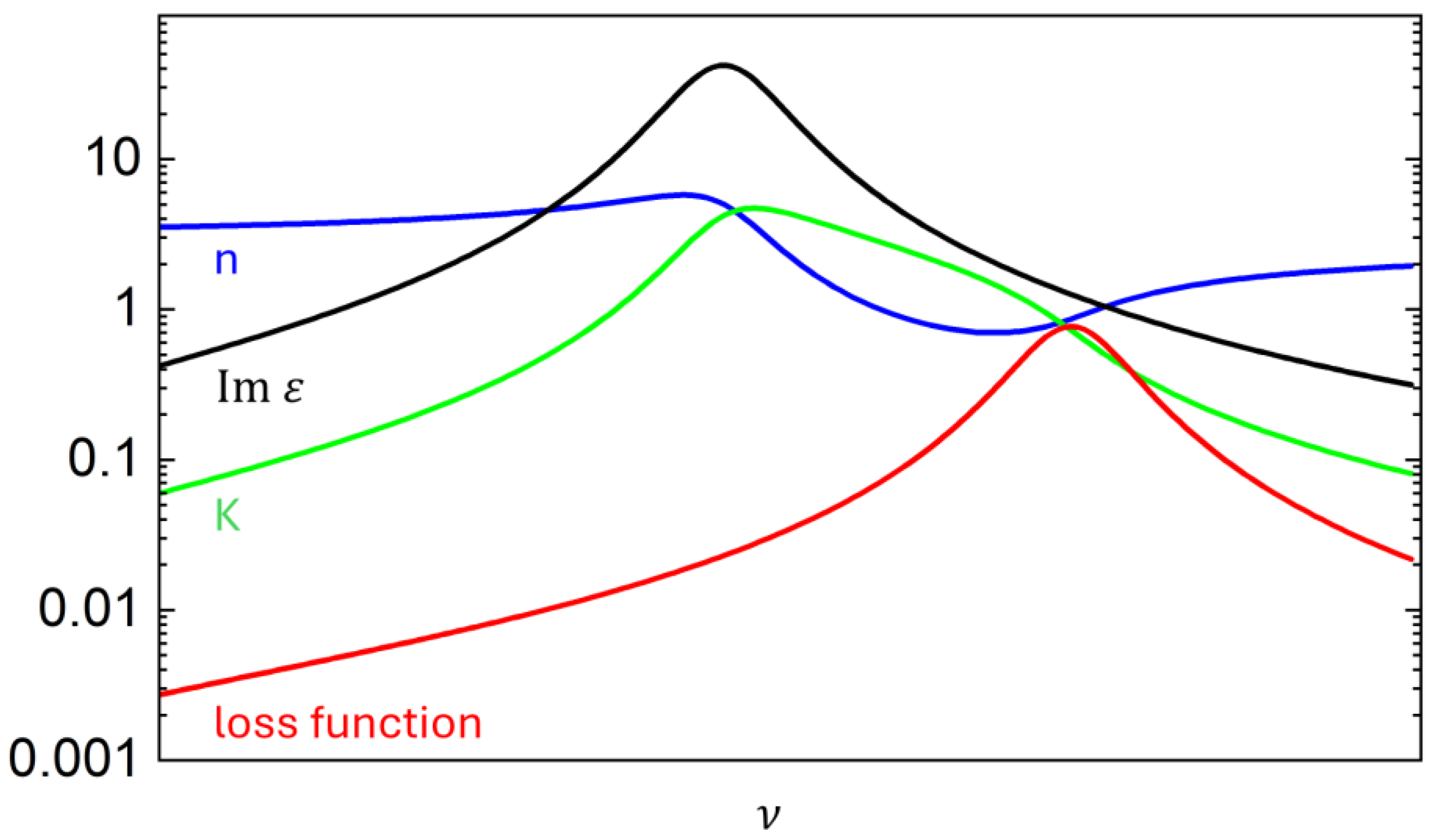
Figure 19.
Measured (circle) and modeled reflectance (solid line) of a ~105nm thick ITO layer on a silicon substrate at near normal incidence (a) and at 45° for s-polarization (b) and p-polarization (c); in (d): loss function (black solid line), imaginary part of dielectric function (dashed black line), refractive index (dotted blue line) and extinction coefficient (dotted green line).
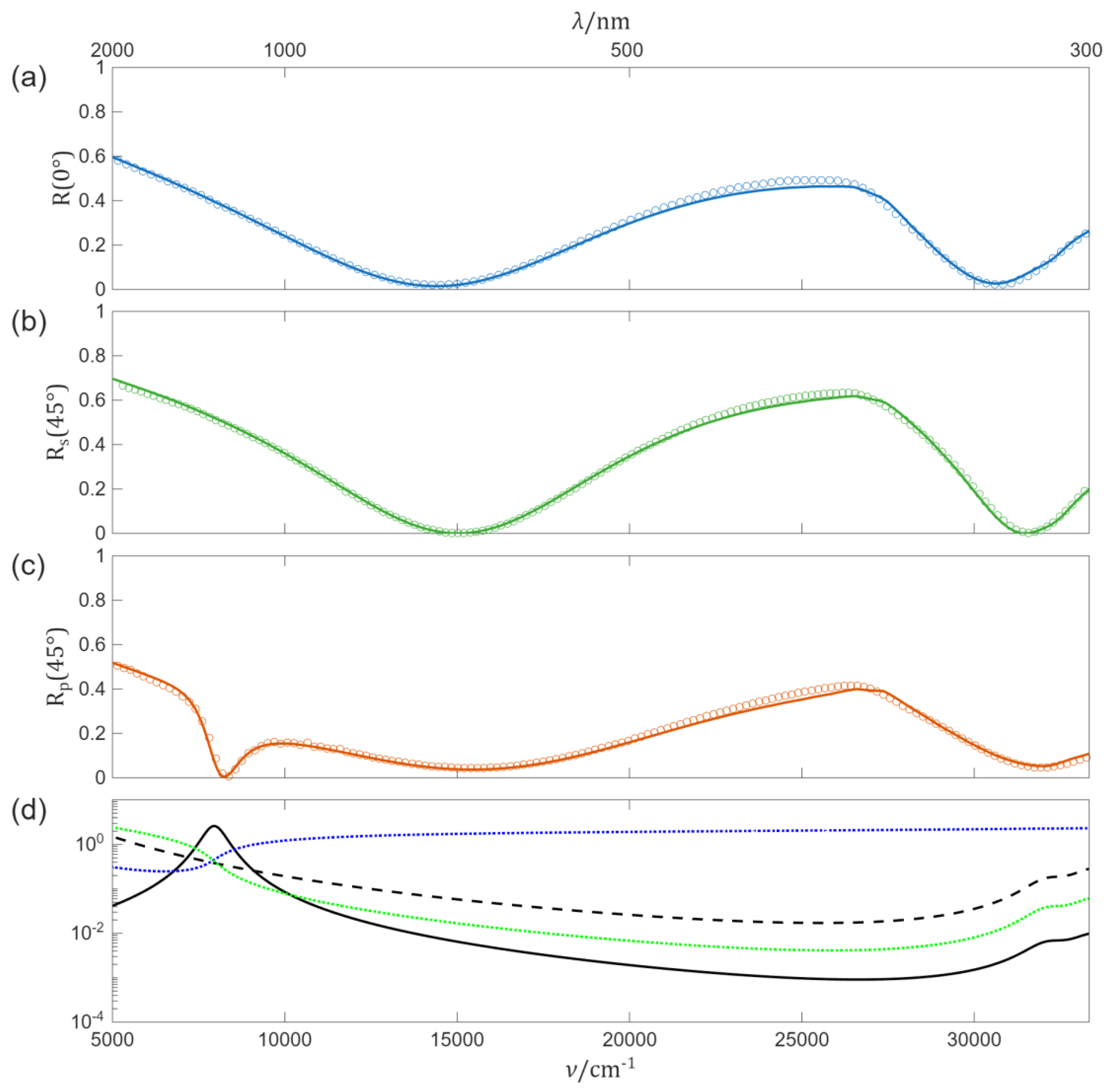

Table 1.
Common sequence of measurements and corresponding quantities.
| Step | Quantity | |||
| Sample beam | Reference beam | |||
| 1 | „Auto zero” | „100%“ | ||
| „0%“ | ||||
| 2 | Measurement | Sample | ||
Disclaimer/Publisher’s Note: The statements, opinions and data contained in all publications are solely those of the individual author(s) and contributor(s) and not of MDPI and/or the editor(s). MDPI and/or the editor(s) disclaim responsibility for any injury to people or property resulting from any ideas, methods, instructions or products referred to in the content. |
© 2025 by the authors. Licensee MDPI, Basel, Switzerland. This article is an open access article distributed under the terms and conditions of the Creative Commons Attribution (CC BY) license (http://creativecommons.org/licenses/by/4.0/).
Copyright: This open access article is published under a Creative Commons CC BY 4.0 license, which permit the free download, distribution, and reuse, provided that the author and preprint are cited in any reuse.


