
Submitted:
04 October 2025
Posted:
06 October 2025
You are already at the latest version
Abstract
The m-lines spectroscopy is a precise, non-destructive and contactless method, and one of its main applications is the determination of the geometric-optical parameters of a thin film deposited over a substrate, namely the refractive index and the thickness of the film under analysis. The method has been first described in the seminal work of Tien et al. [1] more than half a century ago and, since then, it has been reported in the literature that at least two modal indexes of the same polarization are required to unequivocally determine a given film’s refractive index and thickness. This constraint imposes a limit in the waveguide’s width, for it leaves out the possibility of determining the geometric-optical parameters of all films where only single mode propagation is feasible. In this work, we developed a strategy that, not only extends the width range calculation of the method down to single mode operation, but also the results’ analysis led us to conclude that by solely using the fundamental modes in the calculation, the method’s precision shall increase and the determined parameters should be closer to the physical reality of the film.
Keywords:
metrology
; m-lines spectroscopy
; refractive index
; thickness
; thin films
1. Introduction
M-lines spectroscopy is a non-destructive, contactless and highly accurate technique to optically characterize dielectric thin films. Its main functionality is to determine with high precision two fundamental parameters of a given thin layer of material deposited over a substrate: - The refractive index and thickness of the deposited film. This method has found applications in industry and academia, with recent increasing adoption by the former, especially where rigorous and precise characterization of dielectric films is a requirement. Follows examples of applications in industry:
-
Photonic Integrated Circuit manufacturing
- o
- Stakeholders: - Silicon photonics, optical sensors and telecommunications industries;
- o
- Industrial motivation: - Enables minimal tolerances over optical and dimensional parameters, thus improving overall coupling efficiency;
-
Coatings quality control
- o
- Stakeholders: - Laser components, high precision optics and photolithography;
- o
- Industrial motivation: - Refractive index and thickness validation of anti-reflection and highly protective coatings, and dielectric mirrors;
-
Microelectronics and semiconductors manufacturing
- o
- Stakeholders: - Micro-electro-mechanical systems, sensors and optoelectronics industries;
- o
- Industrial motivation: - Allows non-destructive analysis of dielectric layers deposited over semiconductor substrates and contactless inspection of layer parameters during or after deposition;
-
Functional glass manufacturing
- o
- Stakeholders: - Construction, auto and ultra-violet to infrared protection industries;
- o
- Industrial motivation: - non-destructive characterization of solar protective, electrically conductive, hydrophobic, anti-flare and multilayer films on dielectric substrate.
Developments of the m-lines spectroscopy method, as originally established by seminal work of Tien et al. in 1969 [1], have also taken place through academic research in more recent years. Approaches considering the application of numerical methods to include multilayer heterostructures, multiwavelength and new methods for data analysis, have also been proposed by Schneider et al. [2] where it is claimed the development of an equation for the simultaneous extraction of the refractive index and thickness of a three layer system, and Wu et al. [3] with a multiwavelength m-lines spectroscopy system with claimed advantages for the identification of refractive index profiles and dispersion.
This method bases its functionality on the excitation of the allowed propagation modes in a thin film. To achieve this, the modes propagating in the thin film couple into the incoming electromagnetic (EM) radiation through a coupling prism. Each of the allowed modes in the thin film couples into the EM radiation in the prism at a specific incoming angle, which corresponds to an interference dip in the reflection intensity graph produced by a monitoring photodetector. The incident angles on the prism’s edge, at which propagating modes are excited, refract towards the base and then reflected. Once these angles are known, it is possible to obtain the angles incident at the base of the prism through Snell’s law, and the modal index () of the excited mode is given by [4]:
where is the prism’s refractive index. The relation between the modal index of the propagating mode and its wavenumber () is:
where is the free space wavenumber. Figure 1 presents a diagram depicting the conservation of energy over the wavenumbers of the evanescent and propagating waves and the working principle of the method.
The method bases its functionality in the Frustrated Total Internal Reflection (FTIR) principle [5], which consists of the evanescent coupling of a given mode propagating in the thin film into the wave totally reflected at the prism’s base. Being an evanescent wave, the excitation of a given propagating mode requires close proximity between the thin film and the prism’s base. To achieve this, we use a pressure gauge to slightly deform the sample at the point of application of the force, hence diminishing the existing air gap between the prism’s base and the thin film, and enable evanescent mode coupling. Furthermore, the resonant angles incident at the prism’s edge (the ones measured) and the modal index of the excited modes are related by equation:
where and are the refractive index, and the internal angle formed between the base and the edge of the prism, respectively, is the refractive index of the air gap and the incident angles at the prism’s edge that excite propagating modes in the thin film.
Once we identify coupling features in the reflectance spectrum, the synchronous angles can be calculated using Snell’s law, for the corresponding incident angles at the prism interface - associated with each guided mode resonance - are now precisely known. This information, together with the knowledge of the modal indexes of the propagating modes in the thin film, allows determining the refractive index of the thin film layer by solving the following transcendental modes equation:
where is the wavenumber dependent effective width of the thin film (including the wave’s penetration in both substrate, , and cladding, , due to the Goos-Hänchen effect [6]) and is the actual width of the layer. Figure 2 depicts a diagram of the phase evolution of the propagating mode as it progresses in the thin film.
By examining Figure 3, the terms on the left hand side of Equation (4) can be further represented by the following expressions, where is the vacuum wavenumber, and and are the refractive index and the wavenumber of the thin film, respectively:
For perpendicular (free space propagation) [1] and Transverse Electric (TE - assuming propagation along the X-axis and non-vanishing , and field components in the thin film) polarization, we may write:
For parallel (free space propagation) [1] and Transverse Magnetic (TM - assuming propagation along the X-axis and non-vanishing , and field components in the thin film) polarization, the wave’s penetration either in the substrate and in the cladding (air), may be written as:
We have now all required to express Equation (4) with known quantities with the exception of the unknown (thin film refractive index) and (thin film width) variables. After replacing the terms in Equation (4) by the corresponding expressions in Equations (5)–(11) and algebraic simplification, we obtain the following equations according to polarization:
These are two variables transcendental equations and not easy to solve through analytical methods. The usual way of solving these equations is by eliminating the width () variable by operating a division between two equations, each resulting from the expression obtained when considering two different modes of the same polarization. For instance, when considering TE polarization and the modal indexes of the fundamental () and first () propagation modes:
Similarly, when considering TM polarization and the modal indexes of the fundamental () and first () propagation modes:
Hence, it has been claimed throughout the years [3,7,8,9,10] this method requires at least the knowledge of two modal indexes of the same polarization to unequivocally determine its refractive index and thickness, which imposes dimensional constraints in the waveguide’s parameters calculation. To illustrate this, we assume a usual asymmetric thin film deposited over an optical glass substrate with 1.8 and 1.528 refractive indexes, respectively, and plot the allowed modes as a function of the thickness of the waveguide, for a given excitation wavelength. We used FemSIM from RSoft [11] to calculate the excited modes and as can be observed in Figure 4, the first modes start being excited when the width of the thin film is above 400 nm, more precisely at ~400 and ~450 nm for TE and TM modes, respectively. Thus, since m-lines spectroscopy requires at least two modes of the same polarization to solve Equation (15), this technique is limited to ~400 nm thick thin films for reliable measurement, considering the asymmetric thin film configuration depicted in Figure 4.
In this work, we use the m-lines spectroscopy method to determine the refractive index and thickness of asymmetric thin films, by solely utilizing the fundamental mode of each polarization (TE0 and TM0) to compute the intended parameters of the deposited film. This way, we avoid the thickness constraint imposed by the two modes of the same polarization requirement for reliable computation, and we are now able to calculate these parameters for much thinner films, only limited in thickness by the degree of asymmetry of the thin film. Namely, and returning to the thin film configuration depicted in Figure 4, calculation is still limited by the refractive index of the substrate, only this once by the TM fundamental mode instead of the first mode (W > ~150 nm).
In the next section, 2. Materials and Methods, we present the implemented optical setup with a thorough description of its constituents. Follows section 3. Results, where we report our findings and describe all steps and actions performed in this research work. Finally in section 4. Discussion, we present a critically aware assessment of this research work and its findings, discuss our conclusions and define future work directions.
2. Materials and Methods
We developed an optical setup to obtain the optical-geometric parameters of a Si2C2N6 film deposited over an optical glass (AF-45) substrate. The characterization consisted of determining the refractive index and thickness through the m-lines spectroscopy method. We accomplished this by implementing an optical setup which monitors the photodiode current as a function of the incident/reflected angle. Figure 5 presents a photograph of the implemented optical setup:
As depicted in Figure 5, the optical setup consists of a 655 nm laser diode (top right in photograph), follows a polarizer (Thorlabs LPVIS100) enabling the selection of parallel or perpendicular polarizations, hence the selective excitation of transverse magnetic or transverse electric mode resonances, the rotary stage is an angular motor/actuator (Thorlabs PRM1-Z8) and the motor driver (Thorlabs KDC101) controls the rotary stage. Mounted on two posts attached to the rotary stage there is a 5-axis stage (Thorlabs PY005), allowing for X, Y, Z, pitch and yaw adjustments, onto which the prism holder is secured. Attached to the prism holder there is a lever, where a weight might be placed to exert mechanical force to the backside of the sample’s substrate, thus controlling prism/film coupling through adjustment of the distance between the prim’s base and the Si2C2N6 film. We attach the photodetector to the prism holder and placed it right next to the prism’s edge where the reflected beam exits. We monitor the generated photocurrent in the photodetector with a multimeter (Rigol DM-3058). A computer controls the optical setup through USB and monitors the angular movement of the rotary stage, and the photocurrent generated by the beam reflected from the prism’s base.
3. Results
We started this research work with a sample consisting of an AF45 glass substrate [12], with the thin film deposited on the substrate through Plasma Enhanced Chemical Vapor Deposition. The fabrication conditions, deposition and characterization details of the selected silicon carbonitride sample (Si2C2N6) are described elsewhere [13]. We used this sample to test, verify and confirm the validity of our hypothesis: - The limit in the m-lines spectroscopy method is the thickness necessary to propagate the fundamental modes of both polarizations, Transverse Electric (TE0) and Transverse Magnetic (TM0).
Using the m-lines spectroscopy optical setup with the Si2C2N6 sample loaded on, we observed the reflectance versus incident angle as presented in Figure 6:
We obtained these results with an angular step of 0.05°, at the operating wavelength of 655 nm provided by an off-the-shelf laser diode and a polarizer placed in the optical beam path, between the laser diode and the prism. In both graphs of Figure 6, one is able to identify three dips corresponding, from right to left, to the interference of the returning laser beam when at normal incidence on the prism’s edge, which we use as our 45° reference, and to the modes which have been excited in the film. Depending on how the goniometer rotates anti- or clockwise, the measured angles may have to be subtracted from 90°; such happened in this case.
Equation (3) returns the modal indexes of the excited modes (), given the incident angles at the prism’s edge () and corresponding synchronous angles (). Since these are known quantities, we are now able to solve numerically Equation (4) and determine the refractive index and thickness of the film, as long as the refractive indexes of the substrate, air gap and prism are known. Before proceeding with calculations, let’s examine further dispersion Equation (4) considering the analysis initiated by Tien [14] and further pursued by other researchers [15,16]: - Simply put, Equation (4) is thought to be incomplete, for it does not consider the prism’s influence on a given propagating mode in the film.
In fact, by analysing the terms on the left hand side of Equation (4), one finds, from left to right, a term related to the width of the film () and the terms related to the field’s penetration in both substrate () and superstrate (). These terms are further algebraically simplified, resulting in Equations (14) and (15) for TE and TM modes, respectively, and the influence of the prism remains absent, not accounted for in these equations. The same is true even graphically in Figure 2 and Figure 3, where the presence of the prism has been coherently removed. As such, the solution found by Equations (14) and (15) should reflect the calculation of the film’s refractive index, when accounting for TE and TM modes with a semi-infinite air superstrate. Hence, the obtained modal indexes are real-valued propagation constants, corresponding to propagating modes confined in the film. Then, we derive the film’s thickness through the just calculated refractive index.
We investigated further the modal indexes of a given structure with the FemSIM mode solver, assuming 572 nm and 1.869004116 for the thickness and refractive index of the silicon carbonitride film, with two different structure configurations:
- -
- Semi-infinite substrate/thin film/semi-infinite airgap;
- -
- Semi-infinite substrate/thin film/airgap/semi-infinite prism.
Figure 7 shows the amplitude profiles and corresponding modal indexes of representative results obtained with the mode solver (propagation is along the Z-axis and film confinement along the X-axis in FemSIM, thus the electric field designations associated to TE/TM are opposite the convention used in Figure 2 and Figure 3), followed by Table 1 with the values returned by the mode solver of the excited modes in the film.
It is notorious the difference in the amplitude profiles between the modes calculated by the mode solver with semi-infinite air superstrate and with 100 nm airgap/semi-infinite prism. The modes of the latter show field leakage through the gap and into the prism. This is further confirmed by comparing the imaginary components of the modal indexes when the superstrate is semi-infinite air or airgap/semi-infinite prism. The former modes are essentially film confined modes, while the latter are leaky modes. Moreover, the real components of the modal indexes, when comparing the same mode order of each configuration, are not equal and impact the results returned by dispersion Equation (4) when calculating the refractive index and thickness of the film.
To fully model this system and account for the accumulated phase through the gap, we must replace in the classic dispersion equation the term related to the phase in the air gap (), by the one representing the effective phase of the prism/gap system ():
This may be achieved by looking at the system gap/prism as a transmission line, considering normalized admittances:
- , for TE polarization;
- , for TM polarization.
where , is the refractive index of either gap or the prism and is the free space wavenumber. As such, the input admittance seen by the film towards the prism is:
where superscript stands for polarization TE/TM, and subscripts , and , stand for superstrate, gap and prism, respectively. To recover the accumulated effective phase, we may use:
- , for TE polarization;
- , for TM polarization.
and obtain:
However, this strategy is air gap dependent, for variable incorporates the term and is the not known air gap thickness. Nevertheless, we have implemented and tested this solution, but the results obtained were slightly worse than the ones obtained when solving the classical dispersion Equation (4). As such, this strategy was abandoned, and we proceeded focusing our research on the analysis of the results obtained with Equation (4).
Next and using the angles experimentally obtained and presented in Figure 6, and dispersion Equation (4), the film’s calculated refractive index and thickness are presented in Table 2:
As may be observed in Table 2, there is a differential between the TE and TM calculated values, namely and for the refractive index and thickness, respectively.
We then evaluated the impact of angular resolution on the obtained results. To this end, we analyzed once again the silicon carbonitride film sample, only this time with a finer resolution of 0.01 degrees. Table 3 shows all the pertaining information, from the resonant angles to the calculated refractive indexes and thicknesses, in both TE and TM polarizations:
From Table 3 we notice a change in the differential between the TE and TM calculated values, being now and for the refractive index and thickness, respectively. The greater resolution assured a smaller difference in the TE and TM calculated thicknesses, although there’s a slight increase in the refractive index differential.
With previous thought in mind, we analyzed once more the silicon carbonitride sample with an even greater angular resolution, 0.001 degrees. This was the only occasion we performed an analysis at such a fine resolution, for when one knows nothing about the film’s thickness and refractive index, it is good practice to scan a wide range of angular positions (10 to 80 degrees). However, this is a lengthy process at an angular step of 0.001 degrees. The results obtained are presented in Table 4:
The difference between TE and TM values has decreased significantly, reaching now and . Moreover, there is an evident trend of a diminishing differential as the angular resolution of our goniometer increases and an inversion of the sign of the results, which suggests there should be a minimum where the derivative of each differential reaches zero. Plus, by following the behavior of the refractive index as the angular resolution increases, one notices that TE and TM are affected differently. The TM calculated refractive index presents greater variation, while TE values are more stable.
Another constraint affecting the concordance of TE and TM calculated refractive indexes, and which has been referred to in the literature [17], is the force applied to approximate the substrate to the prism and favor coupling. As the exerted force is increased, the coupling resonances are widened and shifted, hence care must be taken to avoid these issues.
Previous analysis is in line with the fact that there is only one refractive index of the film deposited on the glass substrate, despite the calculation process involving TE or TM dispersion related equations. As such, the actual film’s refractive index must be the one that is better approximated by the results obtained by both TE and TM calculations. With this in mind, we have executed once more the process of determining the refractive index and thickness of our film, only this time we used just the fundamental modes to solve the dispersion equations. By solely utilizing TE0 and TM0 to calculate the intended parameters of the deposited film, we are now able to calculate the refractive index and thickness of thinner films (W > ~150 nm). This may be concluded by inspecting the graph depicted in Figure 4, where the limit is now imposed by the intersection between the TM fundamental mode and the substrate line instead of, as previously, between the substrate line and the first TM mode.
Equation (19) has been used to calculate the optical-geometric parameters and Table 5 presents the results obtained:
As can be observed in Table 5, this calculation scheme produces a single value for the refractive index and the TE/TM thickness differential is the smallest one so far, . We believe these are the closest to physical refractive index and thickness values, since it presents the smallest differential, but also because the calculation relies on the TE and TM fundamental modes. Fundamental modes present the highest modal index of any propagating mode in a given film, which means their propagating path is the closest to the guide’s center, hence less prone to the influence of the prism’s medium proximity. We assured the least possible exerted force on the backside of this sample, thus previous assumption regarding our measurements being the closest possible to physical reality of the sample.
4. Discussion
We started this research work to evaluate the possibility of extending the measurement range of the m-lines spectroscopy method. To this end, we conducted a series of analyses of increasing resolution on a silicon carbonitride film deposited over a glass substrate. Each analysis considered finding the optical-geometric parameters of the film under test, namely the refractive index and thickness. To determine these parameters, we considered initially the calculation strategy that has been reported throughout the years in the literature, since the seminal work of Tien et al. [1]: - The method requires two modes of the same polarization to solve the transcendental equations.
By using transverse electric and magnetic Equations (14) and (15), we are able to obtain two pairs of parameters, one for each polarization, which we can compare. Ideally, since there is only one film, both calculations should present the same result for each parameter, but experimental results are hardly ideal. However, as we increased the angular resolution in the optical setup, we noticed a decreasing trend of the refractive index and thickness differentials when comparing parameters of both polarizations. The obtained differentials for an angular resolution of 0.001° were and . Next, with the same data as before and using the fundamental modes of each polarization, we determined a thickness differential of . Not only is this the lowest differential obtained, but by determining the optical-geometric parameters with the fundamental modes, we are able to extend the range of application of the m-lines spectroscopy method to thinner films, as it is the intent of this research work.
Further work will consider the physical verification of the results obtained. To this end, we intend to fabricate a sample that will provide access to a high precision measuring system (e. g. atomic force microscopy) to determine the film’s thickness, while still allowing probing by the m-lines spectroscopy method, and confirm whether or not this strategy is valid.
Author Contributions
Conceptualization, Paulo Lourenço; methodology, Paulo Lourenço; software, Paulo Lourenço; validation, Alessandro Fantoni; writing—original draft preparation, Paulo Lourenço; writing—review and editing, Alessandro Fantoni; funding acquisition, Paulo Lourenço and Alessandro Fantoni. All authors have read and agreed to the published version of the manuscript.
Funding
This research was supported by Portuguese national funds provided by the Portuguese Fundação para a Ciência e a Tecnologia (FCT) program, Center of Technology and Systems (CTS) UIDB/00066/2020/UIDP/00066/2020, and by IPL projects IPL/IDI&CA2024/OPAPIC2D_ISEL e IPL/IDI&CA2024/REFINDEX_ISEL.
Data Availability Statement
No new data were created or analysed in this study. Data sharing is not applicable to this article.
Conflicts of Interest
The authors declare no conflicts of interest.
References
- Tien, P.K.; Ulrich, R.; Martin, R.J. Modes of propagating light waves in thin deposited semiconductor films. Applied Physics Letters 1969, 14, 291–294. [Google Scholar] [CrossRef]
- Schneider, T.; Leduc, D.; Cardin, J.; Lupi, C.; Gundel, H. Optical Characterisation of a Three Layer Waveguide Structure by m-Lines Spectroscopy. Ferroelectrics 2007, 352, 50–60. [Google Scholar] [CrossRef]
- Wu, Y.-C.; Villanueva-Ibañez, M.; Le Luyer, C.; Shen, J.; Mugnier, J. Application of multi-wavelength M-lines spectroscopy for optical analysis of sol-gel prepared waveguide thin films. In A. Rosental,ed., (2005), pp. 59461E-59461E–12. [CrossRef]
- Tien, P.K.; Ulrich, R. Theory of Prism–Film Coupler and Thin-Film Light Guides. Journal of the Optical Society of America 1970, 60, 1325–1337. [Google Scholar] [CrossRef]
- Hecht, E. Optics 5th Edition (2016).
- Goos, F.; Hänchen, H. Ein neuer und fundamentaler Versuch zur Totalreflexion. Annalen der Physik 1947, 436, 333–346. [Google Scholar] [CrossRef]
- Ulrich, R.; Torge, R. Measurement of Thin Film Parameters with a Prism Coupler. Applied Optics 1973, 12, 2901. [Google Scholar] [CrossRef] [PubMed]
- Ding, T.-N.; Garmire, E. Measuring refractive index and thickness of thin films: a new technique. Applied Optics 1983, 22, 3177. [Google Scholar] [CrossRef] [PubMed]
- Cardin, J.; Leduc, D.; Schneider, T.; Lupi, C.; Averty, D.; Gundel, H.W. Optical characterization of PZT thin films for waveguide applications. Journal of the European Ceramic Society 2005, 25, 2913–2916. [Google Scholar] [CrossRef]
- Cardin, J.; Leduc, J. Determination of refractive index, thickness, and the optical losses of thin films from prism-film coupling measurements. Applied Optics 2008, 47, 894–900. [Google Scholar] [CrossRef] [PubMed]
- FemSIM, FemSIM - Synopsys. (n.d.). https://www.synopsys.com/photonic-solutions/rsoft-photonicdevice-tools/passive-device-femsim.html (accessed September 28, 2025).
- refractiveindex.info; Refractive index database. (n.d.). https://refractiveindex.info/ (accessed September, 2025).
- Lavareda, G.; Vygranenko, Y.; Amaral, A.; de Carvalho, C.N.; Barradas, N.P.; Alves, E.; Brogueira, P. Dependence of optical properties on composition of silicon carbonitride thin films deposited at low temperature by PECVD. Journal of Non-Crystalline Solids 2021, 551, 120434. [Google Scholar] [CrossRef]
- Tien, P.K. Light Waves in Thin Films and Integrated Optics. Applied Optics 1971, 10, 2395. [Google Scholar] [CrossRef] [PubMed]
- Liu, T. Physically correct theoretical prism waveguide coupler model. Journal of the Optical Society of America A 2004, 21, 1322. [Google Scholar] [CrossRef] [PubMed]
- MAMMERI, A.; Bouachiba, Y.; Bouabellou, A.; Serrar, H.; Laggoune, K.; Sekhri, I.; Taabouche, A.; Rahal, B.; Boulkra, M.; Nezzari, H. Optogeometric Study of Multimode Tio2 Waveguide Thin Films Elaborated by Reactive Magnetron Sputtering. SSRN Electronic Journal 2022. [Google Scholar] [CrossRef]
- Monneret, S.; Huguet-Chantôme, P.; Flory, F. m -lines technique: prism coupling measurement and discussion of accuracy for homogeneous waveguides. Journal of Optics A: Pure and Applied Optics 2000, 2, 188–195. [Google Scholar] [CrossRef]
Figure 1.
Representation of the m-lines working principle.
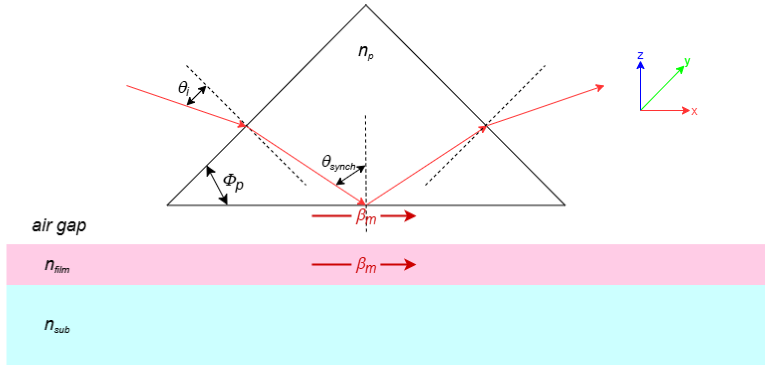
Figure 2.
Phase evolution along the structure with the relevant parameters for calculation.
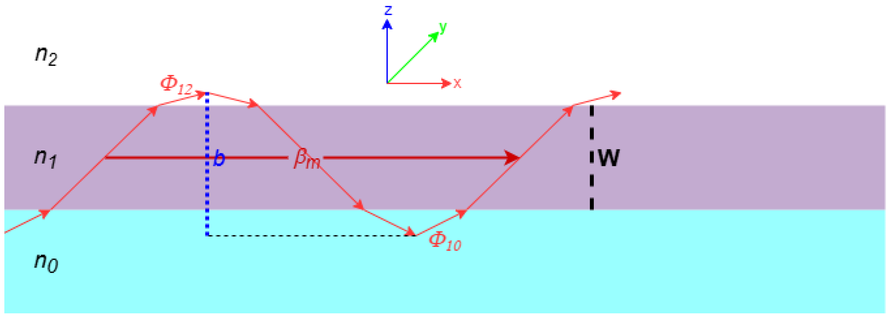
Figure 3.
Graphical display of the terms referred in previous expressions.
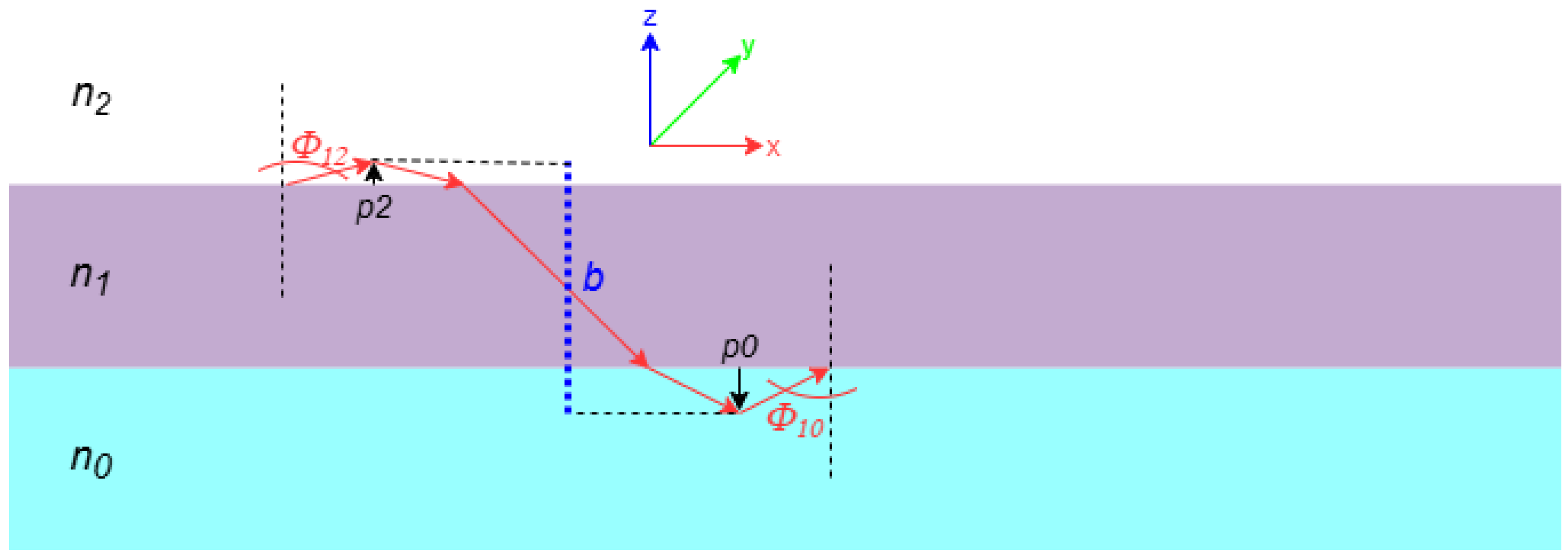
Figure 4.
TE and TM modes as a function of the width of the thin film.
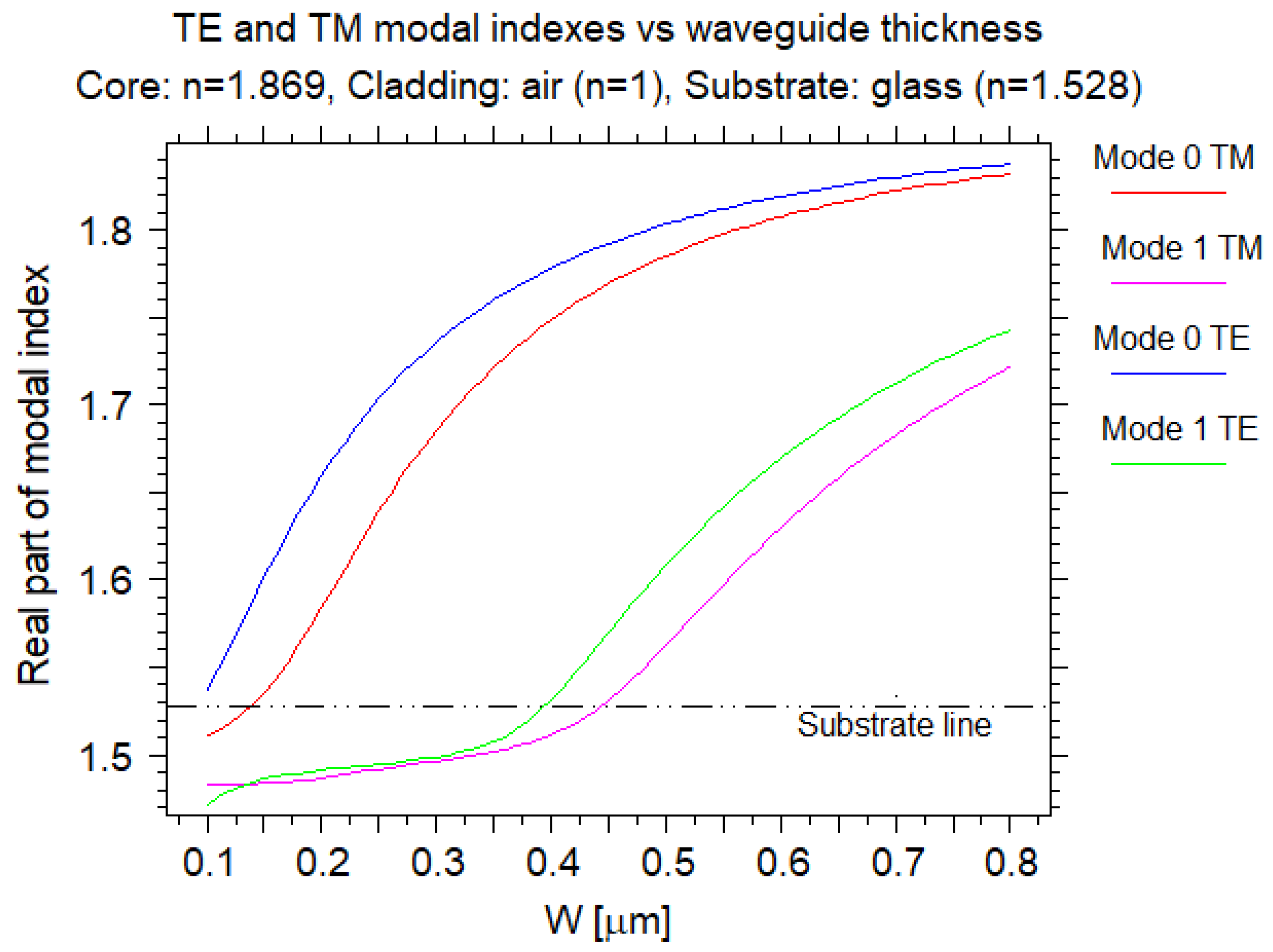
Figure 5.
Photograph of the implemented optical setup.
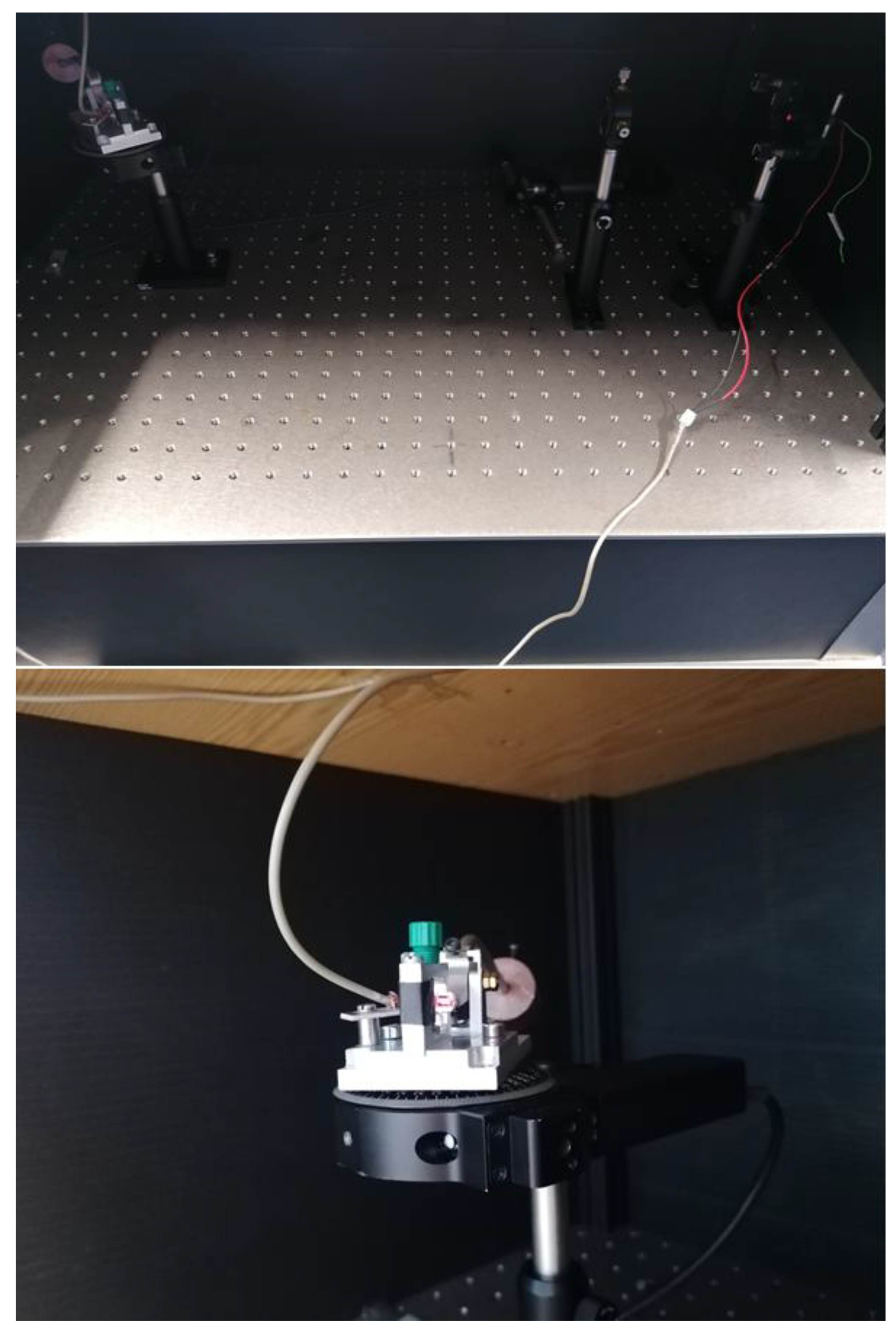
Figure 6.
Photodetector measurements, results obtained with a) parallel and b) perpendicular, polarizations.
Figure 6.
Photodetector measurements, results obtained with a) parallel and b) perpendicular, polarizations.
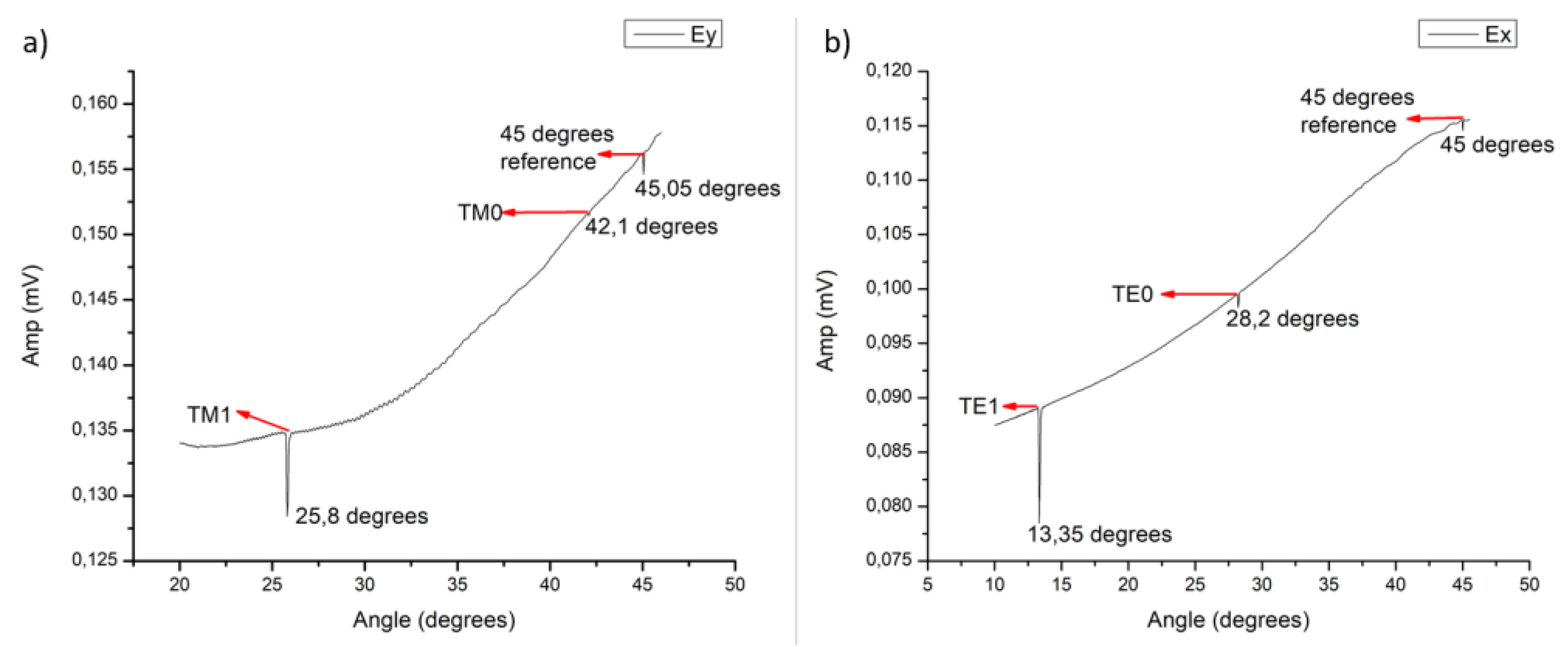
Figure 7.
Representative field profiles excited in the film; a) fundamental TE mode/semi-infinite air superstrate; b) fundamental TE mode/100 nm airgap/semi-infinite prism; c) first TM mode/semi-infinite air superstrate; d) first TM mode/100 nm airgap/semi-infinite prism.
Figure 7.
Representative field profiles excited in the film; a) fundamental TE mode/semi-infinite air superstrate; b) fundamental TE mode/100 nm airgap/semi-infinite prism; c) first TM mode/semi-infinite air superstrate; d) first TM mode/100 nm airgap/semi-infinite prism.
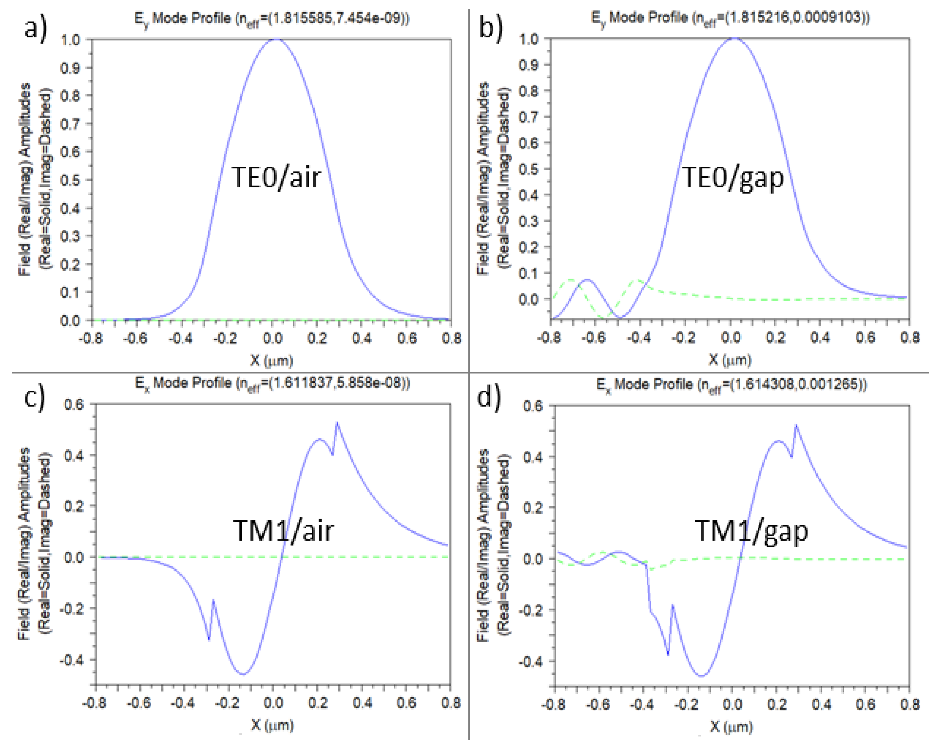

Table 1.
Results returned by the mode solver for all propagating modes in the film.
| Superstrate | Modal index | TE | TM | ||
|---|---|---|---|---|---|
| Real | Imaginary | Real | Imaginary | ||
| Semi-infinite air | 0 | 1.815585375 | 7.454358908e-09 | 1.80226624 | 4.607933757e-10 |
| 1 | 1.654669166 | -1.406253745e-07 | 1.611837029 | 5.858116836e-08 | |
| 100 nm airgap | 0 | 1.815215588 | 0.0009103236371 | 1.802696705 | 0.0001679799316 |
| 1 | 1.652140856 | 0.004189157858 | 1.614307523 | 0.00126527471 | |
Table 2.
Results obtained for the Si2C2N6 sample.
| Polarization | Film Refractive Index |
Film Thickness [m] |
|---|---|---|
| TE | 1.870445e-4 | 5.066537e-07e-11 |
| TM | 1.861256e-4 | 5.210889e-07e-10 |
Table 3.
Results obtained for the Si2C2N6 sample with a resolution of 0.01 degrees.
| Polarization | Resonant Angles | Alignment | Film | ||
|---|---|---|---|---|---|
| m = 0 | m = 1 | 45° Reference |
Refractive Index | Thickness [m] | |
| TE | 61.83e-2° | 76.69e-2° | 45e-2° | 1.869720e-4 | 5.063284e-07e-11 |
| TM | 48.03e-2° | 64.32e-2° | 45.05e-2° | 1.858736e-4 | 5.194082e-07e-11 |
Table 4.
Results obtained for the Si2C2N6 sample at an angular resolution of 0.001 degrees.
| Polarization | Resonant Angles | Alignment | Film | ||
|---|---|---|---|---|---|
| m = 0 | m = 1 | 45° Reference |
Refractive Index |
Thickness [m] | |
| TE | 61.5371e-3° | 75.3201e-3° | 44.641e-3° | 1.8643761.4e-5 | 5.330911e-078.7e-12 |
| TM | 46.7091e-3° | 62.9451e-3° | 44.641e-3° | 1.8693121.4e-5 | 5.286935e-078.6e-12 |
Table 5.
Results obtained for the Si2C2N6 sample, at an angular resolution of 0.001°, and calculated through Equation (19).
Table 5.
Results obtained for the Si2C2N6 sample, at an angular resolution of 0.001°, and calculated through Equation (19).
| Polarization | Resonant Angles |
Alignment | Film | ||
|---|---|---|---|---|---|
| 45 degrees Reference |
Refractive Index |
Thickness [m] | |||
| m = 0 | |||||
| TE | 61.5371e-3° | 44.641e-3° | 1.8532591.4e-5 | 6.063189e-078.7e-12 | |
| TM | 46.7091e-3° | 44.641e-3° | 6.047376 e-078.6e-12 | ||
Disclaimer/Publisher’s Note: The statements, opinions and data contained in all publications are solely those of the individual author(s) and contributor(s) and not of MDPI and/or the editor(s). MDPI and/or the editor(s) disclaim responsibility for any injury to people or property resulting from any ideas, methods, instructions or products referred to in the content. |
© 2025 by the authors. Licensee MDPI, Basel, Switzerland. This article is an open access article distributed under the terms and conditions of the Creative Commons Attribution (CC BY) license (http://creativecommons.org/licenses/by/4.0/).
Copyright: This open access article is published under a Creative Commons CC BY 4.0 license, which permit the free download, distribution, and reuse, provided that the author and preprint are cited in any reuse.


