Submitted:
17 November 2025
Posted:
17 November 2025
You are already at the latest version
Abstract
KY converters are interesting DC/DC converter concepts. In this paper the basic posi-tive step-up converter with limited voltage transformation ratio, two types of the neg-ative output voltage step-up converter, the negative output step-up down converter, and two types of the positive output step-up-down converter based on the KY concept are treated. The disadvantage of all these converters is a recharging current peak at all switching periods leading to stress of the components and an additional elec-tro-magnetic compatibility problem. Two methods to improve the converters are pre-sented. First an included limiting resistor reduces the spike of the recharging pulse, and second a small inductor is placed in the recharging loop making a resonant charg-ing possible, that improves the efficiency. The function of the basic converters is ex-plained and the two improvements are included. The considerations are proved by simulations and measurements of a small converter laboratory design are shown.
Keywords:
KY converter
; negative output
; positive output
; resonance
; step-up-down
; step-up
1. Introduction
In this section the so called KY converter topologies are shown. The basic aspects are analyzed by using ideal components and the continuous mode. In the simulations an input source with 0.125 Ω series resistance is used in most cases.
1.1. KY Converter
In the comprehensive study (with 309 references) [1] concerning step-up converters the basic circuit of the KY converter is given. The reference which is used is [2] and shown in Figure 1.
During the first mode M1, when the first switch S1 is on; the output current flows through the intermediate capacitor C1 and discharges it. The voltage across C1 decreases. When the switch S1 is turned off, the diode D turns on, and the current through coil commutates into the diode D. Now switch S2 can be turned on and the capacitor is recharged up to the value of the input voltage. This happens during each switching cycle. For the calculation of the voltage transformation ratio one can set the voltage across C1 constant and equal to the input voltage. With d as the duty cycle of the control signal of S1, the voltage-time balance across the coil can be written according to
leading to the voltage transformation ratio
The converter has a limited output voltage of maximum two times higher of the input voltage. An interesting aspect is the linear voltage transformation ratio. The mean value of the current through the coil is equal to the load current. Figure 2 shows the steady state. The signals shown are: the input current, the current through the coil, the load current, the output voltage, the input voltage, the voltage across C1, the control signal of switch S2, the control signal of switch S1. The recharging of the capacitor C1 leads to a large current pulse at the input and through the diode D, the capacitor C1, and the second switch S2.
1.2. Negative Output KY Boost Converter Type I
This topology can be found in [3] and the circuit diagram is shown in Figure 3. During mode M1 the switch S1 and the diode D1 are on, the diode D2 is off. The load is supplied by the capacitor C2. During this mode the current through the coil increases and the capacitor C1 is recharged up to the input voltage. When S1 is turned off, the diode D2 turns on, D1 turns off, the output capacitor C2 is charged and the intermediate capacitor C1 is discharged.
During mode M1 the switch S1 and the diode D1 are on, the diode D2 is off. The load is supplied by the capacitor C2. During this mode the current through the coil increases and the capacitor C1 is recharged up to the input voltage. When S1 is turned off, the diode D2 turns on, D1 turns off, the output capacitor C2 is charged and the intermediate capacitor C1 is discharged.
For the voltage-time balance across the inductor one gets (the voltage across C1 is always approximately equal to the input voltage)
which leads to the voltage transformation ratio
The voltage transformation ratio is equal to the one describing the normal boost converter. The advantage is that the start-up can done by slowly increasing the duty cycle from zero up to the desired value. Figure 4 shows the signals: the input current, the current through the coil L1, the load current, the input voltage, the voltage across C1, the control signal of switch S1, and the output voltage in the steady state. Again the recharge of C1 causes a high current pulse.
1.3. Negative Output KY Boost Converter Type II
A second kind of an inverting KY Boost converter is treated in [4] and shown in Figure 5. The voltage-time balance with equal voltages across the capacitors is given by
which again leads to the voltage transformation ratio
During the on-time of the active switch (during M1) two loops happen. The current through the coil increases and flows through the switch and at the same time the intermediate capacitor C1 is in parallel to the output capacitor C2, and a balancing current is flowing through the switch. The balancing current is limited by the parasitic resistors of the active switch, the differential resistor of the diode D2 and the series resistors of the capacitors. At the end of the balancing process, both capacitors now have the same voltage, the output voltage. During mode M2, when the active switch is off, D1 is on and the diode D2 is blocked. The load is supplied by the output capacitor C2 and the voltage across it decreases. The current through the coil now charges the intermediate capacitor C1.
Figure 6 shows the input current, the current through the coil L1, the load current, the input voltage, the voltage across C1, the control signal of switch S1, and the output voltage.
1.4. Inverting KY Buck-Boost Converter
This converter topology is presented in [5] and the circuit diagram is depicted in Figure 7. The converter consists of four switches which can be combined to two half-bridges, two intermediate capacitors C1 and C3, the output capacitor C2, one coil, and two diodes. During mode M1, S1 and S3 are turned on. The capacitors are now in parallel to the input voltage and are charged to this value (only the forward voltage of the diode reduces the value a little). During this mode, the current through the coil free-wheels through D2 and charges the output capacitor C2. During mode M2 the switches S2 and S4 of the two half-bridges are on. Both intermediate capacitors are now discharged by the current through the coil. The coil and the output capacitor C2 form a low-pass and smooth the output voltage. The mean current through the coil is equal to the load current, and the current through the output capacitor C2 is equal to the current ripple of the coil. No inrush current occurs, when the converter is connected to a stable input voltage and the start-up is done by increasing the duty cycle starting at zero.
Figure 8 shows the converter in the step-down modus, and Figure 9 in the step-up operation. Shown are: the input current, the current through the coil L1, the load current, the input voltage, the voltage across C1 (which is equal to the voltage across C3), the control signal of switch S1, and the output voltage.
For the voltage-time balance across the inductor one gets, with the finding that the voltage across the two capacitors must be equal, the voltage-time balance
which leads to the voltage transformation ratio
The voltage transformation ratio is limited but linear.
1.5. KY Buck-Boost Converter Type I
This type is presented in [6] and a little bit altered (S3 is here an n-channel MOSFET instead of a p-channel in the original source) and is shown in Figure 10.
The converter consists of two half-bridges connected to ground, one diode, two capacitors and one coil. During mode M1 S1 and S3 are on, the diode and the two low-side switches S2 and S4 are off. During mode M2 the high-side switches S1 and S3 are off, and the diode and the low-side switches are conducting. To obtain the voltage transformation ratio, the voltage across the coil must be taken into account. The intermediate capacitor C1 is charged to U1 during M2, when the second switch S2 is conducting. One can approximately consider the voltage across C1 equal to the input voltage. During M1 the sum of the voltage across C1 and the input voltage minus the output voltage lie across the coil; during M2 only the negative output voltage is across the coil. The voltage-time balance therefore is
leading to the linear and limited voltage transformation ratio
Figure 11 shows the input current, the current through the main coil L1, the load current, the input voltage, the voltage across C1, the control signal of switch S1, and the output voltage.
1.6. KY Buck-Boost Converter Type II
The position of the fourth switch is changed. It is not connected to ground but to the middle point of the first half-bridge. The basic literature is [6] and the circuit diagram is shown in Figure 13. S1 and S3 are on during mode M1, and the voltage across the inductor is the voltage across C1 plus the input voltage U1 minus the output voltage U2. In the second mode M2 the switches S2 and S4 are on. The diode is conducting and the intermediate capacitor C1 is recharged. Now the negative output voltage U2 is across the coil and the current through it decreases. From these considerations the same results as for variant I are achieved. The signals are shown in Figure 14.
1.7. Further Literature
The most interesting topologies are treated in the sections 1.1 till 1.6. Here some additional literature is presented. A comprehensive survey of DC-DC non-isolated topologies for unidirectional power flow in fuel cell vehicles shows 213 references including the KY concept and can be found in [7]. A comprehensive review of KY converter topologies, modulation and control approaches with their applications lists 79 references [8]. The problem of all KY converters is the charging of the intermediate capacitor directly in an Ohmic loop. As shown in section 2 this leads to losses which are independent of the resistor and a large amplitude of the recharging current occurs. It should be mentioned that in some literature instead of KY converter it is called Luo converter or super-lift converters [9,10].
2. Improvement Variant One
As shown in the introduction some types of KY converters have a linear voltage transformation ratio and a phase-minimum behavior. All of them have, however, a large current spike, when the intermediate capacitor (or capacitors) are recharged which stresses the components and can cause electromagnetic compatibility problems. This recharging also influences the efficiency of the converter.
In the converter types 2, 4 the capacitor is charged to the input voltage in mode M1, in type 3 the capacitor is charged to the output voltage, in type 4 both intermediate capacitors are charged to the input voltage. In the converters type 1, 5, 6 the recharging of the capacitor happens during mode M2. The intermediate capacitor is discharged by the value Δu during the respective other mode.
Now we study the current peak which occurs during the recharging of C1. All parasitic resistors (the series resistor of the capacitor, the differential resistor of the diode, the drain-source on-resistor of the switch, the resistor of the wiring) are summed up into R. The diode is modelled by a constant forward voltage VD and the differential resistor RD. At the end of mode M2 the capacitor is discharged to the value U1−ΔUC1. With Kirchhoff’s voltage law (KVL) one can write with the stable input voltage U1
Solving the integral equation (e.g. with the help of the Laplace calculus) leads to
The current to recharge the capacitor C1 is a large spike The voltage across C1 decreases during the first mode M1 and is always lower than the input voltage. This is caused by the forward voltage of the diode D1. The current through L1 is nearly triangular and the ripple is influenced by the value of the inductor, the input and the output voltages, and the switching frequency. To reduce the ripple a larger inductor is necessary or/and the switching frequency must be increased.
The peak current depends on the loss of the voltage during M2 and on the parasitic resistor. The time constant is the product of the resistor and the value of the capacitor. The current peak leads to loss across the resistor. The energy which is transformed into heat is the integral of the product between the current and the voltage across the resistor. When the on-time of the switch is five times or more longer, one can integrate with practically no error until infinity. So one gets for the energy which is dissipated
Multiplying the energy with the switching frequency leads to the power loss caused by the recharge of the capacitor C1
The most interesting fact is that the value of the resistor R is not of importance. The best (or even ideal) components do not reduce this loss! On the other side it is possible to insert a resistor to reduce the peak current without increasing the losses.
2.1. KY Converter
Adding an additional resistor in the loop does not reduce the efficiency, the losses are not increased, but the peak recharging current is reduced. There are four possibilities to insert the resistor (Table 1).
We insert the additional resistor in series to S2, because only the recharging current flows through it. Due to the load current no losses occur. Figure 15 shows the circuit diagram with the additional limiting resistor RLIM.
In Figure 16 the current through the first capacitor, the current through the coil, the load current, the voltages at the output, the input voltage, the voltage across C1, and the control signals of the two electronic switches are shown.
The capacitor C1 is not completely recharged. There are two possibilities to improve it. Either the capacitor or the limiting resistor must be decreased.
The peak is reduced but it is longer. The on-time of S1 must be equal or five times longer than the time constant
The resistor R is now the sum of the parasitic capacitors plus the resistor RLIM to limit the current. One gets therefore
This is an easy method with no additional losses compared to the original circuit according to Figue 3.
The same considerations are valid for the other types.
2.2. Negative Output KY Boost Converter Type I
The limiting resistor must be connected in series to the diode D1. Inserting it in series to other elements in the recharging loop would produce additional losses caused by the current through L1. Figure 17 shows the circuit diagram of the converter with the resistor RLIM to limit the current which recharges the capacitor C1. Figure 18 the signals.
Figure 18 shows the current through D1, the input voltage, the voltage across C1, the current through L1, the load current, the input voltage, the control signal, and the output voltage with current limiting resistor.
2.3. Negative Output KY Boost Converter Type II
The recharging happens during the on-time of the electronic switch, during mode M1. The limiting resistor could be placed in series to the output capacitor, however increasing the output ripple, it could be placed in series to the switch, but the current through the coil would cause additional losses. It is also not sensible to place the resistor in series to the intermediate capacitor, because the current through the coil flows through it during mode M2 and produces additional losses. It is advisable to place the limiting resistor in series to D2. The circuit diagram is depicted in Figure 19 and the current through intermediate capacitor C1, the current through the active switch, the current through L1, the input voltage, the control signal, the output voltage, and the voltage across C1 in Figure 20.
2.4. Inverting KY Buck-Boost Converter
When the upper switches S1 and S3 are on, the capacitors C1 and C3 are recharged up to the input voltage. To avoid additional losses, the limiting resistors are connected in series to the diodes D1 and D2 (Figure21). Figure 22 shows the current through the intermediate capacitor C1 (the shape through C3 is equal), the triangular current through L1, the input voltage, the voltage across C1 (the shape through C3 is equal), the control signal of the switches S1 and S3, the control signal of the switches S2 and S4, and the output voltage.
2.5. KY Buck-Boost Converter Type I
It is obvious where one has to place the limiting resistor to avoid additional losses: only in series to the second switch. The circuit diagram is depicted in Figure 23.
Figure 24 shows the current through the limiting resistor RLIM, the triangular current through L1, the output voltage, the input voltage, the voltage across C1, the control signal of the switches S1 and S3, and the control signal of the switches S2 and S4. The intermediate capacitor or the limiting resistor should be reduced. An example with reduced resistor which leads to a higher peak but to a nearly complete recharge is shown in Figure 25.
2.6. KY Buck-Boost Converter Type II
It stands to reason to insert the limiting resistor in series to the second switch S2 (Figure 26). The signals shown in Figure 27 are the current through limiting resistor RLIM, the current through L1, the output voltage, the input voltage, the voltage across C1, the control signal of S1, and the control signal of S2.
2.7. Summary
To reduce the peak current of the recharging pulse, a limiting resistor can be inserted into the recharging loop. The intermediate capacitor must be designed at such a low value that five times the time constant is shorter than the duration of the recharging, which happens in the cases described in 2.2, 2.3, 2.4 during mode M1 and in the topologies described in 2.1, 2.5, 2.6 during mode M2 and therefore lasts (1-d)⋅T.
3. Improvement Variant 2
Charging a capacitor by connecting it directly to a voltage source or to another capacitor leads to losses, independent of the parasitic resistor which is in the loop. The smaller the resistor the higher the current peak and the shorter the charging time. A better method is to charge the capacitor via an inductor. This additional resonant coil is much smaller the main coil.
From the angular resonant frequency of a resonant circuit
one can calculate the duration of a half-wave. Within this time the capacitor is charged up again. The time for recharging must be therefore (this is during mode M1 or mode M2 depending on the circuit topology) longer than
With a given intermediate capacitor one can dimension the resonant inductor according to
For the converters 3.2, 3.3, 3.4 the recharge time is (dT) and for the converters 3.1, 3.5, and 3.6 it is (1-dT).
3.1. KY Converter
The resonant inductor L1 can be placed in series to the input or in series to the auxiliary switch S2 as shown in Figure 28. The results are the same, so only the simulation of the first variant is shown in Figure 29.
Figure 29 shows the input current, the current through the second switch, the current through the main coil L2, the output voltage, the voltage across the intermediate capacitor, the input voltage, the control signal of switch S2, the control signal of switch S1. When S2 is turned on, the resonance between C1 and L2 begins. The second transistor is turned off after the resonance current changes its sign. The body diode of the MOSFET S2 turns on, and when the main switch S1 turns on again the body diode of S2 turns off. Contrary to the concept with the limiting resistor, where the voltage reaches a value a little lower (caused by the forward voltage of the diode D, the voltage across C1 rings around the input voltage reduced by the forward voltage of the diode D.
3.2. Improved Negative Output KY Boost Converter
This converter has several interesting features: it needs only one active switch, the start-up is easy by increasing the duty cycle starting from zero, and no inrush current occurs.
To damp the recharging pulse, an inductor L2 has to be placed in series to the diode D1. The circuit diagram is depicted in Figure 30.
When S1 is turned on, the resonance circuit consisting of C1 and L2 is applied to the input voltage, and a resonance current starts to flow. When this current reaches zero, the diode D1 stops the resonance current. In Figure 31 a simulation is shown. The signals are the current through the active switch, which is equal to the input current, the current through the main coil L1, the voltage across the intermediate capacitor (dark blue), the input voltage, the control signal of the active switch S1, and the output voltage.
3.3. Improved Negative Output KY Boost Converter Type II
The resonant inductor L2 is connected in series to the second diode D2 to form a resonant circuit with C1 during mode M1. The circuit diagram can be seen in Figure 32.
When the transistor is turned on, the current through the main coil increases linearly, the intermediate capacitor is discharged by a resonant current, and energy is transferred to the output. When the resonant current is zero again, diode D2 turns off. When the switch turns off, the current through the coil commutates into the intermediate capacitor C1 and into the diode D1. The capacitor is charged and the current through the main coil L1 decreases.
Figure 33 shows a simulation. The signals are: the current through the intermediate capacitor C1, the current through the first diode, the current through the resonant coil L2 which is equal to the current through the second diode D2; the current through the main coil L1, the input voltage, the control signal of the switch, the voltage across the intermediate capacitor, the output voltage.
3.4. Improved Inverting KY Buck-Boost Converter
Here two resonance inductors L2 and L3 are necessary and have to be placed in series to the diodes D1 and D2, shown in the circuit diagram Figure 34. During M1 both intermediate capacitors are charged in a resonant way and the voltages across C1 and C3 increase. The current through the main coil L1 decreases. When the resonant current reaches zero, the respective diodes D1 or D2 turns off. The voltage across the main coil L1 is still negative and the current through it decreases until the high side switches S1 and S3 are turned off and the switches S2 and S4 turn on. Now a positive voltage is across the main inductor and the current through it increases. Figure 35 shows the input current, the current through the diode D1, the current through the main coil L1, the voltage across the intermediate capacitor, the input voltage, the control signal of the switches S2 and S4, the control signal of the switches S1 and S3, and the output voltage.
3.5. Improved KY Buck-Boost Converter Type I
The limiting resistor of the converter 2.5 is replaced by the resonant inductor and the new circuit diagram is depicted in Figure 36. A typical system behavior is shown in Figure 37, where the input current, the current through the main coil L1, the output voltage, the voltage across the intermediate capacitor, the input voltage, the control signal of the switches S2 and S4, and the control signal of the switches S1 and S3 are shown.
3.6. Improved KY Buck-Boost Converter Type II
4. Conclusion
Two methods to improve the KY converter are treated in this paper. Six converter topologies are presented:
1 the basic KY converter
2 the negative output KY Boost converter type I
3 the negative output KY Boost converter type II
4 the inverting KY Buck-Boost converter
5 the KY Buck-Boost converter type I
6 the KY Buck-Boost converter type II
The voltage transformation ratio is 1+d for type 1, 1/(1-d) for types 2 and 3, 2(1-d) for type 4, 2d for types 5 and 6. Type 2 has the same voltage transformation ratio as the classical Boost converter, however, the output voltage is inverse to the input voltage. All other types have a linear voltage transformation ratio depending on the duty cycle. It can be shown that this linearization is combined with a phase-minimum behavior. So, all these converters have no zeroes on the right side of the complex plane, and the phase shift is reduced compared to converters with zeroes on the right side.
The converters which have switches directly in series with the input source (2), and the converters with half-bridges (4, 5, 6) have no inrush current and the start-up can be done by increasing the duty cycle starting from zero. Only the classical KY converter (1) and the negative output KY Boost converter II (3) show an inrush current when connected to a stable input source. It is advisable to use converter 2 instead of converter 3. All these converters have the disadvantage of a large current pulse, when the intermediate capacitor (or capacitors) is (are) recharged. This happens in every switching period. It is shown that the losses caused by this recharging are independent of the resistor in the loop. Therefore, one can include an additional resistor in the recharging loop, which reduces the current peak without changing the losses. This is demonstrated in section 2. A better solution is demonstrated in section 3. Here the recharging happens in a resonant way. Now losses occur only by the parasitic resistors and depend on these. Ideal components would lead to no losses, because the energy transfer goes over the magnetic field.
The intermediate capacitor is charged to a fix voltage during each switching cycle, and the additional inductor reaches zero in each cycle. Therefore, the dynamics of the converter are determined only by the main inductor and the output capacitor. The small signal model is only of second order and is easier to control than a third or a fourth order system.
The circuits are useful for application with small step-up ratios.
Author Contributions
FH wrote the text, made the figures and did the simulations. HV did the prove reading, built the converter and did the measurements.
Funding
This research received no external funding.
Data Availability Statement
all data are included in the paper.
Conflicts of Interest
The authors declare no conflicts of interest.
Appendix A
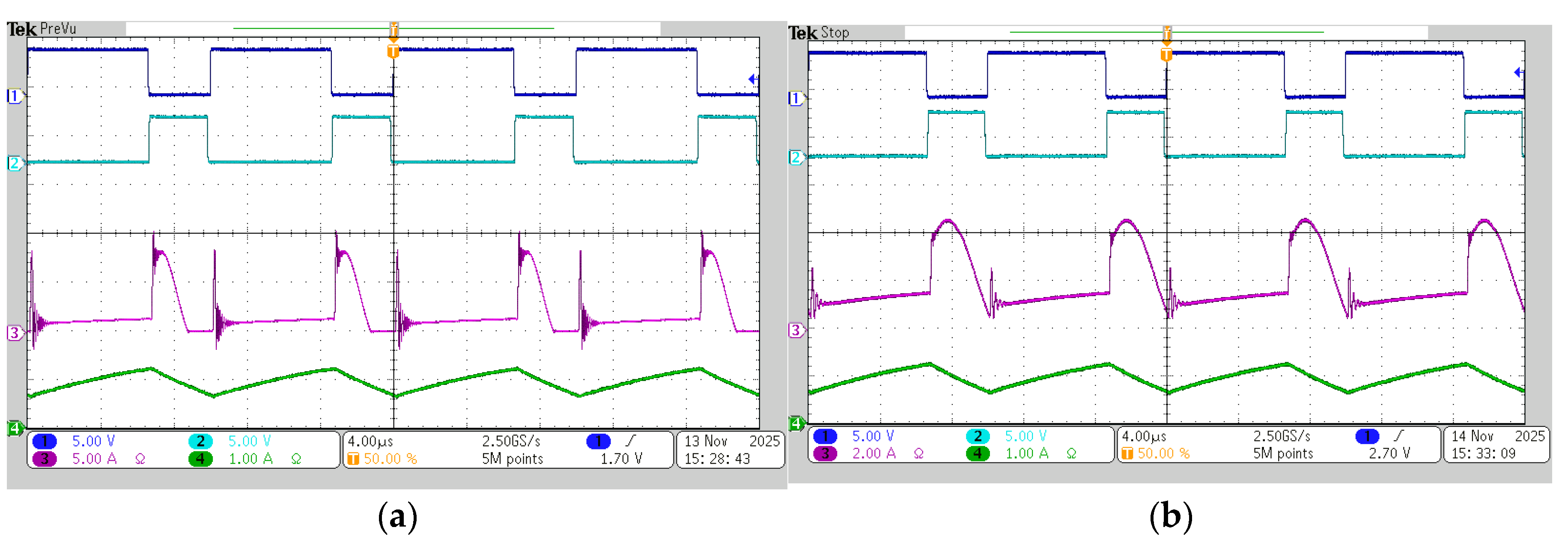
Measurement of a laboratory model of the KY converter with additional coil (c.f. 3.1)
Figure A1.
control signal of switch S2, input current, current through the main inductor (a) load 10 Ω; (b) load 20 Ω.
Figure A1.
control signal of switch S2, input current, current through the main inductor (a) load 10 Ω; (b) load 20 Ω.
References
- Forouzesh, M.; Siwakoti, Y. P.; Gorji, S. A.; Blaabjerg, F.; Lehman, B. A survey on voltage boosting techniques for step-up DC-DC converters. In 2016 IEEE Energy Conversion Congress and Exposition (ECCE), Milwaukee, WI, USA, 2016, pp. 1-8. [CrossRef]
- Hwu, K. I.; Yau, Y. T. KY Converter and Its Derivatives. IEEE Transactions on Power Electronics, vol. 24, no. 1, pp. 128-137, Jan. 2009. [CrossRef]
- Hwu, K. I.; Tu, W. C.; Chen, Y. H. A novel negative-output KY boost converter. In 2009 International Conference on Power Electronics and Drive Systems (PEDS), Taipei, Taiwan, 2009, pp. 1155-1157. [CrossRef]
- K. I.; Chen, Y. H.; Tu, W. C. Negative-output KY boost converter. In 2009 IEEE International Symposium on Industrial Electronics, Seoul, Korea (South), 2009, pp. 272-274. [CrossRef]
- Hwu, K. I.; Lin, Z. F.; Chen, Y. H. A novel negative-output KY buck-boost converter. In 2009 International Conference on Power Electronics and Drive Systems (PEDS), Taipei, Taiwan, 2009, pp. 1158-1162. [CrossRef]
- Hwu, K. I.; Yau, Y. T. Two Types of KY Buck–Boost Converters. IEEE Transactions on Industrial Electronics, vol. 56, no. 8, pp. 2970-2980, Aug. 2009. [CrossRef]
- Sagar Bhaskar, M.; Ramachandaramurthy, V. K.; Padmanaban, S.; Blaabjerg, F.; Ionel, D. M.; Mitolo, M.; Almakhles, D. Survey of DC-DC Non-Isolated Topologies for Unidirectional Power Flow in Fuel Cell Vehicles. IEEE Access, vol. 8, pp. 178130-178166, 2020. [CrossRef]
- Kumar, K. R.; Raja, K. R.; Padmanaban, S.; Muyeen, S. M.; Khan, B. Comprehensive Review of KY Converter Topologies, Modulation and Control Approaches with Their Applications. IEEE Access, vol. 10, pp. 20978-20994, 2022. [CrossRef]
- Luo, F. L.; Ye, H. Negative output super-lift converters. IEEE Transactions on Power Electronics, vol. 18, no. 5, pp. 1113-1121, Sept. 2003. [CrossRef]
- Luo, F. L. Six self-lift DC-DC converters, voltage lift technique. IEEE Transactions on Industrial Electronics, vol. 48, no. 6, pp. 1268-1272, Dec. 2001. [CrossRef]
- Himmelstoss, F. Inverting step-up converter, in German invertierender Hochsetzer, Austrian patent AT 525632 B, filled 2022/04/20, published 2023/06/15.
Figure 1.
Basic KY converter.
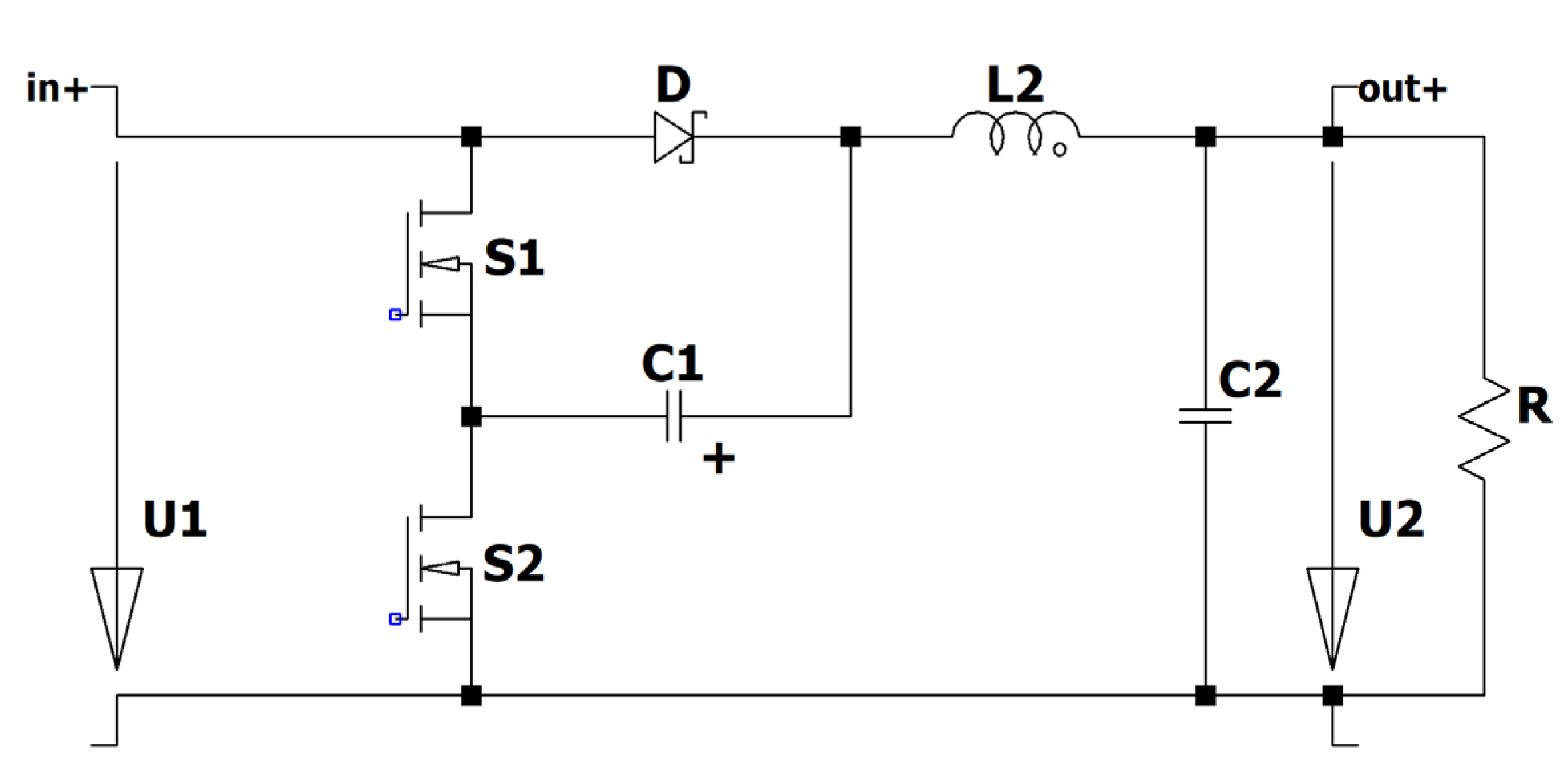
Figure 2.
KY converter (a) simulation circuit; (b) top to bottom: input current (violet); current through the coil LH (red), load current (brown); output voltage (green), input voltage (blue), voltage across C1 (dark blue), control signal of switch S2 (dark green, shifted), control signal of switch S1 (turquoise).
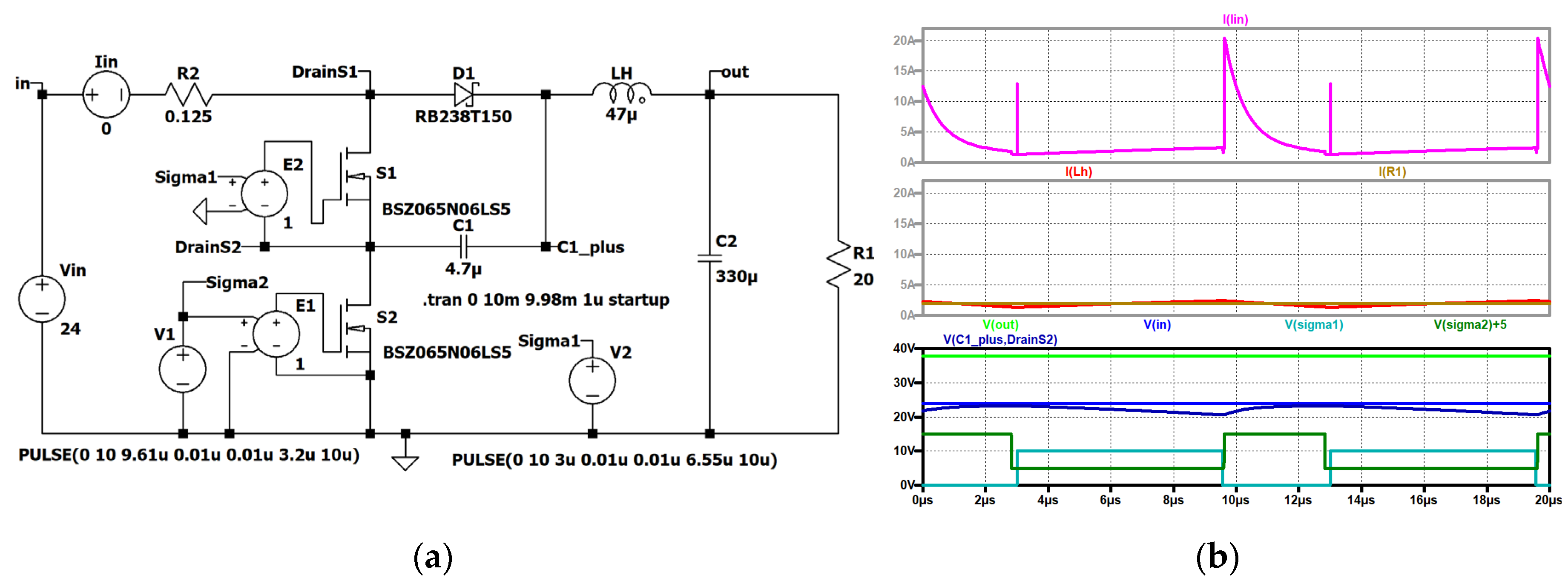
Figure 3.
Negative output KY boost converter type I.
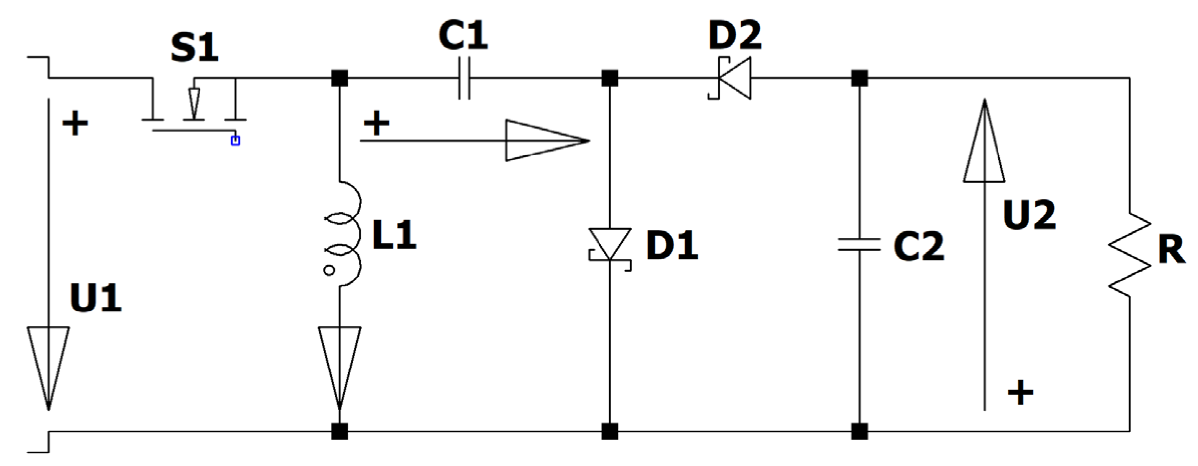
Figure 4.
Negative output KY Boost converter type I: (a) simulation circuit; (b) top to bottom: input current (violet); current through the coil L1 (red), load current (brown); input voltage (blue), voltage across C1 (dark blue), control signal of switch S1 (turquoise), output voltage (green).
Figure 4.
Negative output KY Boost converter type I: (a) simulation circuit; (b) top to bottom: input current (violet); current through the coil L1 (red), load current (brown); input voltage (blue), voltage across C1 (dark blue), control signal of switch S1 (turquoise), output voltage (green).
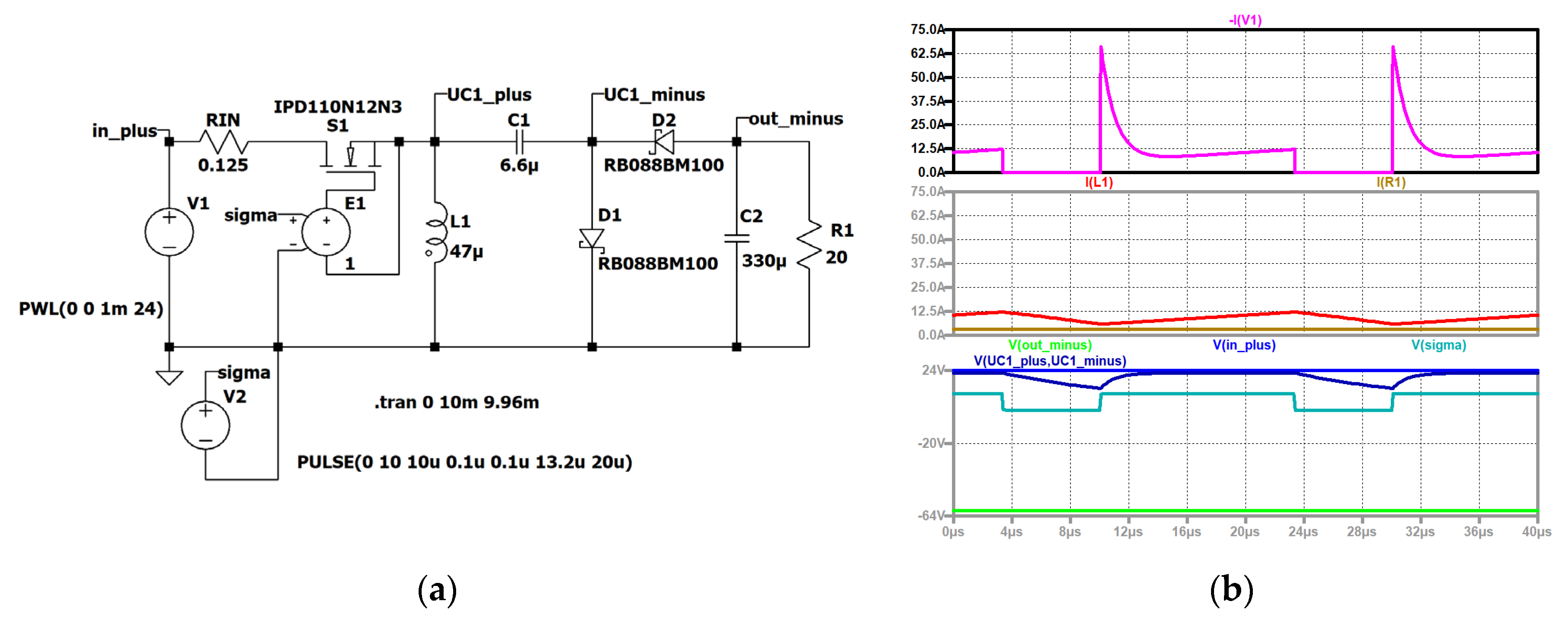
Figure 5.
Negative output KY Boost converter type II.
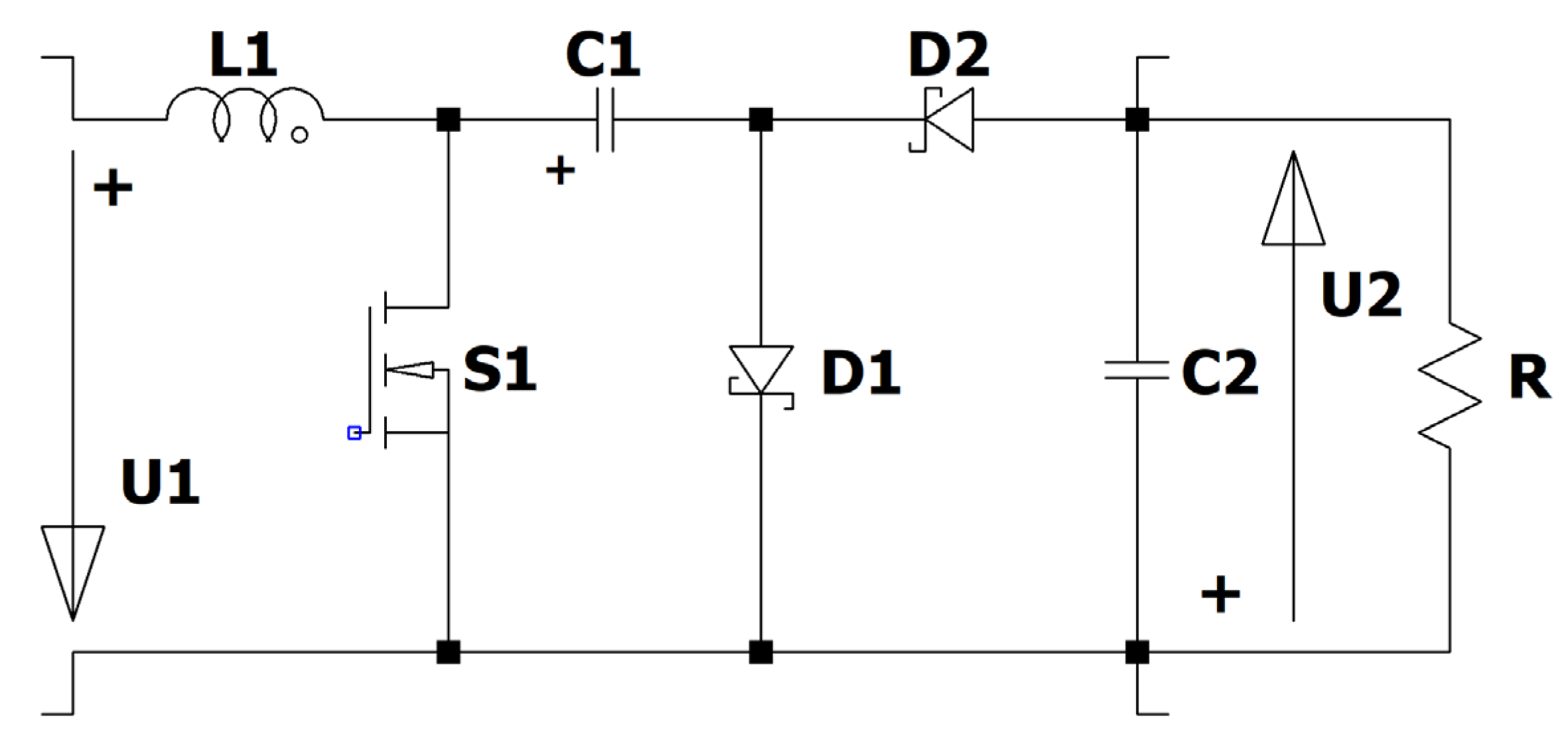
Figure 6.
Negative output KY Boost converter type II: (a) simulation circuit; (b) top to bottom: input current (violet); current through the coil L1 (red), load current (brown); voltage across C1 (dark blue), input voltage (blue), control signal of switch S1 (turquoise), output voltage (green).
Figure 6.
Negative output KY Boost converter type II: (a) simulation circuit; (b) top to bottom: input current (violet); current through the coil L1 (red), load current (brown); voltage across C1 (dark blue), input voltage (blue), control signal of switch S1 (turquoise), output voltage (green).
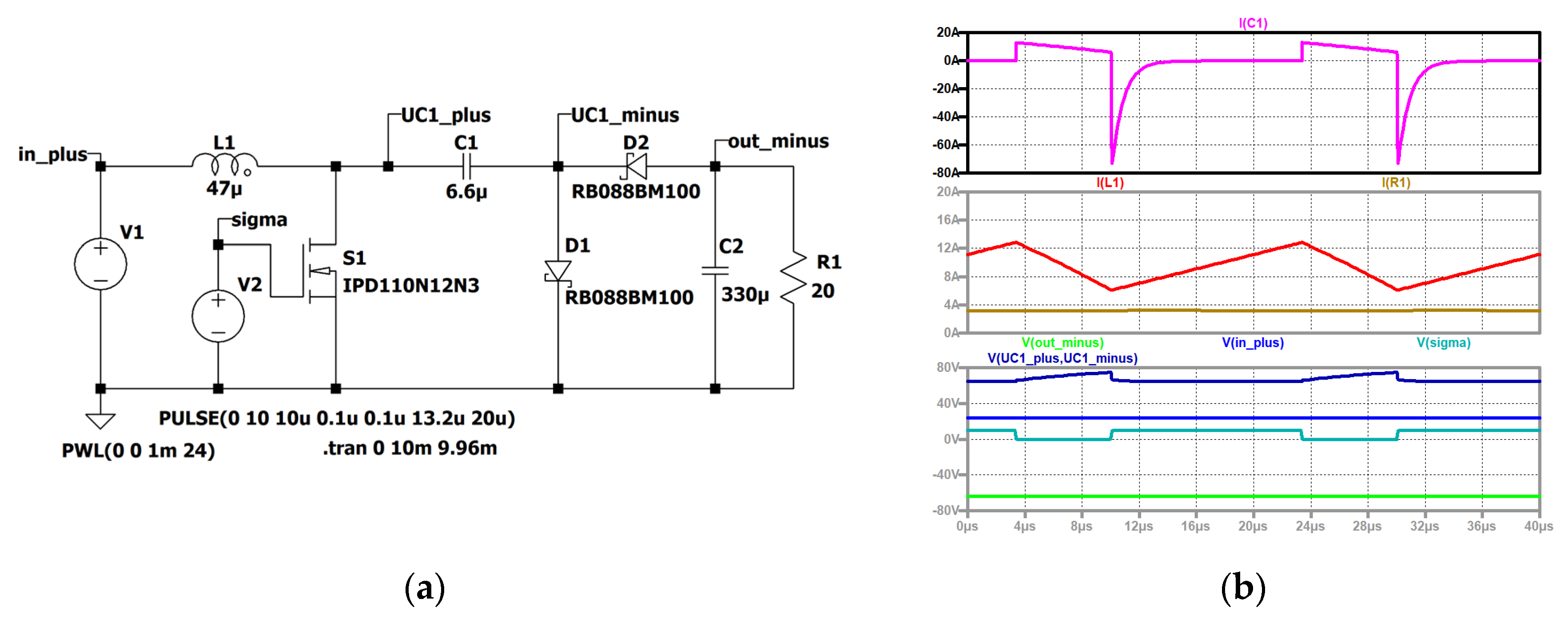
Figure 7.
Inverting KY Buck-Boost converter.
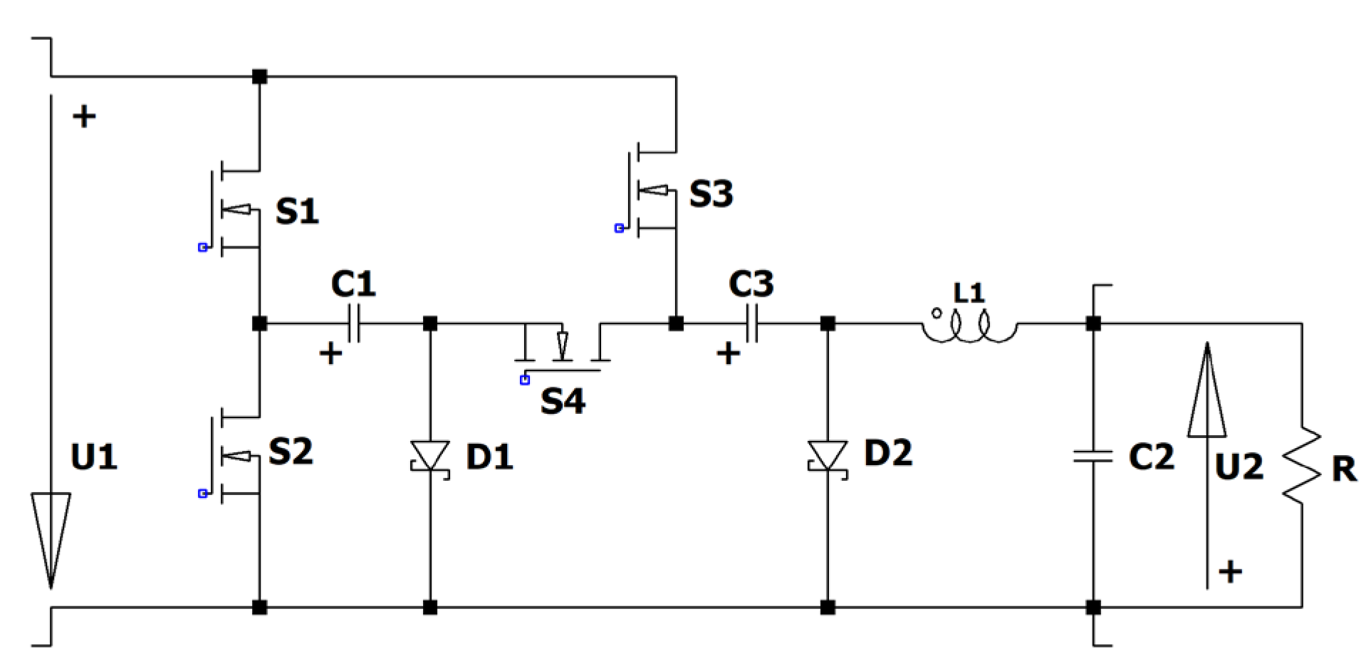
Figure 8.
Inverting KY Buck-Boost converter in step-down mode: (a) simulation circuit; (b) top to bottom: input current (violet); current through the coil L1 (red), load current (brown); input voltage (blue), voltage across C1 (dark blue), control signal of switch S1 (turquoise), output voltage (green).
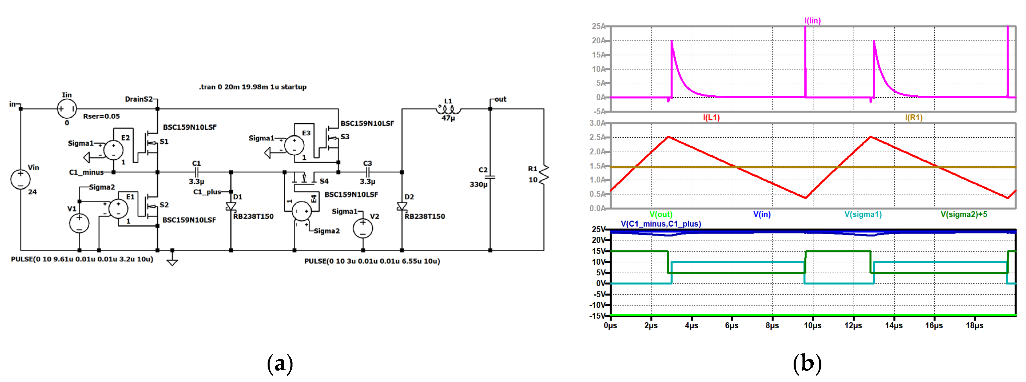
Figure 9.
Inverting KY Buck-Boost converter in step-up mode: (a) simulation circuit; (b) top to bottom: input current (violet); current through the coil L1 (red), load current (brown); input voltage (blue), voltage across C1 (dark blue), control signal of switch S1 (turquoise), output voltage (green).
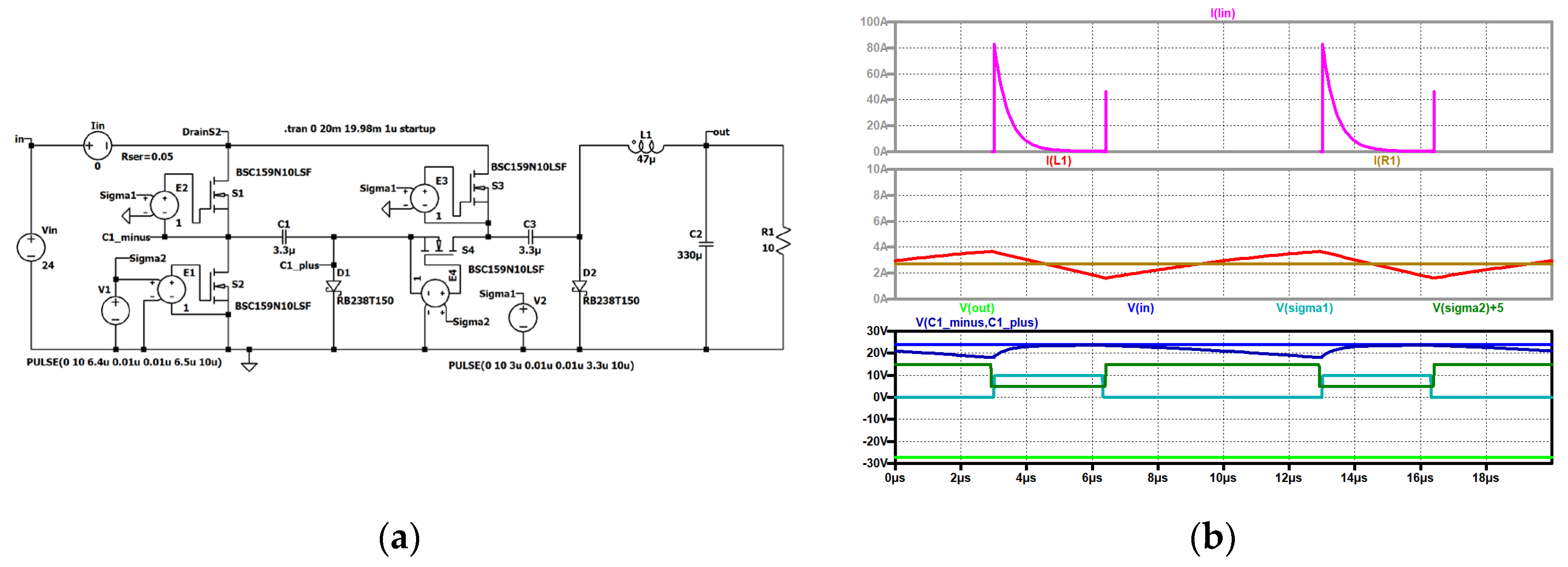
Figure 10.
KY Buck-Boost converter type I.
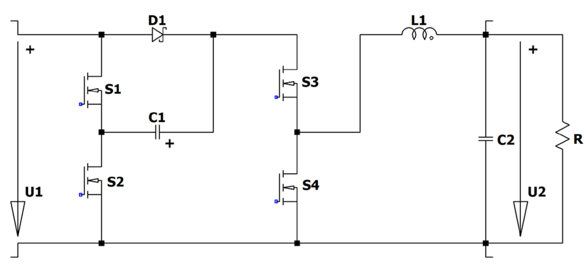
Figure 11.
KY Buck-Boost Converter type I: (a) simulation circuit; (b) top to bottom: input current (violet); current through the coil L1 (red), load current (brown); input voltage (blue), voltage across C1 (dark blue), control signal of switch S1 (turquoise), output voltage (green).
Figure 11.
KY Buck-Boost Converter type I: (a) simulation circuit; (b) top to bottom: input current (violet); current through the coil L1 (red), load current (brown); input voltage (blue), voltage across C1 (dark blue), control signal of switch S1 (turquoise), output voltage (green).
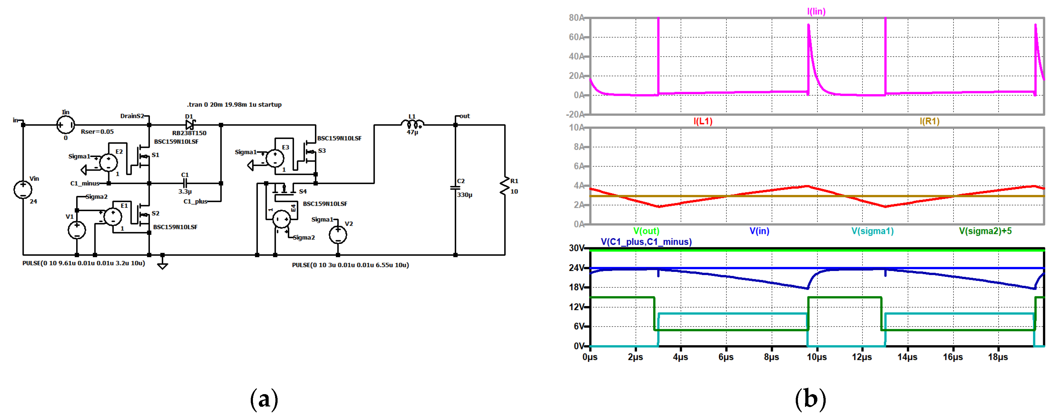
Figure 12.
KY Buck-Boost Converter type I, S4 replaced by a diode: (a) simulation circuit; (b) top to bottom: input current (violet); current through the coil L1 (red), load current (brown); input voltage (blue), voltage across C1 (dark blue), control signal of switch S1 (turquoise), output voltage (green).
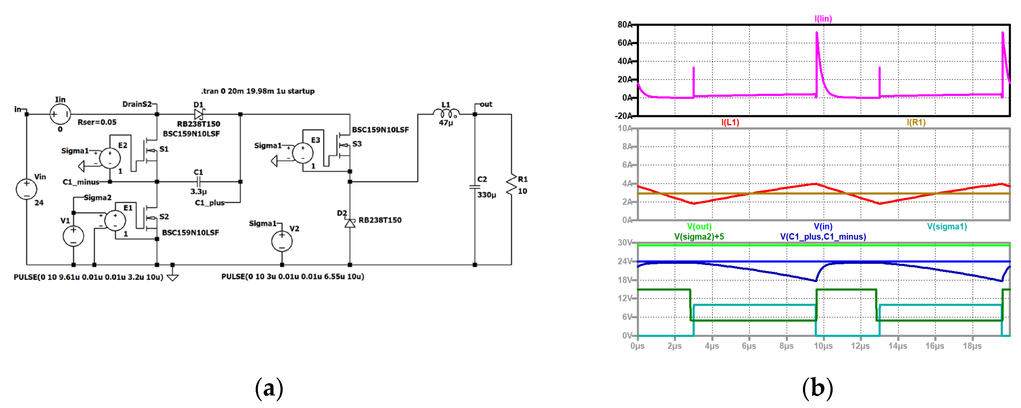
Figure 13.
KY Buck-Boost converter type II.
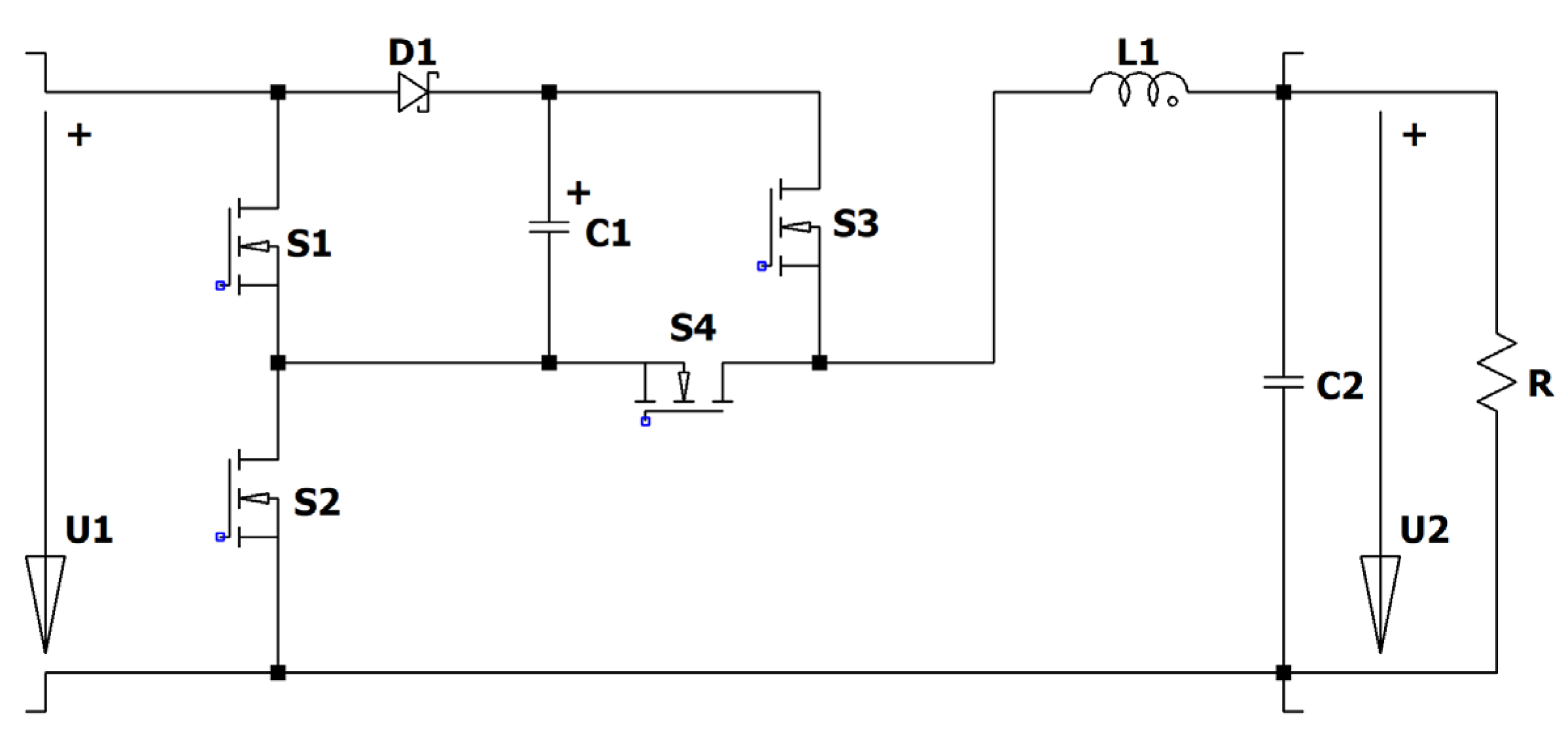
Figure 14.
KY Buck-Boost Converter type II: (a) simulation circuit; (b) top to bottom: input current (violet); current through the coil L1 (red), load current (brown); input voltage (blue), voltage across C1 (dark blue), control signal of switch S1 (turquoise), output voltage (green).
Figure 14.
KY Buck-Boost Converter type II: (a) simulation circuit; (b) top to bottom: input current (violet); current through the coil L1 (red), load current (brown); input voltage (blue), voltage across C1 (dark blue), control signal of switch S1 (turquoise), output voltage (green).
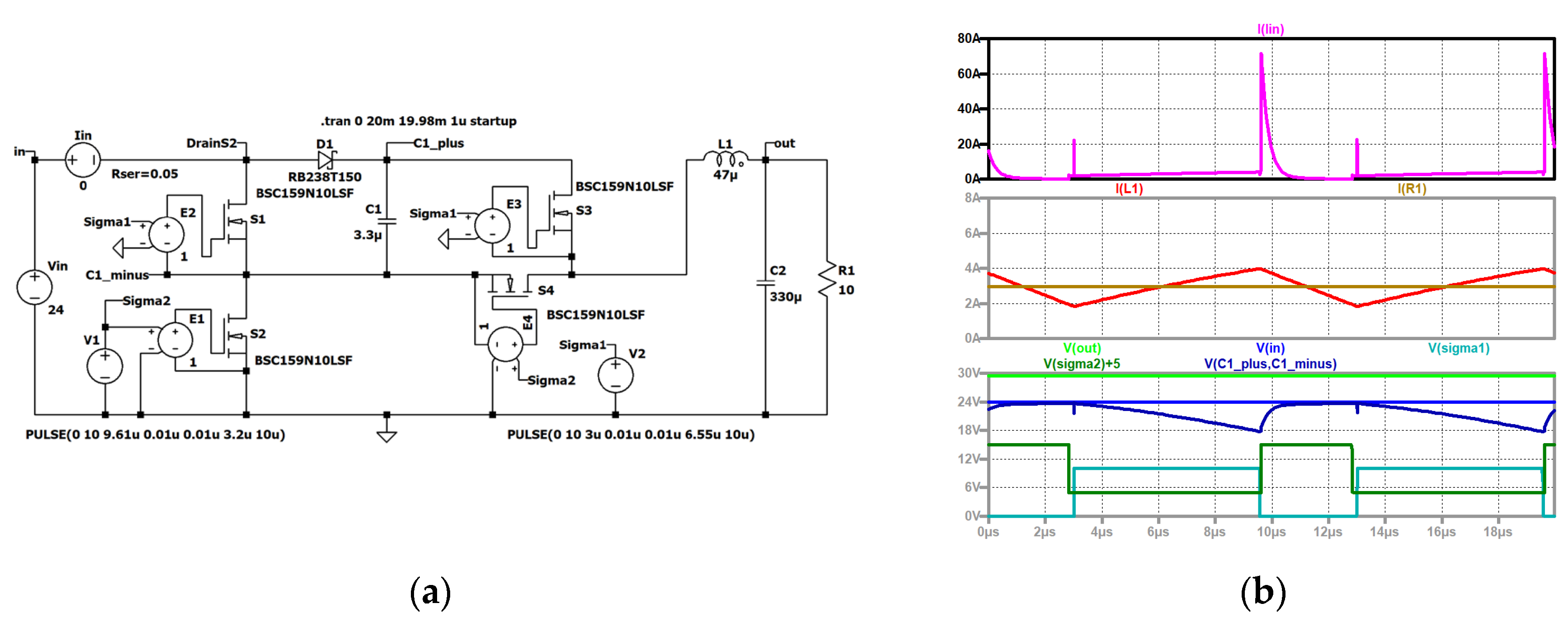
Figure 15.
KY converter with additional current limiting resistor.
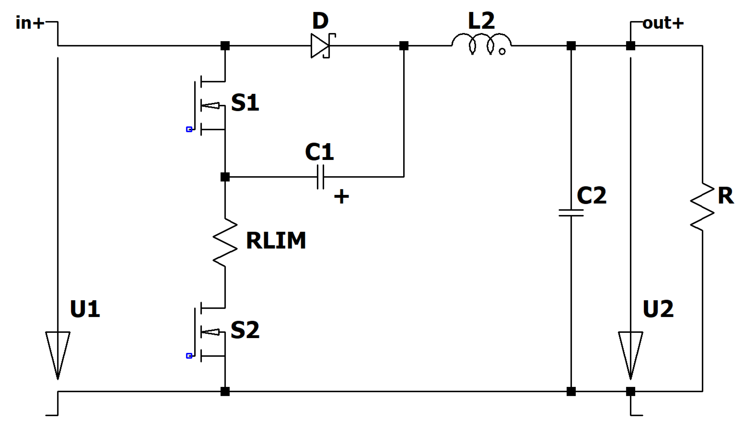
Figure 16.
KY converter with additional current limiting resistor: (a) simulation circuit; (b) up to down: current through the first capacitor (violet); current through the coil (red), load current (brown); output voltage (green), input voltage (blue), voltage across C1 (grey), control signal of the second electronic switch S2 (dark green), control signal of the first electronic switch S1 (turquoise).
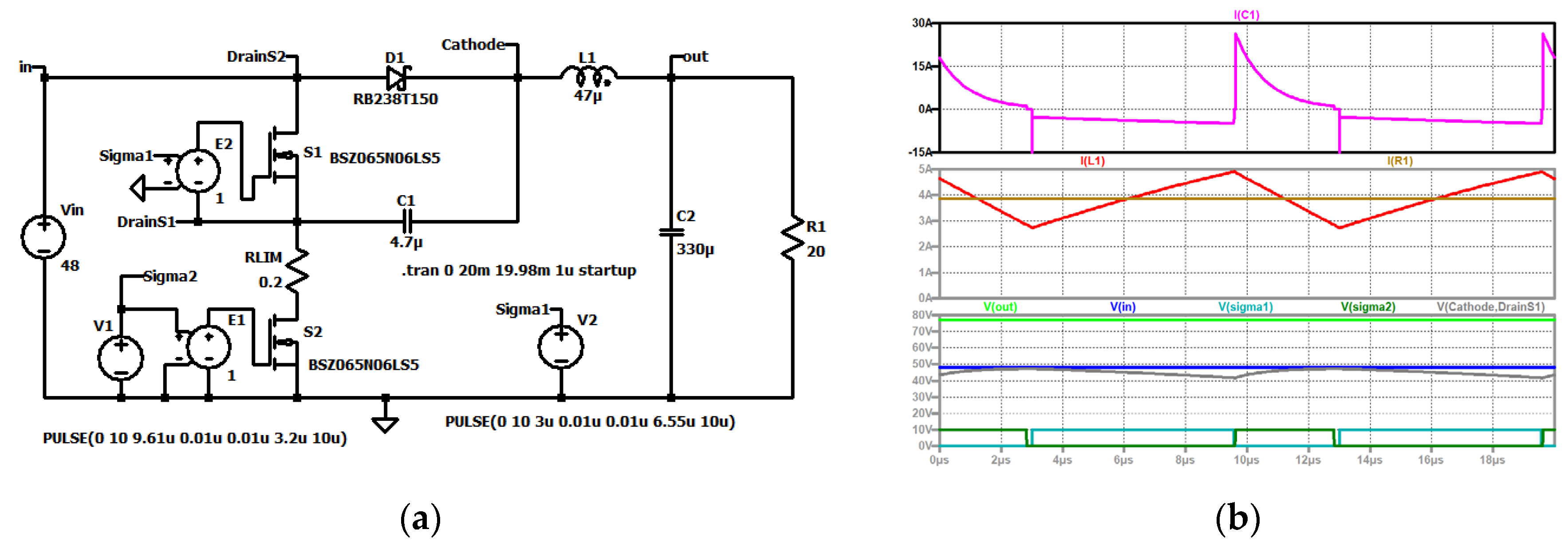
Figure 17.
Inverting KY Boost converter type 1 with limiting resistor.
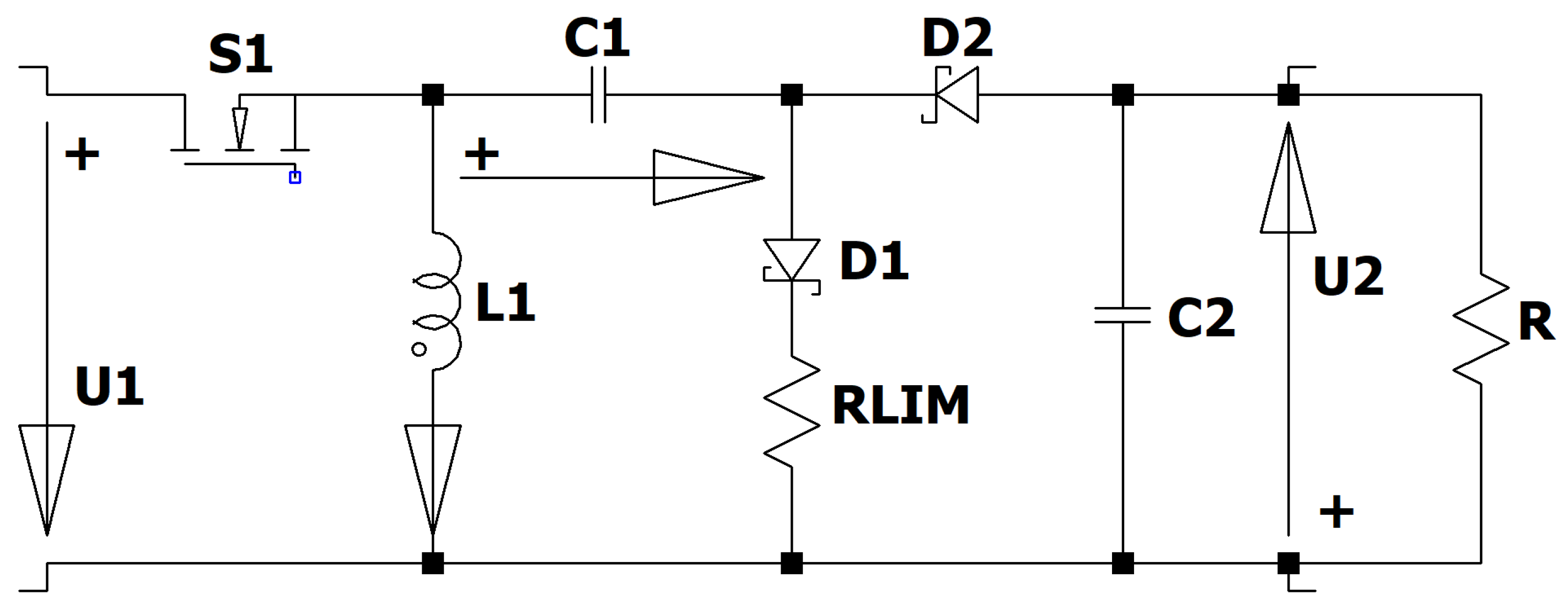
Figure 18.
Inverting KY Boost converter with limiting resistor type I: (a) simulation circuit; (b) top to bottom: current through D1 (violet); input voltage (blue), voltage across C1 (grey); current through L1 (red), load current (brown); input voltage (blue), control signal (turquoise), output voltage (green).
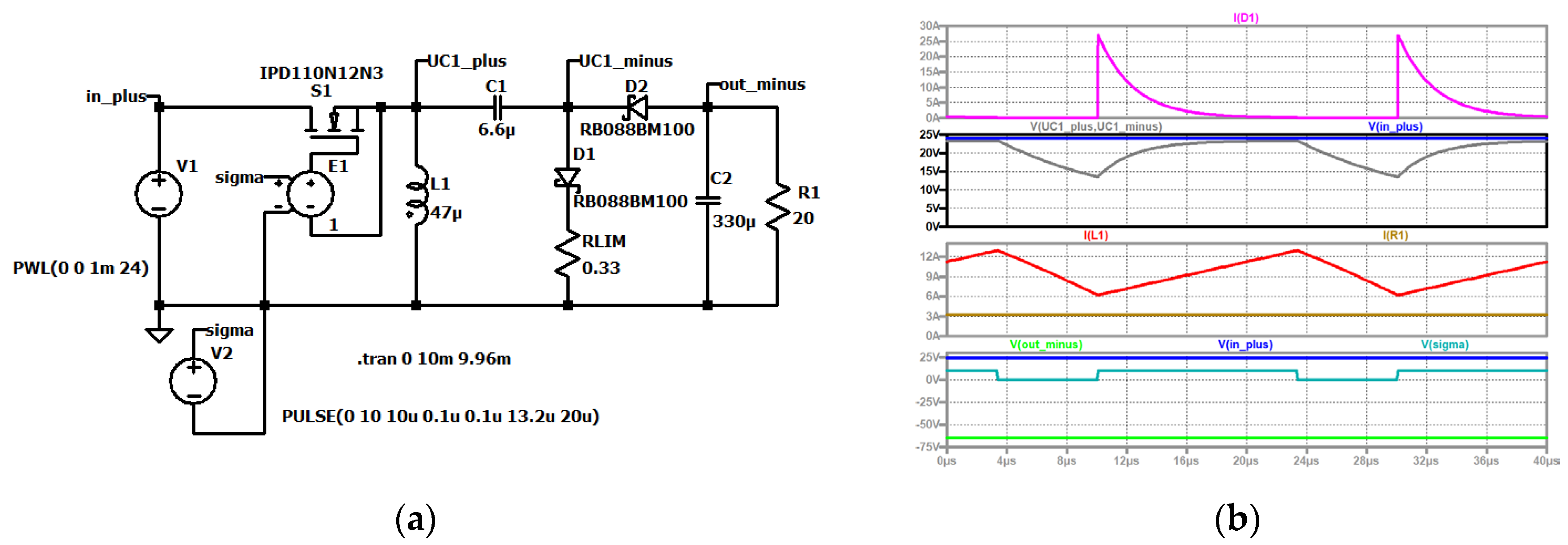
Figure 19.
Inverting KY Boost converter type II with limiting resistor.
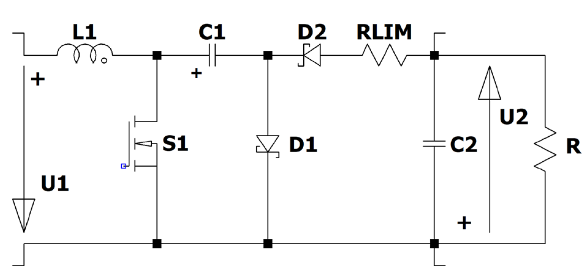
Figure 20.
Negative inverting KY Boost converter type II with limiting resistor: (a) simulation circuit; (b) up to down: current through intermediate capacitor C1 (violet); current through the active switch (grey), current through L1 (red); input voltage (blue), control signal (turquoise), output voltage (green), voltage across C1 (dark blue).
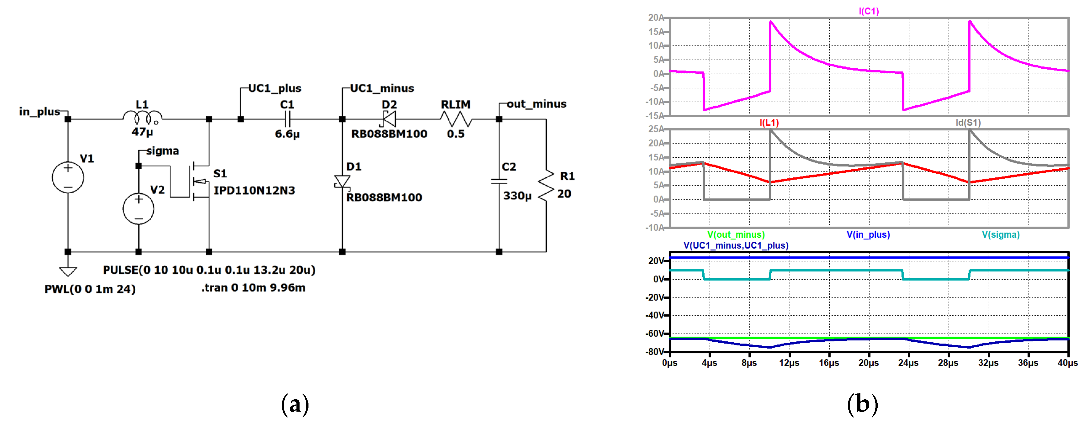
Figure 21.
Inverting KY Buck-Boost converter type II with limiting resistor.
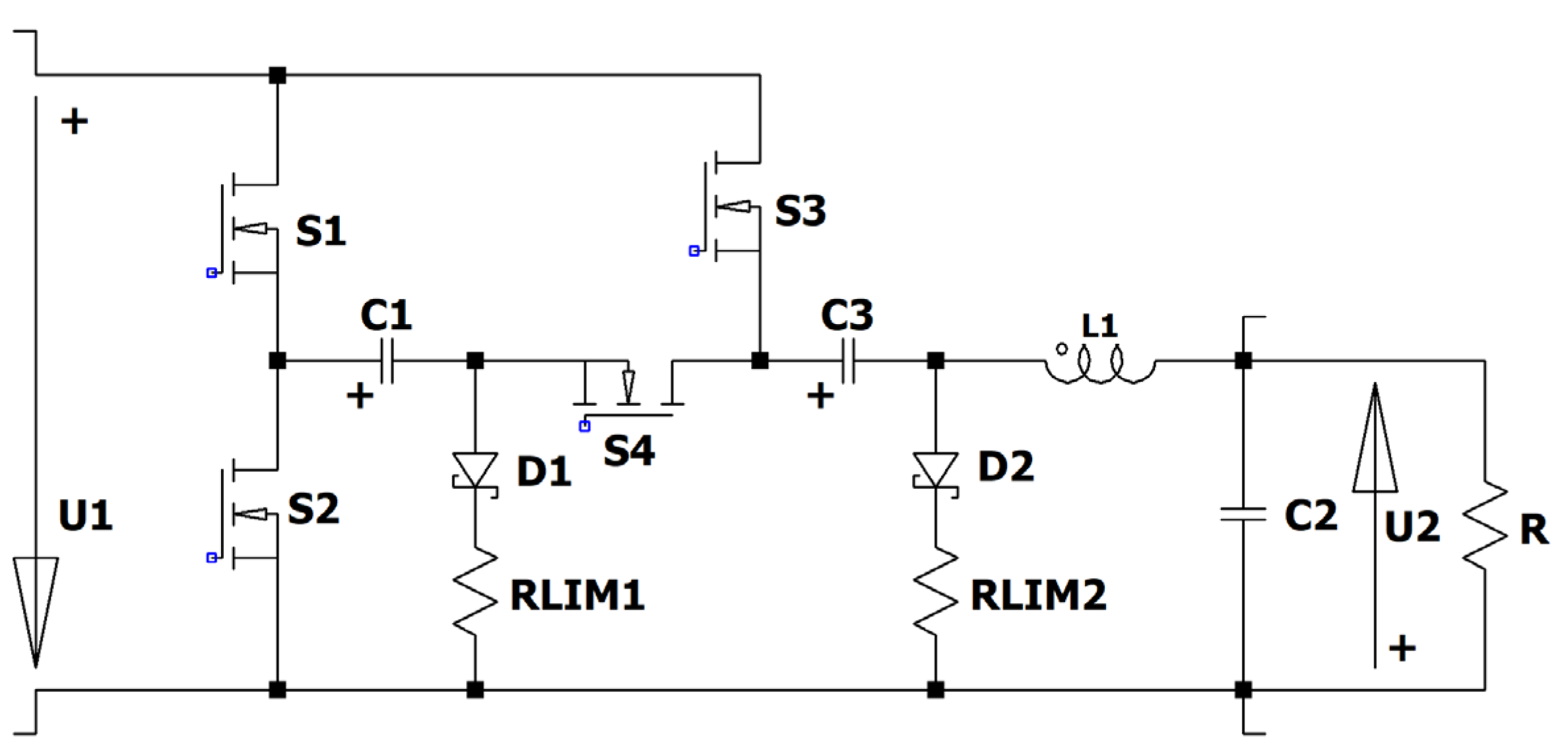
Figure 22.
Inverting KY Buck-Boost converter type II with limiting resistor: (a) simulation circuit; (b) up to down: current through intermediate capacitor C1 (violet); current through L1 (red); input voltage (blue), voltage across C1 (dark blue), control signal of S1 and S3 (turquoise), control signal of S2 and S4 (dark green), output voltage (green).
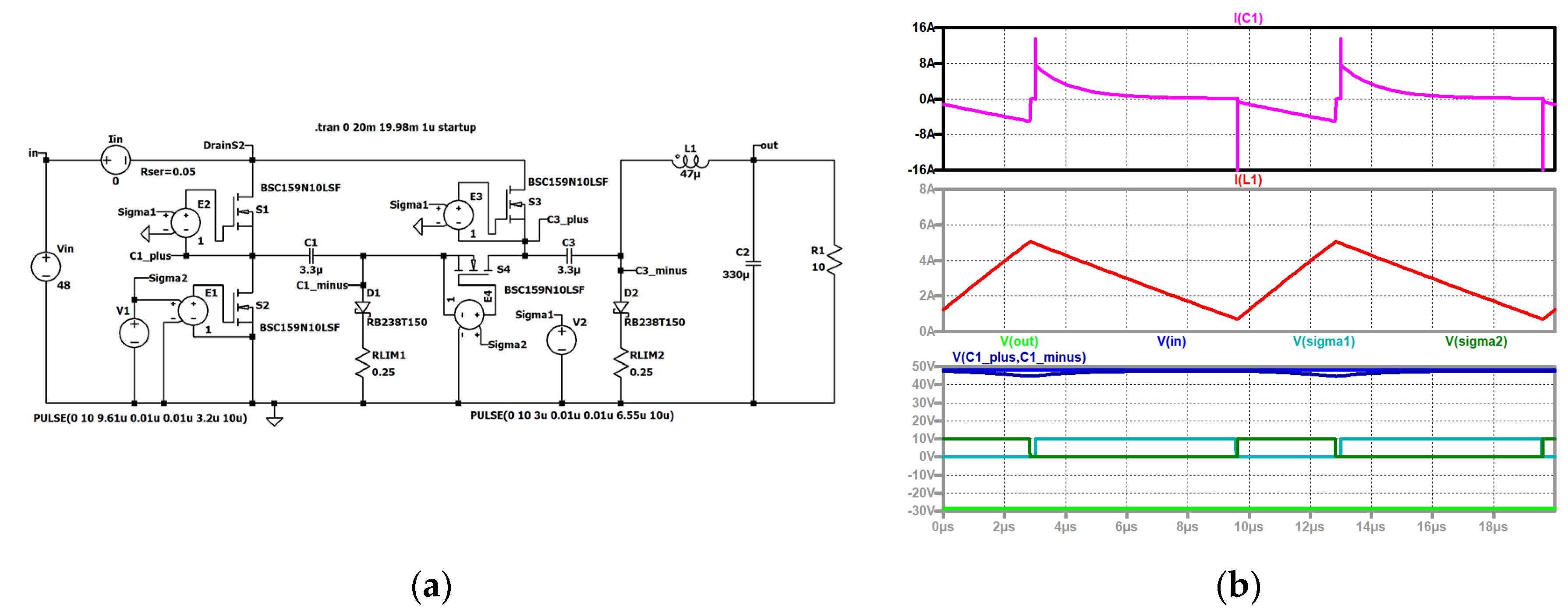
Figure 23.
KY Buck-Boost converter type I with limiting resistor.
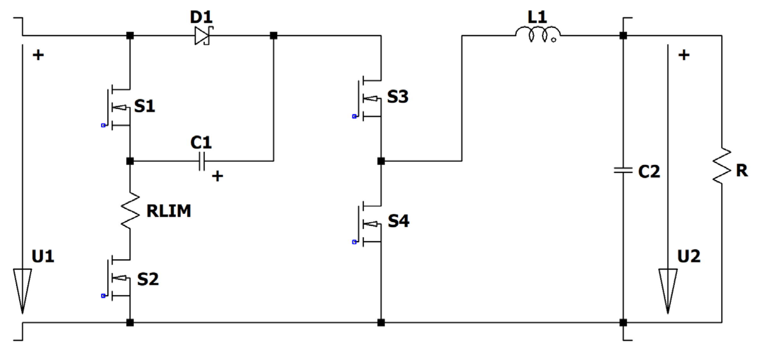
Figure 24.
KY Buck-Boost converter type I with limiting resistor: (a) simulation circuit; (b) up to down: current through the limiting resistor RLIM (grey); current through L1 (red); output voltage (green), input voltage (blue), voltage across C1 (dark blue), control signal of S1 (turquoise), control signal of S2 (dark green).
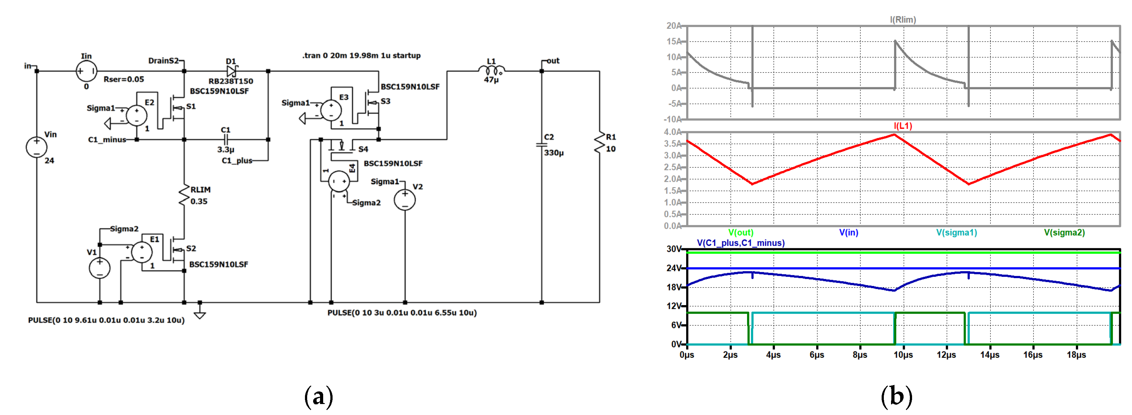
Figure 25.
KY Buck-Boost converter type I with reduced limiting resistor: (a) simulation circuit; (b) up to down: current through the limiting resistor RLIM (grey); current through L1 (red); output voltage (green), input voltage (blue), voltage across C1 (dark blue), control signal of S1 (turquoise), control signal of S2 (dark green).
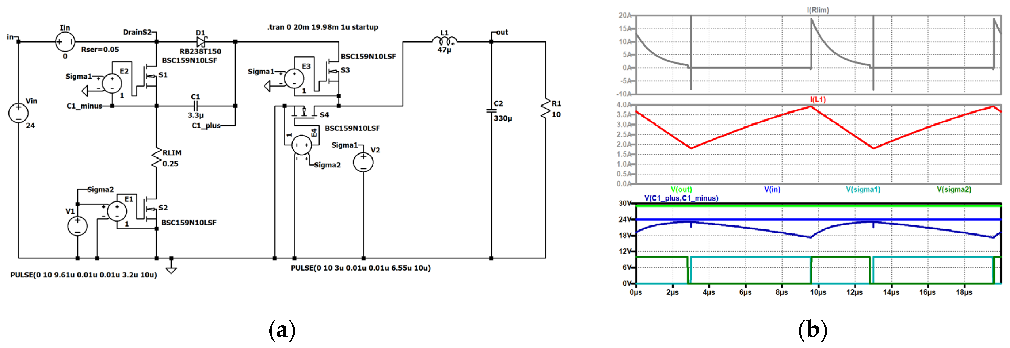
Figure 26.
KY Buck-Boost converter type II with limiting resistor.
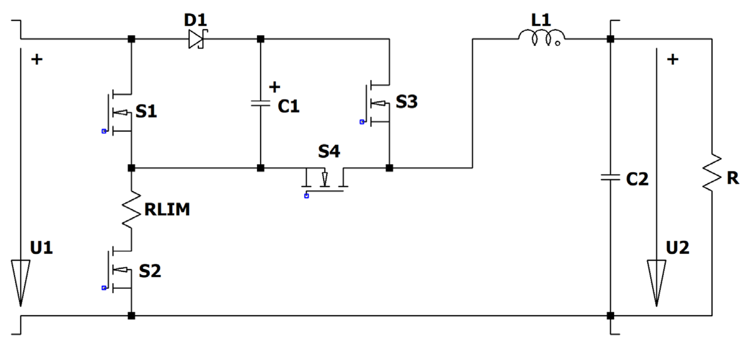
Figure 27.
KY Buck-Boost converter type II with limiting resistor: (a) simulation circuit; (b) up to down: current through the limiting resistor RLIM (grey); current through L1 (red); output voltage (green), input voltage (blue), voltage across C1 (dark blue), control signal of S1 (turquoise), control signal of S2 (dark green).
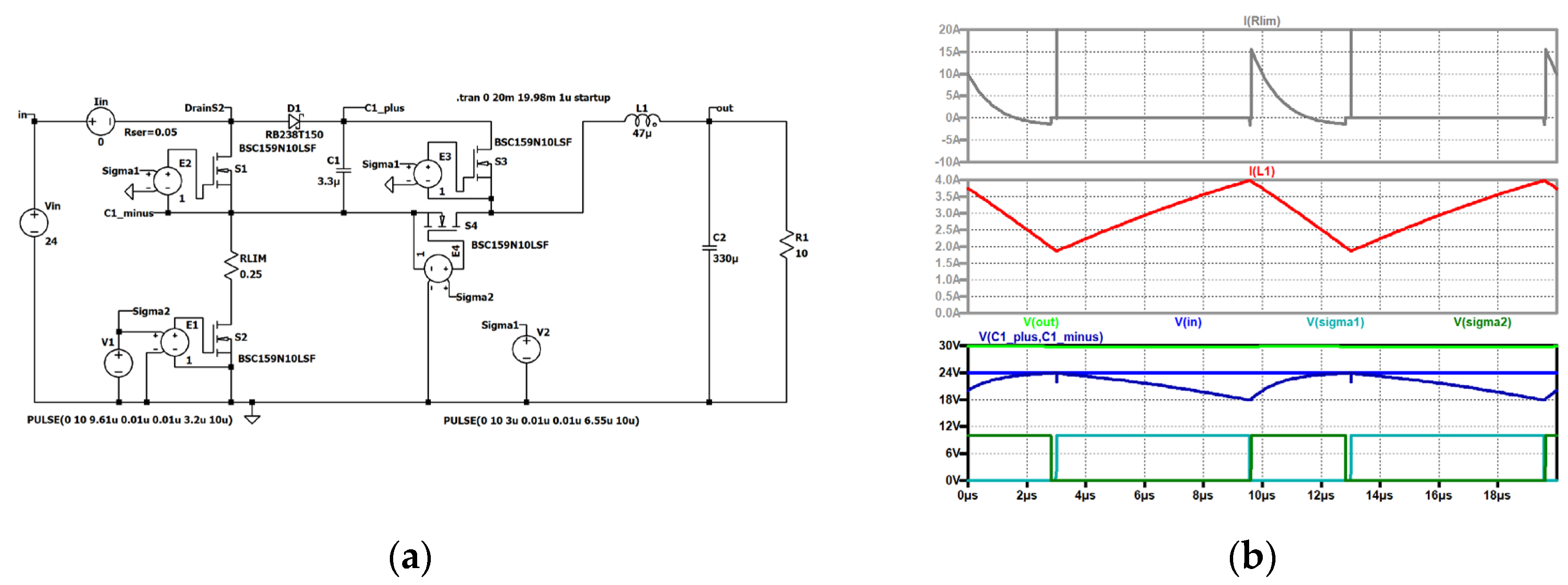
Figure 28.
Improved KY converter: (a) coil in series to the input; (b) coil in series to S2.
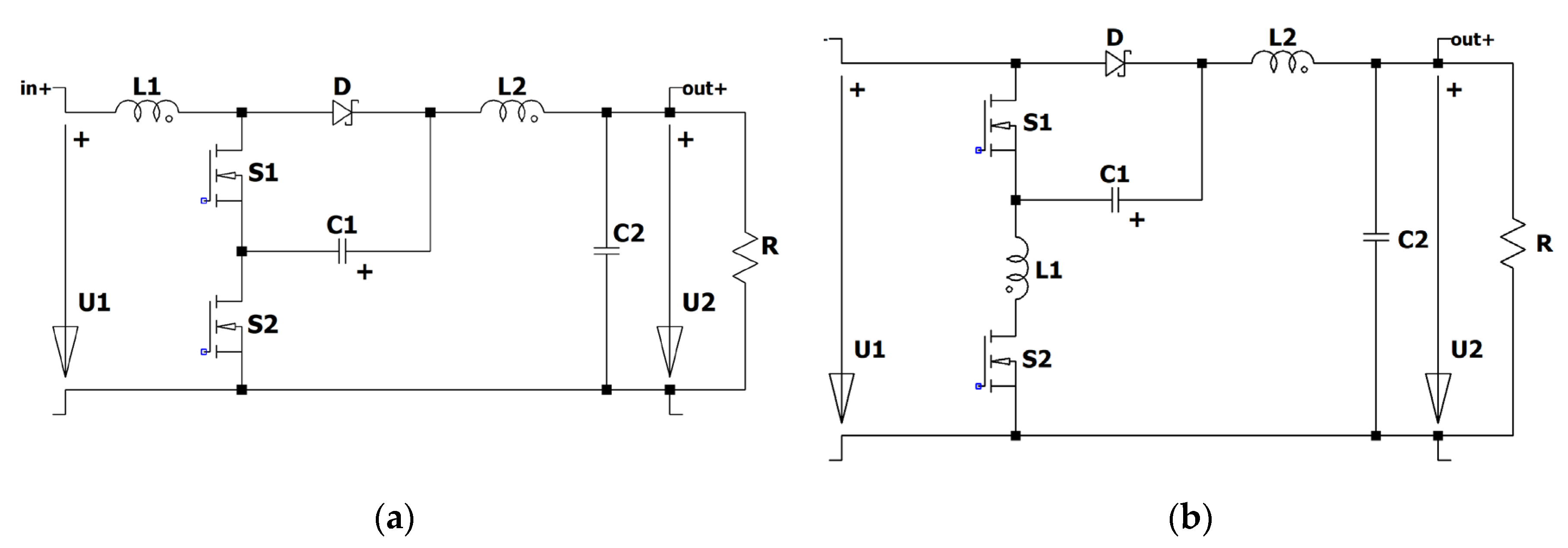
Figure 29.
Improved KY converter: (a) simulation circuit; (b) top to bottom: input current (violet), current through the second switch (grey); current through the coil (red); output voltage (green), voltage across the intermediate capacitor (dark blue), input voltage (blue), control signal of switch S2 (dark green, shifted), control signal of switch S1 (turquoise).
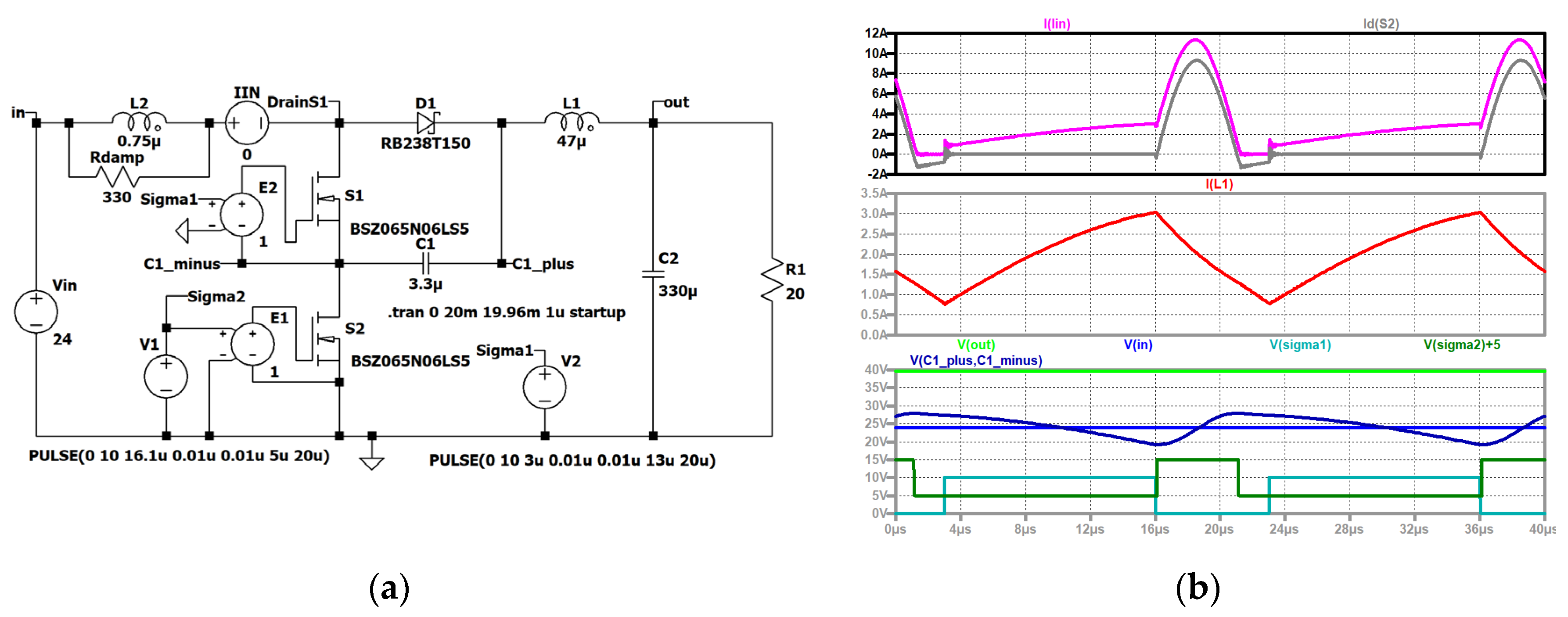
Figure 30.
Improved negative output KY Boost converter.
Figure 31.
Improved negative output KY Boost converter: (a) simulation circuit; (b) top to bottom: current through the active switch which is equal to the input current (grey); current through the coil (red); voltage across the intermediate capacitor (dark blue), input voltage (blue), control signal of switch S1 (turquoise), output voltage (green). A detailed explanation can be found in [11].
Figure 32.
Improved negative output KY Boost converter type II.
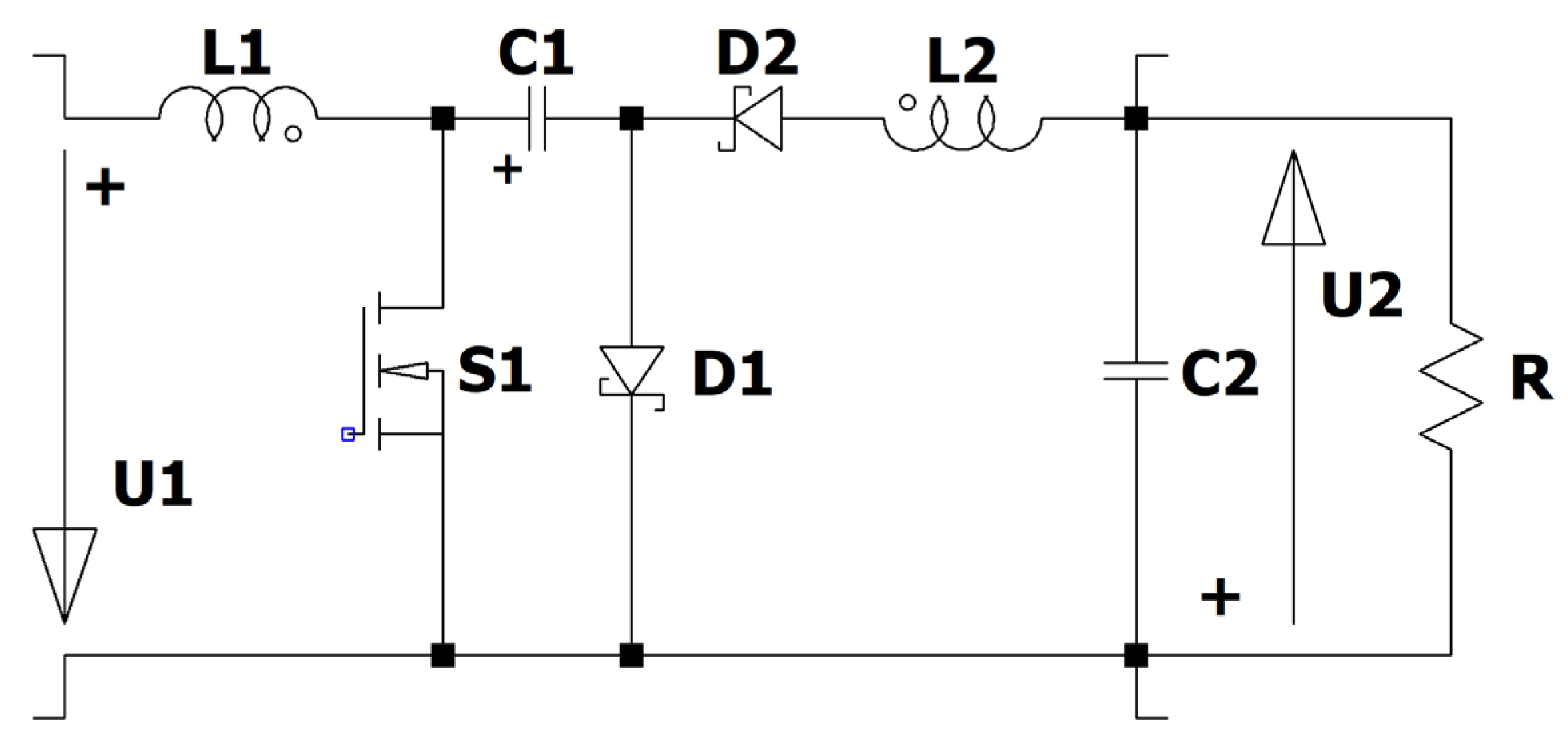
Figure 33.
Improved negative output KY Boost converter type II: (a) simulation circuit; (b) top to bottom: current through the intermediate capacitor C1 (dark green); current through the first diode (grey), current through the resonant coil L2 (violet); current through the main coil L1 (red); input voltage (blue), control signal of switch S1 (turquoise), voltage across the intermediate capacitor (dark blue), output voltage (green).
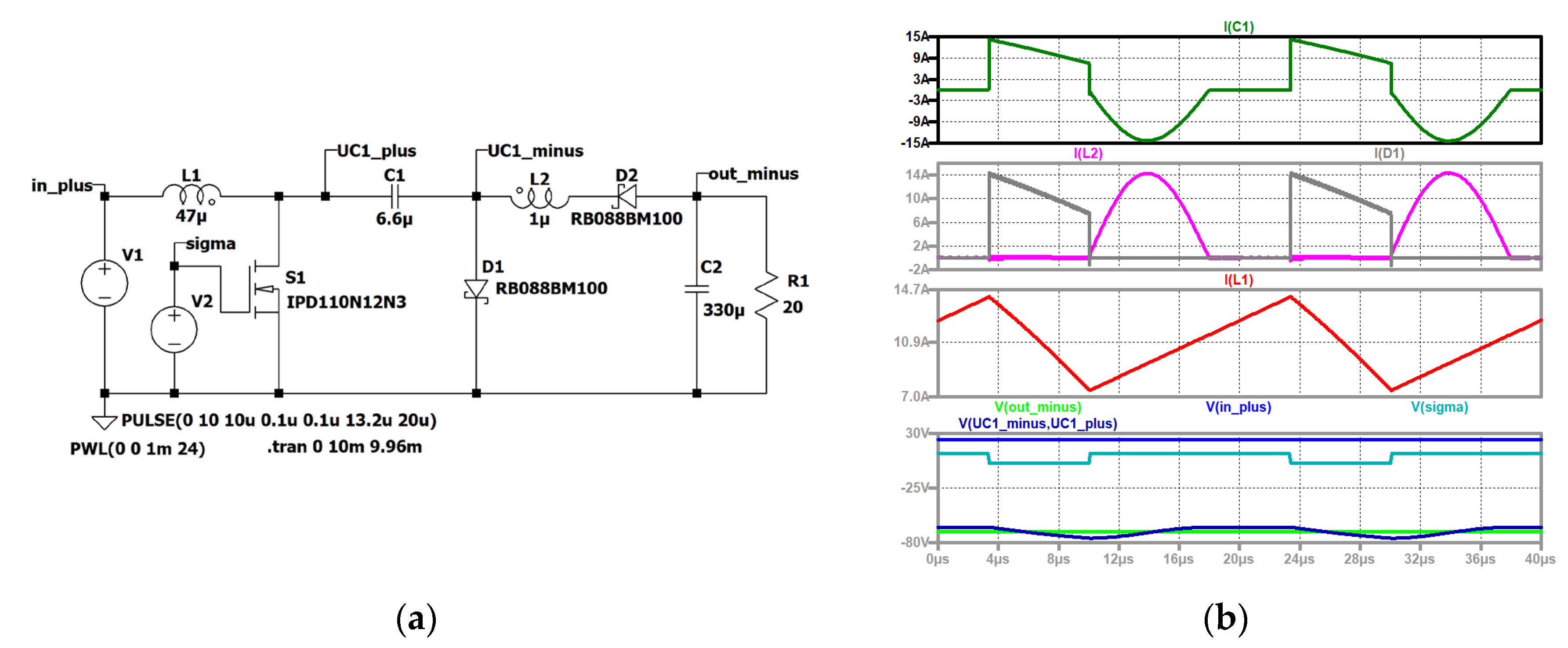
Figure 34.
Improved negative output KY Buck-Boost converter.
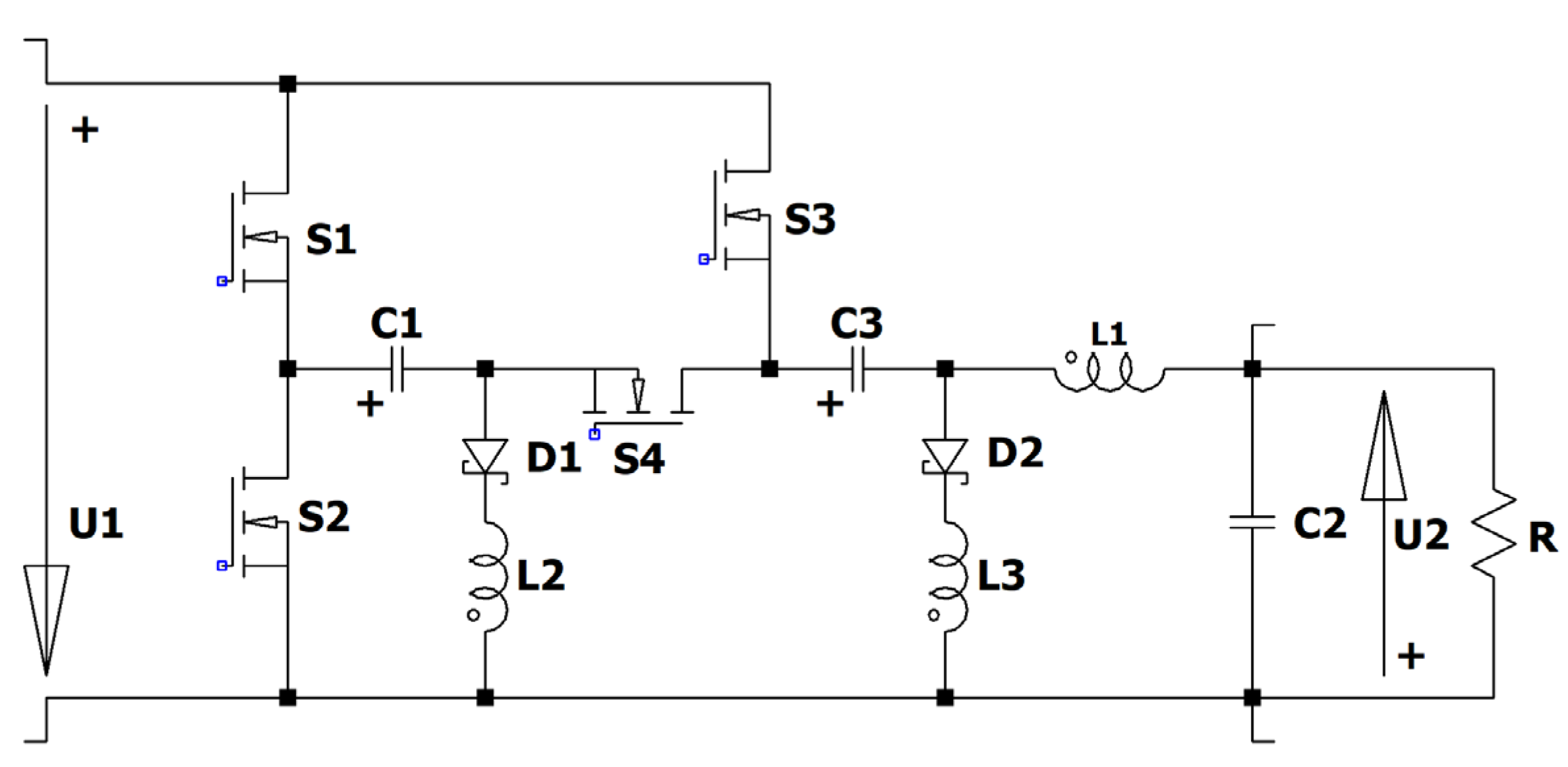
Figure 35.
Improved negative output KY Buck-Boost converter: (a) simulation circuit; (b) top to bottom: input current (violet), current through the diode D1 (grey); current through the main coil L1 (red); voltage across the intermediate capacitor (dark blue), input voltage (blue), control signal of the switches S2 and S4 (dark green, shifted), control signal of the switches S1 and S3 (turquoise), output voltage (green).
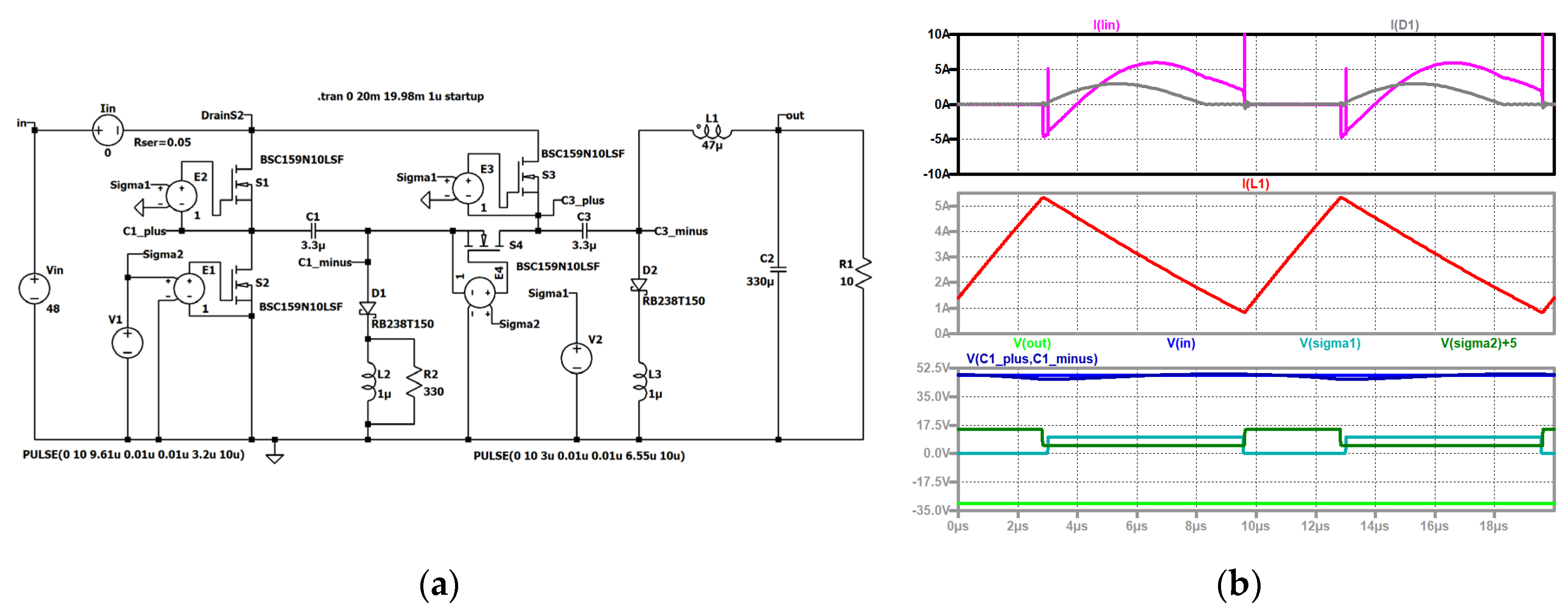
Figure 36.
Improved KY Buck-Boost converter type I.
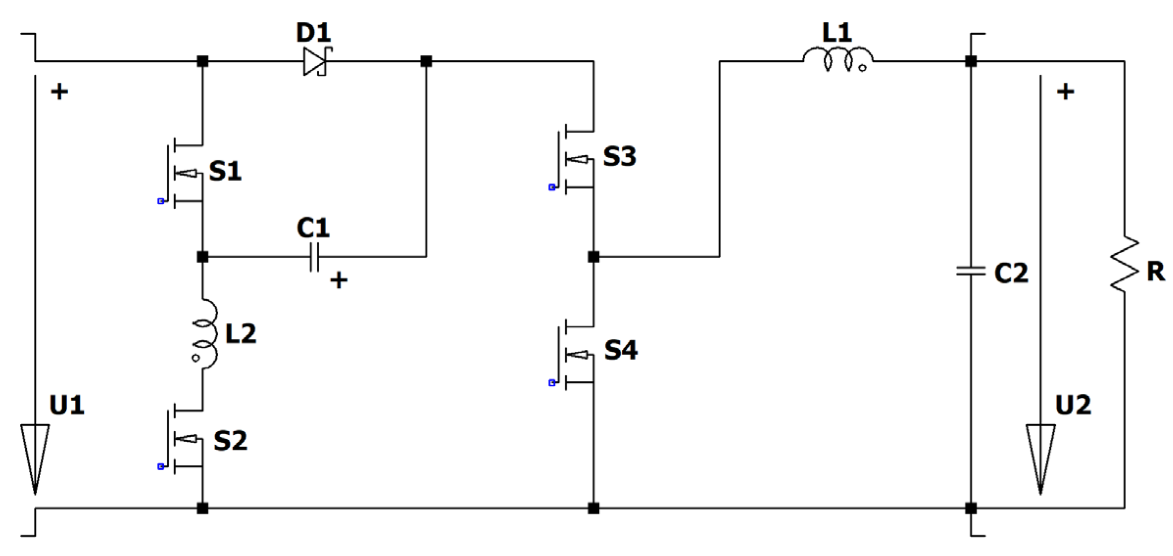
Figure 37.
Improved KY Buck-Boost converter type I: (a) simulation circuit; (b) top to bottom: input current (violet); current through the main coil L1 (red); output voltage (green), voltage across the intermediate capacitor (dark blue), input voltage (blue), control signal of the switches S2 and S4 (dark green), control signal of the switches S1 and S3 (turquoise).
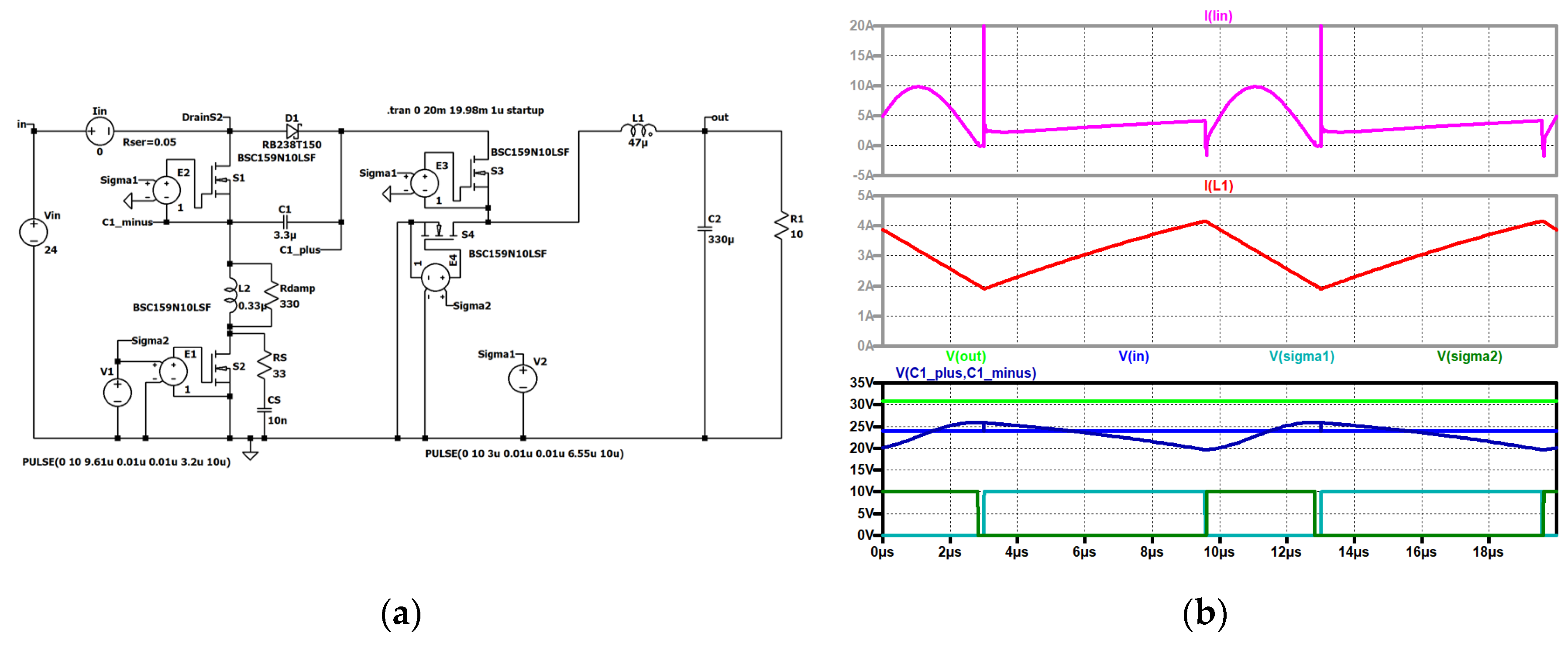
Figure 38.
Improved KY Buck-Boost converter type II.
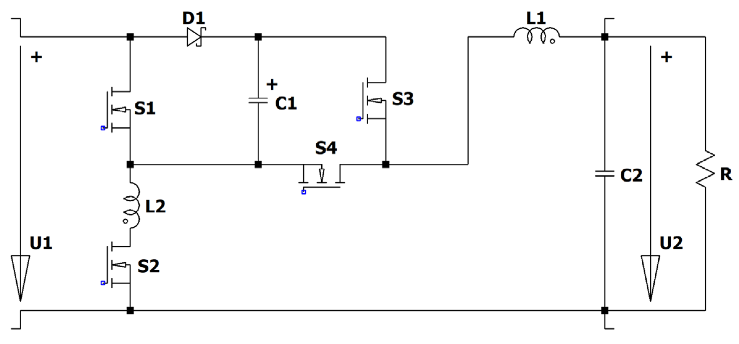
Figure 39.
Improved KY Buck-Boost converter type II: (a) simulation circuit; (b) top to bottom: input current (violet); current through the main coil L1 (red); output voltage (green), voltage across the intermediate capacitor (dark blue), input voltage (blue), control signal of the switches S2 and S4 (dark green, shifted), control signal of the switches S1 and S3 (turquoise).
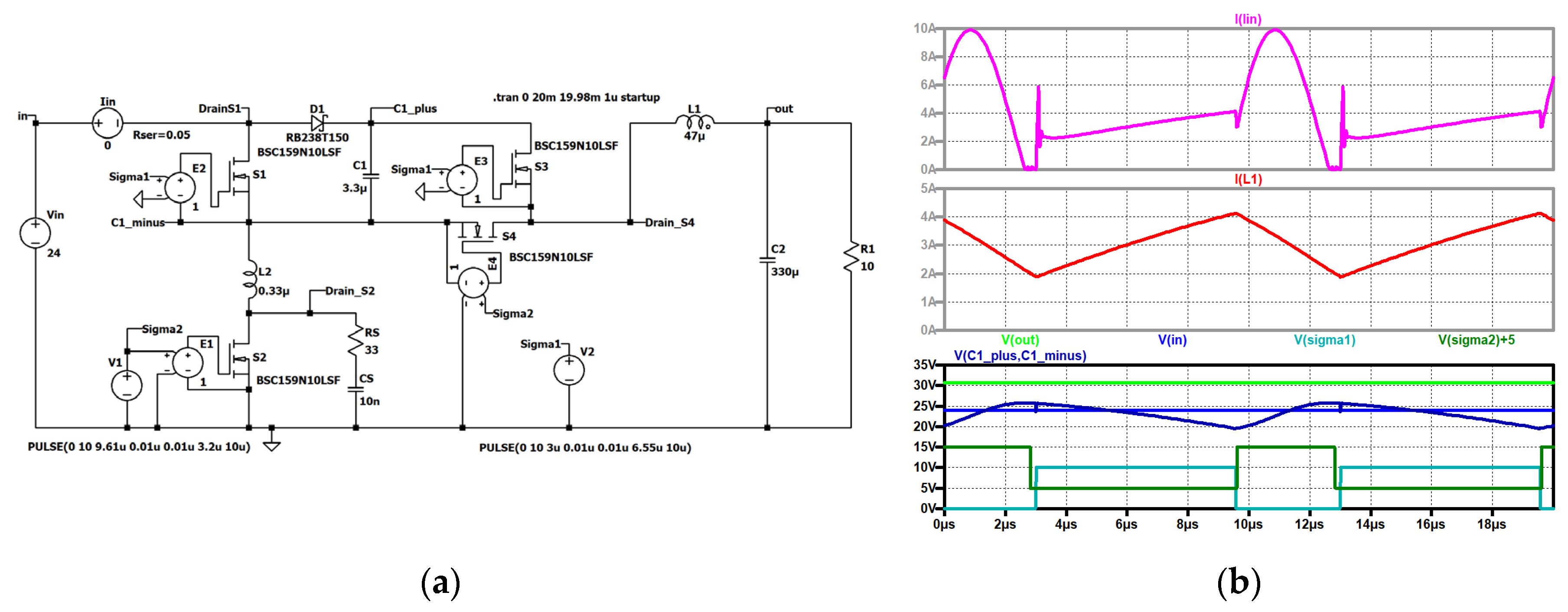

Table 1.
Possible positions of the limiting resistor.
| In series to C1 | Leads to additional losses during M1 |
| In series to S2 | Losses only by the charging current |
| In series to D | Additional losses during M2 |
| In front of the circuit | Always additional losses |
Disclaimer/Publisher’s Note: The statements, opinions and data contained in all publications are solely those of the individual author(s) and contributor(s) and not of MDPI and/or the editor(s). MDPI and/or the editor(s) disclaim responsibility for any injury to people or property resulting from any ideas, methods, instructions or products referred to in the content. |
© 2025 by the authors. Licensee MDPI, Basel, Switzerland. This article is an open access article distributed under the terms and conditions of the Creative Commons Attribution (CC BY) license (https://creativecommons.org/licenses/by/4.0/).
Copyright: This open access article is published under a Creative Commons CC BY 4.0 license, which permit the free download, distribution, and reuse, provided that the author and preprint are cited in any reuse.


