
Submitted:
21 May 2025
Posted:
22 May 2025
You are already at the latest version
Abstract
This paper focuses on the development of a high-conversion-efficiency DC/DC boost converter, which features high step-up conversion and employs soft switching technology to reduce con-version losses. In the proposed design, the conventional energy storage inductor used in tradi-tional boost converters is replaced with a coupled inductor, and an additional boost circuit is in-troduced. This configuration allows the converter to achieve a higher voltage conversion ratio under the same duty cycle, thereby enhancing the voltage gain of the converter. Additionally, a resonance branch is incorporated into the converter, and by applying a simple switching signal control, zero voltage switching (ZVS) of the main switch is realized. This reduces the switching loss inherent in hard switching high step-up converters, thereby improving the overall conver-sion efficiency. To validate the performance of the proposed converter, the circuit principle of the proposed high step-up soft switching converter is first analyzed, followed by the design of the circuit components. Subsequently, the feasibility of the proposed converter is verified using PSIM simulation software. Finally, the proposed high step-up soft switching boost converter is tested using the TMS320F2809 digital signal processor, and it is verified that the main switch successfully achieves ZVS. The converter operates under a full load of 340W, achieving a conver-sion efficiency of 92.7%, demonstrating the excellent conversion performance of the developed converter.
Keywords:
high step-up converter
; soft switching converter
; zero voltage switching
; coupled inductor
; switching loss
1. Introduction
In recent years, renewable energy has gained increasing attention, with photovoltaic power generation system becoming one of the most widely applied forms of renewable energy. These systems are characterized by sustainable energy supply and minimal environmental impact. With advancements in technology, the installation and operational costs of photovoltaic power generation systems have continuously decreased, and their long-term maintenance costs are also relatively low, making them an ideal energy supply option. Additionally, with the rapid development of power electronics technology, converters play a crucial role in photovoltaic power generation systems, as they can significantly improve the energy conversion efficiency of the system. The primary function of a converter is to convert the direct current (DC) generated by the photovoltaic module array into alternating current (AC) or other DC values, for use in the power grid or energy storage. Due to the relatively low voltage output of photovoltaic modules and the need for subsequent applications in high-voltage systems, boost converters [1,2,3] are commonly used in photovoltaic power generation systems. However, boost converters also have certain drawbacks. When the switch is operated within a reasonable duty cycle, in order to prevent overheating and damage to the switch during prolonged operation, the voltage gain of the converter is limited, thus failing to meet the requirement for high output voltage. Moreover, if the switching frequency is too high when operating the switch, it results in significant switching losses. Although soft switching technologies [4,5,6,7] can reduce switching losses, they increase the size and cost of the converter and still cannot achieve the required higher output voltage. These issues affect the overall performance and cost-effectiveness of the photovoltaic power generation system.
In recent years, many researchers have begun to explore high step-up converters [8,9,10,11] to address the drawbacks of traditional boost converters. High step-up converters can convert the relatively low output voltage from a photovoltaic module array to a higher voltage, thereby reducing energy losses and improving system efficiency. However, this technology also faces several challenges. The design of high step-up converters is more complex and requires advanced electronic components and control techniques, which leads to increased manufacturing costs and greater risks to system reliability. Additionally, high step-up converters operate in high-voltage environments, posing potential voltage breakdown and insulation issues. Therefore, special insulation designs and protection measures are necessary. The boost converter presented in reference [8] demonstrates excellent step-up performance. However, due to the use of a three-winding coupled inductor, which increases the voltage gain through the turns ratio, the converter's physical size becomes significantly larger. In addition, the main switch in this converter does not achieve soft switching, resulting in higher switching losses during transitions between the on and off states. Furthermore, as the output voltage increases, the main switch must withstand higher voltage and current levels, significantly reducing the switch's lifespan. Reference [9] proposes a multi-stage series connection to increase the voltage gain; but the conversion efficiency decreases as the number of stages increases. Reference [10] presents an inductively coupled soft switching bidirectional converter, which offers a high step-up ratio and reduces input voltage ripple. However, it requires five switch components and six capacitors, which increases the size and cost of the physical hardware. Reference [11] introduces an interleaved high voltage ratio boost converter with coupled inductor. However, during the interleaved operation, the inactive converter still transmits some power, which reduces the overall efficiency and causes distortion in the average current. Reference [12] proposed an inductively coupled soft-switching bidirectional converter that also achieves a high step-up ratio. However, its main switch components must withstand higher voltage switching stresses, requiring switches with higher voltage ratings.
To address the drawbacks of the aforementioned converters, this paper proposes a high step-up soft switching converter. This converter uses a coupled inductor to replace the conventional energy storage inductor and incorporates a boost circuit, enabling a higher voltage conversion ratio under the same duty cycle, thereby improving the voltage gain of the converter. In addition, this paper incorporates a resonance branch into the converter and uses a simple switch signal control to achieve ZVS of the main switch, reducing switching losses in hard switching high step-up converters and improving conversion efficiency. First, the circuit architecture of the proposed converter was established using PSIM simulation software [13], and its feasibility was verified through simulation analysis. Finally, the implementation was carried out using the TMS320F2809 digital signal processor [14] from Texas Instruments, which demonstrated the superior conversion performance of the high step-up soft-switching converter.
2. The Proposed High Step-Up Converter
2.1. Operating Principle of the High Step-Up Hard Switching Converter
Figure 1 depicts the circuit architecture of the proposed high step-up hard-switching converter. This design replaces the traditional energy storage inductor with a coupled inductor and incorporates an additional boost circuit formed by and . By leveraging the turns ratio of the coupled inductor and the boost circuit, the voltage conversion ratio is significantly enhanced. Furthermore, the converter features a simple circuit structure and ease of control, making it advantageous for practical applications. The operation of the converter can be divided into two modes based on the state of the switch (on and off). When the switch is on, the duty cycle of the converter during one period T is defined by Equation (1).
Where is the time during which the switch is conducting within one period, and is the time during which the switch is off.
- (1)
- Switch on ()
When the switch S is conducting, the diode is also conducting, while the diode and are in the off state. The equivalent circuit is shown in Figure 2, and the turns ratio N of the coupled inductor is defined by Equation (2). At this point, the inductor voltages and are expressed by Equations (3) and (4), respectively, while the voltage across the energy storage capacitor , is given by Equation (5).
- (2)
- Switchoff ()
When the switch S is off, diode is in the off state, while diodes and are conducting. The equivalent circuit is shown in Figure 3, and the inductor voltages and are given by Equations (6) and (7), respectively.
Based on the volt-second balance theorem for the inductor , the Equations (4) and (7) lead to Equation (8). After simplification, the voltage conversion ratio between the output voltage and the input voltage can be expressed by Equation (9).
From Equation (9), the relationship between the voltage gain of the converter and the duty cycle is shown in Table 1. From Table 1 and Figure 4, it can be observed that, for the same duty cycle, the voltage conversion ratio of the converter can be increased by adjusting the turns ratio of the coupled inductor.
2.2. Operating Principle of the High Step-Up Hard Switching Converter
The high step-up hard switching converter described above can increase the converter’s voltage conversion ratio by utilizing a coupled inductor and an additional boost circuit. However, if the voltage or current cannot be reduced to zero before switching occurs, switching losses will arise, which in turn lowers the overall efficiency of the converter. To improve the conversion efficiency, this paper proposes a high step-up soft switching converter with an inductive coupling. The circuit architecture of this converter is shown in Figure 5, while Figure 6 illustrates the switching control signals for the converter [15]. The converter achieves a high voltage conversion ratio through inductive coupling and an additional boost circuit. It also incorporates a resonant branch composed of , and , where is the capacitor originally used in the hard switching converter circuit. By controlling the switching signals, the converter enables ZVS for the main switch, thus improving efficiency and reducing switching losses. This paper will analyze the operating modes of the proposed soft switching converter, which is divided into nine distinct modes. Figure 7 shows the switching waveforms for each component. Before explaining the operating modes, the following assumptions are made:
1) The converter operates in continuous conduction mode (CCM), and the circuit has reached a steady state.
2) All components are ideal, meaning that during conduction they are treated as short circuits, and during cutoff, as open circuits. Consequently, there is no conduction voltage drop across the power switching components.
3) The input and output voltages are maintained at constant values.
4) The currents of the energy storage inductors and are considered constant (i.e. , ).
- (1)
- Mode 1()
When operating in Mode 1, the equivalent circuit is shown in Figure 8. In this mode, the main switch S is in the off state, while the auxiliary switch Sr is turned on first. As a result, the resonant capacitor begins to discharge, and the voltage across the resonant inductor is . The current through the resonant inductor rises from zero. Therefore, the resonant inductor and resonant capacitor form a resonant tank, and the circuit equations can be expressed by Equation (10). After solving, the and are given by Equation (11), while the resonant impedance and resonant angular frequency are given by Equation (12). When the voltage across the resonant capacitor drops to , diode switches from the off state to the on state. The circuit then transitions to Mode 2. The time for this transition is given by Equation (13).
Where the resonance impedance and resonance frequency
- (2)
- Mode2 ()
When entering working Mode 2, the equivalent circuit is shown in Figure 9. At this point, the voltage across the resonant capacitor has decreased to . At this point, the auxiliary switch Sr remains on, and both the resonant inductor and the resonant capacitor continue to form a resonant circuit. The resonant inductor current will continue to increase, and the resonant capacitor will keep discharging. The circuit equations for this mode can be expressed as Equation (14). From Equation (14), and can be derived as shown in Equation (15). When the voltage across the resonant capacitor drops to zero, at which point , the resonant inductor current can be calculated from Equation (15) as shown in Equation (16). The operating time for this mode can be derived as shown in Equation (17). At this point, the anti-parallel diode of the main switch S will begin to conduct, and the system will enter working Mode 3.
- (3)
- Mode 3 ()
When the system enters working Mode 3, the equivalent circuit is shown in Figure 10. At this point, the voltage across the resonant capacitor has dropped to a very small negative voltage, which causes the anti-parallel diode of the main switch S to forward conduct. As a result, the voltage across the main switch S is zero. The control of the main switch S is then switched from the off state to the on state, achieving ZVS for the main switch S. At the same time, the auxiliary switch Sr is switched off. The circuit equations for this mode can be expressed as Equation (18). To ensure ZVS for the main switch, the delay time must satisfy the condition in Equation (19), and typically is 5% to 10% of the switching period T. Moreover, to ensure that the main switch S can still achieve ZVS under heavy load conditions, and considering the turn-off speed of the auxiliary switch Sr, an additional time delay must be considered. Thus, the operating time of the auxiliary switch can be expressed as shown in Equation (20).
- (4)
- Mode4 ()
In Mode 4, the main switch S is conducting, while the auxiliary switch Sr switches off. Diodes and are forward-biased, and the equivalent circuit is shown in Figure 11. In this mode, to allow the energy storage capacitor and the resonant inductor to form a resonant tank, the capacitance of is chosen to be close to that of . Additionally, the resonant inductor and the common-mode inductance both discharge into the energy storage capacitor. At this point, the current through the resonant inductor is . The circuit equation for this mode can be expressed as Equation (21). Solving for and gives Equation (22). In this working mode, the current through the resonant inductor decreases from to zero, and diodes and switch off. The circuit then transitions into Mode 5.
- (5)
- Mode5 ()
In Mode 5, the equivalent circuit is shown in Figure 12. At this point, the main switch S remains conducting. The circuit equation for this mode can be expressed as Equation (23). This mode continues until the main switch S transitions from conducting to off.
- (6)
- Mode6 ()
In Mode 6, the main switch S is turned off and the equivalent circuit is shown in Figure 13. As a result, the current charges the resonant capacitor , causing the voltage across the resonant capacitor to gradually increase. The circuit equation for this mode is given by Equation (24). By solving Equation (24), can be obtained as Equation (25). When the resonant capacitor voltage reaches , this mode ends and transitions into Mode 7. Therefore, the operating time for this mode can be determined from Equation (26).
- (7)
- Mode7 ()
In Mode 7, the voltage across the resonant capacitor is , and the main switch S remains in the off state, while the auxiliary switch Sr is also off. As a result, the coupled inductor and the energy storage capacitor transfer energy to the load via diode D. The circuit equation for this mode is given by Equation (27), and the equivalent circuit is shown in Figure 14. By solving Equation (27), the voltage across the resonant capacitor can be obtained as Equation (28). At this point, the current flowing through the coupled inductor and the current gradually decrease, and when the currents and become equal, the circuit transitions into Mode 8.
- (8)
- Mode8 ()
In Mode 8, the voltage across the resonant capacitor is , and diode transitions from the conducting to the off state. The resonant capacitor stops charging, and both the main switch S and the auxiliary switch Sr remain off. Consequently, the coupled inductor and the energy storage capacitor continue to transfer energy to the load. The equivalent circuit for this mode is shown in Figure 15, and the circuit equation is given by Equation (29). When the voltage across the energy storage capacitor drops to zero, this mode ends, and the circuit transitions into Mode 9.
- (9)
- Mode9 ()
In Mode 9, the voltage across the energy storage capacitor is zero, and diode D transitions from conducting to the off state. Both the main switch S and the auxiliary switch Sr remain off. The equivalent circuit for this mode is shown in Figure 16, marking the completion of the entire switching cycle analysis. The cycle will repeat once the auxiliary switch Sr turns on again, returning to Mode 1 of the next cycle.
To demonstrate the performance of the proposed high step-up soft switching converter, a comparison is made with various high step-up soft switching converters. The comparison is based on voltage gain, switch voltage ratings, number of switching components, number of diode components, number of inductive components, and number of capacitive components. The results are summarized in Table 2. As shown in the table, the proposed converter achieves a high voltage gain with fewer components and utilizes simple signal control for soft switching, highlighting its key advantages.
3. Component Design of the Proposed High Step-Up Converter
The output power of the high step-up hard switching converter proposed in this paper is 340W. The relevant circuit parameters and specifications are provided in Table 3.
In the case where all components are operating under ideal conditions, the input power should be equal to the output power, i.e.
Substituting Equation (9) into Equation (31) yields, as expressed in Equation (32).
where represents the voltage gain of the converter.
When the main switch S is turned on, can be expressed as:
From Equation (33), it can be observed that when the main switch is turned on, the inductor current increases linearly, with the conduction time denoted as . The rate of change of the inductor current can be calculated as shown in Equation (34).
Using Equations (32) and (34), the maximum and minimum values of the inductor current can be derived, as expressed in Equations (35) and (36) [16].
If , the inductor can operate at the boundary between CCM and discontinuous conduction mode, which yields:
From Equation (37), the value of can be calculated as:
Since the coupled inductor structure is similar to the coupled transformer structure, the maximum value of can be shown as [16]:
3.1. Design of Coupled Inductors
The given scenario involves ensuring that a converter operates in CCM across all duty cycles, with a maximum output power of 340W, a fixed output voltage of 430V, and a rated load of 550Ω. From the relationship between the duty cycle D and the function curve shown in Figure 17, it is observed that the function reaches its maximum value when D=0.33. By substituting the load resistance R=550Ω, the turns ratio of the coupled inductors N=2, the switching frequency f=25kHz, and the duty cycle D=0.33 into Equation (38), the minimum primary inductance of the coupled inductor is calculated to be 102μH. To ensure that the coupling inductor operates in CCM under both light and heavy load conditions, the calculated inductance value is further multiplied by a safety factor of 1.25. Hence, the selected value of the coupling inductor is 127 μH.
3.2. Design of Capacitors and
From Figure 1 of the high step-up hard switching converter, it can be observed that the capacitor , coupled inductor , main switch S, and diode form a traditional boost converter. When the duty cycle of the main switch S is 0.8, the voltage across capacitor is approximately 360V. From Equation (5), under the same operating conditions, the voltage across capacitor is around 500V. Therefore, the rated voltage of capacitor is selected as 400V, while the rated voltage of capacitor is 600V. Based on the analysis of operating Mode 3 in Equation (18) and Figure 7, it is evident that the capacitance value of influences the reverse current flowing through the main switch S. Considering ripple size and component availability, the chosen capacitance value for is 0.33μF/400V. Additionally, from the explanation of operating Mode 4 of this high step-up soft-switching converter, it is understood that should have a capacitance value similar to that of , so is selected as 0.33μF/600V.
3.3. Design of Resonant Inductor
Since the conduction time of the auxiliary switch in a typical soft switching converter is usually designed to be between 5% and 10% of the switching period, let () and represent these values, respectively. From Equation (20), if the duty cycle D is set within the range of 0.1 to 0.8, the resonance inductance value can be calculated to vary between 8.08μH and 17.08μH. Based on this, the chosen resonance inductance for the converter is 18μH.
After the design of the aforementioned components, the specifications of the components used in the proposed high step-up soft-switching converter are listed in Table 4.
4. Simulation Results
The PSIM simulation software [13] was first used in this study to model the high step-up soft switching converter, in order to verify that the proposed converter achieves superior conversion performance under both light and full load conditions. Figure 18 shows the waveform of the duty cycle, input voltage, and output voltage when the converter operates at full load (P=340W). The output voltage of 430V is obtained when the input voltage is 72V and the duty cycle is 0.33, as shown in Figure 18. Therefore, the converter exhibits a high step-up ratio, and its voltage gain is consistent with the value listed in Table 1. Figure 19 and Figure 20 show the simulation waveforms of the electrical quantities for the main switch S and auxiliary switch Sr when the converter operates at full load (P=340W). Figure 21 and Figure 22 show the simulation waveforms of the electrical quantities for the main switch S and auxiliary switch Sr when the converter operates at light load (P=100W). From Figure 19 and Figure 21, it can be observed that at both full load (P=340W) and light load (P=100W), the voltage across the main switch S drops to zero before the switch enters the conduction mode. This demonstrates that the main switch S achieves ZVS, confirming that the proposed converter enables soft-switching for the main switch.
5. Experimental Results
After verifying the feasibility of the proposed converter using PSIM simulation software, the practical implementation of the high step-up soft switching converter was conducted using the TMS320F2809 [14] digital signal processor as the control core. The overall hardware circuit setup is shown in Figure 23, and the test platform is depicted in Figure 24. Figure 25 shows the waveforms of the trigger signal for the main switch S, input voltage, and output voltage of the high step-up soft-switching converter under full-load operation P=340W. From Figure 25, it can be observed that when the duty cycle of the main switch is 0.33 and the input voltage is 72V, the output voltage reaches 430V, achieving the expected voltage gain as shown in Table 1. Figure 26, Figure 27, Figure 28 and Figure 29 show the waveforms of the trigger signals, voltages, and currents for the main switch S and auxiliary switch Sr at load conditions of P=100W and P=340W, respectively. The experimental results demonstrate that the proposed high step-up ratio soft switching converter achieves ZVS for the main switch S under both light load (P=100W) and full load (P=340W) conditions. This helps reduce the switching loss, thereby improving the overall conversion efficiency. Additionally, the measured waveforms of the main switch S and auxiliary switch Sr match the simulated waveforms. Figure 30 shows a comparison of the efficiency between the proposed high step-up soft-switching and hard-switching converters, with loads ranging from P=100W to P=340W. The figure demonstrates that the conversion efficiency improves by 3-4% across different load levels.
6. Conclusion
This paper presents a high step-up soft switching converter topology. Through both simulation analysis and experimental results, it has been demonstrated that the converter achieves zero voltage switching (ZVS) for the main switch. By replacing the traditional energy storage inductor with a coupled inductor and adding a boost circuit, the overall voltage gain of the converter is enhanced, enabling it to achieve a higher voltage output. Additionally, a resonant branch is incorporated to ensure the main switch operates with ZVS, thereby reducing switching losses and switch stress, which in turn improves conversion efficiency. The proposed converter offers advantages such as ease of control via triggering signals, a simple circuit topology, and quantifiable component design parameters. Under different load conditions, the conversion efficiency improves by 3-4%, with a peak efficiency of approximately 93%. Thus, the converter demonstrates excellent conversion performance. This converter is promising for practical applications in photovoltaic module arrays, where it can be used for maximum power point tracking to enhance power generation efficiency.
Author Contributions
K.-H.C. managed the project and completed the soft-switching of the DC-DC converter. K.-H.C. also planned the project and wrote, edited and reviewed the manuscript. T.T.T.B. completed the formal analysis of the high step-up ratio DC-DC converter. T.T.T.B. was also responsible for the software program and validation of the experimental results. All authors have read and agreed to the published version of the manuscript.
Funding
The authors gratefully acknowledge the support and funding of this project by National Science and Technology Council, Taiwan, under the Grant Number NSTC 113-2221-E-167-035.
Institutional Review Board Statement
Not applicable.
Informed Consent Statement
Not applicable.
Data Availability Statement
This study did not report any data.
Conflicts of Interest
The authors of the manuscript declare no conflicts of interest.
Nomenclature
| Acronyms | |
| ZVS | zero voltage switching |
| DC | direct current |
| AC | alternating current |
| CCM | continuous conduction mode |
| Symbols | |
| the input voltage | |
| the output voltage | |
| the input power | |
| the output power | |
| duty cycle between [0;1] | |
| the switching period of converter | |
| the switch conduction time within one cycle | |
| the switch off time within one cycle | |
| delay time | |
| an additional time delay | |
| the operating time of the auxiliary switch | |
| turns ratio of coupling inductor | |
| , | the number of turns in the first and second coils |
| the conversion ratio of the high voltage ratio soft switching converter | |
| switching frequency | |
| main switch | |
| the current through the main switch S | |
| the voltage across the main switch S | |
| auxiliary switch | |
| the current through the auxiliary switch Sr | |
| the voltage across the auxiliary switch Sr | |
| , | the primary side and secondary side of the coupled inductor |
| , | the current through the primary and secondary sides of the coupled inductor |
| , | the constant current through the primary and secondary sides of the coupled inductor |
| , | the voltage across the primary and secondary sides of the coupled inductor |
| resonant inductor | |
| the current through the resonant inductor Lr | |
| the voltage across the resonant inductor Lr | |
| ,, | fast diodes |
| ,, | the current through the fast diode,and |
| filter capacitor | |
| resonant capacitor | |
| the current through the resonant capacitor | |
| the voltage across the resonant capacitor | |
| energy storage capacitor | |
| the current through the energy storage capacitor | |
| the voltage across the energy storage capacitor | |
| output load | |
| resonance impedance | |
| resonance frequency |
References
- Hart, D.W. Introduction to Power Electronics, 2nd ed.; Pearson Educ. Taiwan Ltd.: Taipei, Taiwan, 2002; pp. 211–220. [Google Scholar]
- Park, D.; Lee, H. Improvements in Light-load Efficiency and Operation Frequency for Low-voltage Current-mode Integrated Boost Converters. IEEE Trans. Circuits Syst. II Exp. Briefs 2014, 61, 599–603. [Google Scholar] [CrossRef]
- Park, K.B.; Moon, G.W.; Youn, M.J. Overview of High-step-up Coupled-inductor Boost Converters. IEEE J. Emerg. Sel. Top. Power Electron. 2016, 4, 689–704. [Google Scholar]
- Sathyan, S.; Suryawanshi, H.M.; Ballal, M.S.; Shitole, A.B. Soft-switching DC–DC Converter for Distributed Energy Sources with High Step-up Voltage Capability. IEEE Trans. Ind. Electron. 2015, 62, 7039–7050. [Google Scholar] [CrossRef]
- Hassan, W.; Soon, J.L.; Lu, D.D.; Xiao, W. A High Conversion Ratio and High-efficiency Bidirectional DC–DC Converter with Reduced Voltage Stress. IEEE Trans. Power Electron. 2020, 35, 11827–11842. [Google Scholar] [CrossRef]
- Zheng, Y.; Brown, B.; Xie, W.; Li, S.; Smedley, K. High Step-up DC–DC Converter with Zero Voltage Switching and Low Input Current Ripple. IEEE Trans. Power Electron. 2020, 35, 9426–9429. [Google Scholar] [CrossRef]
- Chao, K.H.; Jheng, Y.C. A Soft-switching Coupled Inductor Bidirectional DC–DC Converter with High Conversion Ratio. Int. J. Electron. 2017, 105, 164–190. [Google Scholar] [CrossRef]
- Luo, P.; Liang, T.J.; Chen, K.H.; Chen, S.M. High Step-up DC–DC Converter with Active Switched Inductor and Voltage Doubler Based on Three-winding Coupled Inductor. In Proceedings of the IEEE Applied Power Electronics Conference and Exposition (APEC), Houston, TX, USA, 20–24 March 2022; pp. 731–736. [Google Scholar]
- Schmitz, L.; Martins, D.C.; Coelho, R.F. Generalized High Step-up DC–DC Boost-based Converter with Gain Cell. IEEE Trans. Circuits Syst. I Reg. Pap. 2017, 64, 480–493. [Google Scholar] [CrossRef]
- Santra, S.B.; Chatterjee, D.; Siwakoti, Y. Coupled Inductor Based Soft Switched High Gain Bidirectional DC–DC Converter with Reduced Input Current Ripple. IEEE Trans. Ind. Electron. 2023, 70, 1431–1443. [Google Scholar] [CrossRef]
- Yang, F.; Li, C.; Cao, Y.; Yao, K. Two-phase Interleaved Boost PFC Converter with Coupled Inductor under Single-phase Operation. IEEE Trans. Power Electron. 2020, 35, 169–184. [Google Scholar] [CrossRef]
- Sathyan, S.; Suryawanshi, H.M.; Ballal, M.S.; Shitole, A.B. Soft-switching DC–DC Converter for Distributed Energy Sources with High Step-up Voltage Capability. IEEE Trans. Ind. Electron. 2015, 62, 7039–7050. [Google Scholar] [CrossRef]
- Powersim. PSIM User Manual, Jan. 2023. Available online: https://powersimtech.com/wp-content/uploads/2021/01/PSIM-User-Manual.pdf (accessed on 30 April 2025).
- Texas Instruments. TMS320F2809 Datasheet, Sep. 2022. Available online: https://www.ti.com/lit/ds/symlink/tms320f2809.pdf (accessed on 30 April 2025).
- Chao, K.H.; Huang, B.Z.; Jian, J.J. An Energy Storage System Composed of Photovoltaic Arrays and Batteries with Uniform Charge/Discharge. Energies 2022, 15, 2883. [Google Scholar] [CrossRef]
- Narasimharaju, B.L.; Dubey, S.P.; Singh, S.P. Coupled Inductor Bidirectional DC–DC Converter for Improved Performance. In Proceedings of the International Conference on Industrial Electronics, Control and Robotics, Kakinada, India, 27–29 December 2010; pp. 1–5. [Google Scholar]
Figure 1.
Circuit diagram of the high step-up hard switching converter.
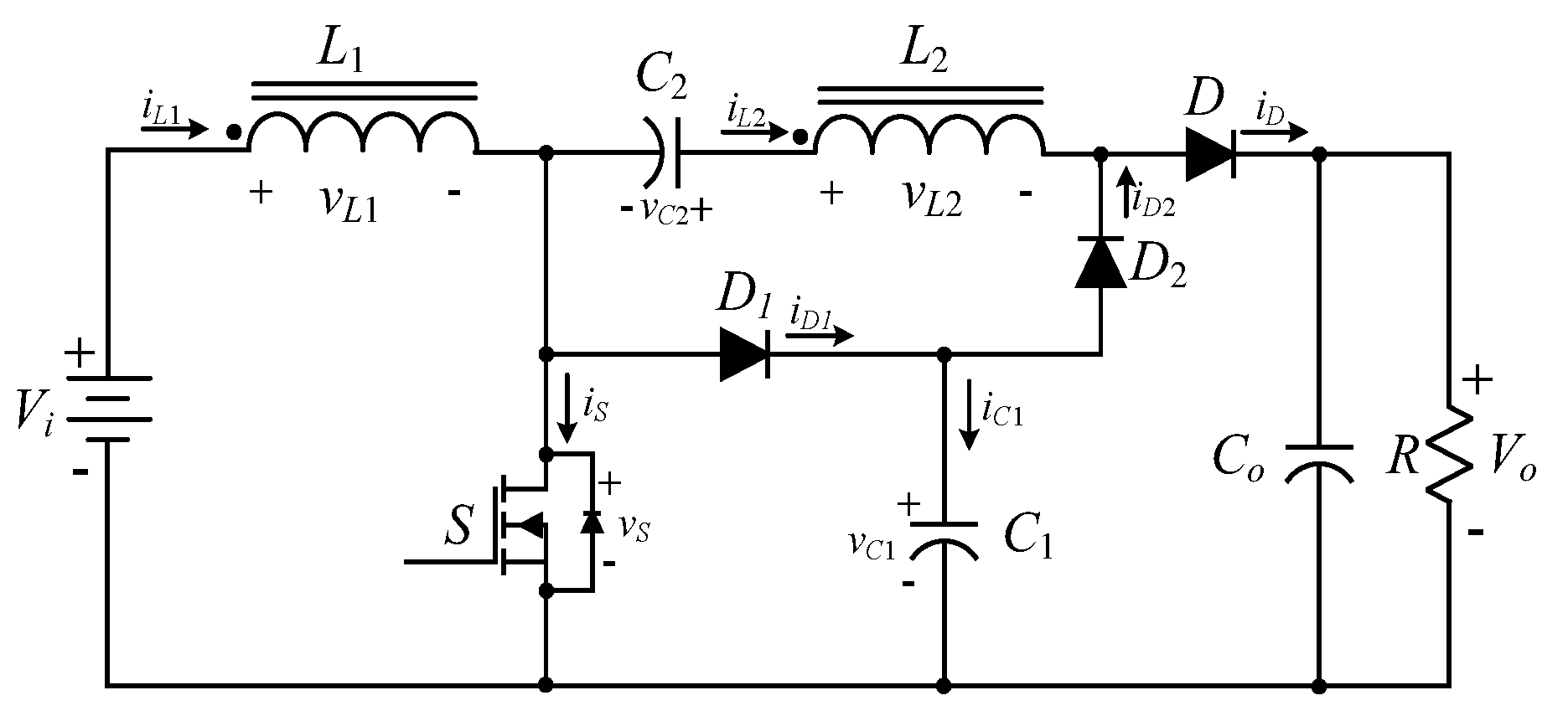
Figure 2.
Equivalent circuit when the main switch S is conducting in the high step-up hard switching converter.
Figure 2.
Equivalent circuit when the main switch S is conducting in the high step-up hard switching converter.
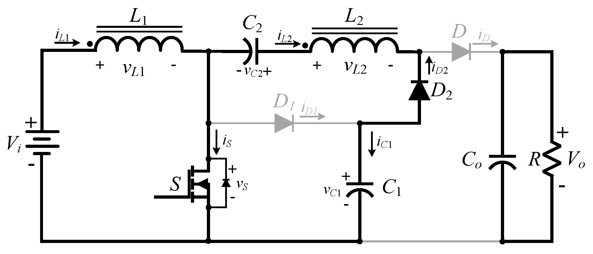
Figure 3.
Equivalent circuit of the high step-up hard switching converter when the main switch S is off.
Figure 3.
Equivalent circuit of the high step-up hard switching converter when the main switch S is off.
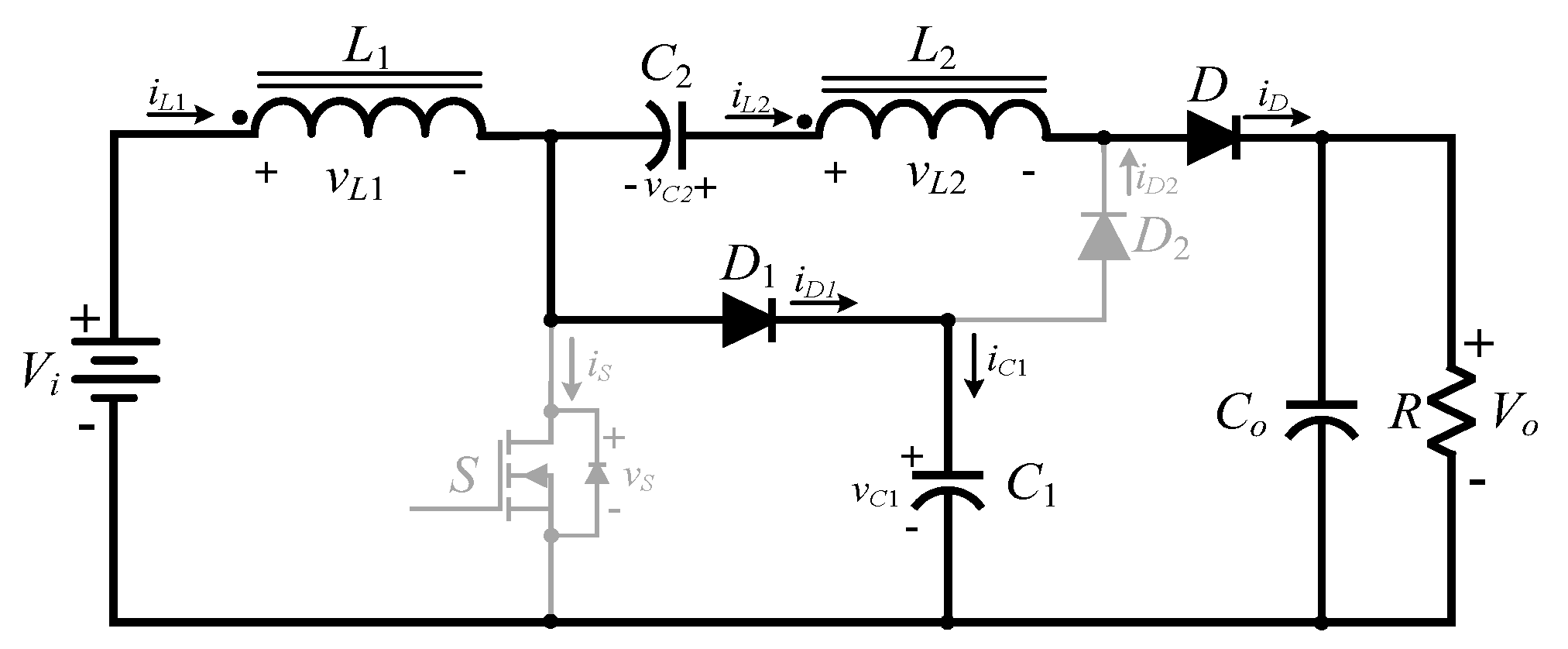
Figure 4.
Voltage gain vs. duty cycle curve for high step-up hard switching converter.
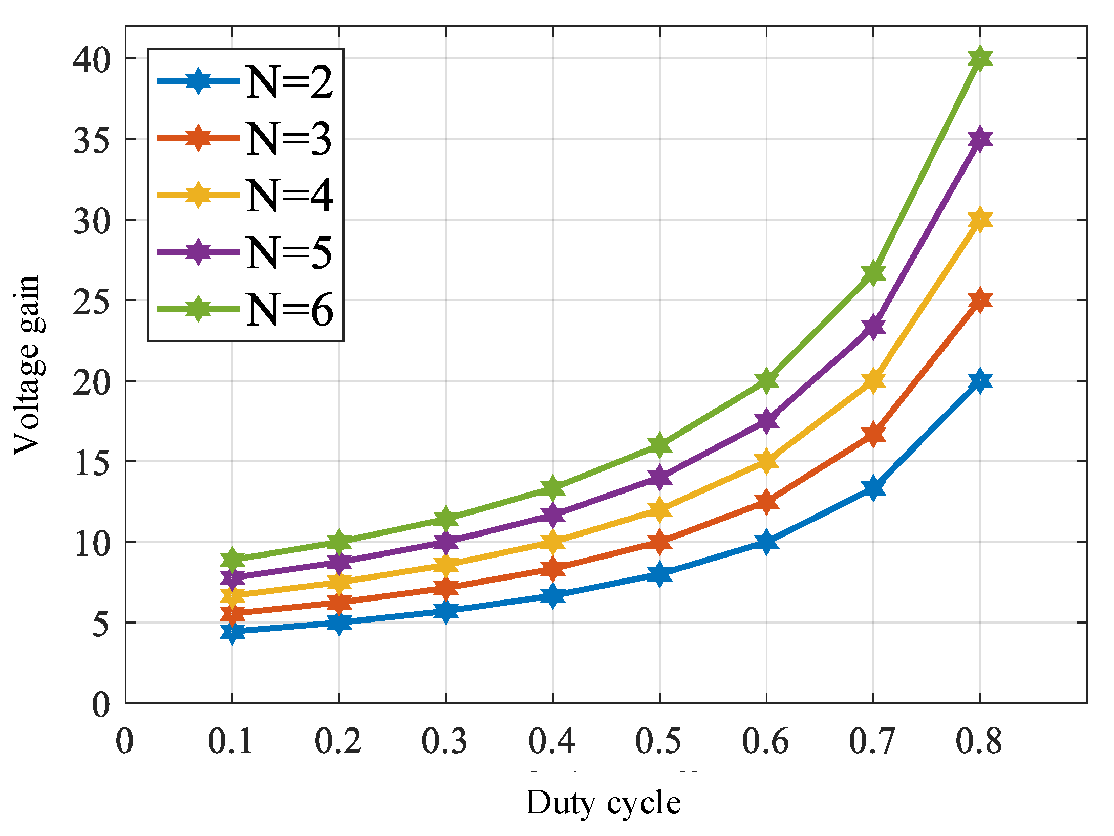
Figure 5.
Circuit architecture of the proposed high step-up soft switching converter.
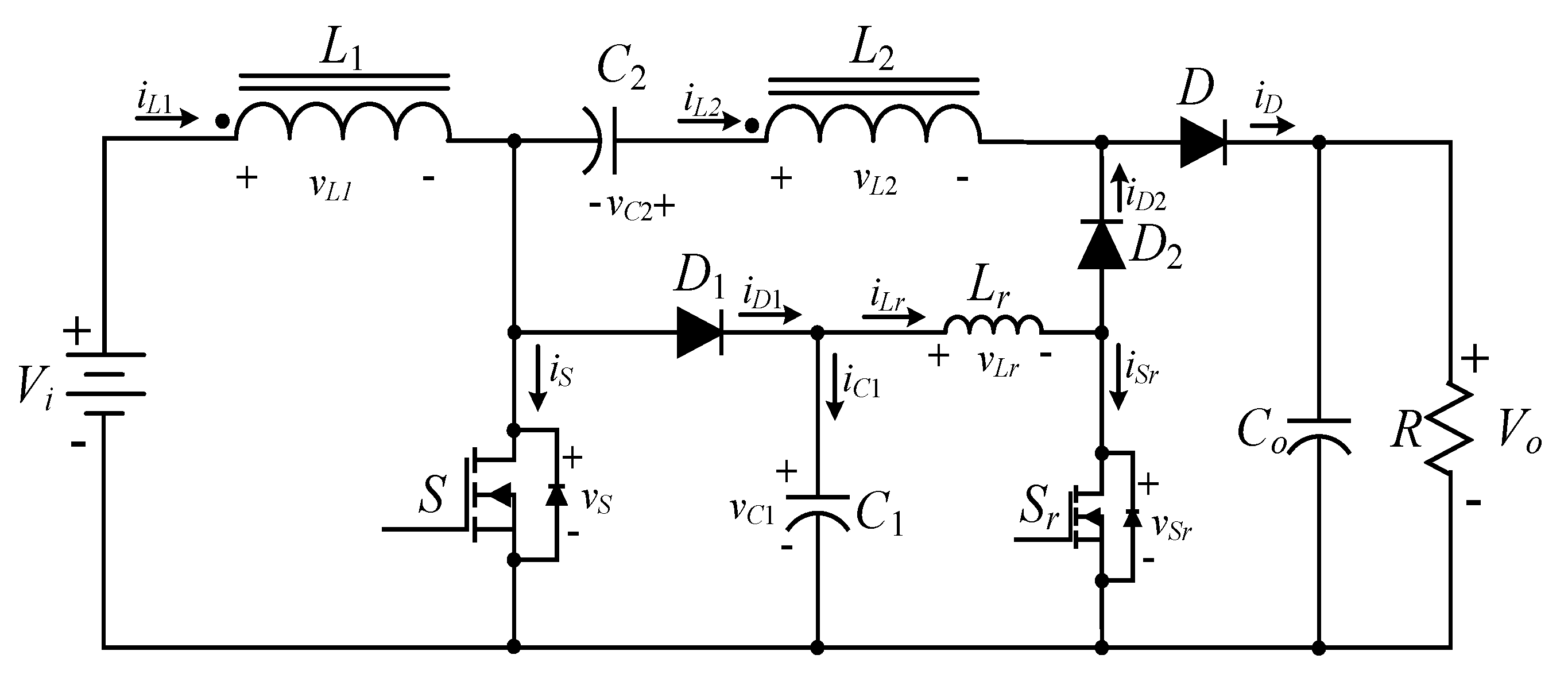
Figure 6.
Switching signal diagram of the high step-up soft switching converter [15].
Figure 6.
Switching signal diagram of the high step-up soft switching converter [15].
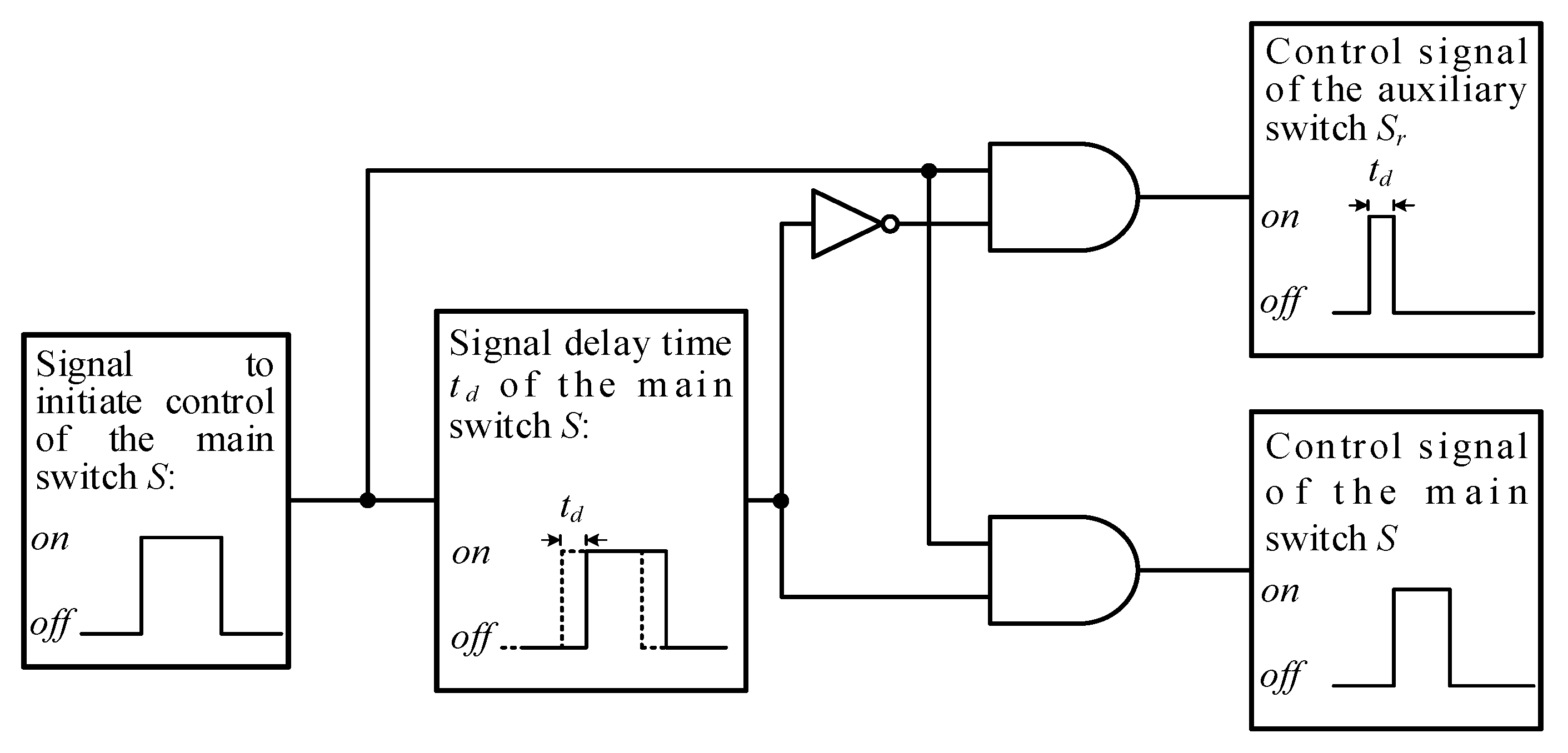
Figure 7.
Switching waveforms of each component in the proposed converter under different operating modes.
Figure 7.
Switching waveforms of each component in the proposed converter under different operating modes.
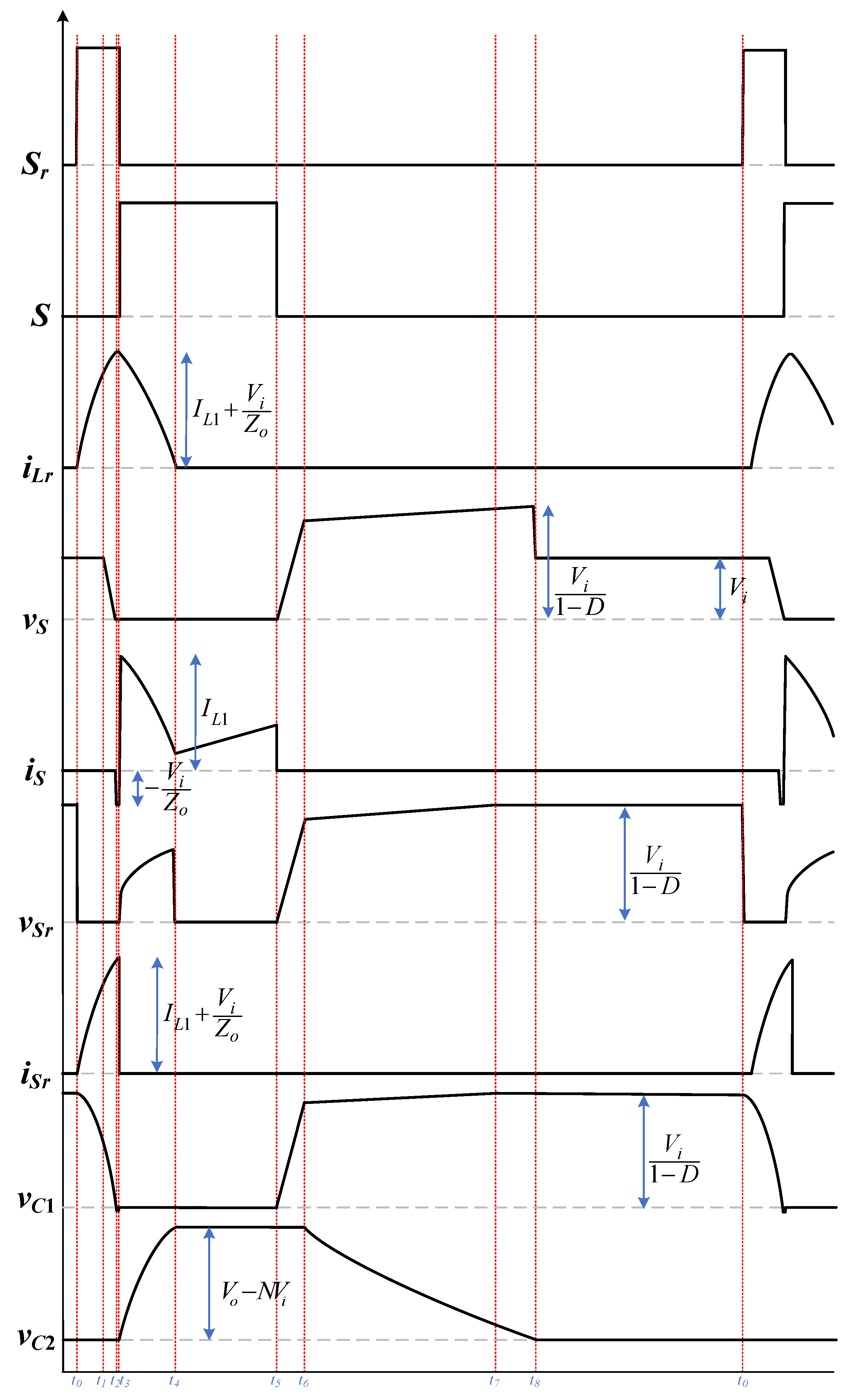
Figure 8.
Circuit conduction state in Mode 1.
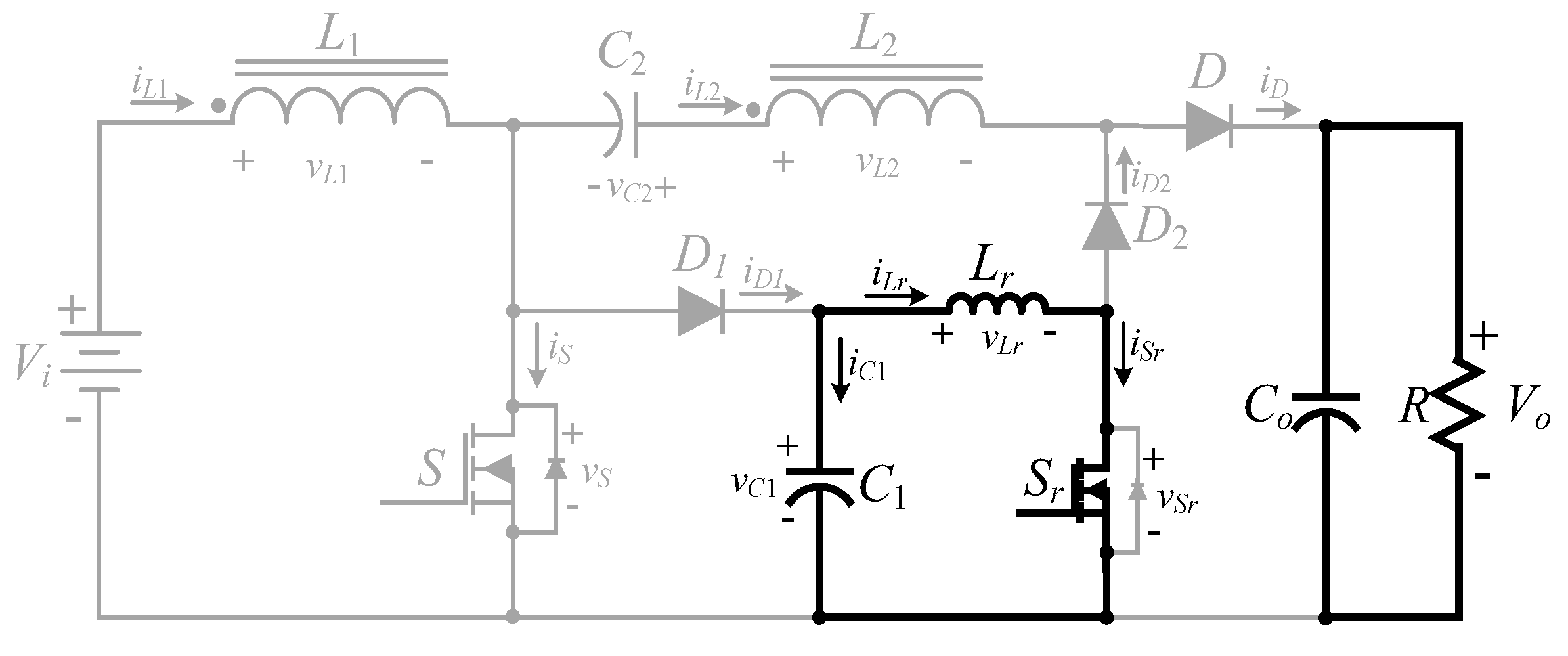
Figure 9.
Circuit conduction state in Mode 2.
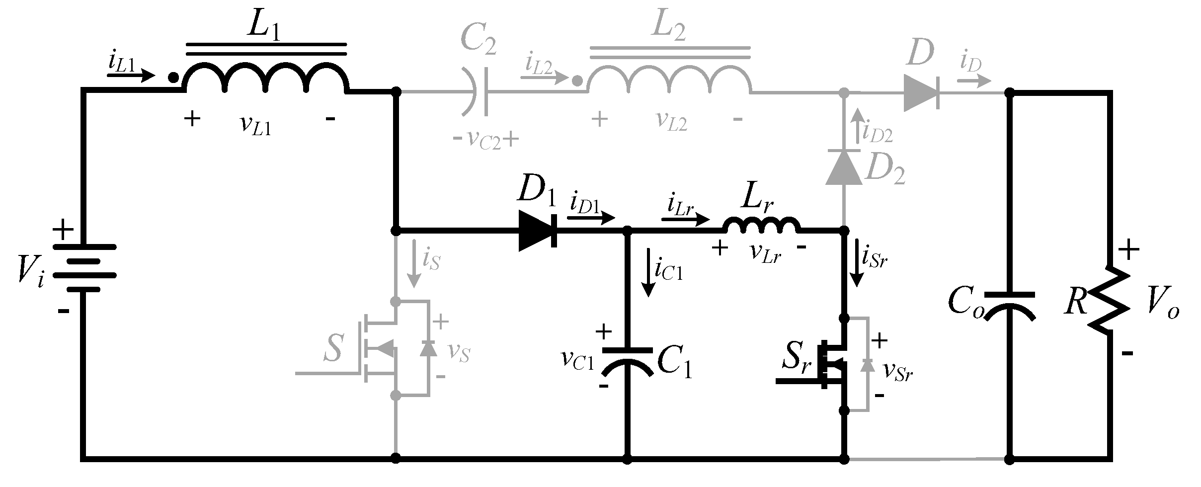
Figure 10.
Circuit conduction state in Mode 3.
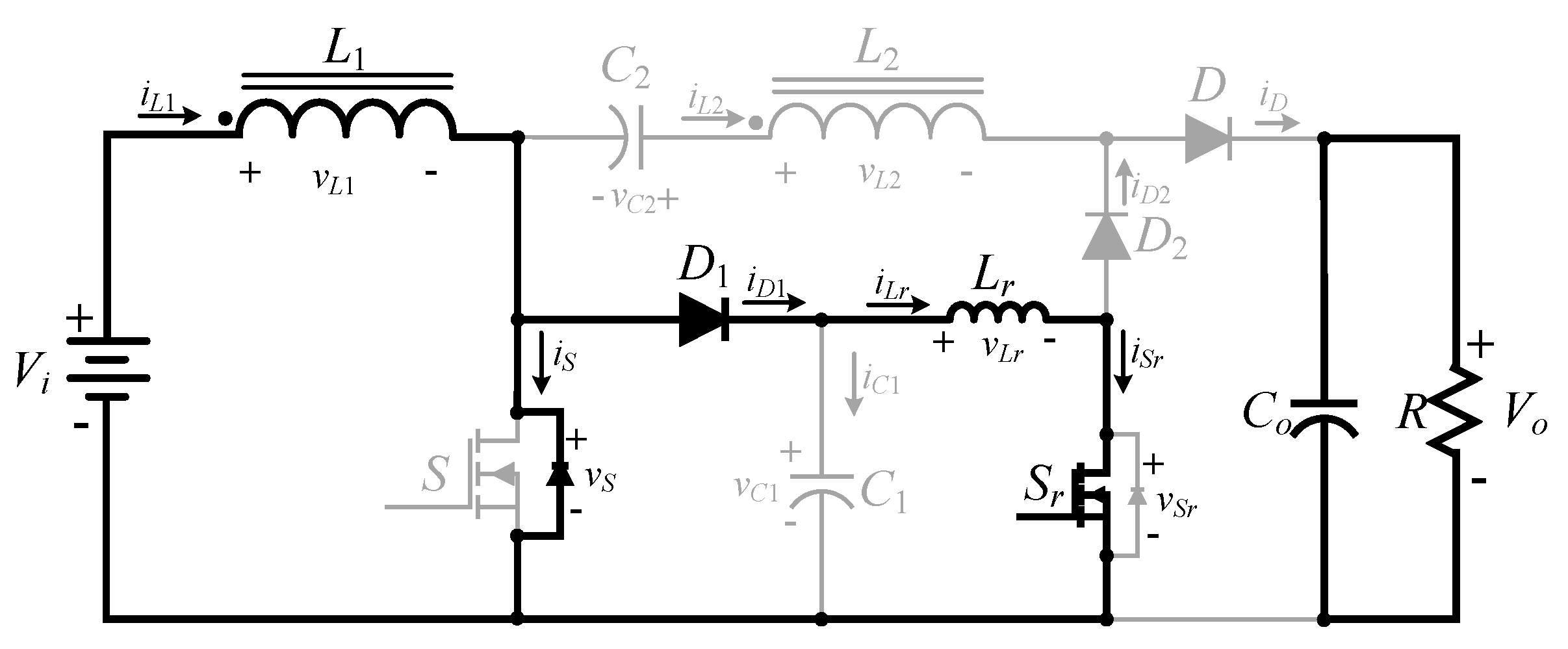
Figure 11.
Circuit conduction state in Mode 4.
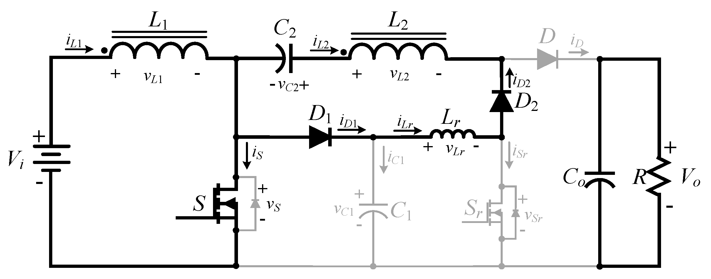
Figure 12.
Circuit conduction state in Mode 5.
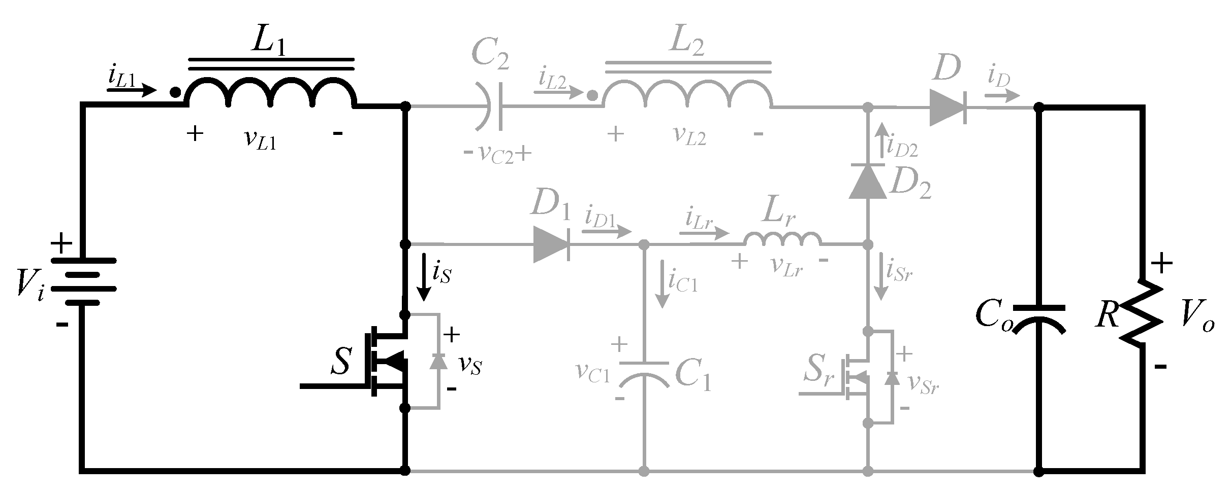
Figure 13.
Circuit conduction state in Mode 6.
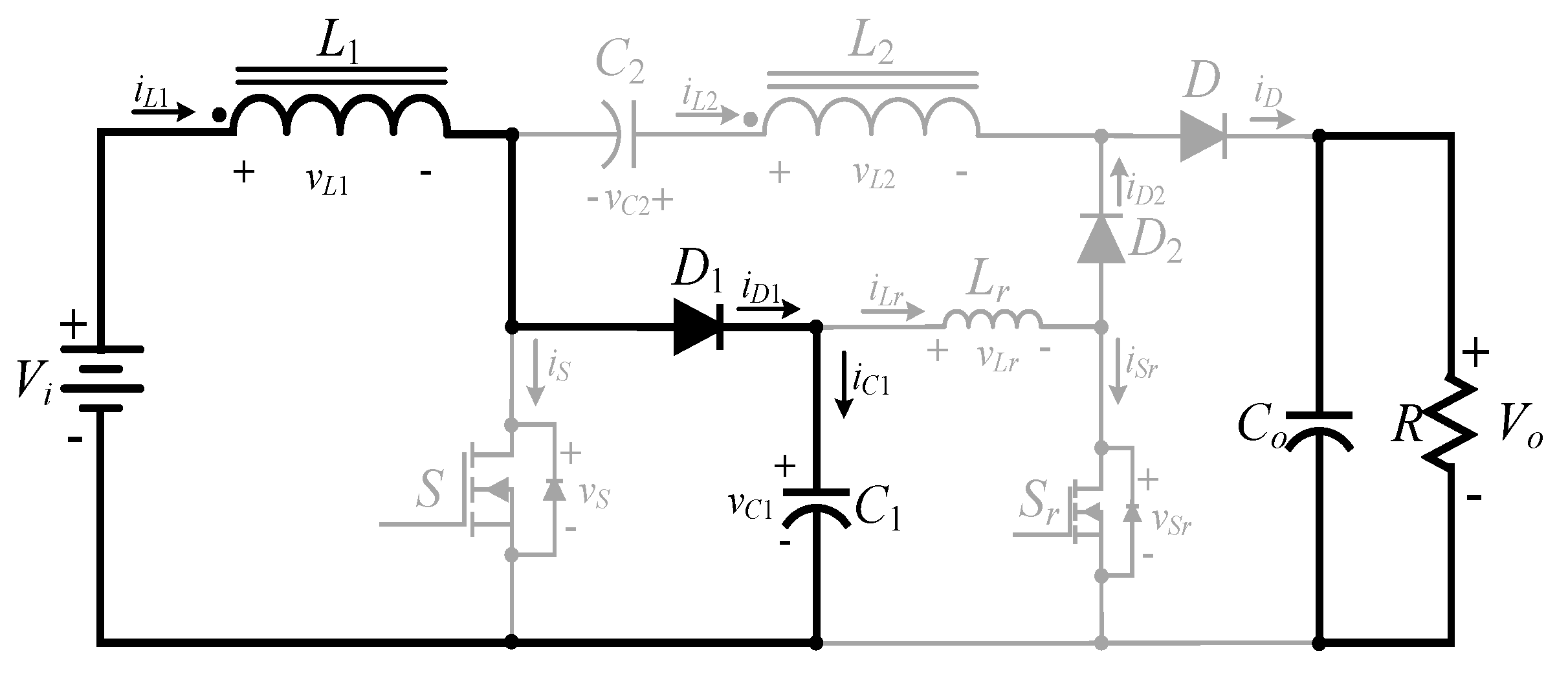
Figure 14.
Circuit conduction state in Mode 7.
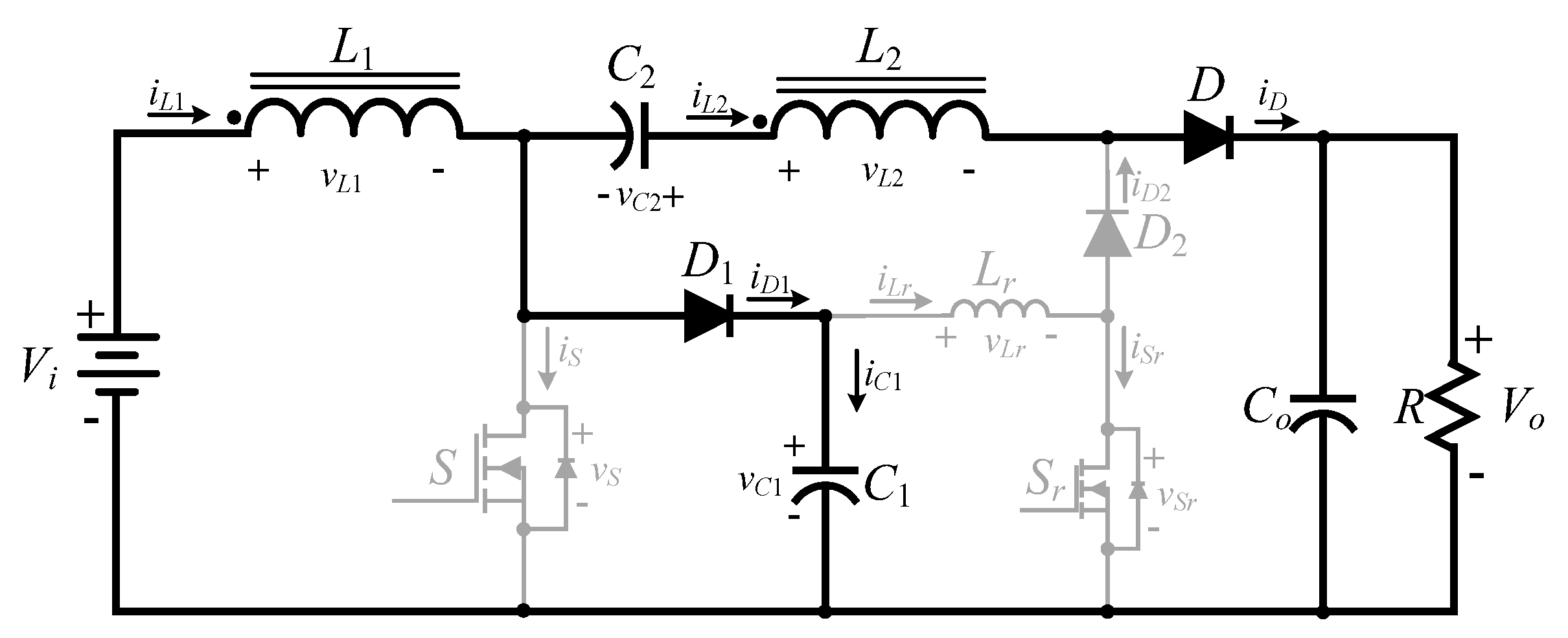
Figure 15.
Circuit conduction in Mode 8.
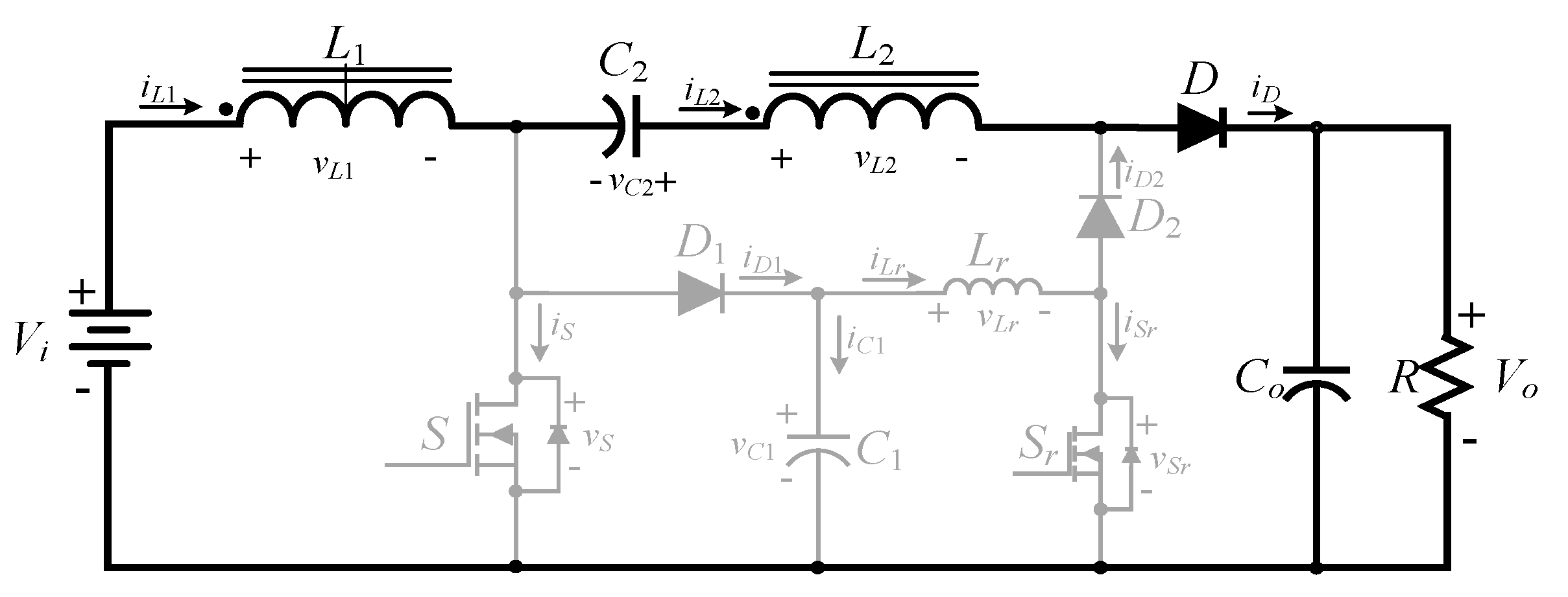
Figure 16.
Circuit conduction state in Mode 9.
Figure 17.
The relationship curve between the duty cycle D and the function.
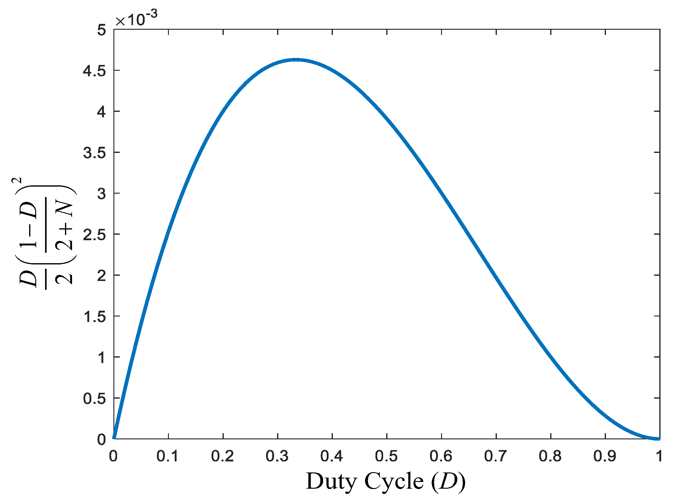
Figure 18.
Main switch control signal duty cycle, input voltage, and output voltage waveforms of the converter operating at full load (P=340W).
Figure 18.
Main switch control signal duty cycle, input voltage, and output voltage waveforms of the converter operating at full load (P=340W).
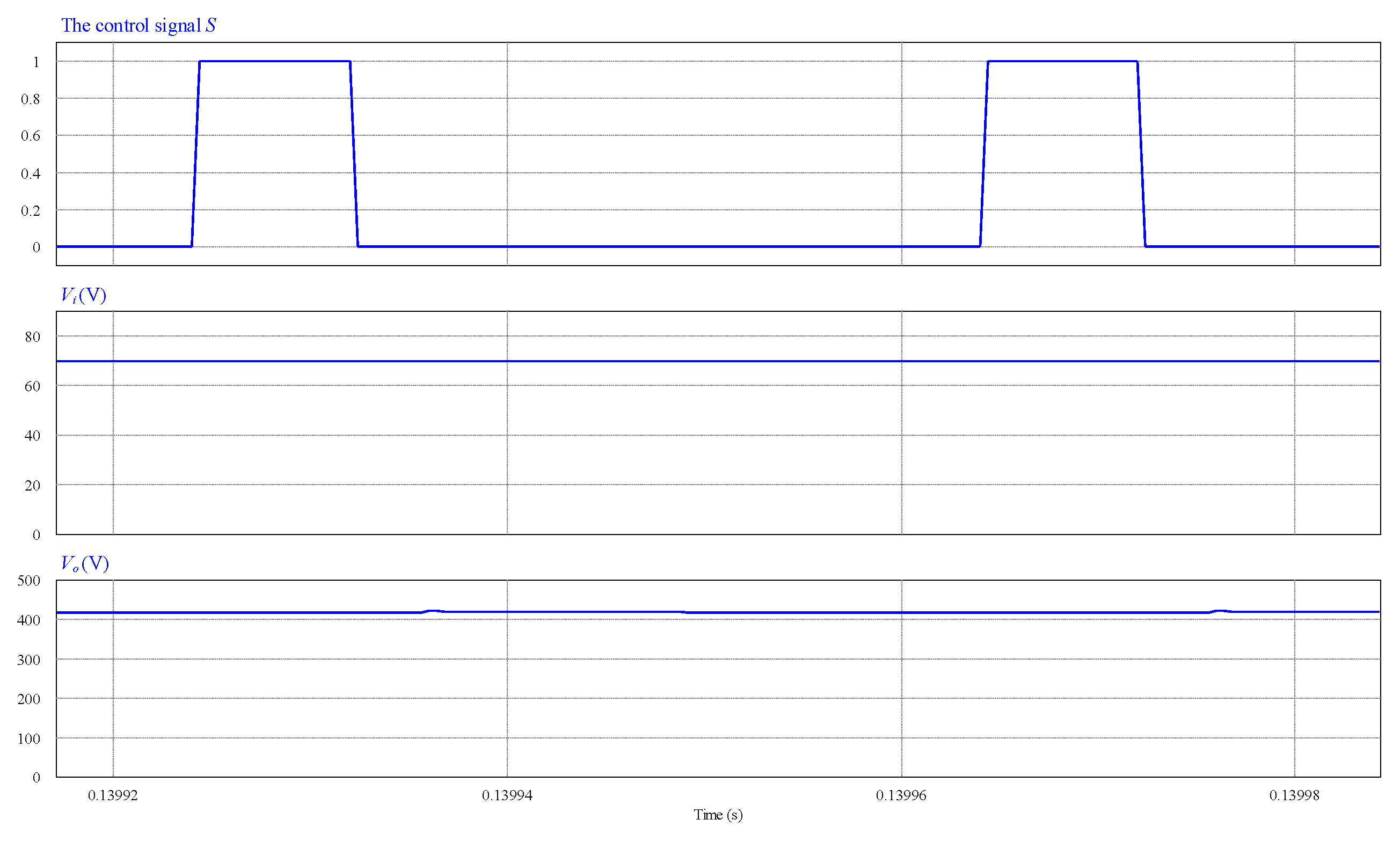
Figure 19.
Simulation waveforms of the electrical quantities for the main switch S at full load (P=340W).
Figure 19.
Simulation waveforms of the electrical quantities for the main switch S at full load (P=340W).
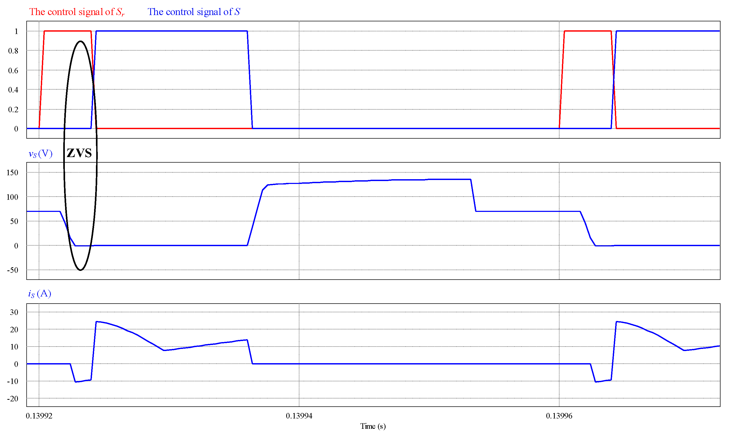
Figure 20.
Simulation waveforms of the electrical quantities for the auxiliary switch Sr of the converter when operating at full load (P=340W).
Figure 20.
Simulation waveforms of the electrical quantities for the auxiliary switch Sr of the converter when operating at full load (P=340W).
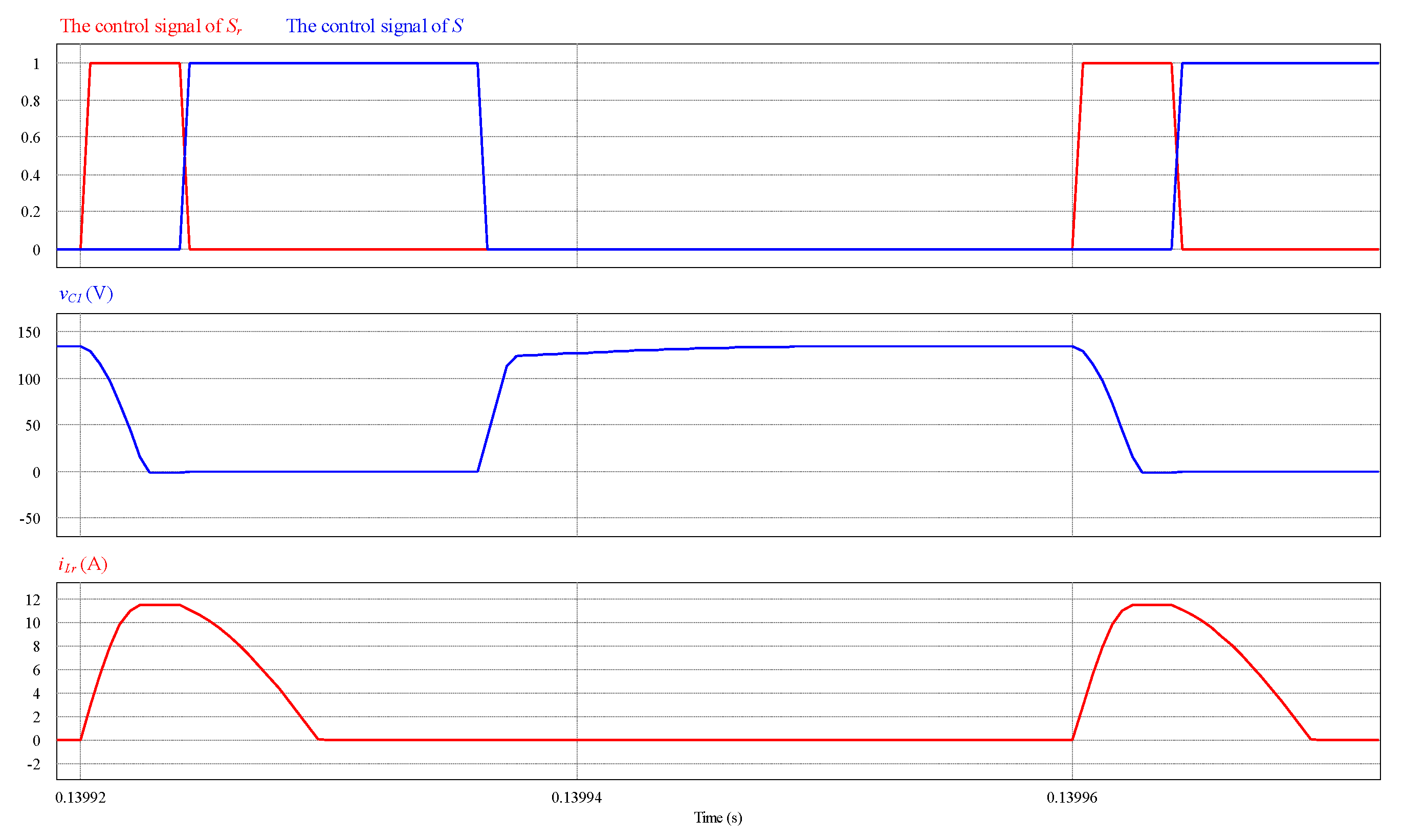
Figure 21.
Simulation waveforms of the electrical quantities for the main switch S at light load (P=100W).
Figure 21.
Simulation waveforms of the electrical quantities for the main switch S at light load (P=100W).
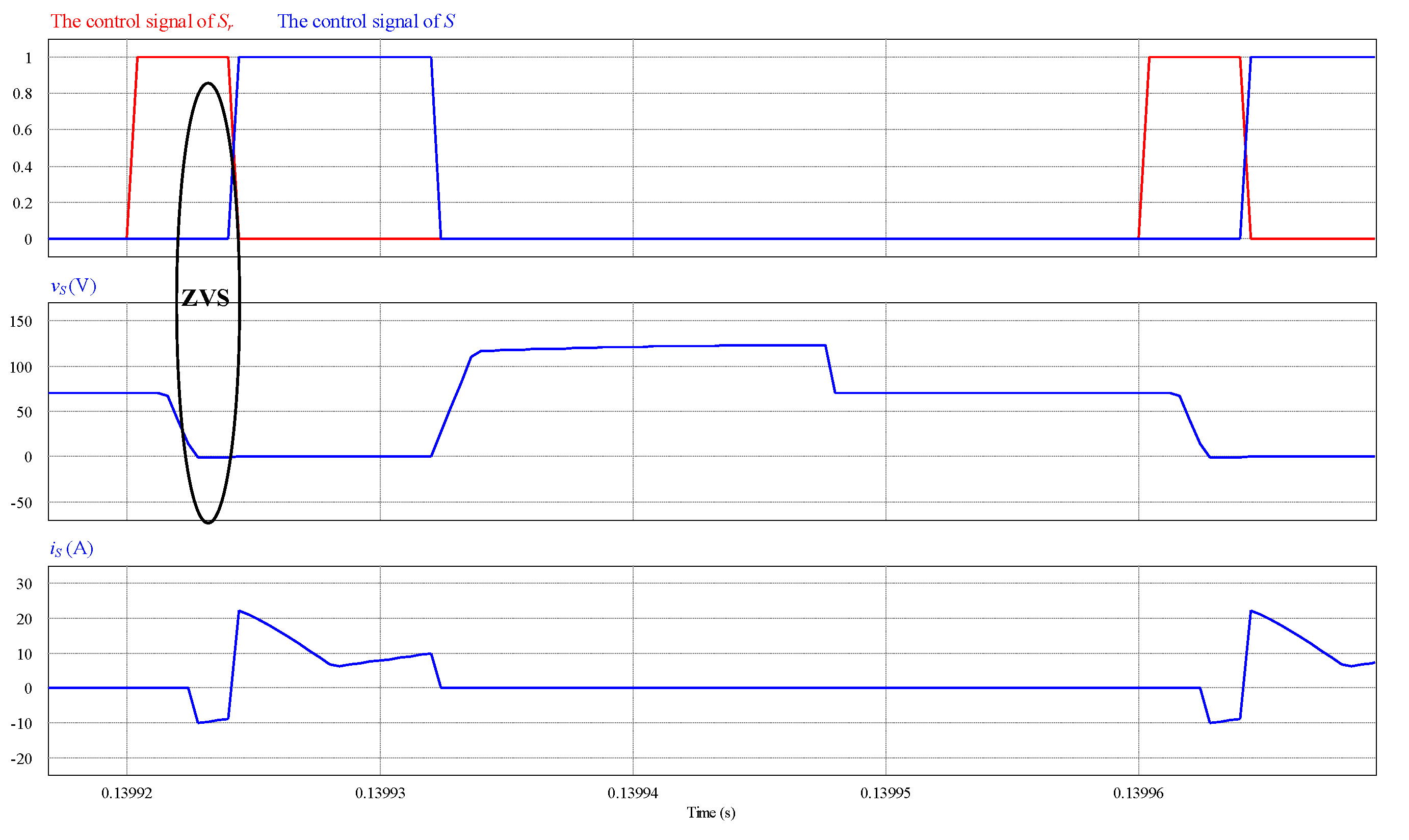
Figure 22.
Simulation waveforms of the electrical quantities for the auxiliary switch Sr of the converter at light load (P=100W).
Figure 22.
Simulation waveforms of the electrical quantities for the auxiliary switch Sr of the converter at light load (P=100W).
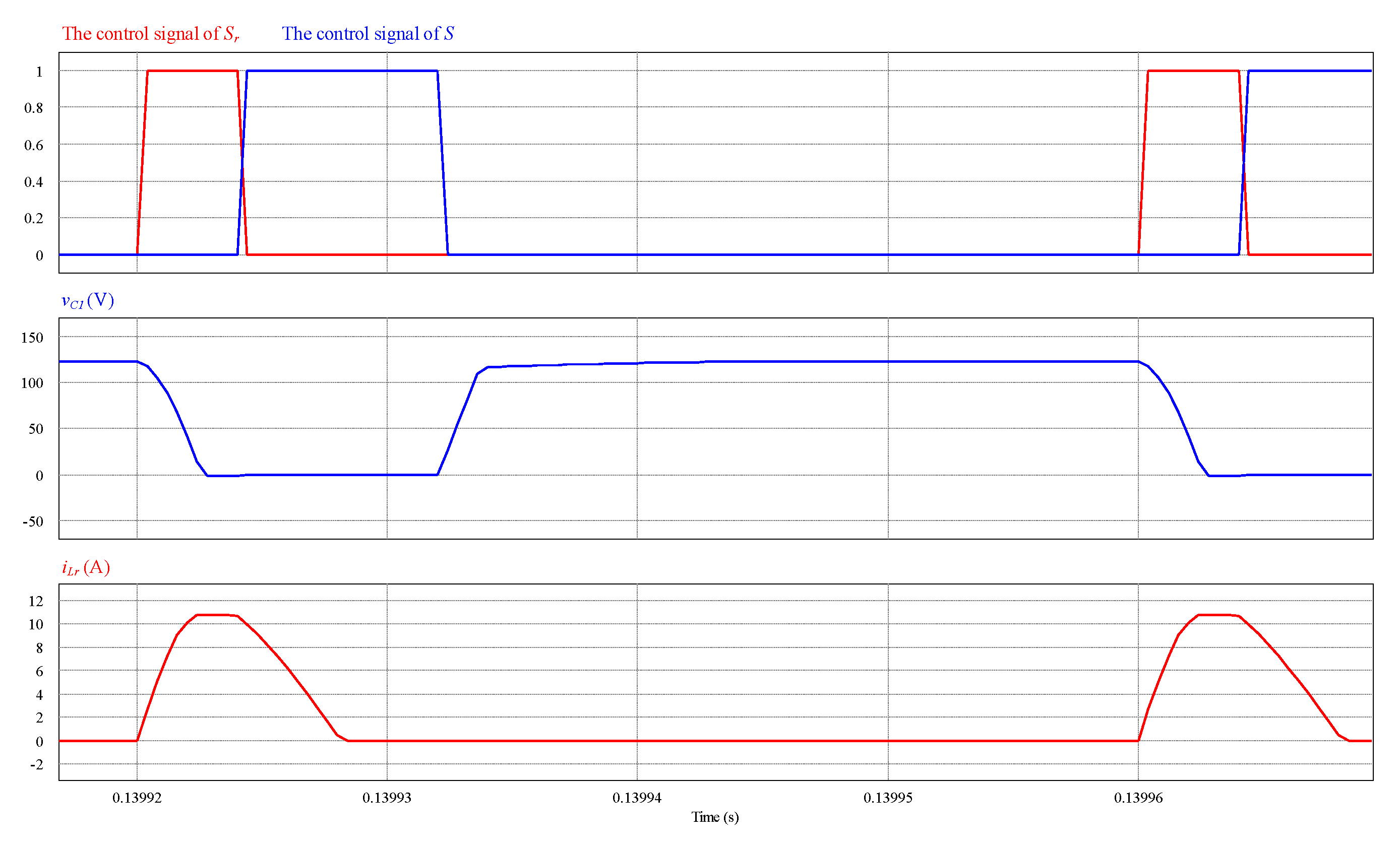
Figure 23.
Physical appearance of the high step-up soft switching converter circuit.
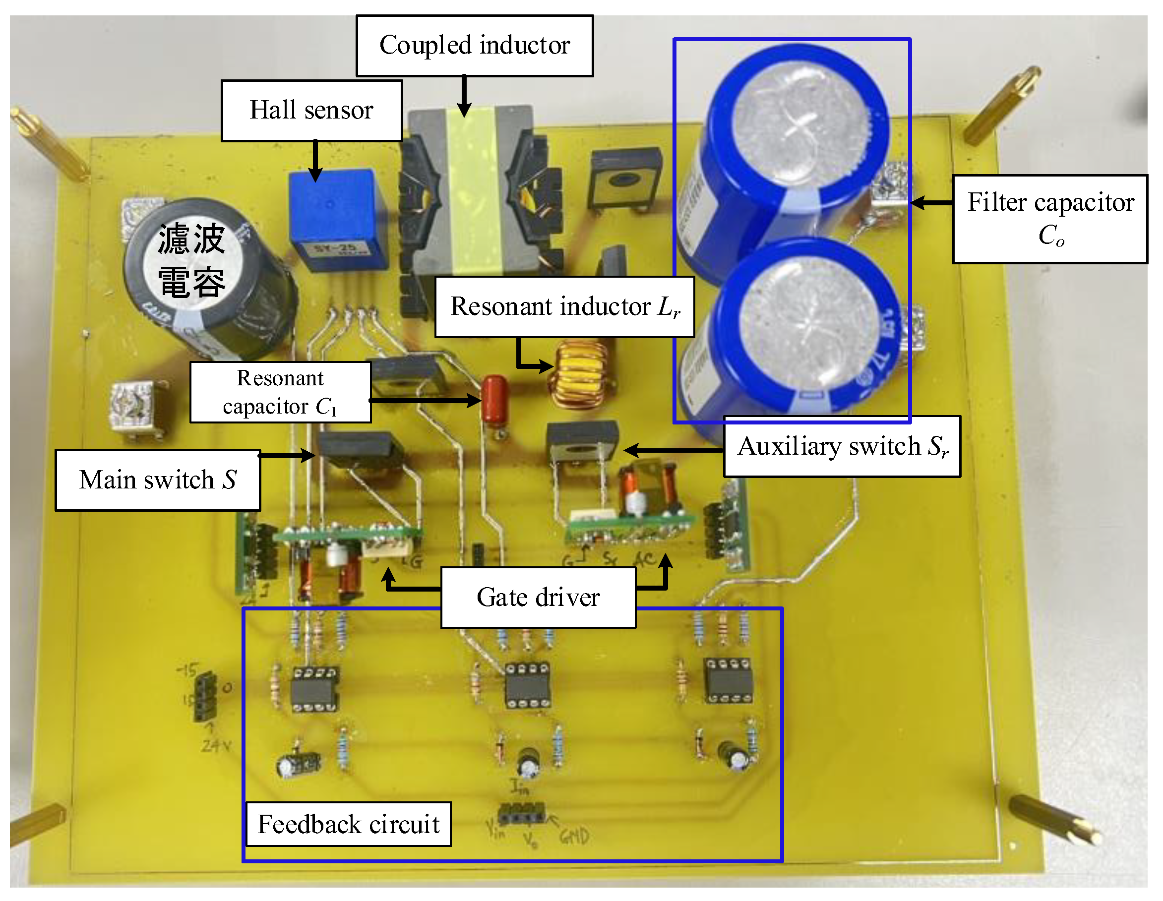
Figure 24.
Test platform for the high step-up soft switching converter.
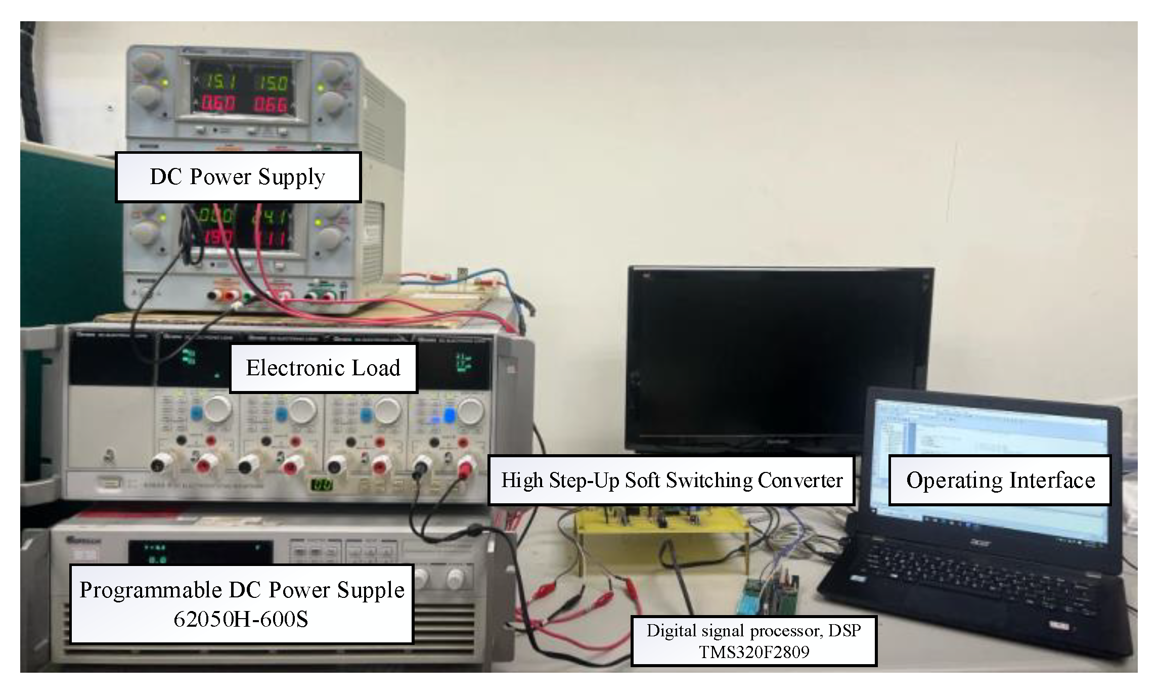
Figure 25.
Waveform of the trigger signal, input voltage, and output voltage of the main switch S when the converter operates under full load (P=340W).
Figure 25.
Waveform of the trigger signal, input voltage, and output voltage of the main switch S when the converter operates under full load (P=340W).
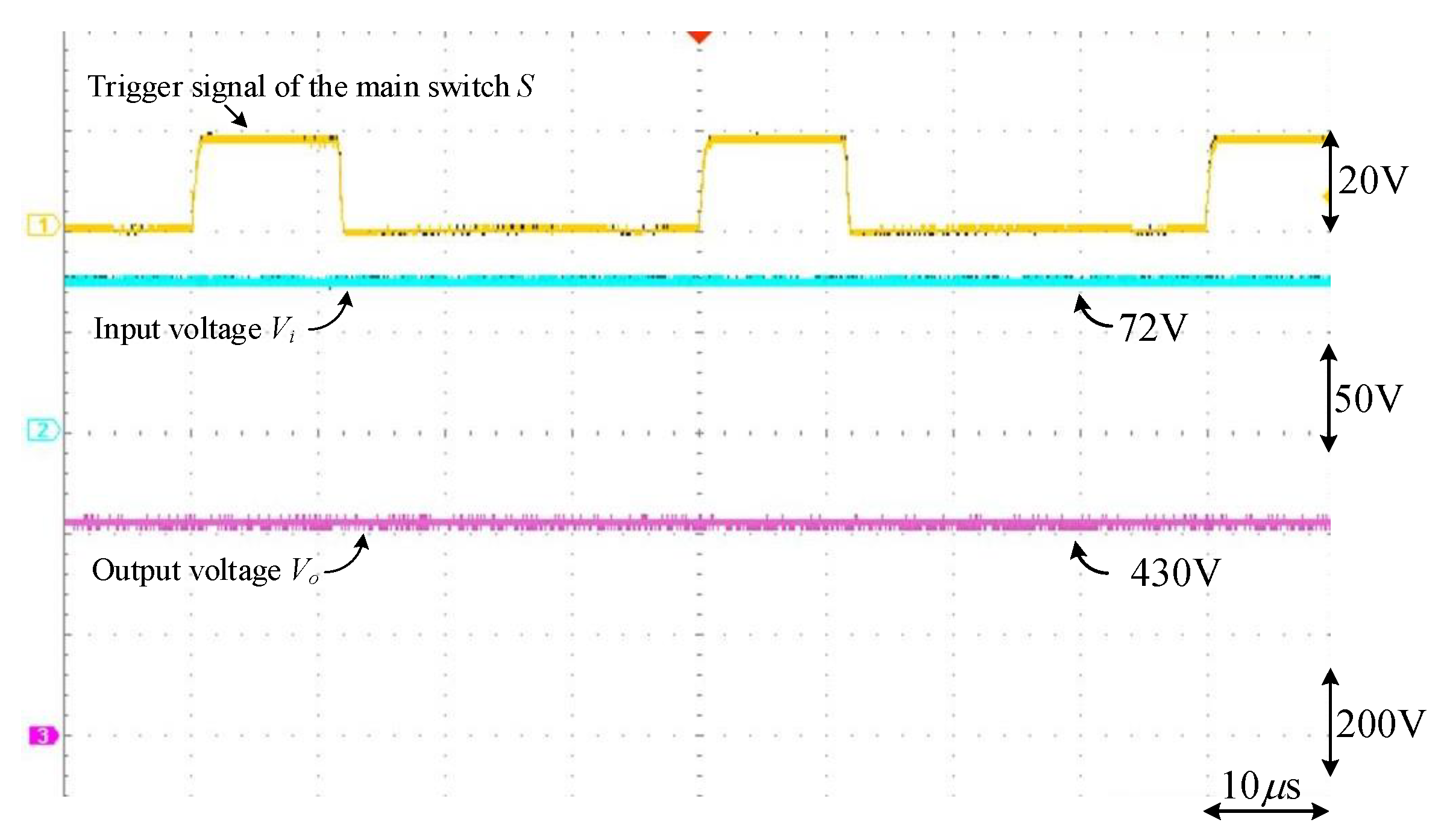
Figure 26.
Waveform of the trigger signal, voltage, and current of the main switch S under light load (P=100W).
Figure 26.
Waveform of the trigger signal, voltage, and current of the main switch S under light load (P=100W).
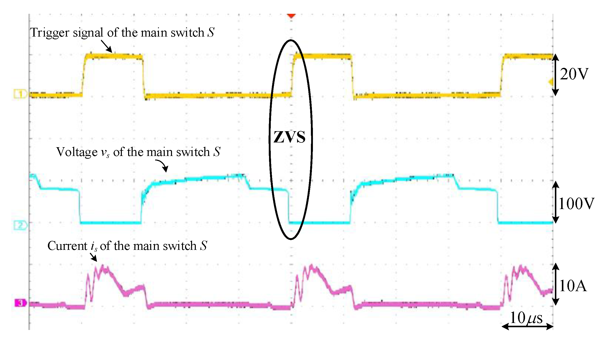
Figure 27.
Waveform of the trigger signal, voltage, and current of the auxiliary switch Sr under full load (P=100W).
Figure 27.
Waveform of the trigger signal, voltage, and current of the auxiliary switch Sr under full load (P=100W).
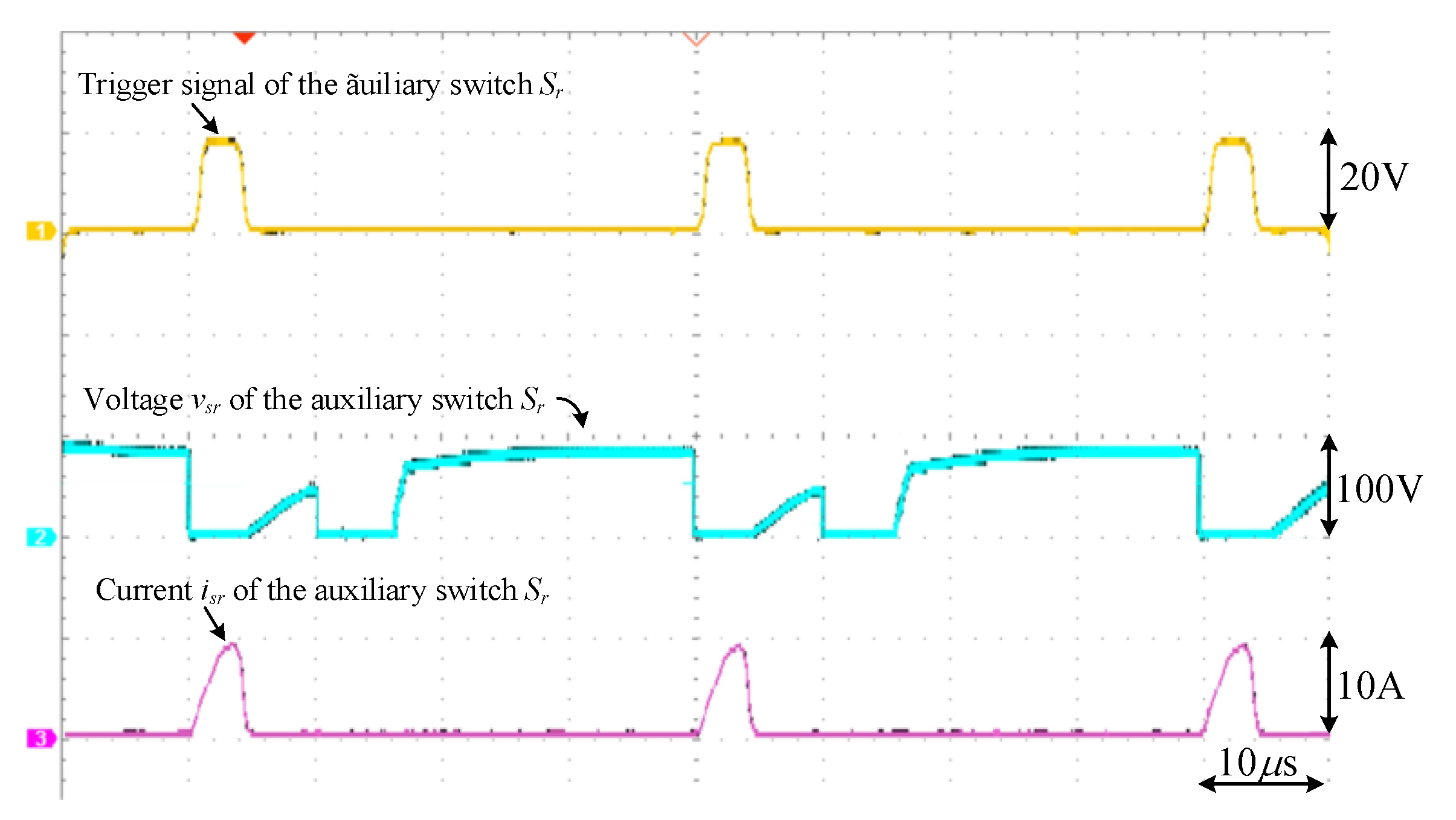
Figure 28.
Waveform of the trigger signal, voltage, and current of the main switch S under full load (P=340W).
Figure 28.
Waveform of the trigger signal, voltage, and current of the main switch S under full load (P=340W).
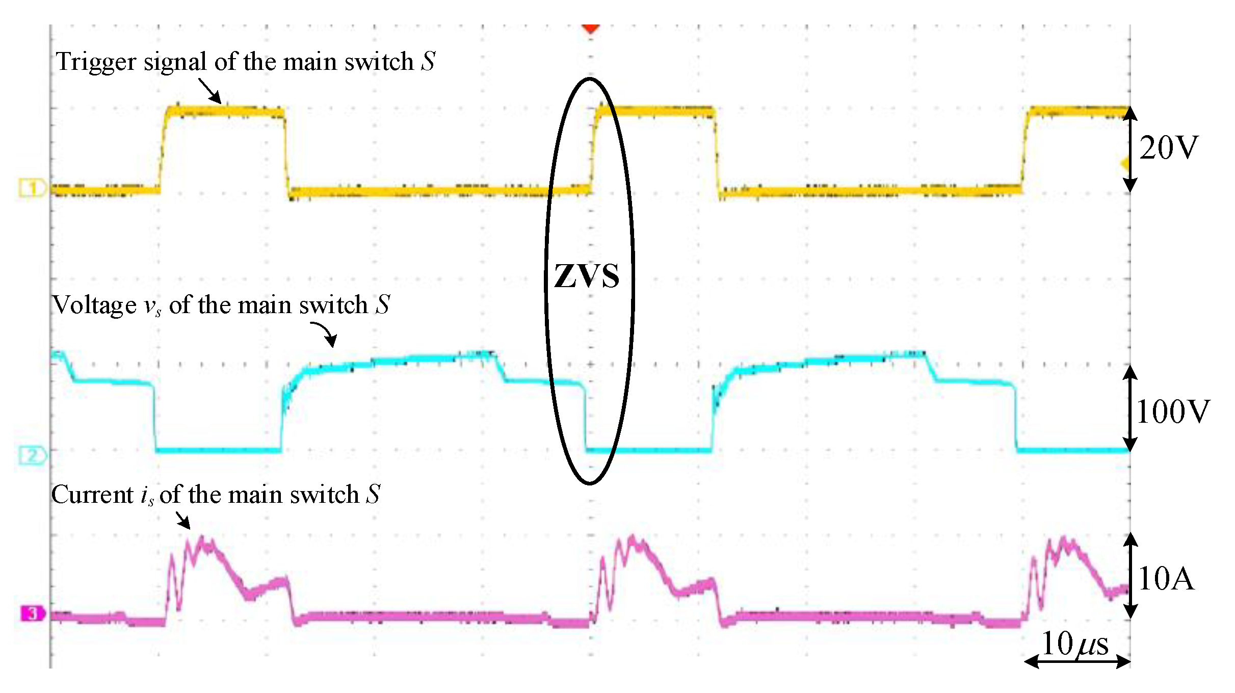
Figure 29.
Waveform of the trigger signal, voltage, and current of the auxiliary switch Sr under full load (P=340W).
Figure 29.
Waveform of the trigger signal, voltage, and current of the auxiliary switch Sr under full load (P=340W).
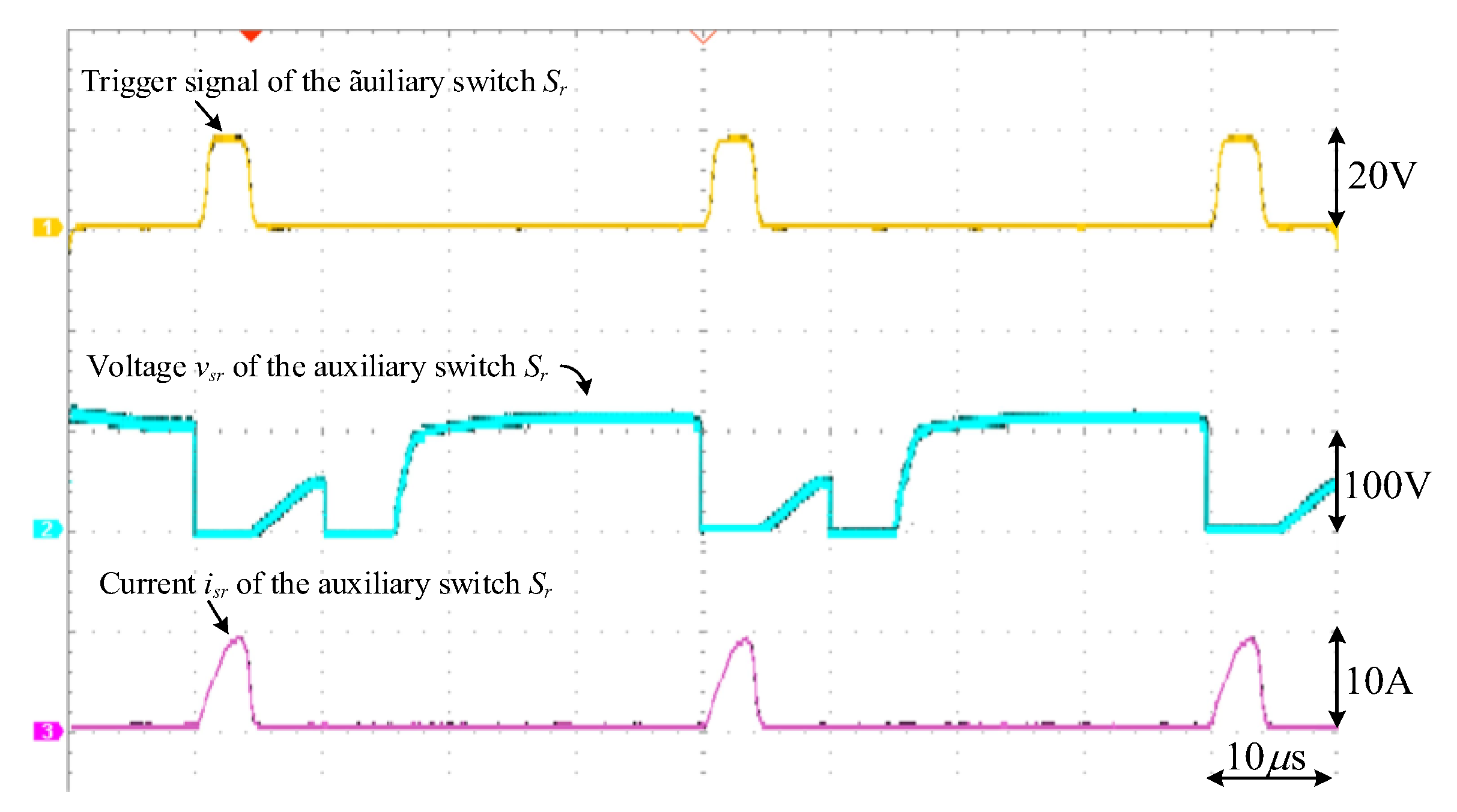
Figure 30.
Efficiency comparison between the high step-up soft-switching converter and the hard-switching converter.
Figure 30.
Efficiency comparison between the high step-up soft-switching converter and the hard-switching converter.
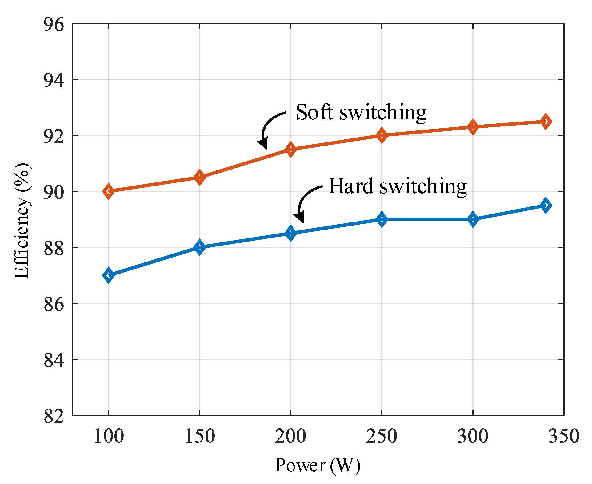

Table 1.
Relationship between voltage gain and duty cycle for the high step-up hard switching converter.
Table 1.
Relationship between voltage gain and duty cycle for the high step-up hard switching converter.
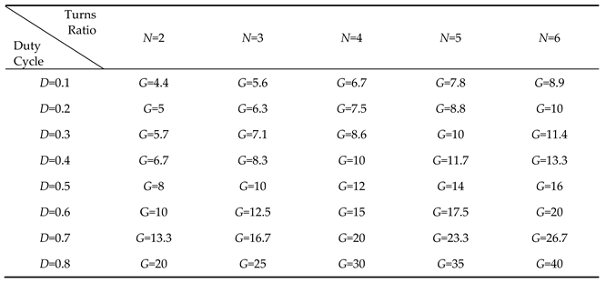 |
Table 2.
Component specifications of the high voltage ratio soft switching converter adopted.
| ConverterTopology | Converterin [4] | Converterin [5] | Converterin [6] | Converterin [12] | ProposedConverter |
|---|---|---|---|---|---|
| Voltage Gain | |||||
| Voltage Stress onMOSFETs | |||||
| MOSFETs | 2 | 4 | 2 | 2 | 2 |
| Diodes | 3 | 0 | 2 | 3 | 3 |
| Inductors | 1 | 1 | 2 | 2 | 2 |
| Capacitors | 4 | 4 | 4 | 3 | 3 |
Table 3.
Parameter specifications of the high step-up hard-switching converter.
| Input Voltage Vi | 72 V10% |
| Output Voltage Vo | 430 V |
| Output Power Po | 340 W |
| Switching Frequency f | 25 kHz |
| Turns Ratio of Coupling Inductor N | 2 |
Table 4.
Parameter specifications of the high step-up hard-switching converter.
| Component | Specifications |
| Coupled Inductor L1 | 127H |
| Resonant Inductor Lr | 18H |
| Main Switch S | MOSFET-TK49N65W(650V/49A) |
| Auxiliary Switch Sr | MOSFET-TK49N65W(650V/49A) |
| Fast Diodes(D, D1, D2) | IQBD30E60A1(600V/30A) |
| Filtering Capacitor Co | 340F/900V |
| Resonant Capacitor C1 | 0.33F/400V |
| Energy Storage Capacitor C2 | 0.33F/600V |
Disclaimer/Publisher’s Note: The statements, opinions and data contained in all publications are solely those of the individual author(s) and contributor(s) and not of MDPI and/or the editor(s). MDPI and/or the editor(s) disclaim responsibility for any injury to people or property resulting from any ideas, methods, instructions or products referred to in the content. |
© 2025 by the authors. Licensee MDPI, Basel, Switzerland. This article is an open access article distributed under the terms and conditions of the Creative Commons Attribution (CC BY) license (http://creativecommons.org/licenses/by/4.0/).
Copyright: This open access article is published under a Creative Commons CC BY 4.0 license, which permit the free download, distribution, and reuse, provided that the author and preprint are cited in any reuse.


