
Submitted:
26 May 2025
Posted:
28 May 2025
You are already at the latest version
Abstract
This paper introduces a non-isolated ultra-high voltage gain topology using the combination of the coupled-inductor-based inverting buck-boost converter (IBB) and voltage multiplier (VM) structure. In the proposed converter, an ultra-high step-up voltage gain can be achieved with a small duty cycle thanks to a coupled inductor and VMs. The voltage stress and the losses of the switches in the proposed converter are even less compared to other conventional topologies. Unlike other coupled-inductor topologies, a large voltage spike caused by the leakage inductance of the coupled inductor is smoothed by the capacitor in the voltage multiplier. In addition, ZVS turn-on for the switches and ZCS turn-off for the diodes can be achieved with the energy stored in the leakage inductance. A 360W (40V/380V) prototype converter is implemented to prove the advantages of the proposed converter, with a maximum efficiency of 98.4%.
Keywords:
coupled inductor
; inverting buck-boost
; non-isolated dc–dc converters
; ultra-high step-up
; ultrahigh voltage gain
; voltage multiplier
1. Introduction
Nowadays, renewable energy sources such as fuel cells (FCs) and photovoltaic (PV) modules have become important energy sources which can replace fossil fuels. However, due to their low output voltage characteristics, normally ranging from 24V to 48V, it is necessary to boost the voltage up to 380V, which is suitable for the DC link of a single-phase or 700V for a three-phase grid-tie inverter [1].
The simplest way to achieve high step-up voltage gain is by using an isolated converter by adjusting the turns ratio of the transformer. However, due to their disadvantages of high losses, large volume, and high cost, since a greater number of turns for the transformer is required, they are not a suitable choice for applications that do not require isolation between input and output [17].
Conventional non-isolated boost converters could be a candidate. However, in order to achieve high step-up voltage gain, they have to work with an extreme duty cycle, which leads to decreased efficiency and increased system cost since high voltage rating components have to be used due to high voltage stress [2].
Recently, many high step-up voltage gain topologies have been introduced [3,4,5,6,7,8,9,10,11,12,13,14,15,16,17,18,19,20,21,22,23,24,25,26,27,28,29,30,31,32,33,34,35,36,37,38]. They can be divided into two groups: single-inductor based converters [4,5,6,7,8,9,10,11,12,13,14] and coupled-inductor based converters [16,17,18,19,20,21,22,23,24,25,26,27,28,29,30,31,32,33,34,35,36,37,38]. Single-inductor based converters include interleaved boost or buck-boost converters [4,5,6], switched-inductor and voltage lift techniques [7,8,11,12], voltage multiplier (VM) and their combination topologies [13,14,15]. These types of converters can achieve higher step-up voltage gain than conventional ones with high efficiency. However, for an ultra-high step-up voltage ratio, more converter stages must be cascaded, resulting in the use of more components, which decreases efficiency and increases volume and cost.
Coupled-inductor based topologies can easily meet the high step-up voltage gain requirement by adjusting the turns ratio of the coupled inductor. However, there are still some issues that need to be solved to achieve high efficiency, high power density, and low cost, high turns ratio and leakage inductance of the coupled inductor, switching losses, and voltage stress on components.
The first issue is the high turns ratio of the coupled inductor, which leads to increased inductor volume and winding resistance, thereby reducing the power density and efficiency of the system. Moreover, the leakage inductance causes a very high voltage spike applied to the switches, resulting in high power losses and the need for high voltage rating components, thereby increasing the cost. The leakage inductance problem can be solved by using a passive snubber [16,17,18,19,20,21,22,23,24,25,26,27,28,33], or an active snubber [29,30,31,32], or passive clamping [36,37] so low voltage rating switches can be used with low internal resistance , hence increasing the overall efficiency. However, this requires more components, increases control complexity for the active snubber, and consequently increases the losses, volume, and cost of the converter.
Another issue that mainly affects the efficiency of the converter is switching losses. Even though the voltage spike applied to the switches caused by leakage inductance is eliminated, the efficiency of the converters in [16,18,31] is still low because of hard switching, resulting in high switching losses in the switches. Moreover, these losses are proportional to the increase in switching frequency. So, in order to maintain efficiency, the converter must work at a low switching frequency, which leads to larger required values for the capacitor and inductor, thus decreasing the power density. The topologies introduced in [21,23,24,26,27,29,30,32,33,35,36] can achieve soft switching to improve efficiency. In these converters, the snubbers or clamped circuits not only eliminate the voltage spike applied to semiconductor devices by absorbing the energy of the leakage inductance but also use this energy to provide Zero-Voltage Switching (ZVS) or Zero-Current Switching (ZCS) for the switches and diodes.
The third issue that increases the volume and cost of the converter is the voltage stress on components. Because of the asymmetrical configuration, the voltage stress on components in converters proposed in [16,17,18,19,20,21,22,23,24,25,26,27,28,29,30,31,32,33,34,35,37,38] are not evenly distributed. The components on the output side have higher voltage stress. So, all of them need to have higher voltage ratings, leading to increased volume and cost of the system. For example, the converter in [18] has voltage stress on output capacitor equal to output voltage and voltage stress on output diode is nearly equal to the output voltage. Similarly, the converter in [21] has the voltage stress on output diode nearly equal to output voltage.
In order to overcome all of these issues, the proposed converter has been introduced with the following features:
- Ultra-high step-up voltage gain with a low turns-ratio of the coupled inductor.
- ZVS turn-on for switches and ZCS turn-off for all diodes
- No voltage spike problem caused by leakage inductance without using an extra snubber circuit.
- Low voltage stress on all components due to the symmetrical configuration.
- Flexibly achieving higher step-up voltage gain with low duty cycle by either adjusting the turns ratio of coupled inductor or cascading a greater number of VM stages.
This paper is divided into six sections. The working principle of the proposed converter is presented in Section 2. The design procedure of the proposed converter is presented in Section 3. In Section 4, the experimental results demonstrating the superiority of the proposed converter are discussed. The comparison between the proposed converter and other topologies is shown in Section 5. Finally, the conclusion is in Section 6.
2. Proposed Converter Structure
2.1. Operating Principle
As shown in Figure 1, the proposed topology consists of two voltage multipliers (VM): positive VM (which includes diodes , and capacitors , ) and negative VM (which includes diodes , and capacitors , ) connected to the synchronous Inverting Buck-Boost (IBB) converter. Moreover, the main inductor of IBB is replaced by a coupled inductor, and the secondary side of the coupled inductor is placed at the common path between two blocking capacitors and of the positive VM and negative VM, respectively, not only for creating the ZVS turn-on for switches and ZCS turn-off for diodes but also to increase the overall voltage gain of the proposed converter. In the proposed topology, the leakage inductance referred to the secondary side is used for the ZVS condition, and its energy is absorbed by blocking capacitors and . Hence, no snubber is needed in the proposed topology. Furthermore, symmetrical configuration ensures that the voltage stress and current stress are evenly shared among all output components. Consequently, low-cost and small-volume components with low voltage ratings can be used.
In this section, the working principle of the proposed converter is described in Continuous Conduction Mode (CCM). From the key waveform shown in Figure 2, one switching cycle is divided into six modes based on the working status of the main switches. The equivalent circuit for each mode is shown in Figure 3. In the proposed two-stage converter, the main switches and the synchronous rectifier switches are synchronized in operation. To describe the operating principle of the proposed converter, the following assumptions are made:
- The circuit is operating in steady state mode, and the magnetizing inductor current is continuous.
- All the components are ideal, and the parasitic components are neglected.
- All the capacitors are large enough to maintain their voltages constant during a switch-off period.
- All the output capacitors have the same value (C1 = C2 = C3), and all the blocking capacitors have the same value (CS = CD).
- The switching period is Ts; the switch S1 is closed for time DTs and open for time (1-D) Ts and vice versa.
- The turns ratio of the coupled inductor and the relationship between the voltage of each winding are defined in (1)
Mode 1 (-)
Before , is off, and are reverse biased and , and were conducting. At = , turns off, the parasitic capacitor of is discharged. The coupled inductor starts to charge. Due to the charging of the parasitic capacitor of and the discharging of leakage inductor , the voltage across is raised up and the body diode of is forward biased to create the ZVS turn-on for .
Mode 2 (-)
At = , is off, the parasitic capacitor of is fully charged and that of is fully discharged. turns on with ZVS condition as created from Mode 1. Since the is fully on, its body diode is reverse biased, hence the current will flow through instead of its body diode. At the end of this mode, the is fully discharged, the current through the diodes and decrease to zero and ZCS turn-off for these diodes is achieved.
Mode 3 (-)
At = , is on, and is off, and the coupled inductor is being charged. Due to the secondary winding voltage of the coupled inductor, and are forward biased, and are reverse biased, causing capacitors and are discharged, is charged. During this mode, the leakage inductor stores the energy.
By using Kirchhoff’s Voltage Law (KVL), the equation expression in this mode can be expressed as follows.
By using Kirchhoff’s Current Law (KCL), the current of leakage inductor can be calculated as in (3).
Since the output current ripple is very small and can be neglected, the voltage of capacitor can be considered constant. Then the total ripple of the output voltage is only contributed by the voltage ripple of capacitors and . Moreover, from the earlier assumption, capacitors , , and have the same value. Then the leakage inductor current can be rewritten as follows.
And the voltage of the leakage inductor in this mode can be calculated as follows.
Mode 4 (-)
At = , turns off, turns on. The diodes and are reverse biased, and are forward biased. The body diode of is forward biased and conducted, the parasitic capacitor of is discharged and the parasitic capacitor of is charged. The coupled inductor and leakage inductor start to discharge. Due to the discharging of leakage inductor , the currents through diodes and are decreased and create ZCS turn off for these diodes. At the end of this mode, the leakage inductor is fully discharged.
Mode 5 (-)
In this mode, the energy stored in the core of coupled inductor is discharged to the output capacitor , and the blocking capacitor of negative VM is discharged to the output capacitor . The secondary side leakage inductor is charged after being fully discharged in Mode 3. The blocking capacitor of positive VM is charged for the next discharging cycle. The voltage applied to capacitor is not only the input voltage but also the voltage of primary and secondary winding of coupled inductor minus the voltage drop on leakage inductor while it is charging. Similarly, the voltage applied to the output capacitor is not only the voltage of blocking capacitor but also the voltage of secondary winding of coupled inductor resulting in the increasing of the overall voltage gain of proposed converter without increasing the voltage stress on components.
By using KVL, the equations of this mode can be expressed as in (6).
Mode 6 (-).
At = , the voltage of the capacitor is raised up higher to the primary winding voltage of the coupled inductor, the body diode of reverse biased. Hence the current flows through instead of its body diode. At the end of this mode = , one switching period is done, everything is ready for the next cycle.
The leakage inductor is charged in whole time of Mode 5 and Mode 6. Similar in Mode 3, the current flow through the leakage inductor can be calculated as in (7) by using KCL.
Hence, the voltage of the leakage inductor in this mode can be calculated as follows.
2.2. Steady State Analysis of the Proposed Converter
2.2.1. Voltage Gain and Voltage Stress on Components
Since Mode 1, Mode 2 and Mode 4 occur in a very short period of time, we can neglect these three modes in steady-state analysis. Hence, the period ( – ) will be and period ( – ) will be . Applying the voltage-second balance, the following equations can be obtained as in (9),
Hence, the voltage of capacitors can be calculated by using (10).
And the output voltage equation can be derived as in (11).
The voltage stress on semiconductors can be calculated as follows.
From (11) it is noted that the voltage gain is not only contributed by the VM stages but also by the turns-ratio of the coupled inductor. This means that we can flexibly achieve the ultra-high voltage gain by either cascading more VM stages, increasing the turn-ratio of the coupled inductor or both. Moreover, Equation (12) shows that the voltage stress is shared evenly among the components. Hence the output components will work with low voltage stress. This is an advantage of using the symmetrical configuration mentioned before.
2.2.2. ZVS Condition
In Mode 1, to achieve ZVS turn-on for , the voltage of leakage inductor , while it is discharging, must be larger than the sum of the voltage of blocking capacitor and secondary winding voltage as shown in (13)
The voltage of the leakage inductor can be found from the change of the current through it. As mentioned in Mode 1, the leakage inductor is fully discharged at the end of this mode. So, the change of the current in Mode 1 can be calculated as in (14).
The leakage inductance current at = actually is the leakage inductance current at = of the previous switching period and can be derived as in (15).
Then the ZVS condition equation can be expressed as in (16).
From (8) and (13), the value of secondary side leakage inductor can be calculated as follows.
As mentioned at the beginning of part B, the period ( – ) is denoted by , then (17) becomes (18).
where: is the discharging time of secondary side leakage inductor.
3. Design of the Proposed Converter
3.1. Design of the Output Capacitors
The output capacitors can be calculated from the maximum allowable output ripple voltage as in (19).
where: is switching frequency, is the output current, and is the equivalent output capacitor, that can be calculated as in (20).
To keep the symmetrical configuration, all the output capacitors must have the same value and can be calculated as in (21).
The leakage inductors , duty cycle D, and the dead time .
Firstly, the minimum duty cycle can be calculated from the required voltage gain in the case when the leakage inductor equals to zero.
The voltage of blocking capacitor in the case of minimum duty cycle can be calculated as follows.
By using (18) and (23), the minimum required value of leakage inductor can be calculated with an assumption that the discharging time is equal to the deadtime of switches.
After choosing the value for leakage inductor , the right value for duty cycle can be found from the output voltage equation shown in (11).
It should be noted that, if the value of the leakage inductor is too large, the voltage gain will be reduced much. Moreover, the has to be turned on before the leakage inductor gets fully discharged, then the dead time of switches must be smaller than the discharging time of the leakage inductor to maintain ZVS condition.
In mode 1, since the body diode of and are forward biased, the leakage inductor will resonate with capacitor . To maintain ZVS condition, the resonant frequency must be much smaller than switching frequency. Moreover, as an assumption before, the capacitors and have the same value to keep the symmetrical configuration, those values can be calculated by using (24).
3.2. Design of the Main Inductor
The magnetizing inductance of coupled inductors is designed to operate the proposed converter in CCM mode. Then its value can be calculated as in (25).
where: is the current ripple of the magnetizing inductor .
Then, the primary winding inductance and secondary inductance can be expressed by using (26).
4. Experiment Results
In order to verify the validity of the proposed converter, a 380V, 360W prototype converter is built for a photovoltaic module (Hyundai RI Series 360W, 72 Cell Solar Module). The specifications of the proposed converter are shown on Table 1, and the information about the switches and passive components are shown in Table 2.
In the experiments, the gate signals (, ) are generated by a DSP TMS320F28335. The prototype converter is shown in Figure 4. All the through-hole components are placed on the top side, the gate drivers are placed on the bottom side. All the capacitors are film capacitors.
The duty cycle of the main MOSFET () is 0.52 to boost the input voltage 40V to the output voltage of 380V. The deadtime between the two switches is 100ns.
The experimental results in full load condition are shown in Figure 5. In Figure 5(a), it is clear to see that is turned on with ZVS condition. The waveform in Figure 5(b) shows the body diode of is forward biased at the first part of on-time of (as in Mode 4 of working principal part) and it is reverse biased then the current is changed the direction at the last part of on-time of (as in Mode 5 of working principal part). Figure 5(c) and (d) show the voltage and current waveforms of the diodes. It is obvious that all the diodes are turned off with ZCS. Figure 6 shows the voltage and current waveforms of switches and diodes in light load (20%) condition. The switch still achieves ZVS turn-on, and the diodes still achieve ZCS turn-off as in full load condition. It is strong evidence to show the proposed converter can achieve ZVS turn on for switches and ZCS turn-off for diodes in the whole range of load. It should be noted that the oscillation of current when switches are off is observed because of a small snubber capacitor used to eliminate the hot-loop issue in half-bridge configuration.
Figure 7 shows the waveforms of output capacitors. Due to the symmetrical configuration, the voltage of output capacitors and of two voltage multiplier stages are the same. And the voltage of the IBB output capacitor is lower as compared to those of voltage multipliers as a result of the small duty cycle. Moreover, from Figure 7(b), it shows that the capacitors and are interleaved with each other, then their voltage ripples will be canceled out each other and then contribute to the low voltage ripple for output voltage. Hence the smaller value output capacitor can be used to achieve the required output voltage ripple.
Figure 8(a) shows the voltage waveforms of the diodes and MOSFET . These waveforms are exactly matched with the simulation. In Figure 8(b) zoomed in voltage waveforms of diodes and MOSFET , it is observed that the MOSFET is turned on before the diodes and turn on, and and turn off, at the period of 160ns, which is 60ns longer than the dead time of switches. This is the required time to achieve ZVS turn-on for and ZCS turn-off for diodes as explained before in Part II.
Figure 9 shows the waveforms of coupled inductors at full load. It can be noted that the leakage inductor is discharging causing high voltage spikes in secondary winding of the coupled inductor in a small period of time before the voltage of the coupled inductor changes its polarity. It is another requirement for ZVS turn-on for and ZCS turn-off for the diodes.
A Power analyzer (Xitron 2802) is used for measuring the converter efficiency. Figure 10 shows the measured efficiency plot of the proposed converter when VS = 40 V, VO = 380V and =100 kHz. As shown in Figure 10, efficiency achieves 97% at light load (20% load) and 96% at heavy load (100% load). The maximum efficiency of 98.4% is obtained at 150W.
5. Comparison Study
The comparison between the proposed converter and other converters is shown in Table 3. From Table 3, it is clear that the proposed converter has the highest efficiency with a low voltage stress on components and a low number of components. The voltage gain comparison is shown in Figure 11 for the turns-ratio of 1.05. The converters in [16,21,31,34,36,37,38] have higher voltage gain than the proposed topology. However, the voltage stress on output diodes and capacitors is much higher, and the efficiency is much lower than that of the proposed converter. Therefore, it can be concluded that the proposed converter has superior advantages compared to other new topologies. Moreover, the converters in [21,31,34] have a small range of duty cycle, from 0.1 to 0.5. Thus, with applications requiring several hundred watts and very high step-up voltage conversion, the current stress on components will increase significantly, leading to a reduction in the efficiency of the converter. From Figure 12, the comparison of the graphs of stress on diodes with different converters is shown with the proposed converter.
6. Conclusions
In this paper an ultra-high step-up converter using coupled inductor with low voltage stress on components and high efficiency while achieving a high step-up voltage gain characteristic is proposed. The proposed topology is advantageous in terms of the following features:
- No spike voltage applied to semiconductor devices and hence no need for extra snubber.
- Very high efficiency with ZVS turn-on for MOSFET and ZVZCS for diodes.
- Reduced voltage stress on the components due to the symmetric configuration.
- Easy to get higher voltage gain by either choosing turns ratio of coupled inductor, duty cycle or cascading more VM stages.
The proposed converter can be a very good choice for ultra-high voltage step-up applications such as the distributed power generation systems with renewable energy sources, which requires a high voltage gain without using a transformer.
References
- W. Li, D. Xu, B. Wu, Y. Zhao, H. Yang and X. He, "Zero-voltage-switching dual-boost converter with multi-functional inductors and improved symmetrical rectifier for distributed generation systems," in IET Power Electronics, vol. 5, no. 7, pp. 969-977, August 2012. [CrossRef]
- H. Cheng, K. Ma Smedley and A. Abramovitz, "A Wide-Input–Wide-Output (WIWO) DC–DC Converter," in IEEE Transactions on Power Electronics, vol. 25, no. 2, pp. 280-289, Feb. 2010. [CrossRef]
- M. Forouzesh, Y. P. Siwakoti, S. A. Gorji, F. Blaabjerg and B. Lehman, "Step-Up DC–DC Converters: A Comprehensive Review of Voltage-Boosting Techniques, Topologies, and Applications," in IEEE Transactions on Power Electronics, vol. 32, no. 12, pp. 9143-9178, Dec. 2017. [CrossRef]
- Y. Zeng, H. Li, W. Wang, B. Zhang and T. Q. Zheng, "High-Efficient High-Voltage-Gain Capacitor Clamped DC–DC Converters and Their Construction Method," in IEEE Transactions on Industrial Electronics, vol. 68, no. 5, pp. 3992-4003, May 2021. [CrossRef]
- A. Alzahrani, M. Ferdowsi and P. Shamsi, "A Family of Scalable Non-Isolated Interleaved DC-DC Boost Converters With Voltage Multiplier Cells," in IEEE Access, vol. 7, pp. 11707-11721, 2019. [CrossRef]
- G. Lin and Z. Zhang, "Low Input Ripple High Step-Up Extendable Hybrid DC-DC Converter," in IEEE Access, vol. 7, pp. 158744-158752, 2019. [CrossRef]
- B. Wu, S. Li, Y. Liu and K. Ma Smedley, "A New Hybrid Boosting Converter for Renewable Energy Applications," in IEEE Transactions on Power Electronics, vol. 31, no. 2, pp. 1203-1215, Feb. 2016. [CrossRef]
- Fang Lin Luo and Hong Ye, "Positive output super-lift converters," in IEEE Transactions on Power Electronics, vol. 18, no. 1, pp. 105-113, Jan. 2003. [CrossRef]
- S. Sayed, M. Elmenshawy, M. Elmenshawy, L. Ben-Brahim and A. Massoud, "Design and analysis of high-gain medium-voltage DC-DC converters for high-power PV applications," 2018 IEEE 12th International Conference on Compatibility, Power Electronics and Power Engineering (CPE-POWERENG 2018), Doha, Qatar, 2018, pp. 1-5. [CrossRef]
- E. H. Ismail, M. A. Al-Saffar, A. J. Sabzali and A. A. Fardoun, "A Family of Single-Switch PWM Converters With High Step-Up Conversion Ratio," in IEEE Transactions on Circuits and Systems I: Regular Papers, vol. 55, no. 4, pp. 1159-1171, May 2008. [CrossRef]
- G. Wu, X. Ruan and Z. Ye, "Nonisolated High Step-Up DC–DC Converters Adopting Switched-Capacitor Cell," in IEEE Transactions on Industrial Electronics, vol. 62, no. 1, pp. 383-393, Jan. 2015. [CrossRef]
- Tran, V.-T.; Nguyen, M.-K.; Choi, Y.-O.; Cho, G.-B. Switched-Capacitor-Based High Boost DC-DC Converter. Energies 2018, 11, 987. [Google Scholar] [CrossRef]
- M. Prudente, L. L. Pfitscher, G. Emmendoerfer, E. F. Romaneli and R. Gules, "Voltage Multiplier Cells Applied to Non-Isolated DC–DC Converters," in IEEE Transactions on Power Electronics, vol. 23, no. 2, pp. 871-887, March 2008. [CrossRef]
- Y. J. A. Alcazar, D. de Souza Oliveira, F. L. Tofoli and R. P. Torrico-Bascopé, "DC–DC Nonisolated Boost Converter Based on the Three-State Switching Cell and Voltage Multiplier Cells," in IEEE Transactions on Industrial Electronics, vol. 60, no. 10, pp. 4438-4449, Oct. 2013. [CrossRef]
- M. Prudente, L. Pfitscher and R. Gules, "A Boost Converter With Voltage Multiplier Cells," 2005 IEEE 36th Power Electronics Specialists Conference, Dresden, Germany, 2005, pp. 2716-2721. [CrossRef]
- J. Ai, M. Lin and M. Yin, "A Family of High Step-Up Cascade DC–DC Converters With Clamped Circuits," in IEEE Transactions on Power Electronics, vol. 35, no. 5, pp. 4819-4834, May 2020. [CrossRef]
- F. Sedaghati and S. Pourjafar, "Analysis and implementation of a boost DC–DC converter with high voltage gain and continuous input current," in IET Power Electronics, vol. 13, no. 4, pp. 798-807, 18 3 2020. [CrossRef]
- Y. Zheng and K. M. Smedley, "Analysis and Design of a Single-Switch High Step-Up Coupled-Inductor Boost Converter," in IEEE Transactions on Power Electronics, vol. 35, no. 1, pp. 535-545, Jan. 2020. [CrossRef]
- R. Moradpour, H. Ardi and A. Tavakoli, "Design and Implementation of a New SEPIC-Based High Step-Up DC/DC Converter for Renewable Energy Applications," in IEEE Transactions on Industrial Electronics, vol. 65, no. 2, pp. 1290-1297, Feb. 2018. [CrossRef]
- A. M. S. S. Andrade, L. Schuch and M. L. da Silva Martins, "Analysis and Design of High-Efficiency Hybrid High Step-Up DC–DC Converter for Distributed PV Generation Systems," in IEEE Transactions on Industrial Electronics, vol. 66, no. 5, pp. 3860-3868, May 2019. [CrossRef]
- B. Poorali and E. Adib, "Soft-Switched High Step-Up Quasi-Z-Source DC–DC Converter," in IEEE Transactions on Industrial Electronics, vol. 67, no. 6, pp. 4547-4555, June 2020. [CrossRef]
- Y. Ye, S. Chen and Y. Yi, "Switched-Capacitor and Coupled-Inductor Based High Step-Up Converter with Improved Voltage Gain," in IEEE Journal of Emerging and Selected Topics in Power Electronics. [CrossRef]
- K. R. Kothapalli, M. R. R. Ramteke, H. M. Suryawanshi, N. K. REDDI and R. B. Kalahasthi, "A Coupled Inductor Based High Step - up Converter for DC Microgrid Applications.," in IEEE Transactions on Industrial Electronics. [CrossRef]
- S. Chen, S. Yang, C. Huang and Y. Chen, "High Step-Up Interleaved Converter With Three-Winding Coupled Inductors and Voltage Multiplier Cells," 2019 IEEE International Conference on Industrial Technology (ICIT), Melbourne, Australia, 2019, pp. 458-463. [CrossRef]
- G. Wu, X. Ruan and Z. Ye, "High Step-Up DC–DC Converter Based on Switched Capacitor and Coupled Inductor," in IEEE Transactions on Industrial Electronics, vol. 65, no. 7, pp. 5572-5579, July 2018. [CrossRef]
- X. Hu, X. Liu, Y. Zhang, Z. Yu and S. Jiang, "A Hybrid Cascaded High Step-Up DC-DC Converter with Ultra-low Voltage Stress," in IEEE Journal of Emerging and Selected Topics in Power Electronics. [CrossRef]
- S. Chen, S. Yang, C. Huang and Y. Chen, "High Step-Up Interleaved Converter With Three-Winding Coupled Inductors and Voltage Multiplier Cells," 2019 IEEE International Conference on Industrial Technology (ICIT), Melbourne, Australia, 2019, pp. 458-463. [CrossRef]
- P. Upadhyay, R. Kumar and S. Sathyan, "Coupled-inductor-based high-gain converter utilising magnetising inductance to achieve soft-switching with low voltage stress on devices," in IET Power Electronics, vol. 13, no. 3, pp. 576-591, 19 2 2020. [CrossRef]
- K. Zaoskoufis and E. C. Tatakis, "An Improved Boost-based DC/DC Converter with High Voltage step-up ratio for DC Microgrids," in IEEE Journal of Emerging and Selected Topics in Power Electronics. [CrossRef]
- A. Mirzaee and J. S. Moghani, "Coupled Inductor-Based High Voltage Gain DC–DC Converter For Renewable Energy Applications," in IEEE Transactions on Power Electronics, vol. 35, no. 7, pp. 7045-7057, July 2020. [CrossRef]
- G. Wu, X. Ruan and Z. Ye, "Non-isolated high step-up DC-DC converter adopting auxiliary capacitor and coupled inductor," in Journal of Modern Power Systems and Clean Energy, vol. 6, no. 2, pp. 384-398, March 2018. [CrossRef]
- N. Molavi, E. Adib and H. Farzanehfard, "Soft-switched non-isolated high step-up DC–DC converter with reduced voltage stress," in IET Power Electronics, vol. 9, no. 8, pp. 1711-1718, 29 6 2016. [CrossRef]
- X. Ding, M. Zhou, Y. Cao, B. Li, Y. Sun and X. Hu, "A High Step-Up Coupled-Inductor-Integrated DC–DC Multilevel Boost Converter With Continuous Input Current," in IEEE Journal of Emerging and Selected Topics in Power Electronics, vol. 10, no. 6, pp. 7346-7360, Dec. 2022. [CrossRef]
- V. Abbasi, S. Rostami, S. Hemmati and S. Ahmadian, "Ultrahigh Step-Up Quadratic Boost Converter Using Coupled Inductors With Low Voltage Stress on the Switches," in IEEE Journal of Emerging and Selected Topics in Power Electronics, vol. 10, no. 6, pp. 7733-7743, Dec. 2022. [CrossRef]
- V. Abbasi, N. Talebi, M. Rezaie, A. Arzani and F. Y. Moghadam, "Ultrahigh Step-Up DC–DC Converter Based on Two Boosting Stages With Low Voltage Stress on Its Switches," in IEEE Transactions on Industrial Electronics, vol. 70, no. 12, pp. 12387-12398, Dec. 2023. [CrossRef]
- Maalandish, Mohammad, et al. "Ultra high step-up soft-switching DC/DC converter using coupled inductor and interleaved technique." IET Power Electronics 16.8 (2023): 1320-1338 doi.org/10.1049/pel2.12472. [CrossRef]
- R. Rahimi, S. Habibi, M. Ferdowsi and P. Shamsi, "An Interleaved Quadratic High Step-Up DC-DC Converter With Coupled Inductor," in IEEE Open Journal of Power Electronics, vol. 2, pp. 647-658, 2021. [CrossRef]
- Hashemzadeh, Seyed Majid, et al. "Design and Analysis of a New Coupled Inductor-Based Interleaved High Step-Up DC-DC Converter for Renewable Energy Applications." International Transactions on Electrical Energy Systems 2022.1 (2022): 7618242. [CrossRef]
Figure 1.
The Proposed Converter.
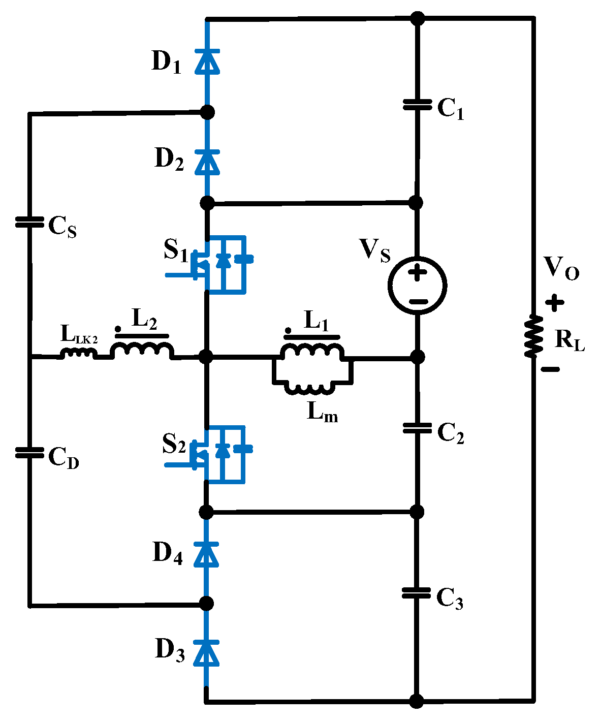
Figure 2.
Key waveforms of the proposed converter under CCM.
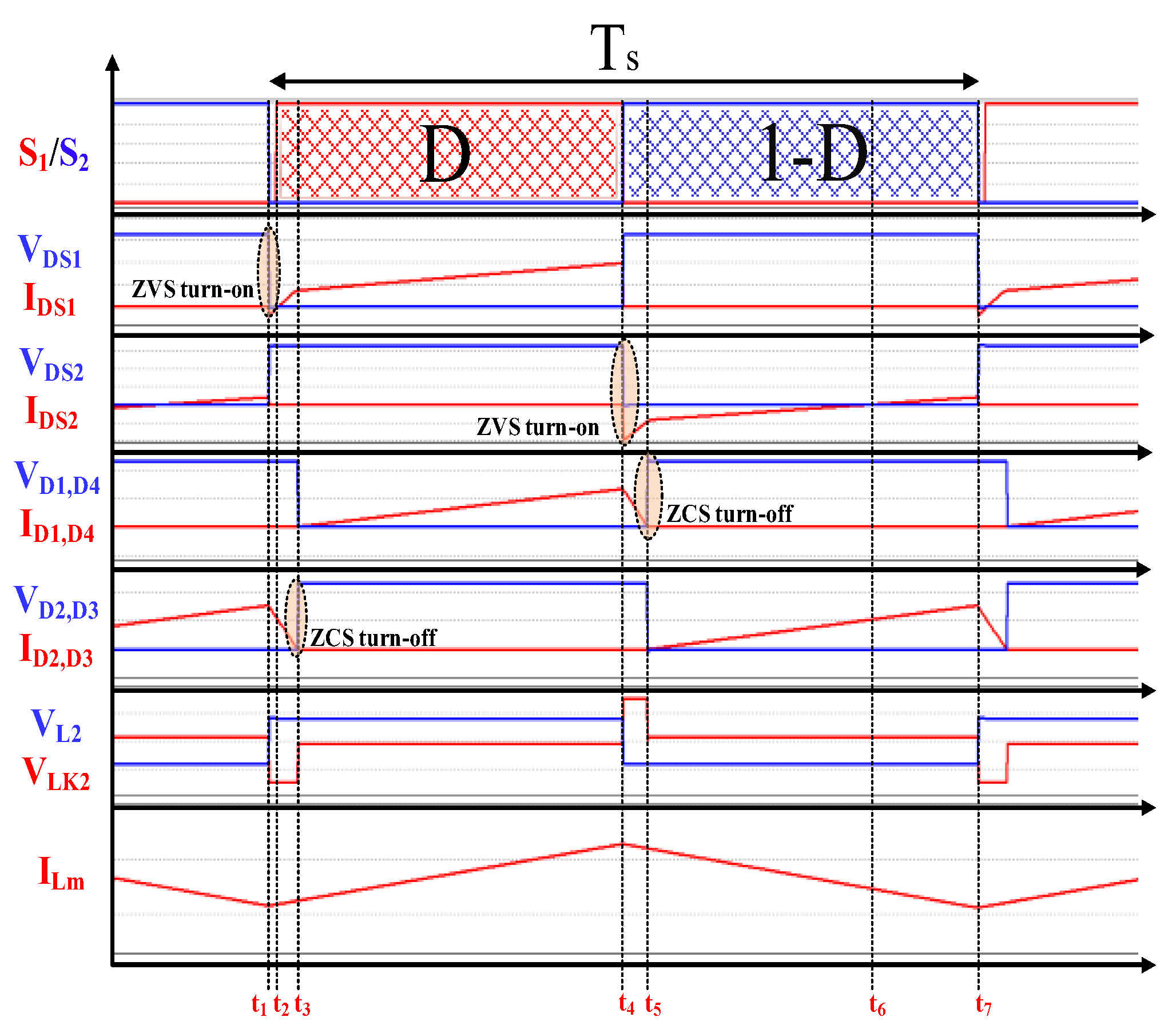
Figure 3.
Equivalent circuit of each mode of operation in the proposed converter under CCM: (a) Mode 1, (b) Mode 2, (c) Mode 3, (d) Mode 4, (e)Mode 5, (f) Mode 6.
Figure 3.
Equivalent circuit of each mode of operation in the proposed converter under CCM: (a) Mode 1, (b) Mode 2, (c) Mode 3, (d) Mode 4, (e)Mode 5, (f) Mode 6.
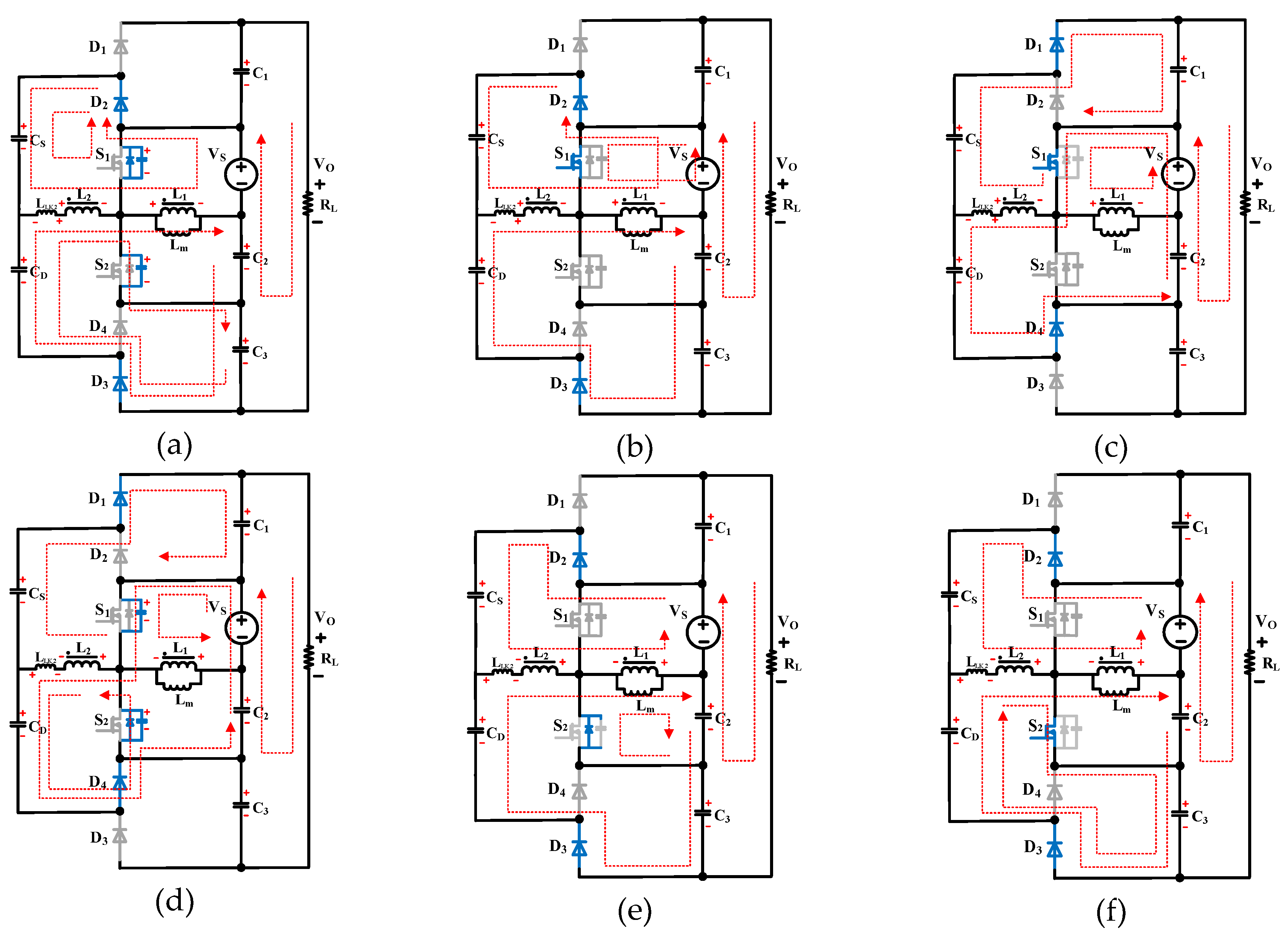
Figure 4.
Prototype of the proposed converter.
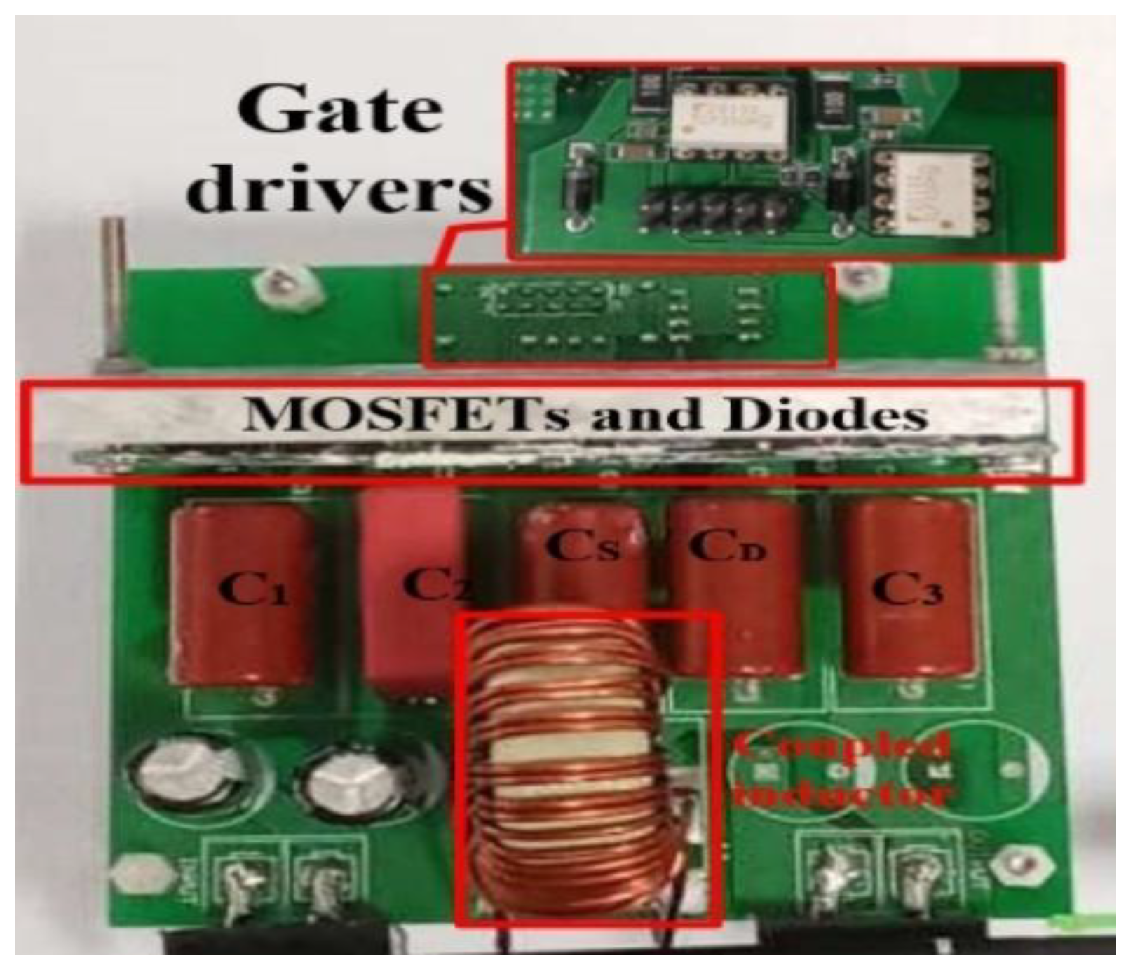
Figure 5.
Experimental waveforms of the prototype converter with 100% load: (a) MOSFET , (b) MOSFET , (c) Diodes and , (d) Diode and
Figure 5.
Experimental waveforms of the prototype converter with 100% load: (a) MOSFET , (b) MOSFET , (c) Diodes and , (d) Diode and
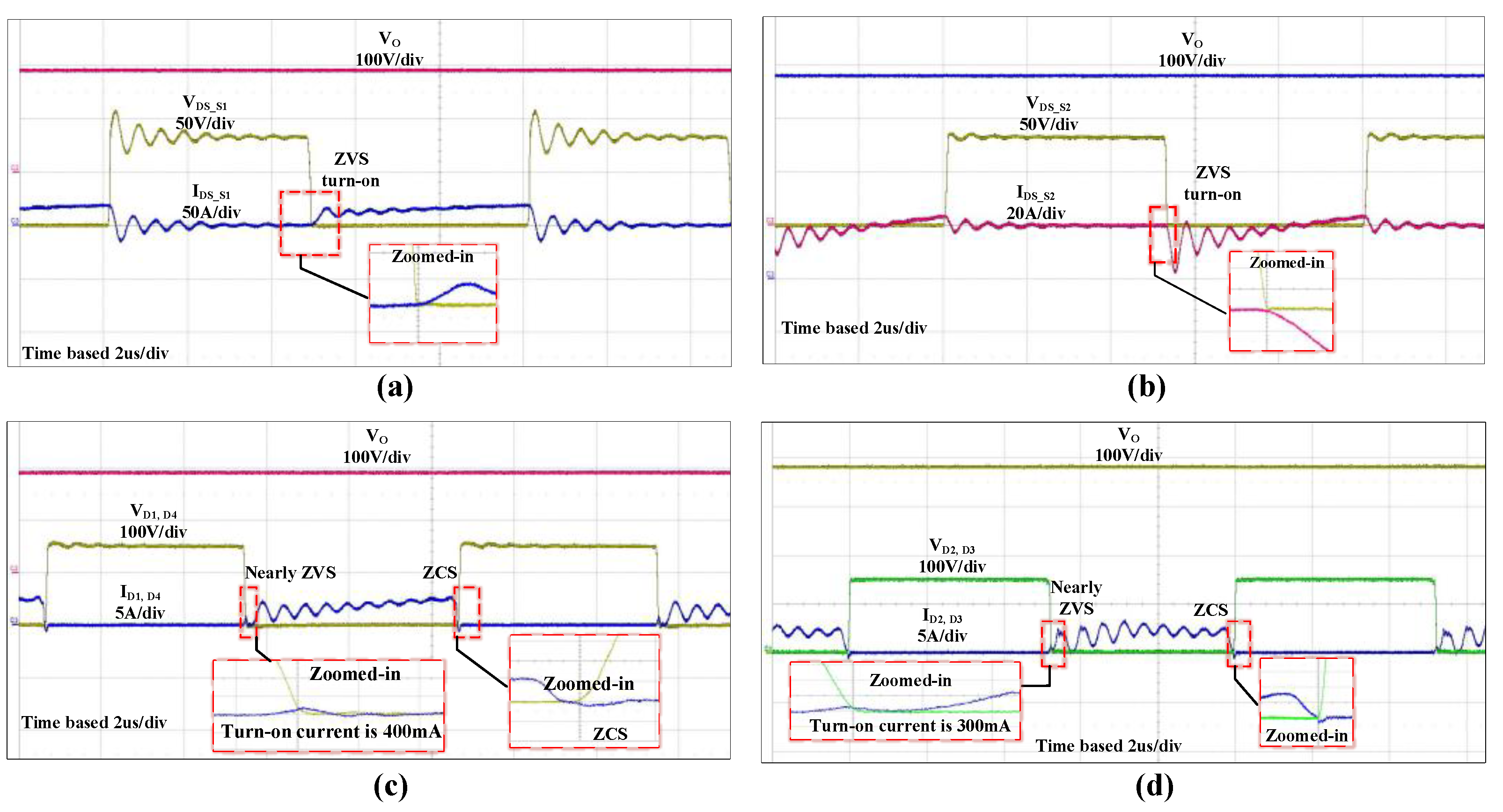
Figure 6.
Experimental waveforms of the proposed converter under light load conditions (20% load): (a) MOSFET , (b) MOSFET , (c) Diodes and , (d) Diode and
Figure 6.
Experimental waveforms of the proposed converter under light load conditions (20% load): (a) MOSFET , (b) MOSFET , (c) Diodes and , (d) Diode and
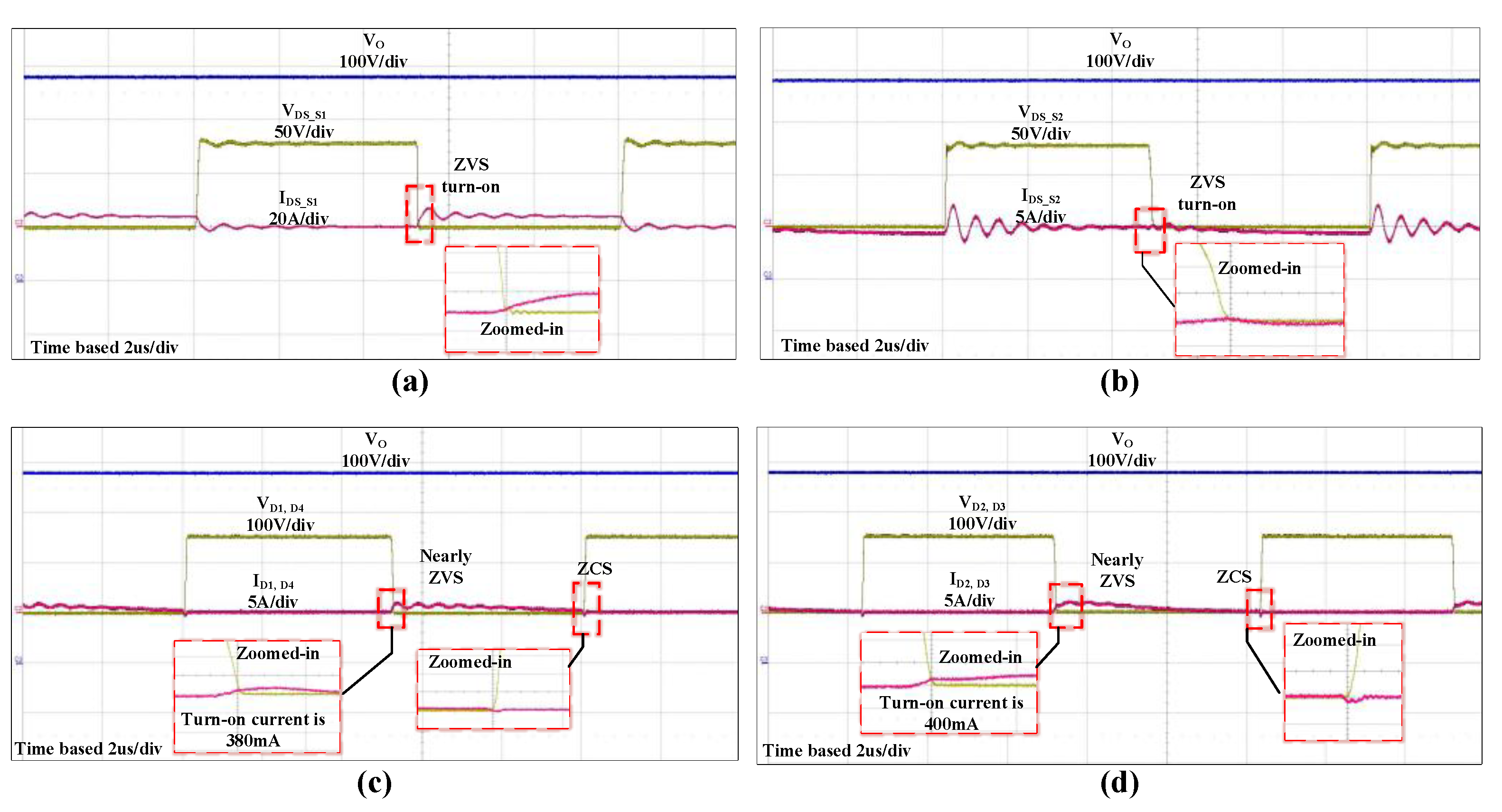
Figure 7.
(a) Experimental voltage waveforms of output capacitors, (b) Zoomed in waveforms of output capacitors voltage.
Figure 7.
(a) Experimental voltage waveforms of output capacitors, (b) Zoomed in waveforms of output capacitors voltage.
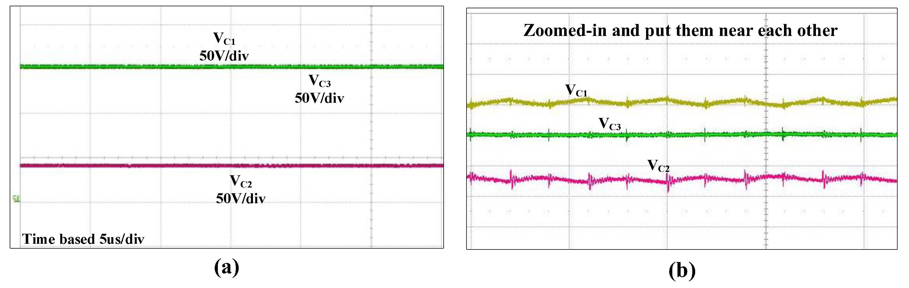
Figure 8.
(a) Experimental voltage waveforms of diodes and MOSFET , (b) zoomed-in voltage waveforms of diodes and MOSFET
Figure 8.
(a) Experimental voltage waveforms of diodes and MOSFET , (b) zoomed-in voltage waveforms of diodes and MOSFET
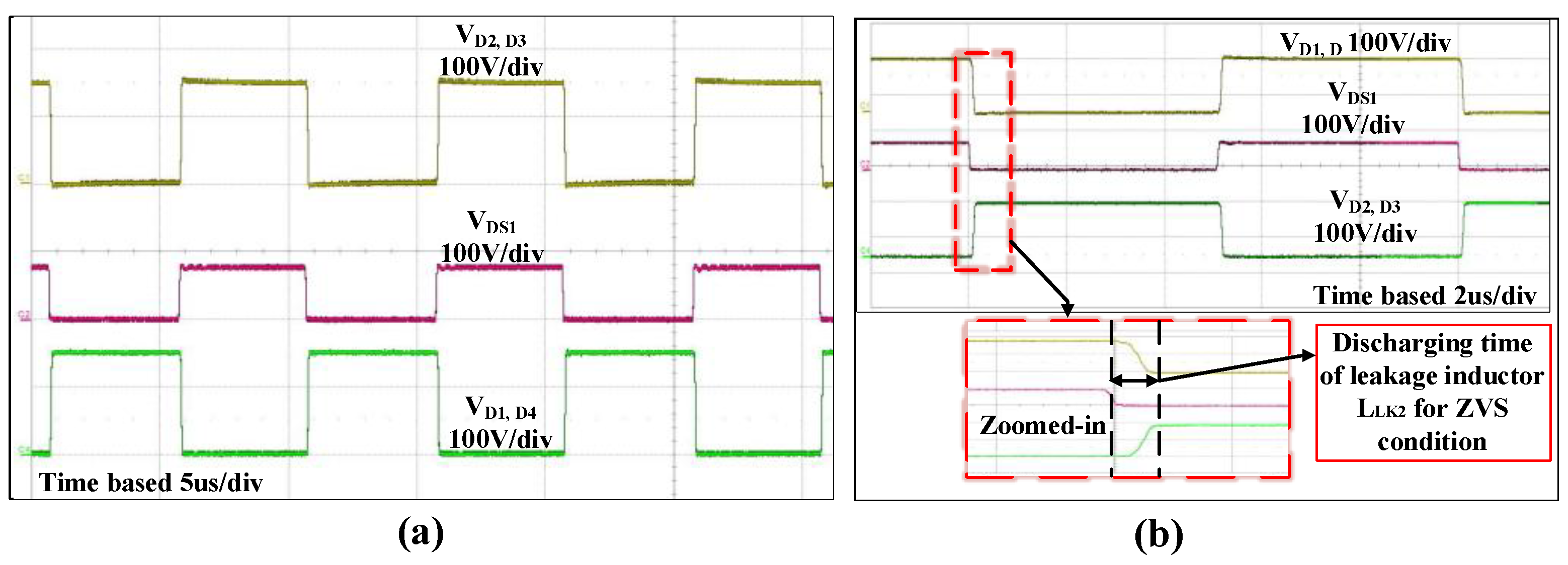
Figure 9.
Measured waveforms of the coupled inductor voltage and current.
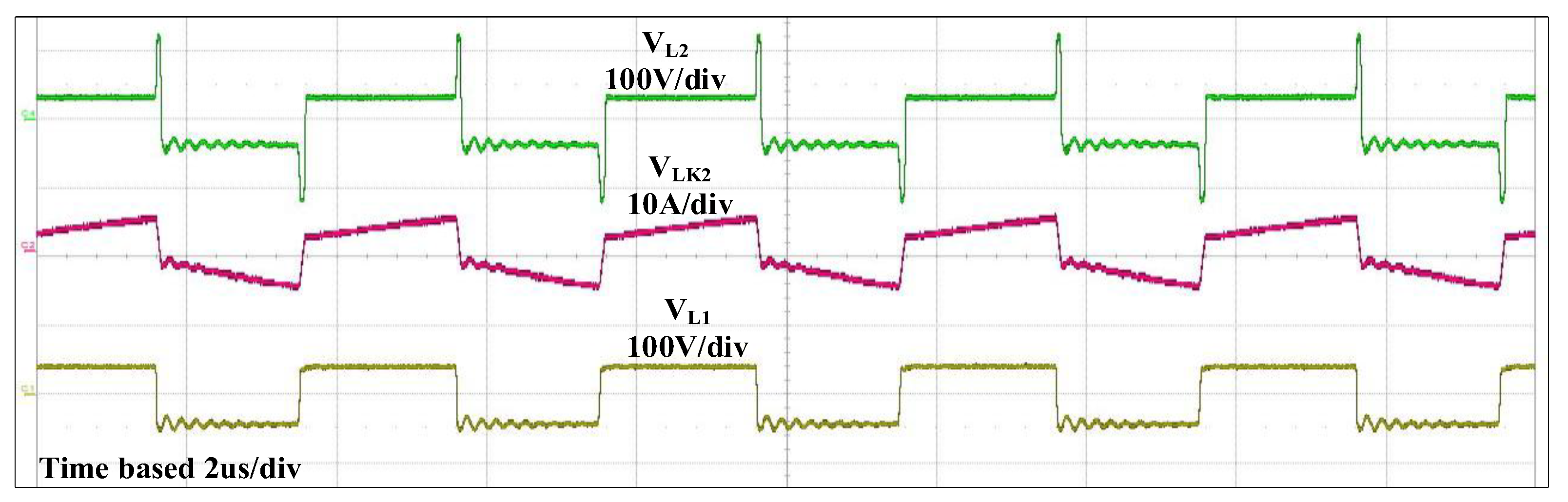
Figure 10.
Measured efficiency curve of proposed converter.
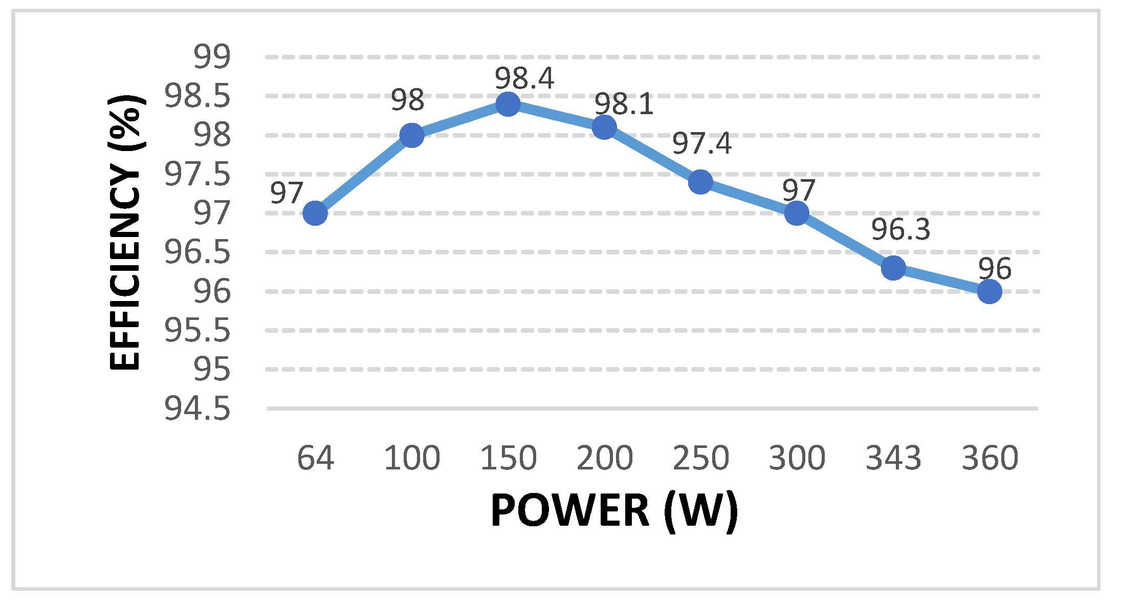
Figure 11.
(a) Voltage gain graph (b) Maximum voltage stress on diodes graph.
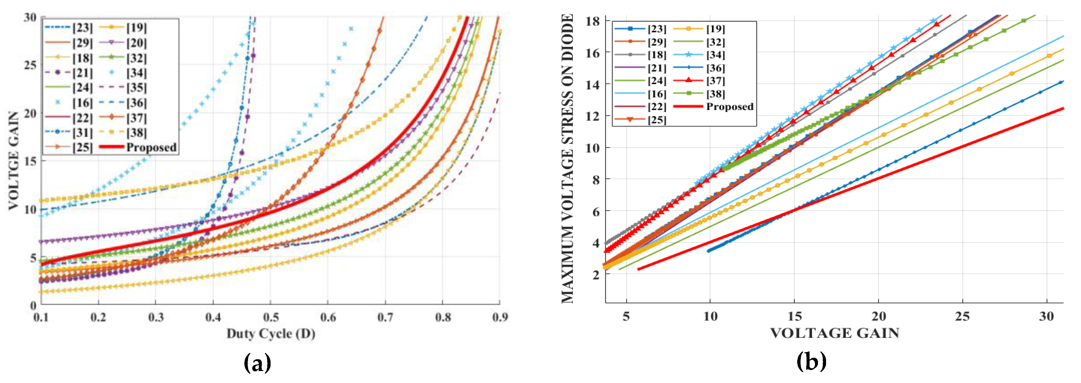

Table 1.
Specifications of the Proposed Converter.
| Parameter | Designator | Value |
|---|---|---|
| Input Voltage | 40 V | |
| Output voltage | 380 V | |
| Maximum Output voltage ripple | 0.8% | |
| Power | 360 W | |
| Switching frequency | 100 KHz |
Table 2.
Specifications of Components used in the Proposed Converter.
| Component | Part # | Specification |
|---|---|---|
| MOSFETs | IPP039N10N5 | 200 V/80 A |
| Diodes (-) | DSSK10-18A | 180 V/10A |
| Capacitors | 106MMR250K | 10uF/ 250 V |
| Turns-ratio of the coupled inductor | 17:18 | |
| Leakage inductance () | 4.5uH | |
| Primary winding inductance | 103uH | |
| Secondary winding inductance | 115uH |
Table 3.
Comparison of proposed converter with other existing topologies.
| Topology | Voltage gain |
Voltage stress on switches (Vs/Vin) | Maximum voltage stress on diodes (VDmax/Vin) | Maximum voltage stress on output capacitors (VCo/Vin) | S/D/CI/I/C/T | Efficiency |
|---|---|---|---|---|---|---|
| [23] | NI | 2/3/2/0/5/12 | 96.5% | |||
| [29] | 2/3/1/1/5/12 | 96.8% | ||||
| [18] | 1/2/1/1/3/8 | 94.1% | ||||
| [21] | 2/2/1/1/4/10 | 95.6% | ||||
| [24] | NI | 2/6/2/0/6/16 | 96.7% | |||
| [16](Figure 4a) | 1/6/1/1/5/14 | 94.4% | ||||
| [22] | 1/4/1/0/4/10 | 97.1% | ||||
| [31](Figure 6b) | NI | 1/4/1/1/5/12 | 95% | |||
| [25](Figure 4) | 1/3/1/0/3/8 | 96.4% | ||||
| [19] | 1/4/1/1/5/12 | 96.2% | ||||
| [20] | 1/8/1/0/8/18 | 97.6% | ||||
| [32] | 2/4/1/0/5/12 | 96.3% | ||||
| [34] | NI | 2/5/2/5/14 | 95.2% | |||
| [35] | 2/5/1/1/5/14 | 94.2% | ||||
| [36] | NI | 2/8/2/0/8/20 | 94.6% | |||
| [37] | 2/4/2/0/4/12 | 94.4% | ||||
| [38] | NI | 2/5/3/0/5/15 | 95.96% | |||
| Proposed converter | (11) | (10d) | (10d) | 2/4/2/0/5/13 | 98.4% |
With S/D/CI/I/C/T: Switch/Diode/Coupled Inductor/Single Inductor/Capacitor/Total, N: turns ratio of coupled inductor, NI: No Information.
Disclaimer/Publisher’s Note: The statements, opinions and data contained in all publications are solely those of the individual author(s) and contributor(s) and not of MDPI and/or the editor(s). MDPI and/or the editor(s) disclaim responsibility for any injury to people or property resulting from any ideas, methods, instructions or products referred to in the content. |
© 2025 by the authors. Licensee MDPI, Basel, Switzerland. This article is an open access article distributed under the terms and conditions of the Creative Commons Attribution (CC BY) license (http://creativecommons.org/licenses/by/4.0/).
Copyright: This open access article is published under a Creative Commons CC BY 4.0 license, which permit the free download, distribution, and reuse, provided that the author and preprint are cited in any reuse.


