1. Introduction
Among multiple patterning techniques, LELE stands as an essential practical method for overcoming the resolution limitations of 193nm lithography [
1]. It enables the fabrication of high-density patterns with sub-40nm half-pitch by decomposing the original design layout into two or more complementary mask sets. These masks are then used in multiple sequential litho-etch cycles, effectively surpassing the resolution limits of single-exposure DUV lithography without requiring Extreme Ultraviolet (EUV)-based processes.
The core principle of LELE involves decomposing complex patterns and realizing them through multiple cycles of exposure and etch, though this comes at the cost of demanding overlay control requirements and increased process complexity [
2,
3,
4]. However, the resist and etch models commonly used in the industry are only capable of simulating the patterns manifested on the wafer after a single exposure and etch process. Up to now, research on composite model that accurately describe the complete dual litho-etch process has not yet been reported. The inter-LE-cycle coupling makes it extremely difficult to accurately simulate the complete LELE process and predict the final wafer contour.
To address this limitation, we first turned to Scanning Electron Microscope (SEM) contour analysis-a metrology method uniquely suited to characterize pattern variability beyond simple Critical Dimensions (CD) measurements [
5]. Unlike CD gauges, which only quantify linear dimensions, SEM contours capture the full 2D shape of patterns. In this work, we extracted high-fidelity SEM contours at key LELE steps: LE1 ADI, LE1 AEI, LE2 ADI, and LE2 AEI. These contours serve as the foundational data for model calibration and validation, as they capture the precise pattern evolution across both LE cycles.
The key innovation of this work lies in integrating these SEM contour data with AI. Traditional modeling frameworks, which rely solely on physical terms, cannot fully resolve the complex, non-linear interactions between LE1 and LE2. By embedding small-scale neural networks (dubbed AI-Assisted Flexible Terms, AAFT) into the modeling workflow, we developed an AI-assisted composite etch model that explicitly captures the coupling between the two LE cycles. This model not only overcomes the limitations of single-cycle models but also achieves what was previously unfeasible: directly outputting the final post-LELE etch contour.
In summary, this work establishes a new paradigm for LELE process simulation. By combining SEM contour metrology (for high-quality input data) and AATF (for resolving inter-LE interactions and enhancing model fitting ability), we bridge the long-standing gap in full-LELE simulation. The resulting model enables not only accurate prediction of the final etched contour but also the early detection of AEI hotspots via ERC. Importantly, this workflow can be extended to more complex MPT scenarios, such as SARP combined with Cut processes.
2. Materials and Methods
2.1. Process Flow
This case study presents the metal layer patterning flow using LELE process of ArF-immersion, and Numerical Aperture (NA) is 1.35, mask type is opaque MoSi on glass(OMOG), with customer illumination, sector(X-Y) TE-polarized, and negative-tone develop(NTD) resist process.
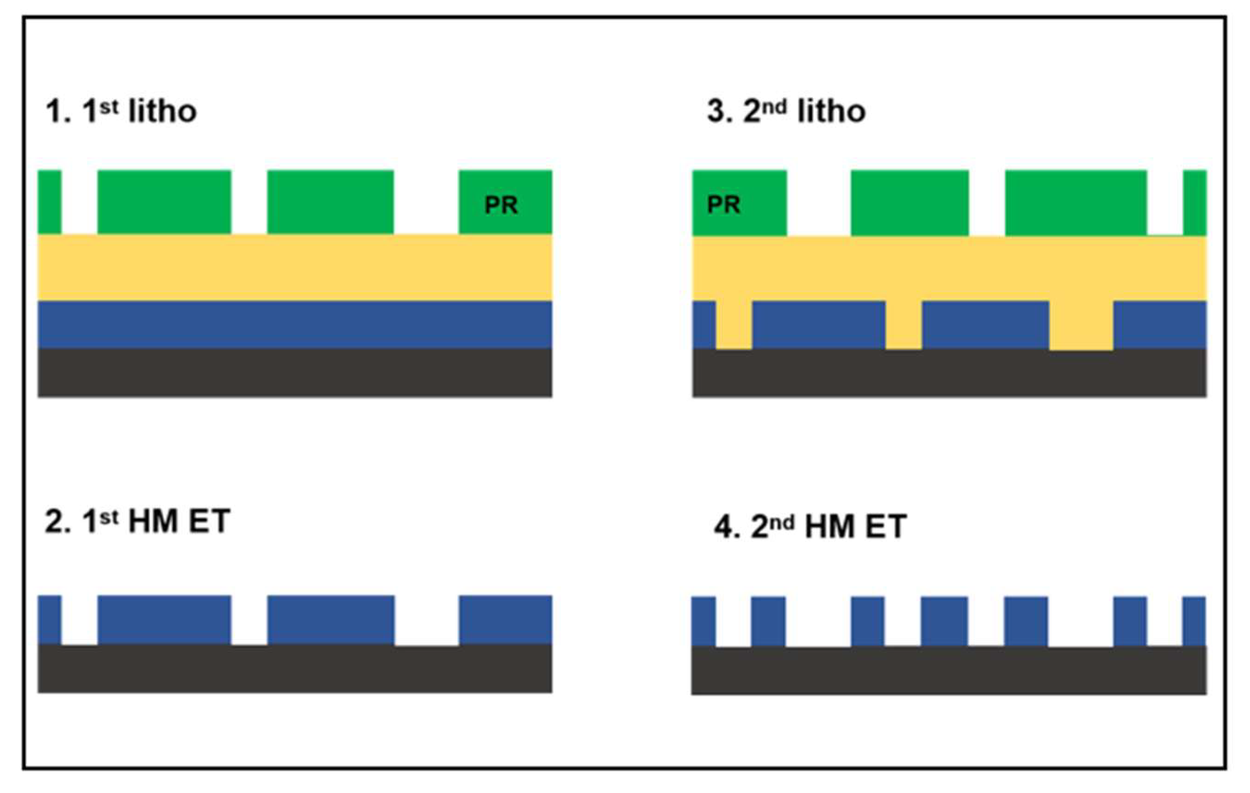
Pattern transfer flow as illustrated in
Figure 1. The LELE process comprises two steps: LE1 and LE2, which refer to the first and second litho-etch processes, respectively. LE1 is identical to a single litho-etch process; the challenge lies not in this step itself, but in the coupled effects between LE1 and LE2. Once the LE1 pattern has been transferred onto the hard mask, it forms an uneven incoming layer that influences both the exposure and etch process of LE2. Under these conditions, LE2 behaves differently compared to a single litho-etch process, resulting in a discrepancy between the LE2 wafer CD and the design CD. This deviation is referred to as CD variation. Additionally, during the strip step for photoresist removal in LE2, the process may interact with the LE1 pattern on the hard mask, leading to LE1 CD loss. Both LE2 CD variation and LE1 CD loss are undesirable from a design perspective, which probably lead to CD out of spec. In severe cases, this may lead to defects such as pinch or bridge. Covering these potential defects using traditional rule-based bias table methods is highly challenging. A more comprehensive approach involves using an LELE etch model to simulate the final LELE contour, followed by performing ERC checks.
2.2. Data Collection
Hitachi CD-SEM CG6300 was utilized for image generation and CD measurements, coupled with the DG-A software for contour extraction. Contours of test patterns at identical locations on both LE1 and LE2 were extracted, and point gauges were generated along the normal direction of the ADI/AEI contours for corresponding model calibration and validation. Among these, about 2800 gauges were used for model calibration, and 1200 gauges were reserved for validation.
2.3. Model Building
Due to the complex physical and chemical effects involved in etch process, achieving high model accuracy solely through traditional terms is challenging [
6,
7,
8,
9,
10]. With the rapid development of AI, there have been recent reports on utilizing AI algorithms to improve the accuracy of etch models [
11,
12]. Notably, the PanGen, a computational lithography product of DJEL (DONGFANG JINGYUAN ELECTRON CO., LTD), is entirely developed based on a hybrid Graphics Processing Unit (CPU)+Central Processing Unit (GPU) supercomputing architecture and Compute Unified Device Architecture (CUDA). It operates in the same computational environment as AI frameworks, enabling seamless integration of AI programs into the core functions of computational lithography. This inherent design allows PanGen to more effectively capitalize on the rapid advancements in AI technology, combining powerful AI algorithms with domain-specific expertise in computational lithography to deliver more efficient and intelligent solutions.
To enhance etch model accuracy, we have innovatively introduced small-scale neural networks as supplementary terms into the existing modeling framework-referred to as AAFT (
Figure 2). Powered by AI engines, AAFT significantly enhance the model fitting capability, leading to significant improvements in accuracy, particularly for 2D patterns. To mitigate overfitting risks: 1. AAFT are combined with explicitly physically traditional terms during model calibration; 2. Massive amounts of SEM contour datasets. This dual approach effectively reduces model overfitting, ensuring robust generalization capability alongside enhanced fitting performance.
The composite model for LELE process is composed of four sub-models, including the LE1 ADI/AEI model and the LE2 ADI/AEI model. For the ADI modeling of LE1 and LE2, the most widely used and mature photoresist modeling process can be followed. The LE1 AEI model, which is a single-etch model, can be effectively constructed using the aforementioned AI-assisted SEM contour-based modeling flow.
The composite nature of the model is reflected in the mutual coupling of inputs and outputs among the four sub-models. Specifically, the input to the LE1 ADI model is the LE1 aerial image. After being processed through relevant terms, it outputs the LE1 resist contour, which then serves as an input for calibrating the LE1 AEI model after being transform an image internally. Subsequent term processing yields the M01 etch contour, which can further be used as part of the input for the LE2 AEI model.
The main challenge in building the LELE composite model lies in the L2 AEI model since the interaction between LE1 and LE2. This study innovatively integrates the LE1 etch contour and the LE2 resist contour to generate a comb contour as one input channel. Meanwhile, the LE1 etch contour and the LE2 resist contour are also used as two additional independent input channels, resulting in a total of three input channels. These three channels are processed through their respective terms. Using the LE2 wafer AEI contour which is also the LELE final contour as the training label, the solver under AI framework is employed for iterative optimization to ultimately obtain a model with the minimal possible Root Mean Square error (RMS).
3. Results and Discussion
A direct comparison between the model’s calibration and validation results provides a straightforward indication of potential overfitting. The error of the composite model can be represented by the RMS metric, as detailed in
Table 1, which summarizes the calibration and validation results of both the ADI and AEI models for layer 1 and layer 2. As shown in
Table 1, the RMS for both calibration and validation are comparable across all four models, indicating a minimal risk of overfitting.
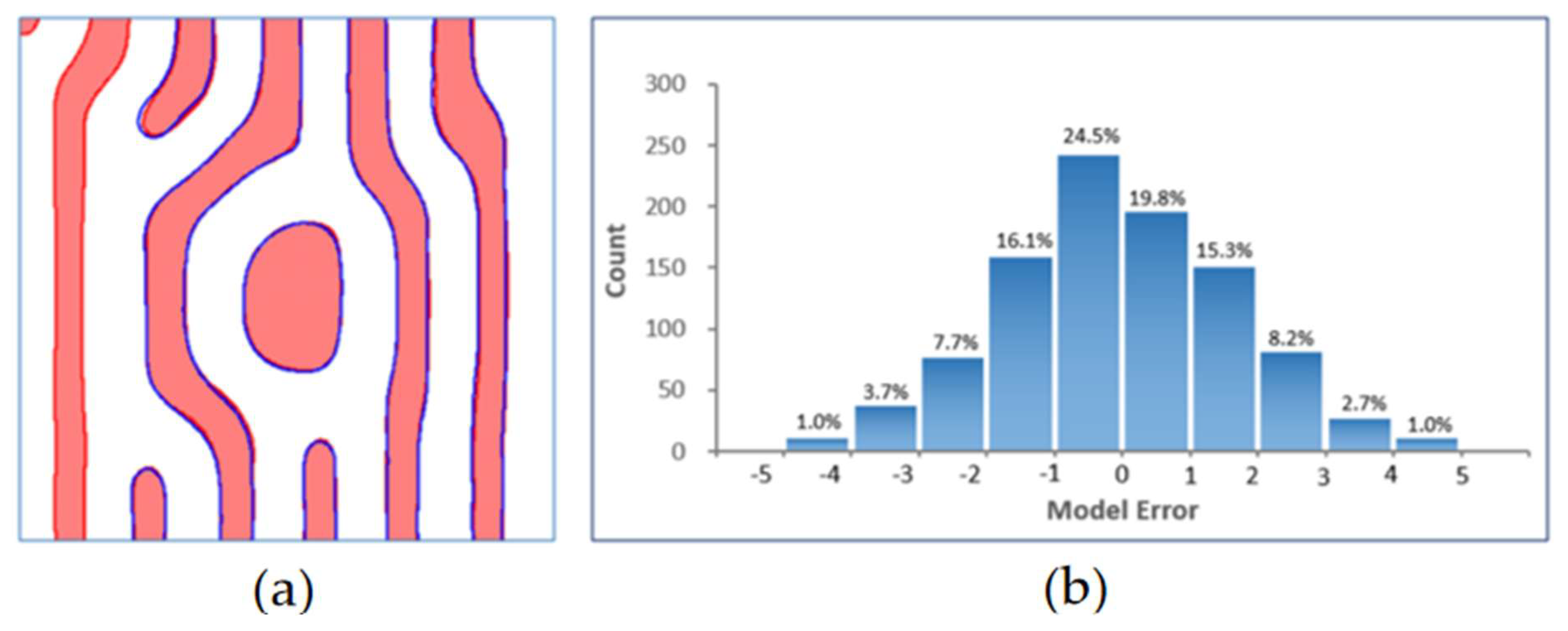
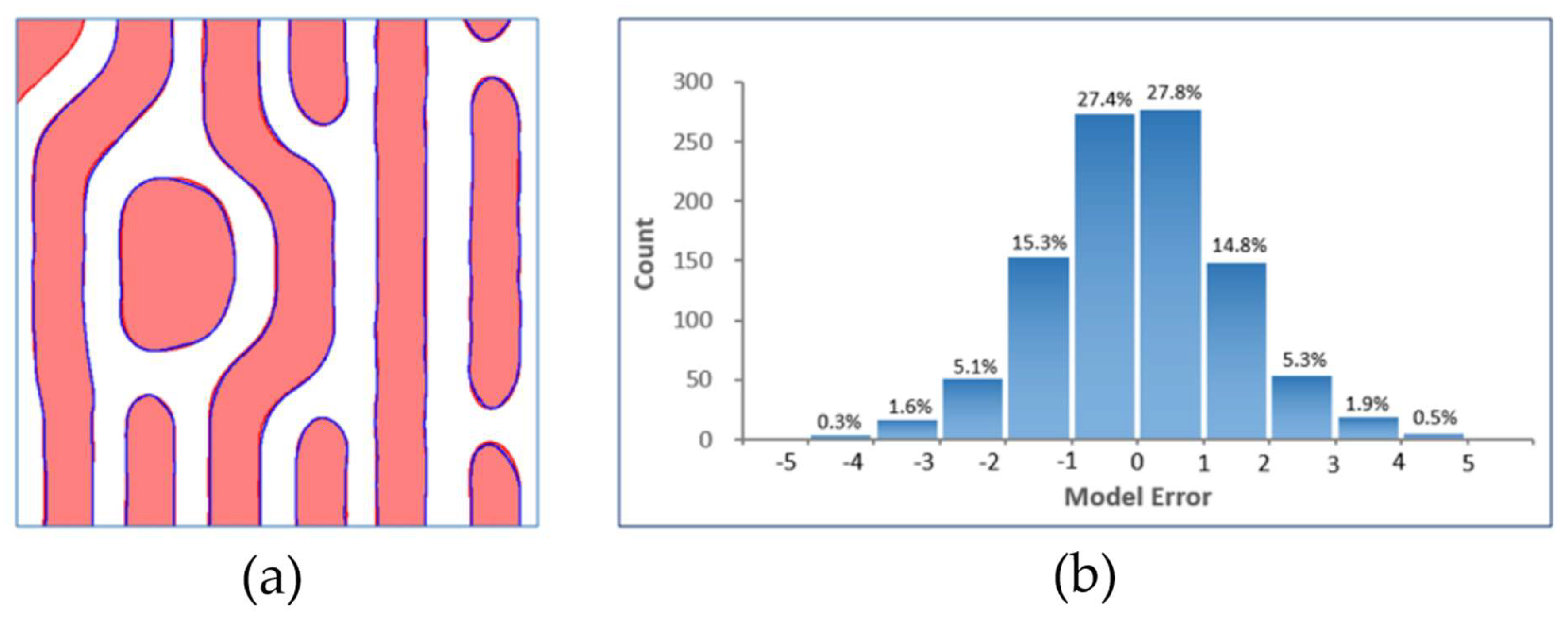
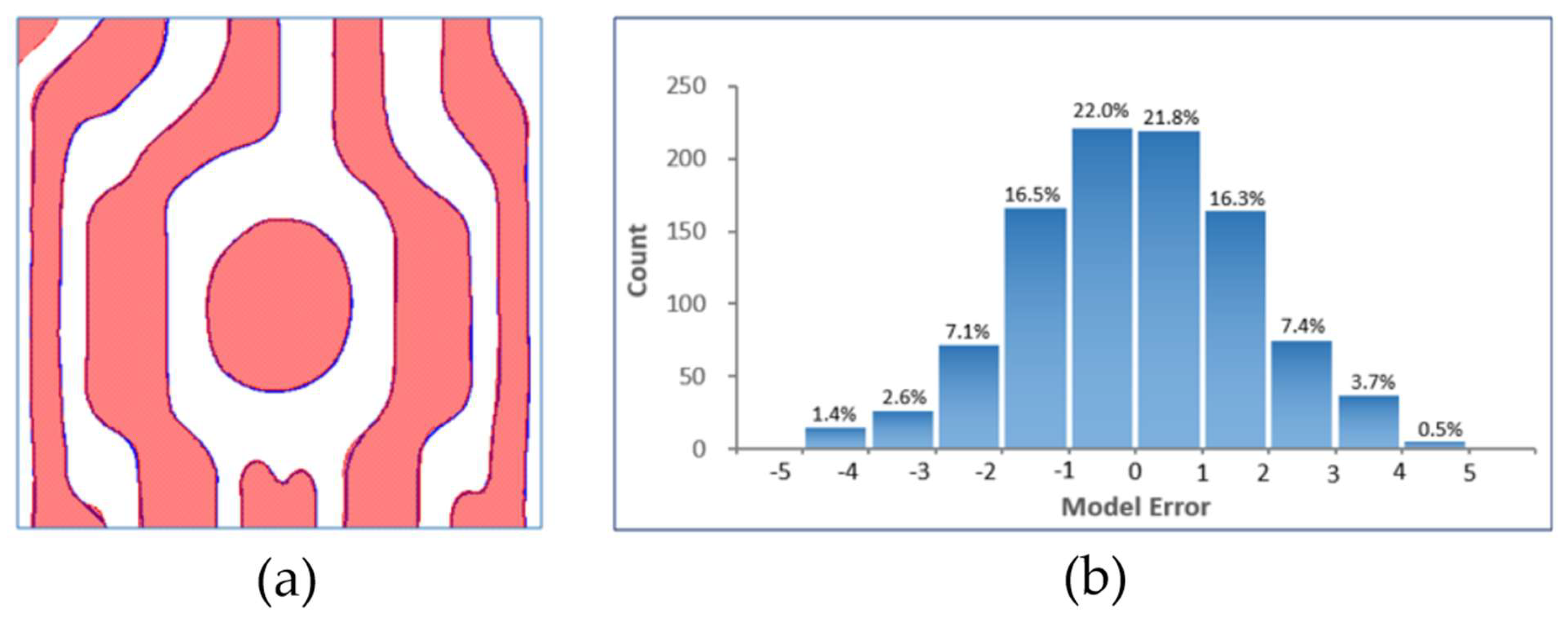
Figure 3,
Figure 4,
Figure 5,
Figure 6 present a comparative analysis of the contours extracted from ADI and AEI images at identical locations on the wafer alongside the corresponding simulated contours generated by the models, along with their respective model error distributions. It can be observed that all four models exhibit reasonable error ranges and distributions. Specifically, approximately 80% of the ADI model errors for both LE1 and LE2 fall within ±2 nm, while about 50% are within ±1 nm. Similarly, for the AEI models, nearly 75% of the errors for LE1 and LE2 are within ±2 nm, and approximately 42% are within ±1 nm. Furthermore, the point gauge’s errors exhibiting >2 nm are predominantly located at pattern corners or line ends. Based on the above analysis, the composite model developed for the LELE process demonstrates excellent agreement between simulated contours and experimentally extracted wafer contours, meeting all required accuracy specifications without exhibiting signs of overfitting.
4. Conclusions
This paper has presented a comprehensive AI-assisted and contour-based methodology for modeling the complex Litho-Etch-Litho-Etch (LELE) dual-patterning process. The results demonstrate that the calibrated models for all four stages (LE1 ADI, LE1 AEI, LE2 ADI, LE2 AEI or final LELE) show excellent agreement between simulated and extracted wafer contours. The RMS errors for calibration and validation are comparable across all models, indicating robust performance without overfitting. Furthermore, error analysis confirms that the majority of errors are within acceptable limits (±2 nm), with larger discrepancies predominantly occurring at challenging pattern features like corners and line ends.
In conclusion, the integrated model proves to be highly reliable for key computational lithography tasks: retargeting the design layout to ADI targets by compensating for etch bias and performing mask correction based on the ADI targets. This work provides a viable and accurate strategy for OPC model calibration in MPT, which is critical for ensuring high yield at advanced technology nodes.
5. Outlook and Future Work
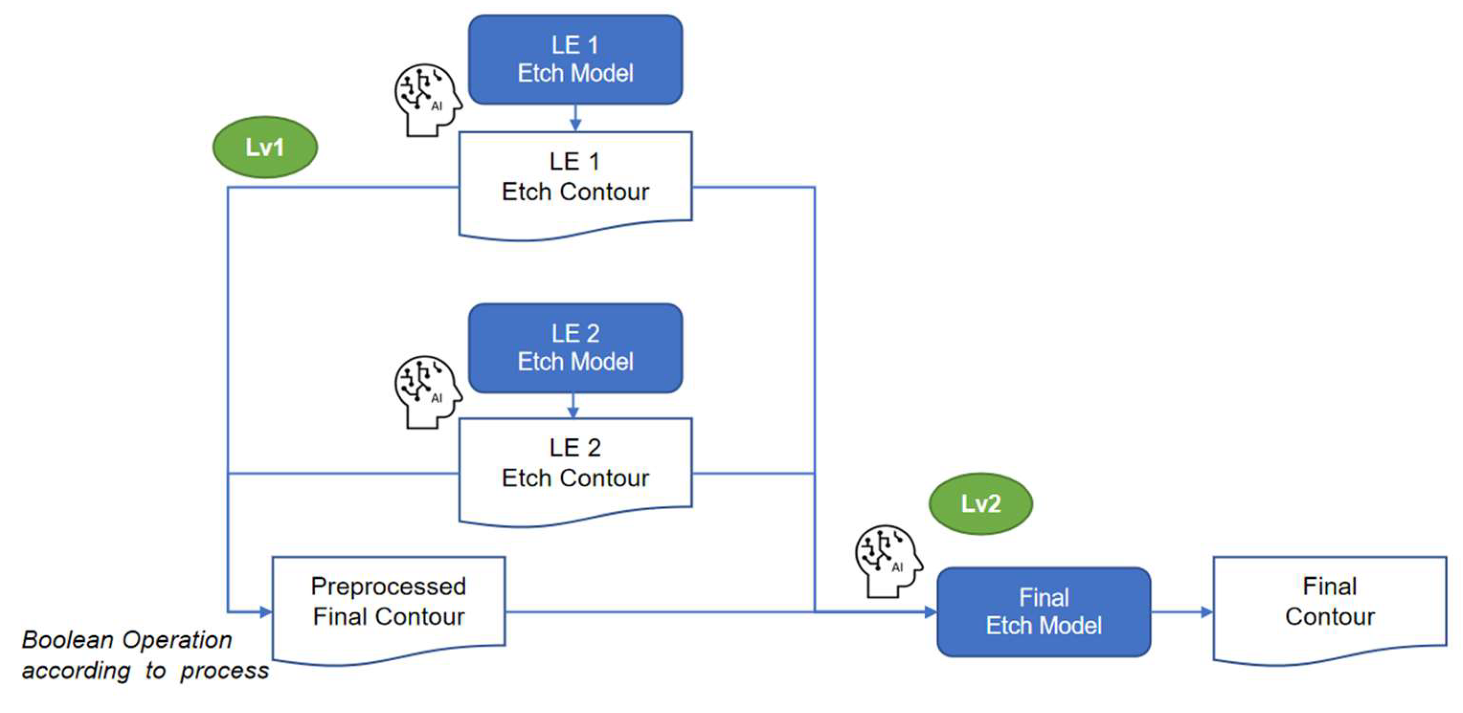
For future work, on one hand, conceptually, the current LELE modeling flow can be reconstructed into a more elegant structure with three sub-etch models arranged in two levels-this breaks the existing LE2 etch model into two separate steps, as illustrated in
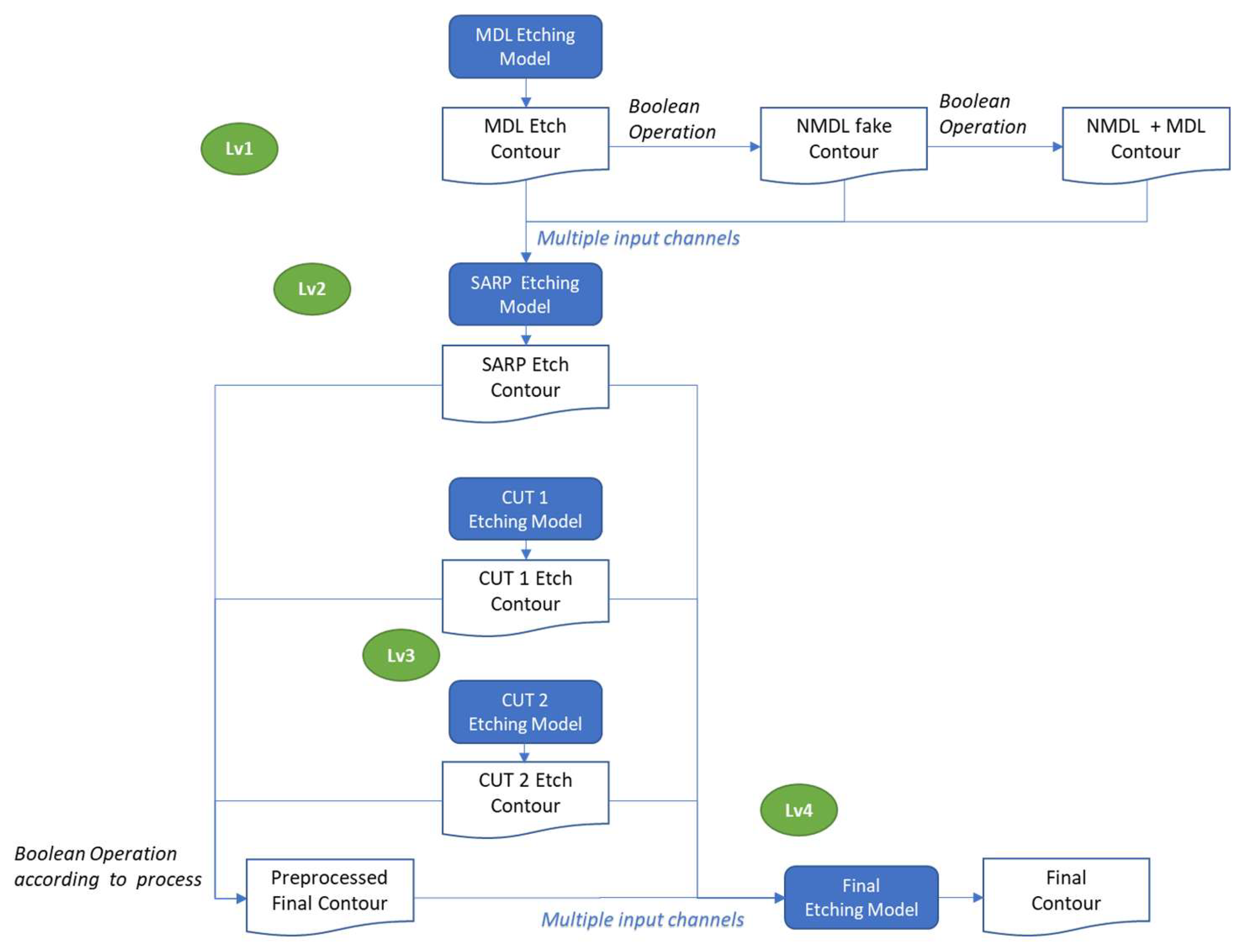
Figure 7. Leveraging the same methodology, this composite modeling approach can be extended to more complex patterning schemes, such as SARP+Cut process(shown in
Figure 8), which involves five sub-models organized in four levels.
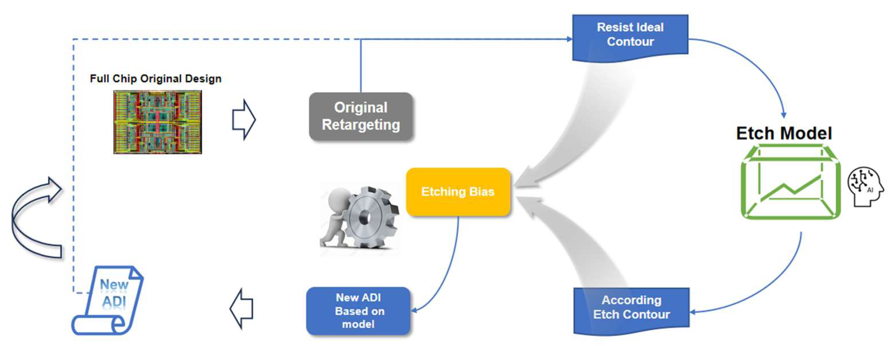
On the other hand, compared to traditional bias tables, the accurate etch model proposed in this work paves the way for developing an Auto Retargeting (ART) solution with higher accuracy and reduced labor costs.
Figure 9 presents the ART flow. The starting point for ART is the set of segments generated by the original bias table-based retargeting process. Control points are placed on these segments to quantify the discrepancy between the resist model contour and the etch model contour. Fundamentally, this approach mirrors the method used in OPC-where control points are placed on segments to measure the Edge Placement Error (EPE) between the resist model contour and either the ADI target or the ideal ADI contour.
Within the ART workflow, the ideal ADI contour is first fed as input into the etch model, which then generates the corresponding etch contour. The difference between these two contours (ideal ADI vs. generated etch contour) is calculated to quantify the etch bias. This bias value is subsequently used to update the initial ADI target-originally derived from traditional bias tables. Following one iteration, a revised ADI target is generated, which in turn yields an updated ideal contour. The iteration process is repeated until the newly computed etch bias converges closely with the pre-existing bias values, which can provide a much more accurate ADI target compared to original one obtained from bias table. Notably, this multi-iteration ADI target correction process-driven by the etch model-is analogous to mask optimization in OPC, which relies on a resist model. However, it represents a distinctly new scenario: in this workflow, the correction focuses on the ADI target itself, rather than the mask.
To conclude, the etch model’s ability to extend to complex MPTs (such as self-aligned patterning) and the ART flow together enhance the practical value of the proposed framework-thereby providing a reliable, scalable foundation for computational lithography in advanced semiconductor nodes, where high-precision patterning are of paramount importance.
Author Contributions
Conceptualization, W.L., C.H and S.Z; Methodology, S.Z.; Validation, Y.G., F.Z. and D.S.; Investigation, Y.G., F.Z; Resources, C.H., S.Z.; Data curation, Y.G.; Writing—original draft preparation, Y.G., D.S.; Writing—review and editing, C.H., S.Z.; Project administration, C.H., S.Z.; All authors have read and agreed to the published version of the manuscript. The authors from [DJEL (DONGFANG JINGYUAN ELECTRON CO., LTD)] specifically conceived, developed, and interpreted the [AI-assisted composite model for MPT and auto-retargeting] methodology presented in this manuscript.
Data Availability Statement
The original contributions presented in this study are included in the article. Further inquiries can be directed to the corresponding author.
Acknowledgments
This work was supported by Fujian JinHua Integrated Circuit., LTD. We acknowledge Fujian Jinhua Integrated Circuit Co., Ltd. for the collaborative partnership and for providing the data.
Conflicts of Interest
The authors declare no conflict of interest.
Author Note
Data Source: This study and the research [Devin.Sima, WenzhangLi. YingXiong.Guo,T.H.Ying, Yanbin.Gong, Fengsheng.Zhao, Shengrui.Zhang, C.M.Hu, A composite model for LELE process, manuscript submitted for IWAPS] are based on the same dataset from a joint project, used for independent analysis with mutual agreement.
References
- Zhou, W.; Wei, F.; Zhang, Y.; Zhu, J.; Hu, C.; Cho, K.; Corradi, A.; Pao, K.; Jain, V.; Elmalk, A.; Raghunathan, S.; Hunsche, S.; Zhu, R.; Chen, S.; Lin, L.; Liang, L.; Liu, L. Contour-based metrology for assessment of edge placement error and its decomposition into global/local CD uniformity and LELE intralayer overlay, Proc. SPIE 2021, 11611. [Google Scholar]
- Tseng, S.; Chen, A. Process capability comparison between LELE DPT and spacer for NAND flash 32nm and below. Proc. SPIE 7140, Lithography Asia 2008, 714035. [Google Scholar]
- Peng, F.; Sun, C.; Hui Wan, H.; Gui, C. An Improved 3D OPC Method for the Fabrication of High-Fidelity Micro Fresnel Lenses. Micromachines 2023, 14, 2220. [Google Scholar] [CrossRef] [PubMed]
- Fleming, A.; Wills, A.; Routley, B. Exposure optimization in scanning laser lithography. IEEE Potentials 2016, 35, 33–39. [Google Scholar] [CrossRef]
- Hibino, D.; Shindo, H.; Hojyo, Y. “The assessment of the impact of mask pattern shape variation on the OPC-modeling by using SEM-Contours from wafer and mask,” Proc. SPIE 8166, W. Maurer and F. E. Abboud, Eds., 1–9 (2011).
- Weisbucha, F.; Luticha, A.; Schatz, J. Pattern sampling for etch model calibration. Proc. of SPIE Vol. 10446.
- Lee, J.; Heo, Y.; Lee, R.; Kima, S.; Honga, J.; Kooa, K.; Yima, C.; Kima, J.; Lee, S.; Kima, J.; Kima, D.; Yanga, S.; Jeonga, S. A novel approach to etch-process-aware intensive layout retarget. Proc. of SPIE Vol. 12499.
- Weisbuch, F.; Lutich, A.; Schatz, J. Introducing etch kernels for efficient pattern sampling and etch bias prediction. J. Micro/Nanolith. MEMS MOEMS Vol. 013505.
- Schatza, J.; Weisbucha, F.; Luticha, A. Contour based etch modeling enablement: from pattern selection to final verification. Proc. of SPIE Vol. 10446.
- Hu, L.; Jung, S.; Li, J.; Kim, Y.; Bar, Y.; Lobb, G.; Liang, J.; Ogino, A.; John, S.; Bailey, T. Multi-Layer VEB Modeling: Capturing Interlayer Etch Process Effects for Multi-Patterning Process. Proc. of SPIE Vol. 9780.
- Kim, Y.; Jung, S.; Kwak, D.; Liubich, V.; Fenger, G. Predictable Etch Model Using Machine Learning. Proc. of SPIE Vol. 10961.
- Salamaa, M.; Hamouda, A. Efficient Etch Bias Compensation Techniques for Accurate On wafer Patterning. Proc. of SPIE Vol. 9427.
|
Disclaimer/Publisher’s Note: The statements, opinions and data contained in all publications are solely those of the individual author(s) and contributor(s) and not of MDPI and/or the editor(s). MDPI and/or the editor(s) disclaim responsibility for any injury to people or property resulting from any ideas, methods, instructions or products referred to in the content. |
© 2025 by the authors. Licensee MDPI, Basel, Switzerland. This article is an open access article distributed under the terms and conditions of the Creative Commons Attribution (CC BY) license (http://creativecommons.org/licenses/by/4.0/).