
Submitted:
02 March 2025
Posted:
03 March 2025
You are already at the latest version
Abstract
Wet etching is the mainstream fabrication method for single-bar quantum cascade lasers (QCLs). Different etching solutions result in varying etching effects on III-V semiconductor materials. In this study, an efficient and nearly ideal etching solution ratio was proposed for simultaneously etching both InP and GaInAs/AlInAs, and the surface chemical reactions induced by each component of the etching solution during the process were investigated. Using univariate and single-component experiments, coupled with various characterization techniques such as atomic force microscopy (AFM), stylus profilometer, X-ray photoelectron spectroscopy (XPS), and scanning electron microscopy (SEM), we found that the ratio of HBr to hydrogen peroxide significantly determines the etching rate, while the ratio of HCl to hydrogen peroxide affects the interface roughness. The aim of this study was to provide a comprehensive understanding of the effects of different etching solution components, thereby enhancing the understanding of the wet etching process for InP/GaInAs/AlInAs materials. These findings offer valuable insights for efficient QCL fabrication processes and contribute to the advancement of the field.
Keywords:
Quantum cascade laser (QCL)
; Wet etching
; InP/GaInAs/AlInAs
; Solution
1. Introduction
Quantum cascade lasers (QCLs), with their unique band structure design and intersubband transitions, have become key light sources in the mid-infrared (MIR) to terahertz (THz) spectral regions [1,2,3]. Their small size, potential for integration, narrow linewidth, and tunable wavelength make them indispensable in applications requiring precise molecular fingerprint detection [4,5,6]. However, challenges remain in achieving efficient operation with high output power and low threshold current density at room temperature [7,8]. The growth of QCL materials based on InP/GaInAs/AlInAs relies on molecular beam epitaxy (MBE) and metal-organic chemical vapor deposition (MOCVD), which, to some extent, can achieve material flattening during epitaxial growth. The precision and quality of the fabrication process are critical to the overall light emission efficiency. In QCL, the ridge waveguide structure confines light through raised strips (ridges) etched directly on the epitaxial wafer, using the refractive index contrast for lateral optical confinement. It enables efficient mode control in semiconductor lasers. The ridge waveguide structure of a quantum cascade laser can be fabricated using either dry etching or wet etching methods. Bewley et al. found that ridge waveguides fabricated using dry etching [9] may suffer from surface crystal damage, rough sidewalls, surface recombination, and current leakage, leading to higher threshold currents for the QCL. In contrast, ridge waveguides fabricated using wet etching yield smooth sidewalls.
In recent years, significant interest has been generated in the study of etching solutions for different systems [10,11,12,13,14,15]. However, challenges still exist, including unclear experimental mechanisms, weak etching modes, and a lack of understanding of the role of the etching solution components. Furthermore, many descriptions of wet etching processes are overly general and inconsistent. Among the previously reported etching systems for InP/GaInAs/AlInAs materials, commonly used etching solutions include HCl : HNO3 : H2O, HBr : HNO3 : H2O, and HBr : HCl : H2O2 : H2O. In the hydrochloric acid system, the HCl+HNO3+H2O etching solution has a strong oxidizing property, which is too aggressive for the AZ5214 (a positive-tone photoresist, MicroChemicals GmbH) photoresist used as a mask, leading to the collapse and dissolution of the photoresist during the etching process. Additionally, the surface morphology after etching is poor, making it unsuitable for device fabrication [16]. The hydrogen bromide-based etching solution does not corrode the AZ5214 photoresist, and the HBr + HNO3 + H2O solution produces a good surface morphology. However, it exhibits strong crystal orientation selectivity, requiring close monitoring of wafer orientation, which makes certain slanted cavity structures impractical [17]. In addition, this solution is typically used to etch the GaInAs/AlInAs active region and needs to be combined with an H3PO4 + HCl solution to etch the InP upper waveguide layer [18,19]. Moreover, this solution requires at least 24 hours of standing time after preparation, and HBr needs to be stored in the dark, which complicates the process and reduces device fabrication efficiency [20,21]. In contrast, the HBr + HCl + H2O2 + H2O etching solution neither corrodes the AZ5214 photoresist nor requires prolonged preparation time, while also enabling the simultaneous etching of InP/GaInAs/AlInAs in a single step.
This study comprehensively evaluates the optimal composition of etching solutions suitable for the InP/GaInAs/AlInAs system, based on HBr : HCl : H2O2 : H2O etching liquids, considering factors such as etching rate, surface roughness, and crystal orientation selectivity. The research delves into the role of different etching solution components in the etching process of various materials. This is of significant importance for a deeper understanding of the wet chemical etching characteristics of InP/GaInAs/AlInAs superlattice materials. The study investigates how changes in the etching solution composition can optimize the etching process, enabling precise control over the etching rate and surface roughness. These findings provide valuable guidance for the process fabrication of quantum cascade lasers in this system. Furthermore, examining the effects of each etching solution on different materials will contribute to a more comprehensive understanding of the interactions and properties between materials.
2. Materials and Methods
The samples used in this study are QCL full structures, as shown in Figure 1(a). All samples were grown on InP (100) substrates via solid-source molecular beam epitaxy (MBE). The growth process began at 440°C with the deposition of a 300 nm thick GaInAs buffer layer following substrate deoxidation. Subsequently, the substrate temperature was lowered to 420°C to grow the QCL active core region. The active core consists mainly of Ga0.31In0.69As/Al0.64In0.36As quantum wells paired with Ga0.47In0.53As/Al0.48In0.52As superlattices, with an overall thickness of approximately 1.8 μm. After the core region growth, a 180-200 nm thick GaInAs buffer layer was deposited to mitigate the effects of secondary epitaxy on the core region. The thickness of the upper waveguide layer of InP is around 2 μm.
The surface defects and roughness of the epitaxial wafer were characterized using a Park NX10 atomic force microscope (AFM). As shown in Figure 1(b), the sample surface exhibits excellent properties with a roughness of only 0.2 nm. The structural quality of the epitaxial layers was evaluated using a PANalytical X'Pert³ MRD high-resolution X-ray diffraction (HRXRD) system. Figure 1(c) presents the X-ray diffraction spectrum of the structure. The satellite peaks are clearly defined, exhibiting regular satellite peak spacing and a narrow full width at half maximum, with the 0th-order peak coinciding with the substrate peak. These features collectively indicate that the sample possesses outstanding crystal quality, resulting in a flat and strain-balanced surface, providing a solid foundation for subsequent process fabrication.
The etching experiments were conducted in a class 100 cleanroom, with the solution temperature maintained at a constant 25°C. Additionally, N₂ drying was employed to suppress surface oxidation and maintain uniform surface conditions. To investigate the effects of wet etching on the various material systems within the structure, we selected HBr (41%), HCl (45%), H2O2 (30%), and deionized water for the experiments. After thoroughly mixing the etching solutions, the mixtures were allowed to sit for one hour until their color changed from transparent to orange-red, allowing the Br- in HBr to be fully oxidized to Br2 before the experiment w initiated. To study the effects of each solution on the materials, etching was carried out using several different solutions, including BCHD (a mixture of hydrogen peroxide, HBr, HCl, and deionized water), BHD (a mixture of HBr, H2O2, and deionized water), CHD (a mixture of HCl, H2O2, and deionized water), and BCD (a mixture of HBr, HCl, and deionized water).

Table 1.
Abbreviations for the Different Etching Solution Compositions Designed in This Experiment.
| HBr (Hydrobromic acid) |
HCL (hydrochloric acid) |
H2O2 (Hydrogen Peroxide) |
DIW (Deionized water) |
|
|---|---|---|---|---|
| BCHD | Add | Add | Add | Add |
| BHD | Add | / | Add | Add |
| CHD | / | Add | Add | Add |
| BCD | Add | Add | / | Add |
The etching rates and surface roughness were accurately measured using a KLA Tencor P-17 desktop stylus profiler with a calibrated stylus force of 0.5 mN and a scanning speed of 0.1 mm/s to minimize surface deformation and a Non-contact mode of AFM. The solution compositions that resulted in similar etching rates for InP and GaInAs/AlInAs, along with lower surface roughness, were identified. The chemical states of the surface oxide layers for different etching solution compositions were studied using Scienta Omicron X-ray photoelectron spectroscopy (XPS). XPS measurements were conducted in a high-vacuum chamber equipped with an XPS system, which includes an Al X-ray source and a hemispherical electron energy analyzer (EA125). During the experiment, the electron emission angle was set to 63°, and the electron spot size on the X-ray anode was measured to be 1.5 mm × 2.5 mm. During the analysis, an Omicron system FS40 (charge neutralizer) was employed to compensate for any electron charging effects. The operating parameters of the charge neutralizer were: working energy 1V, emission current 100μA, and focusing voltage 300V. The XPS peaks were calibrated by aligning the C 1s peak at 284.8 eV. The interface of the samples after etching was characterized using the integrated SEM in a Raith Pioneer two-electron beam lithography system to evaluate the impact of the etching solution on the crystal orientation selectivity of the sample.
Results
3.1. The Role of Each Component in BCHD Solution
To investigate the effects of different components on the etching rate and surface roughness, the samples were treated with BCHD solutions of varying concentrations. The initial solution composition was set as 4 mL of HBr, 2 mL of HCl, 1 mL of H₂O₂, and 50 mL of DIW. Keeping other solution components constant, univariate experiments were carefully conducted by independently varying the concentrations of hydrogen bromide, hydrochloric acid, and hydrogen peroxide in each solution over discrete time intervals. Each experiment was repeated three times under identical conditions. The Figure 2 reported etch rates and roughness values represent mean ± standard deviation, with variations below 6% between trials.
As shown in Figure 2(a) and 2(c), it is clear that the etching rate is strongly positively correlated with the concentrations of HBr and H2O2. As the concentration of HBr increases, the etching rate rises sharply. In contrast, the effect of HCl on the etching rate is relatively minimal; even when the concentration of HCl increases by a factor of four, the etching rate remains around 0.6 μm/min, as shown in Figure 2(b). The concentration of H2O2 also significantly affects the etching rate; when the concentration is 1 mL or 1.5 mL, the curve stabilizes, and the etching rates are nearly identical. At concentrations of 0.5 mL and 2 mL, the etching rate shows a sharp decrease and increase, respectively. To achieve the best etching results with a smooth bottom surface and interface, AFM measurements were performed on the bottom surfaces of 12 groups of samples after etching and de-photoresist processing. We found that excessive H2O2 causes the bottom surface roughness to increase dramatically to 10 nm, which significantly affects the material quality. The effect of HCl showed a slight increasing trend in roughness with increasing concentration, but even when the concentration reached 4 mL, the roughness was only 3.2 nm. The relationship between HBr concentration and bottom surface roughness is nonlinear. The least impact on the bottom surface roughness occurred at concentrations of 4 mL and 5 mL, while at concentrations of 3 mL and 6 mL, the roughness was around 4 nm.
The wet etching process mainly consists of oxidation and decomposition. As shown in equation 1, in the BCHD solution, the orange-red solution formed after mixing and standing contains Br₂ as the core oxidizing agent. H2O2 assists in the oxidation of Br⁻ and participates in some of the oxidation reactions. Therefore, an excess of H2O2 and HBr leads to an oxidation rate that exceeds the dissolution rate, causing the accumulation of insoluble substances, which results in surface roughness [22]. Increased HBr concentration directly increases the Br₂ concentration, significantly accelerating the oxidation reaction rate. As a result, increases in both HBr and H2O2 concentrations lead to a noticeable increase in the etching rate. In contrast, the role of HCl in the etching solution is primarily to provide H⁺ ions, maintaining a strongly acidic environment. We speculate that, under such acidic conditions, the oxidation capability of H2O2 may not be sufficient to oxidize Cl⁻, while it is more likely to oxidize Br⁻ due to the lower oxidation potential of Br⁻. Therefore, Cl⁻ may primarily act as a ligand rather than being oxidized. The main role of Cl⁻ is to form soluble complexes with metal ions generated during oxidation (such as In3+, Ga3+, and Al3+), preventing the deposition of insoluble oxides, thereby facilitating their dissolution. The coordinating effect of Cl⁻ on the etching rate is indirect and mainly manifests in the dissolution of oxidation products and maintaining the uniformity of the etching solution. Considering the similar etching rates for InP and GaInAs/AlInAs materials, as well as the roughness of the bottom surface, the optimal BCHD solution composition for wet etching was chosen to be 5:2:1:50.
H2O2 + 2H+ + 2Br⁻ → 2H2O + Br2
3.2. Morphological Changes After Etching with Each Solution
Further analysis of the significant effects brought about by the optimized ratio is crucial to fully understand the individual contribution of each component in the etching solution to the overall result. To further verify the role and impact of each component in the etching solution, we conducted multiple experiments under different conditions. Figure 3 compares the surface morphology of untreated and selectively treated surfaces, with the same experimental time for each condition. Figure 3(a) shows the morphology of the untreated original surface, which is very smooth, exhibiting atomic step-like features. Figure 3(b) presents the surface morphology after etching with the BHD solution, where numerous protruding defects and high roughness are observed. The etching rate is about 0.52 μm/min, indicating that a single HBr combined with H2O2 can still effectively corrode the sample. However, the absence of Cl- in the solution prevents the formation of coordinated soluble complexes. As a result, Br⁻ has weak coordination ability, leading to the deposition of metal ions in the form of hydroxides/oxides on the surface. These insoluble substances hinder the uniformity of the etching solution, thereby increasing the surface roughness. In contrast, the corrosion effect of the CHD solution, which does not include HBr, is shown in Figure 3(c). The surface roughness decreases to 1.9 nm, and the needle-like protrusions are significantly reduced, with the etching rate being very slow at only 1 nm/min. This is because the oxidation potential of Br₂ (~1.07 V) is significantly higher than the effective oxidation potential of H2O2 (~0.7 V) in acidic conditions, allowing it to more efficiently oxidize elements such as In, Ga, Al, P, and As in the material and disrupt their lattice structures [23,24]. In the CHD system, H₂O₂ cannot effectively replace the oxidation function of Br₂, leading to surface passivation and preventing the full initiation of the Cl⁻ dissolution process. Figure 3(d) shows the BCD solution, which exhibits a similar effect to the CHD system. Due to the absence of H₂O₂, neither HBr nor HCl undergoes oxidation, and the oxidation and dissolution processes do not occur, leading to almost no etching effect on the surface, with a corrosion rate of only 0.2 nm/min. Figure 3(e) presents the etching morphology when the BCHD solution is mixed at a ratio of 5:2:1:50. The sample shows only minor defects, but the surface remains overall flat with a roughness of just 1.3 nm. The corrosion rate is an ideal 0.85 μm/min.
3.3. Surface Properties of InP and GaInAs/AlInAs
To further investigate the changes in material composition during the etching process of this material system, we conducted separate experiments on the undoped QCL waveguide structure (InP (100)) and the QCL core region structure (GaInAs/AlInAs superlattice). The chemical states of the surface treatment of these elements were quantitatively analyzed using XPS in different solutions, including the four solutions mentioned above. The XPS spectra were fitted using a least squares fitting program. To fit specific core-level peak values, a model function consisting of convolution Gaussian and Lorentzian functions was employed. Additionally, Shirley's background subtraction was used to effectively remove background noise. The results are shown in Figure 4. After wet etching InP, split peaks of P 2p were found at 129.5 eV and 128.65 eV. In 4d peaks were observed at 17.45 eV and 18.33 eV, while In-O peaks appeared at 17.91 eV and 18.78 eV. As seen in Figure 4(a) and Table 2, the absence of H2O2 in the BCD solution resulted in ineffective oxidation of InP, leading to a low In-O content. In contrast, both Br2 and H2O2 in the CHD and BHD solutions effectively oxidized InP, causing an increase in the relative In-O content. Under CHD treatment, the overall In-P content was lower than that under BHD, which may be due to the fact that In is more dependent on Cl⁻ coordination compared to Br⁻. In the BCHD solution, perfect oxidation and dissolution occurred, resulting in a significant decrease in the overall intensity of In-P elements. The possible oxidation and dissolution reactions that may occur with InP are detailed in [1]:
2In+3Br2 → 2In3++6Br− / 2In+3H2O2 → 2In3++6OH−
In3++4Cl− → [InCl4]−
4P+5Br2 → 2P2O5+10Br−/4P+5H2O2 → 2P2O5+5H2O
P2O5+3H2O→2H3PO4
In3++4Cl− → [InCl4]−
4P+5Br2 → 2P2O5+10Br−/4P+5H2O2 → 2P2O5+5H2O
P2O5+3H2O→2H3PO4
Among them, both H2O2 and Br2 may produce oxidation reactions on In and P. The oxidized In element is In3+, which mainly forms a soluble complex with Cl-, and the P element is dissolved in water in the form of phosphoric acid, causing P5+ to detach from the surface.
In the GaInAs/AlInAs material, As exists in the As3- valence state, bonding with Ga, Al, and In. Split peaks of As 3d were measured at 41.38 eV and 41.98 eV and an As-O peak was detected at 44.9 eV. During the etching process, As3- can be oxidized by Br₂ or H2O2 to As5+, resulting in the formation of arsenic oxides (such as As2O5) or arsenic acid (H3AsO4), which dissolves in water.
2As+5Br2 → 2As2O5+10Br− / 2As+5H2O2 → As2O5+5H2O
As2O5+3H2O → 2H3AsO4
As2O5+3H2O → 2H3AsO4
As shown in Table 2, a large amount of arsenic oxide was generated under the influence of BHD and CHD; however, there was almost no presence of As-O in BCHD and BCD. This may be because BCD failed to oxidize As, while the combination of HBr and HCl with hydrogen peroxide causes localized pH changes or incomplete oxidation, leaving traces of As₂O₅ or other intermediate oxides, resulting in the appearance of the As-O peak. The complete fusion in BCHD enhanced the oxidation and hydrolysis of As-O.
The changes in the group III metal elements are also reflected in Figure 4(b). Due to the high susceptibility of Al to oxidation, a relatively high Al-O peak is observed even in the untreated sample and under the effect of BCD. In CHD, BCD, and BCHD, the presence of Cl⁻ and Br⁻ enhances the reactivity of Al, allowing it to quickly form complexes and dissolve, which results in no detectable Al content. The Ga-O content gradually increases under the effect of CHD and BHD, and after complete oxidation in BCHD, Ga dissolves thoroughly, with the Ga-As content reduced to half that observed under BCD. In contrast, it was found that the Ga-As content under BHD treatment is significantly lower than that under CHD. This may be because Br₂ fully oxidizes Ga, and Br⁻ also readily forms complexes with Ga³⁺. This phenomenon is opposite to the effect observed for the In element in InP.
Ga3+/Al3++4Cl− → [Ga/AlCl4]−
Ga3+/Al3++4Br− → [Ga/AlBr4]−
Ga3+/Al3++4Br− → [Ga/AlBr4]−
By synthesizing the corrosion effects of the four etching solutions on the two material systems, we found that Br₂ in HBr has a strong oxidizing effect and is the primary source of oxidation for the materials. Additionally, Br⁻, as a halide ion, can form soluble complexes with metal ions, although its complexing ability is lower than that of Cl⁻. Among the elements, Al and Ga are more sensitive to Br⁻ compared to In, which requires Cl⁻ coordination for more effective dissolution. In other words, HBr primarily works with H2O2 to exert an oxidizing effect, while HCl mainly enhances the dissolution process. Under the combined action of HBr and HCl, the oxides of non-metallic elements, such as As and P, are more efficiently hydrolyzed into acids, which dissolve in water. This results in reduced surface roughness increased overall uniformity, and improved smoothness of the samples.
3.4. Crystal Orientation Selectivity of the BCHD Etching Solution
To investigate whether the BCHD etching solution affects the crystal orientation selectivity of the epitaxial wafer, we performed wet etching along the perpendicular, parallel, and 45° tilted orientation relative to the substrate off-angle orientation. As shown in Figure 5(a), for the etching perpendicular to the wafer direction, the etching depth is 4.2 μm, with the active region width being 12.5 μm. The sidewalls exhibit smoothness and uniformity. In the parallel direction (Figure 5(b)) and at a 45° tilt (Figure 5(c)), the active region widths are 12.8 μm and 12.2 μm, respectively, accompanied by sub-micron lateral undercutting. Relatively, etching morphologies along the vertical wafer direction and at a 45° angle to the wafer are more suitable for process fabrication. The slight lateral etching results in a smaller cross-sectional area of the active region compared to the upper waveguide layer. For electrically injected quantum cascade lasers (QCLs), this can concentrate electron injection, thereby improving electron injection efficiency to some extent.
It can be observed that this etching solution still exhibits slight crystal orientation selectivity, as the etching profile depends on the ridge direction relative to the wafer plane. In other words, the etching is not exactly isotropic, but the lateral undercutting in all three directions is very small, suggesting that precise tracking of the wafer orientation during etching becomes less critical. This means that the BCHD wet etching process can continue to be used in the subsequent manufacture of lasers with special structures such as ridge-shaped bevel cavities that can amplify pulse power.
4. Discussion and Conclusion
This study employed a univariate experimental approach to investigate the effects and influence of each component in the wet etching solution on the InP/GaInAs/AlInAs material system. Our results show that when the HBr : HCl : H2O2 : H2O = 5 : 2 : 1 : 50, a uniform etching rate of 0.85μm/min can be achieved for InP/GaInAs/AlInAs, with a post-etch surface roughness of only 1.3 nm. This composition not only allows precise control over the etching rate but also results in a smooth etching effect. Through univariate adjustments during this process, we identified that HBr and H2O2 are the key factors controlling the etching rate, and effective modulation of HCl and H2O2 can reduce the roughness of the post-etch interface. It is worth noting that the uniformity of the etching rate is somewhat dependent on strict control over the ambient temperature (25 ± 0.5 °C) and standardized surface pretreatment, which involves sequential cleaning with acetone, anhydrous ethanol, and deionized water. Thermal drift can induce variations in the etching rate due to changes in reaction kinetics, while residual organic contaminants (thickness > 3 nm) may locally inhibit halide coordination, thereby exacerbating surface roughness.
By controlling the presence of individual solution components and combining AFM and XPS analyses, we found that during the solution preparation process, Br2, which is oxidized from HBr by H2O2, exerts a strong oxidative effect on III-V materials. Meanwhile, Br⁻ and Cl⁻ from HCl, as halides, can form water-soluble complexes with metals in Group III. Cl⁻ shows a strong affinity for Ga, Al, and In, while Br⁻ readily forms complexes with Al and Ga but is less likely to form complexes with In. For Group V elements, both H2O2 and HBr alone can induce oxidation; however, due to pH effects, the oxides may not fully dissolve. When HCl is added, complete dissolution can be achieved. In summary, the HBr : HCl : H2O2 : H2O etching solution can efficiently etch GaInAs/AlInAs and effectively etch InP. Compared to traditional multi-step processes (e.g., etching InP with H3PO4 : HCl followed by switching to HBr : HNO3 : H2O for GaInAs/AlInAs treatment), this single-step method significantly enhances process efficiency and eliminates the risk of interfacial oxidation inherent in multi-step approaches. However, the etching rate is highly sensitive to mixture parameters; minor variations in HBr and H2O2 concentrations can substantially alter the etching rate. Thus, strict control of the mixture ratio and pH is required to ensure reproducibility, tailored to the specific materials. The optimized single-step process demonstrates notable advantages in simplifying fabrication and defect control, making it particularly suitable for high-density III-V heterojunction device manufacturing.
Considering the practical process requirements and the need for resonant cavity structure fabrication, the etching solution was tested for crystal orientation selectivity. It was found that the etching solution exhibits some degree of crystal orientation selectivity; however, the resulting beveling of the bottom surface and lateral etching are relatively weak. Etching perpendicular to the wafer direction or at a 45° angle to the wafer both produce excellent cross-sectional results. This indicates that the solution not only simplifies the process but also enhances the practical applicability for the fabrication of various simple waveguide structures.
Author Contributions
Conceptualization, methodology, data curation, writing—original draft preparation Shiya Zhang.; software, Han Jia.; validation, formal analysis, Bingfeng Liu; investigation, Jintao Cui.; writing—review and editing, Mingyu Li; visualization, Tuo Chen.; funding acquisition, Lianqing Zhu. All authors have read and agreed to the published version of the manuscript.
Funding
This research was funded by the Research Project of Beijing Municipal Natural Science Foundation (No. BJXZ2021-012-00046); National Natural Science Foundation of China (62027825); The Young Elite Scientist Sponsorship Program by the China Association for Science and Technology (Grant No. YESS20200146); Beijing Municipal Education Commission (KM202111232019); 111 Project of China (D21009).
Data Availability Statement
Data underlying the results presented in this paper are not publicly available at this time but may be obtained from the authors upon reasonable request.
Acknowledgments
We would like to express our sincere gratitude to all the researchers who contributed to this study, particularly those who dedicated their time and efforts to the experiments and data analysis. Special thanks to Junyue Wen for her initial exploratory work, which provided the foundation for the successful execution of this research. We are deeply appreciative of Dr. Ruixin Gong for her invaluable assistance with the X-ray photoelectron spectroscopy tests. Additionally, we extend our thanks for the support and facilities provided by the laboratory, which played a crucial role in the success of this work.
Conflicts of Interest
The authors declare no conflicts of interest.
Abbreviations
The following abbreviations are used in this manuscript:
| BCHD | Etching solution prepared from a mixture of HBr, HCl, hydrogen peroxide and deionized water |
| BHD | Etching solution prepared from a mixture of HBr, hydrogen peroxide and deionized water |
| CHD | Etching solution prepared from a mixture of HCl, hydrogen peroxide and deionized water |
| BCD | Etching solution prepared from a mixture of HBr, HCl and deionized water |
References
- Bai, Y.; Bandyopadhyay, N.; Tsao, S.; Slivken, S.; Razeghi, M. Room temperature quantum cascade lasers with 27% wall plug efficiency. Appl. Phys. Lett. 2011, 98. [Google Scholar] [CrossRef]
- Wang, Q. J.; Pflügl, C.; Diehl, L.; Capasso, F.; Edamura, T.; Furuta, S.; Yamanishi, M.; Kan, H. High performance quantum cascade lasers based on three-phonon-resonance design. Appl. Phys. Lett. 2009, 94. [Google Scholar] [CrossRef]
- Bai, Y.; Darvish, S. R.; Slivken, S.; Zhang, W.; Evans, A.; Nguyen, J.; Razeghi, M. Room temperature continuous wave operation of quantum cascade lasers with watt-level optical power. Appl. Phys. Lett. 2008, 92. [Google Scholar] [CrossRef]
- Evans, A.; Darvish, S. R.; Slivken, S.; Nguyen, J.; Bai, Y.; Razeghi, M. Buried heterostructure quantum cascade lasers with high continuous-wave wall plug efficiency. Appl. Phys. Lett. 2007, 91. [Google Scholar] [CrossRef]
- Fei, T.; Zhai, S.; Zhang, J.; Lu, Q.; Zhuo, N.; Liu, J.; Wang, L.; Liu, S.; Jia, Z.; Li, K.; et al. 3 W Continuous-Wave Room Temperature Quantum Cascade Laser Grown by Metal-Organic Chemical Vapor Deposition. Photonics 2023, 10, 47. [Google Scholar] [CrossRef]
- Fujita, K.; Furuta, S.; Sugiyama, A.; Ochiai, T.; Ito, A.; Dougakiuchi, T.; Edamura, T.; Yamanishi, M. High-performance quantum cascade lasers with wide electroluminescence (∼600 cm−1), operating in continuous-wave above 100 °C. Appl. Phys. Lett. 2011, 98. [Google Scholar] [CrossRef]
- Li, H.; Liu, Z.; Zhuo, N.; Sun, Y.; Gong, M.; Chen, A.; Yao, J.; Lin, Z.; Liang, P.; Zhong, X.; et al. Third order lateral grating distributed feedback quantum cascade laser emitting around 4.7 μm. J. Phys. D: Appl. Phys. 2025, 58, 065106. [Google Scholar] [CrossRef]
- Li, R.; Xu, Y.; Zhang, S.; Ma, Y.; Liu, J.; Zhou, B.; Wang, L.; Zhuo, N.; Liu, J.; Zhang, J.; et al. High brightness terahertz quantum cascade laser with near-diffraction-limited Gaussian beam. Light: Sci. Appl. 2024, 13, 193. [Google Scholar] [CrossRef] [PubMed]
- Bewley, W.; Canedy, C.; Kim, C. S.; Kim, M.; Lindle, J. R.; Abell, J.; Vurgaftman, I.; Meyer, J. Ridge-width dependence of midinfrared interband cascade laser characteristics. Opt. Eng. 2010, 49, 111116. [Google Scholar]
- Lu, Q.; Razeghi, M. Recent Advances in Room Temperature, High-Power Terahertz Quantum Cascade Laser Sources Based on Difference-Frequency Generation. Photonics 2016, 3, 42. [Google Scholar] [CrossRef]
- Cheng, L.; Fan, J.; Janssen, D.; Guo, D.; Chen, X.; Towner, F. J.; Choa, F.-S. Analysis of InP Regrowth on Deep-Etched Mesas and Structural Characterization for Buried-Heterostructure Quantum Cascade Lasers. J. Electron. Mater. 2012, 41, 506–513. [Google Scholar] [CrossRef]
- Namjou, K.; Cai, S.; Whittaker, E. A.; Faist, J.; Gmachl, C.; Capasso, F.; Sivco, D. L.; Cho, A. Y. Sensitive absorption spectroscopy with a room-temperature distributed-feedback quantum-cascade laser. Opt. Lett. 1998, 23, 219–221. [Google Scholar] [CrossRef] [PubMed]
- Niu, S.; Liu, J.; Cheng, F.; Wang, H.; Zhang, J.; Zhuo, N.; Zhai, S.; Wang, L.; Liu, S.; Liu, F.; et al. 14 μm quantum cascade lasers based on diagonal transition and nonresonant extraction. Photon. Res. 2019, 7, 1244–1248. [Google Scholar] [CrossRef]
- Shahili, M. Development of Mid-infrared and Far-infrared QCLs; University of California: Los Angeles, CA, USA, 2021. [Google Scholar]
- Slivken, S.; Yu, J. S.; Evans, A.; David, J.; Doris, L.; Razeghi, M. Ridge-width dependence on high-temperature continuous-wave quantum-cascade laser operation. IEEE Photonics Technol. Lett. 2004, 16, 744–746. [Google Scholar] [CrossRef]
- Slivken, S. B. Quantum cascade lasers grown by gas-source molecular beam epitaxy; Northwestern University, 2002. [Google Scholar]
- Sun, Y.; Yin, R.; Zhang, J.; Liu, J.; Fei, T.; Li, K.; Guo, K.; Jia, Z.; Liu, S.; Lu, Q.; et al. High-performance quantum cascade lasers at λ ∼ 9 µm grown by MOCVD. Opt. Express 2022, 30, 37272–37280. [Google Scholar] [CrossRef] [PubMed]
- Kirk, K. L. Biochemistry of the elemental halogens and inorganic halides; Springer Science & Business Media, 2012. [Google Scholar]
- Wu, Q.; Zhu, Y.; Xu, D.; Li, Z.; Qu, Y.; Qiao, Z.; Liu, G.; Zhao, Z.; Zeng, L.; Chen, H.; Li, L. Etching Processing of InGaAs/InAlAs Quantum Cascade Laser. Coatings 2024, 14, 1448. [Google Scholar]
- Zhang, J.; Liu, F.; Wang, L.; Chen, J.; Zhai, S.; Liu, J.; Wang, Z. High Performance Surface Grating Distributed Feedback Quantum Cascade Laser. IEEE Photonics Technol. Lett. 2013, 25, 686–689. [Google Scholar] [CrossRef]
- Zhou, W.; Lu, Q.-Y.; Wu, D.-H.; Slivken, S.; Razeghi, M. High-power, continuous-wave, phase-locked quantum cascade laser arrays emitting at 8 µm. Opt. Express 2019, 27, 15776–15785. [Google Scholar] [CrossRef] [PubMed]
- Bouchoule, S.; Vallier, L.; Patriarche, G.; Chevolleau, T.; Cardinaud, C. Effect of Cl2- and HBr-based inductively coupled plasma etching on InP surface composition analyzed using in situ x-ray photoelectron spectroscopy. J. Vac. Sci. Technol. A 2012, 30. [Google Scholar] [CrossRef]
- Aureau, D.; Chaghi, R.; Gerard, I.; Sik, H.; Fleury, J.; Etcheberry, A. Wet etching of InSb surfaces in aqueous solutions: Controlled oxide formation. Appl. Surf. Sci. 2013, 276, 182–189. [Google Scholar] [CrossRef]
- Boyd, I. W. Laser processing of thin films and microstructures: oxidation, deposition and etching of insulators; Springer Science & Business Media, 2013. [Google Scholar]
Figure 1.
(a) Schematic diagram of the etched sample QCL full structure. (b) AFM characterization image of the sample surface. (c) XRD analysis of the sample structure.
Figure 1.
(a) Schematic diagram of the etched sample QCL full structure. (b) AFM characterization image of the sample surface. (c) XRD analysis of the sample structure.
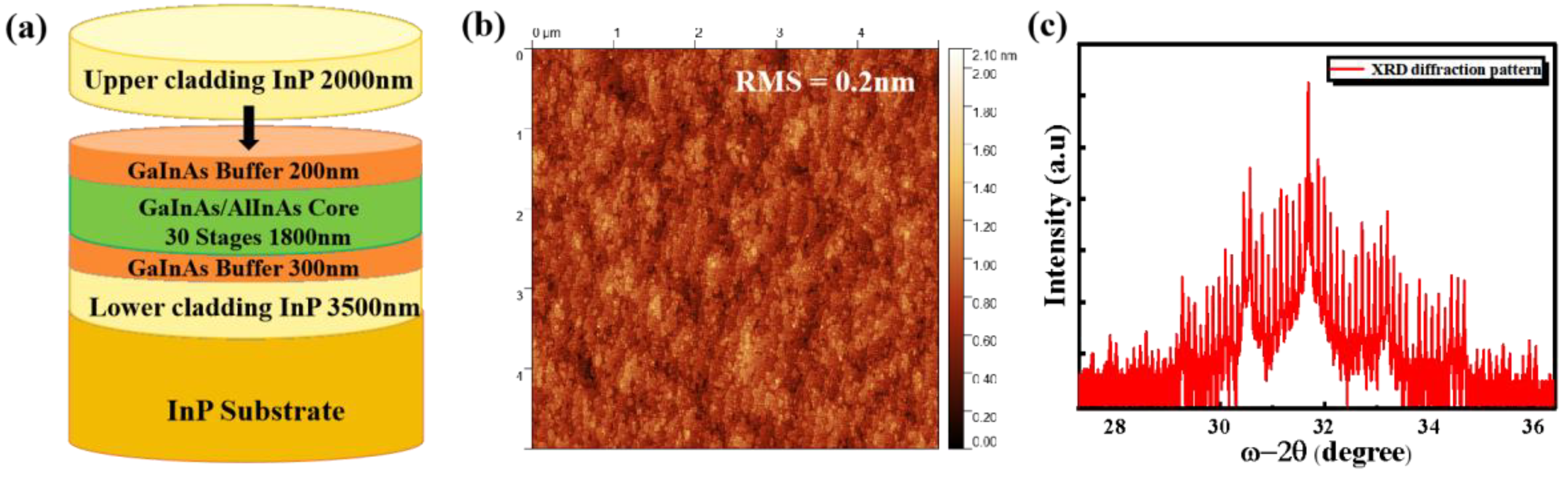
Figure 2.
Effects of different contents of three liquids on corrosion rate and roughness.
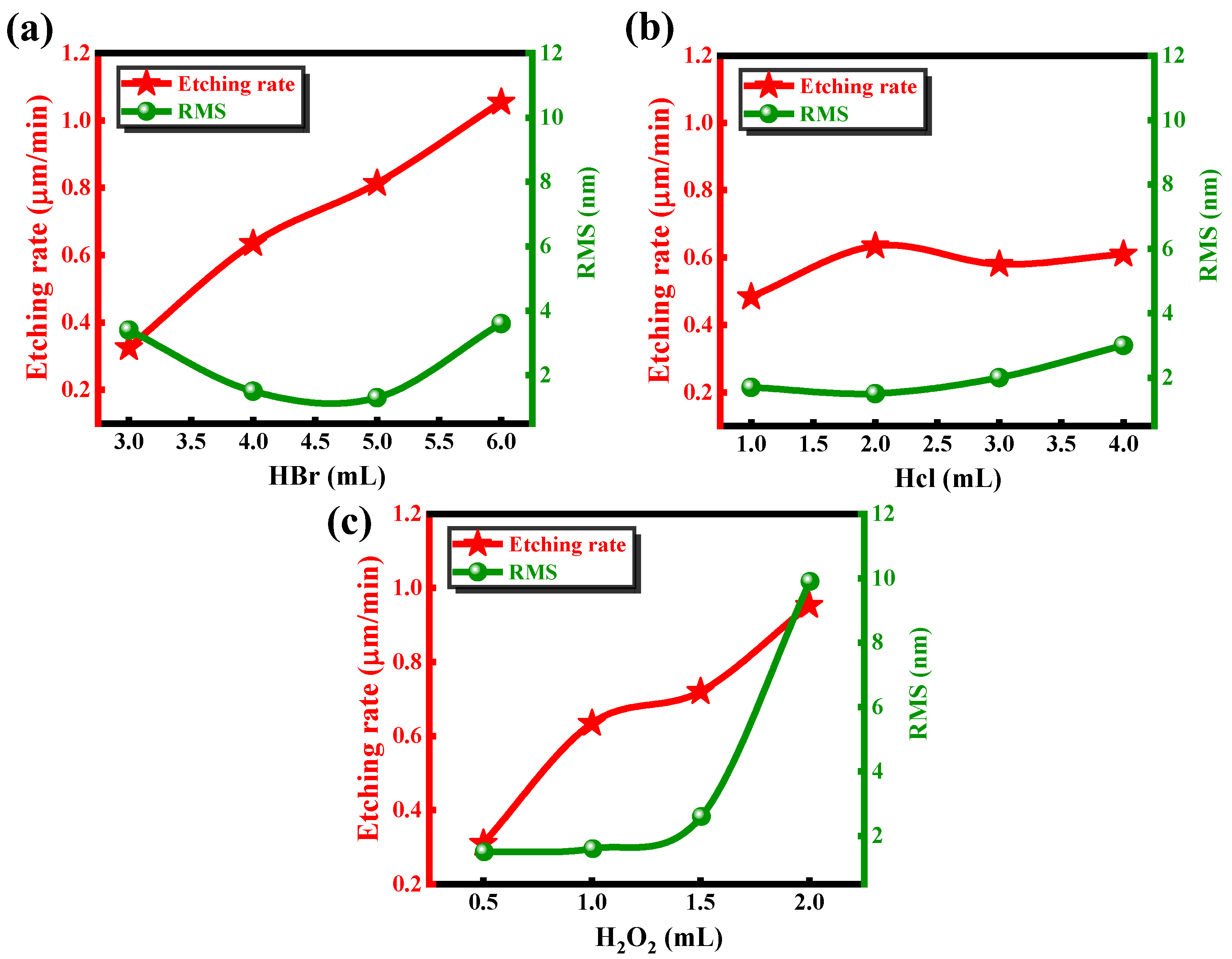
Figure 3.
5 µm × 5 µm AFM images. (a) Untreated sample (b) Sample after etching with BHD solution (c) Sample after etching with CHD solution (d) Sample after etching with BCD solution (e) Sample after etching with BCHD solution.
Figure 3.
5 µm × 5 µm AFM images. (a) Untreated sample (b) Sample after etching with BHD solution (c) Sample after etching with CHD solution (d) Sample after etching with BCD solution (e) Sample after etching with BCHD solution.
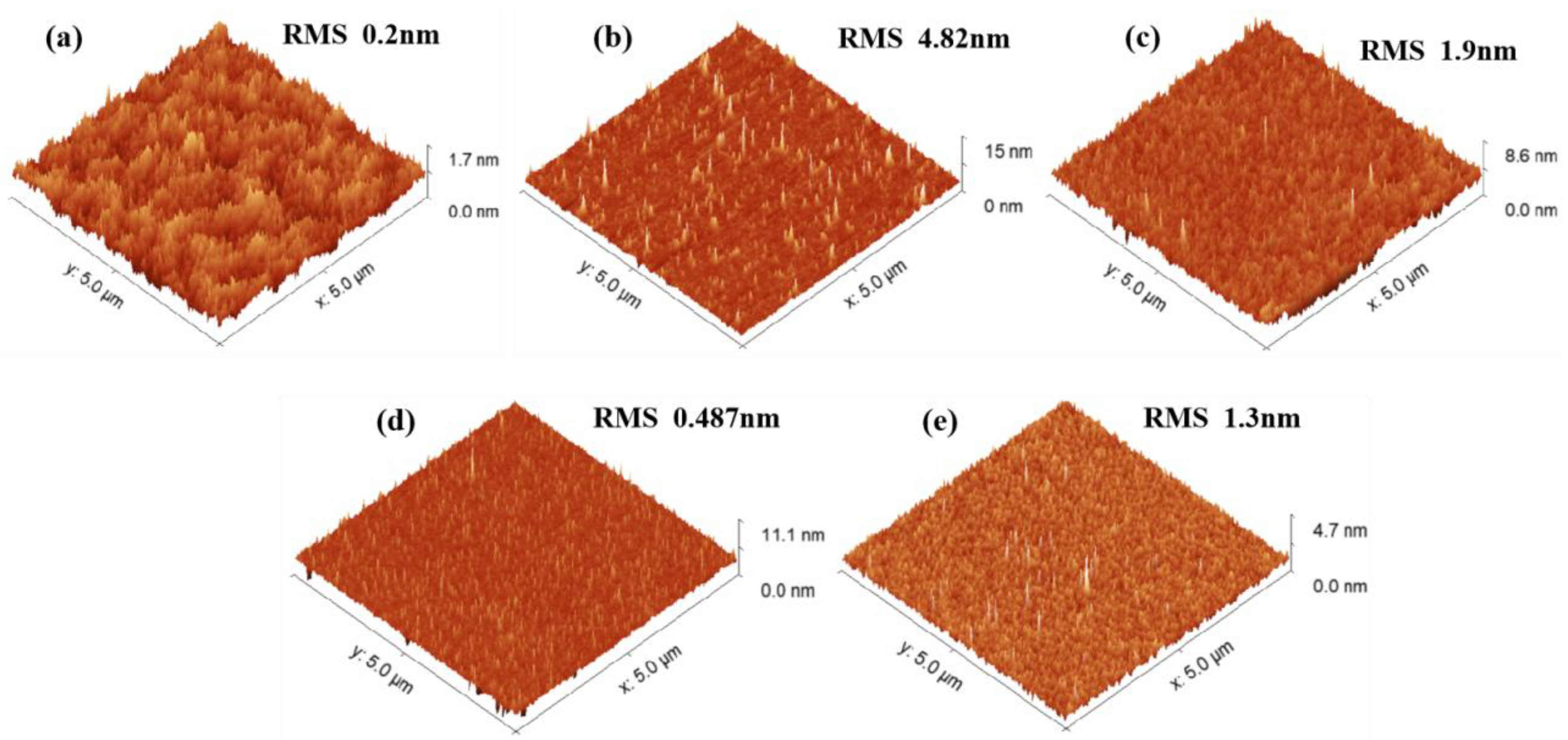
Figure 4.
XPS spectra of samples were etched for 2 minutes with BCHD, BHD, CHD, and BCD solutions. (a) InP (100) surface showing In 4d and P 2p peaks. (b) GaInAs/AlInAs superlattice showing As 3d, Ga 3d & In 4d, and Al 2p peaks.
Figure 4.
XPS spectra of samples were etched for 2 minutes with BCHD, BHD, CHD, and BCD solutions. (a) InP (100) surface showing In 4d and P 2p peaks. (b) GaInAs/AlInAs superlattice showing As 3d, Ga 3d & In 4d, and Al 2p peaks.
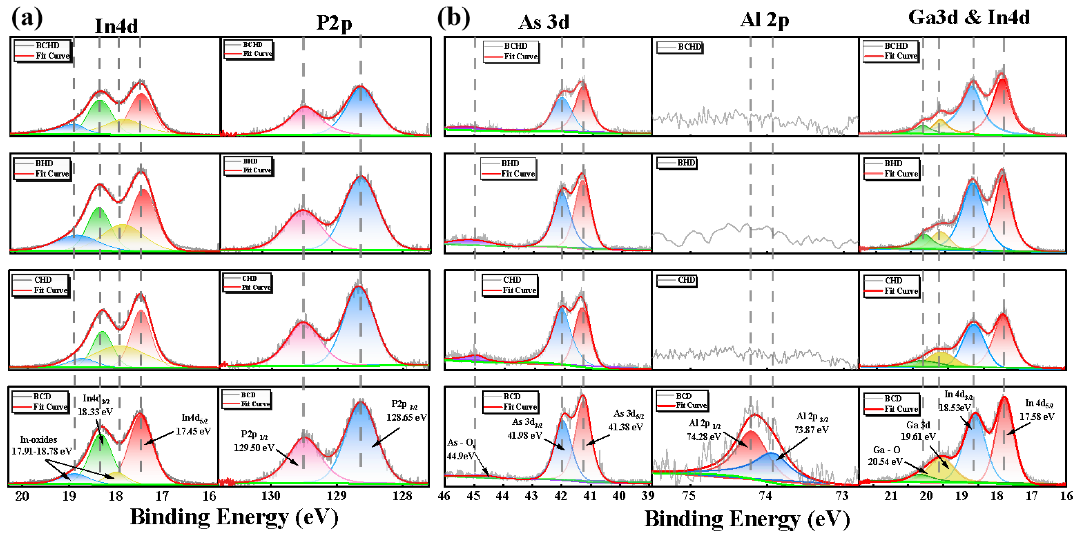
Figure 5.
Ridge Profile after BCHD Etching (a) Perpendicular to the wafer major flat (b) Parallel to the wafer major flat (c) Tilted at a 45-degree angle to the major flat.
Figure 5.
Ridge Profile after BCHD Etching (a) Perpendicular to the wafer major flat (b) Parallel to the wafer major flat (c) Tilted at a 45-degree angle to the major flat.
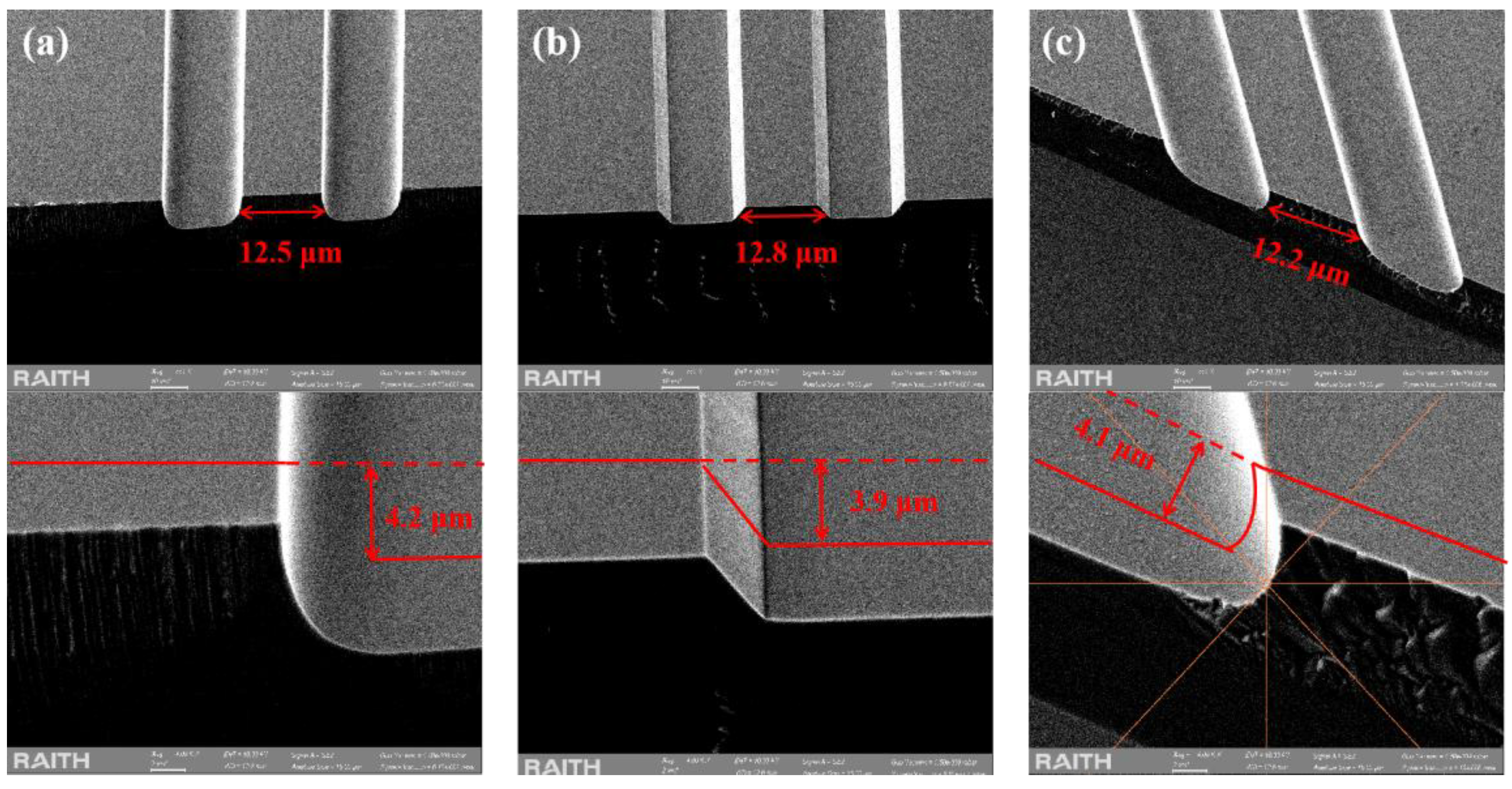
Table 2.
XPS Spectrum Analysis of Elemental Composition on the Sample Surface.
| Peak | Component | Intensity Ratio Versus Bulk | |||
|---|---|---|---|---|---|
| BCHD | BHD | CHD | BCD | ||
| P 2p | P 2p 3/2 | 60.42% | 62.47% | 62.61% | 61.4% |
| P 2p 1/2 | 39.58% | 37.53% | 37.39% | 38.6% | |
| In 4d | In-P | 73.34% | 70.13% | 68.38% | 79.63% |
| In-O | 26.66% | 29.87% | 31.62% | 20.38% | |
| As 3d | As | 92.4% | 84.17% | 90.34% | 96.15% |
| As-O | 7.6% | 15.83% | 9.66% | 3.85% | |
| Al 2p | Al-As | / | / | / | 42.3% |
| Al-O | / | / | / | 57.7% | |
| Ga3d & In4d | Ga-As | 8.43% | 8.21% | 14.2% | 15.5% |
| Ga-O | 6.28% | 9.17% | 6.73% | 4.05% | |
| In 4d5/2 | 40.29% | 39.6% | 42.13% | 41.4% | |
| In 4d3/2 | 45% | 43.01% | 36.94% | 39.05% | |
Disclaimer/Publisher’s Note: The statements, opinions and data contained in all publications are solely those of the individual author(s) and contributor(s) and not of MDPI and/or the editor(s). MDPI and/or the editor(s) disclaim responsibility for any injury to people or property resulting from any ideas, methods, instructions or products referred to in the content. |
© 2025 by the authors. Licensee MDPI, Basel, Switzerland. This article is an open access article distributed under the terms and conditions of the Creative Commons Attribution (CC BY) license (http://creativecommons.org/licenses/by/4.0/).
Copyright: This open access article is published under a Creative Commons CC BY 4.0 license, which permit the free download, distribution, and reuse, provided that the author and preprint are cited in any reuse.


