
Submitted:
31 October 2025
Posted:
04 November 2025
You are already at the latest version
Abstract
The article compares the properties of coatings deposited on a stainless steel substrate with surface preparation using the Hollow Cathode Spaces (HCS) and Ion Bombardment (IB) methods. After coating deposition, the wear resistance of the samples increases by 40–50 % compared to uncoated samples, while the use of the HCS method ensures wear resistance that is 15 % higher than the IB method. Samples with coatings deposited using the HCS and IB methods demonstrate very similar friction coefficient values, with an insignificant (10 %) decrease in this indicator for the HCS samples. The best wear resistance is observed for the HCS sample, the surface of which was prepared at a bias voltage of –1200 V. This bias voltage value ensures the best parameters for the coated sample compared to samples whose surface preparation was carried out at a higher (–1500 V) or lower (–900 V) bias voltage. A substrate bias voltage of –1200 V provides not only improved wear resistance in the pin-on-disc test but also improved resistance to damage in the scratch test. Analysis of the interface between the coating and the stainless steel substrate revealed that the HCS method produces a transition layer 15–25 nm thick. This transition layer includes zirconium, nickel, and iron, with a small amount of chromium. The IB method also produces a similar transition layer in the interface area, but with a thicker thickness of 100–150 nm.
Keywords:
hollow cathode spaces
; ion bombardment
; stainless steel
; wear
; friction
; pin-on-disc test
1. Introduction
AISI 321 stainless steel is widely used in many industries [1,2,3,4]. Products made from this steel can withstand high temperatures for long periods without losing their properties. These properties are due to the alloy’s 0.5% titanium content. This composition results in a strong, hermetic weld that is resistant to corrosion.
- high corrosion resistance, due in part to the presence of chromium;
- high heat and thermal shock resistance, allowing it to be used at temperatures up to +600 °C. At this temperature, the steel’s structure remains unchanged for a considerable period;
- good weldability, ensured by its low carbon content;
- good ductility, which improves the machinability of products made from this steel.
In addition, this steel is classified as hygienic and is widely used in the food and medical industries. Although AISI 321 steel has a number of useful properties and is widely used in various industries, increasingly stringent requirements for modern materials necessitate the search for ways to further improve its performance. In particular, increased wear resistance of AISI 321 steel products is required. To further enhance the wear resistance of AISI 321 steel products, special modifying coatings of various compositions and deposition methods are effectively used [1,6,7,8,9,10]. Coatings deposited on an AISI 321 steel substrate using Physical Vapor Deposition (PVD) have demonstrated high effectiveness in terms of corrosion resistance and wear resistance [9,10].
The performance of coatings in general, and PVD coatings in particular, is associated not only with their mechanical and chemical properties, but to a significant extent with the strength of adhesion between the coating and the substrate. In turn, adhesion is ensured by effective preparation of the substrate surface – cleaning from microcontamination and thermal activation [11,12,13,14,15,16,17,18]. Cleaning and heating (thermal activation) of the substrate surface can be accomplished using infrared heating or laser beam exposure [12,14,19,20,21,22]. These methods have certain advantages, but require additional equipment and complicate the technological process. Preliminary treatment of the substrate surface with an accelerated ion stream is used in most cases due to its relative simplicity and the use of equipment already available in the vacuum plasma unit [13,14,16,18,22,23,24,25,26,27,28]. This method is implemented by bombarding the substrate surface with ions (metals, gases, or a mixture of these [28,29]), whereby the energy of the accelerated ions is transferred to the substrate atoms, producing a dual effect. On the one hand, weakly bound atoms (primarily contaminants) are knocked out from the substrate surface (cleaning), and on the other hand, the surface layers of the substrate are heated (thermal activation) [11,30,31,32]. At high energy, the impacting ions can be embedded in the outer layers of the substrate, making it possible, for example, to achieve surface nitriding or implant atoms of the sputtered metal into the substrate [20,32,33,34,35]. Another effect of ion bombardment can be a decrease in the roughness of the substrate surface and a reduction in its defects [15,19,20,21]. The ion bombardment process is influenced by a number of factors, including the ion energy and ion flux density (depending on the substrate bias voltage, cathode arc current, substrate and cathode materials, and working gas composition), the angle of ion incidence relative to the substrate surface (depending on the substrate and tooling geometry, substrate movement kinetics, and its surface microgeometry), and treatment duration [20,31,36,37,38,39,40]. Substrate bias voltage is one of the key process control parameters and typically ranges from 200 to 1500 V [32,41]. Despite its relative simplicity and high efficiency, the ion bombardment method also has some significant disadvantages. These include uneven distribution of ion current density across the plasma flow cross-section, which results in uneven heating of the workpieces [15,39,42]. The power of the ion flux also determines the possibility of re-deposition of contaminants (including the material of the equipment and chamber walls) onto the substrate [43,44,45,46]. Furthermore, this method requires a fairly long period of operation of the cathode systems, which is associated with high energy consumption.
Another method for efficient substrate surface preparation is ion cleaning in a self-sustaining stationary glow discharge plasma [11,13,27,43,44,45]. This method is based on the acceleration of gas plasma ions onto the substrate surface, with the substrate itself acting as the glow discharge cathode or as an additional negative electrode relative to the plasma. This treatment allows for efficient cleaning and thermal activation of the substrate surface, ensuring good coating adhesion [47,48,49,50]. At the same time, irregular distribution of the electric field strength over the surface of the substrate being treated can lead to uneven heating [51,52]. This problem is solved using various glow discharge schemes, among which the use of a “hollow” cathode is very effective. This implies the presence of a closed or quasi-closed equipotential cavity in such a cathode, within which the discharge is localized due to the fact that the emitted electrons oscillate, repeatedly reflecting from its walls. During the process of such oscillation, a significant increase in the degree of gas ionization and the density of the glow discharge plasma occurs [53].
In this study, we used a method for heating and cleaning the surface of workpieces using a glow discharge, using Hollow Cathode Spaces (HCS) [54]. The hollow cathode effect was achieved through the specific arrangement of the workpieces, which are positioned in a vacuum chamber on a rotary table. Their surfaces form a partially enclosed internal region—the quasi-cavity of the hollow cathode.
To eliminate the influence of additional factors on the results of the study, a coating of a simple two-component composition (ZrN) was deposited.
2. Materials and Methods
The studied coatings were deposited on a VIT-2 PVD system (IDTI RAS – MSUT «STANKIN», Moscow, Russia) [55,56,57,58,59,60]. A distinctive feature of this system is the use of filtered cathodic vacuum arc deposition (FCVAD) systems [61,62], which ensure efficient separation of the microdroplet phase in combination with a Controlled Accelerated Arc (CAA-PVD) system [29,63,64,65], which ensures high energy efficiency.
A planetary rotation fixture is located within the vacuum chamber, comprising 12 racks (rods) with sample mounting devices. A negative voltage ranging from 0 to -1500 V is applied to the fixture, with a permissible current of 30 A. The vacuum chamber walls serve as the anode. A Zr cathode (99.8%) was used.
The gas (nitrogen) pressure ranged from 130 to 1300 Pa, and the sample surface temperature was monitored using an Ircon Modline Plus Infrared Thermometer (Fluke Process Instruments, Everett, WA, USA) and remained in the range of 500–600 °C.
Two alternative processes for surface preparation of products before coating deposition were compared: Hollow Cathode Spaces (HCS) and Ion Bombardment (IB).
Hollow cathode spaces (HCS) Cleaning and heating are performed in a glow discharge plasma at a pressure of 5.0 Pa. Parts in a vacuum chamber form hollow cathode spaces. Argon (Ar) uses as the working gas. Initially, for the HCS cleaning and heating processes, a minimum voltage is applied to the turntable, at which the glow discharge begins (approximately -100 V). As the microarcs disappear, the voltage increases until the sample temperature reaches 650 °C. Ion cleaning and heating occur by bombarding the surface (glow discharge cathode) with positively charged gas ions accelerated in the cathode layer of the discharge. A detailed description of the processes of cleaning and thermal activation of the surface using the HCS method is contained in [54].
Ion bombardment (IB) Arc evaporators are switched on to generate metal plasma, and the arc-burning current on all evaporators is 90 A. The pressure in the working chamber is not higher than 0.005 Pa. A negative voltage of -100 V from a high-voltage power source is applied to the rotary table with the parts fixed on it. As the heating proceeds and the probability of microarcs decreases, the voltage gradually increases until the surface temperature of the parts reaches 650 °C.
The structure of the deposited coatings included a thin adhesion layer of metallic zirconium (30–50 nm thick) and a wear-resistant ZrN layer approximately 3 μm thick.
To study the effect of HCS process parameters (bias voltage) on the wear resistance of the coated samples, three deposition processes were conducted. Table 1 shows the sample designations depending on the substrate bias voltage used in the HCS process. The remaining parameters were held constant for all three deposition processes. Samples with different HCS process parameters, as well as a sample prepared using the IB method, were compared.
Scratch testing was performed using a Nanovea scratch tester (Nanovea, Irvine, CA, USA) in accordance with ASTM C 1624 [66] over a load range of 0–40 N using a conical diamond indenter with an angle of 120° and a radius of 100 μm. Three measurements were taken for each type of coating, after which the average value and the range of values were deter-mined.
An automated mechanical tester, the SV-500 (Nanovea, Irvine, CA, USA), was used to study the hardness. The measurement method was performed using instrumental indentation with a Berkovich pyramidal indenter. The measurement modes were at the maximum load at 20 mN.
A DUCOM POD-4.0 (Ducom Instruments Pvt. Ltd., Bangalore, India) universal tribometer was used to conduct friction and wear tests using a pin-on-disk/ball-on-disk system. The loading scheme used in this device ensured that the working fluid (ball) load was set independently of the friction console, which reduced vibrations in the system and increased the accuracy of the tests. The load was 10 N, and the rotation speed was 100 rpm. Furrow radius 10–12 mm. The tests were conducted over 30,000 s (about 8½ h), using an indenter (ball) made of ASTM 52100 bearing steel, the properties of which are similar to those of the sample mate-rial. The wear resistance was determined according to ASTM G99 [67]. The testing was conducted at room temperature and without any lubricant. The wear results are presented as the volume loss in cubic millimeters for the test sample (coated disk) and as the mass loss for the ball. Three measurements were taken for each type of coating, after which the average value and the range of values were determined.
3. Results
3.1. Comparison of the Effectiveness of Using HCS and IB Methods
The hardness of all deposited coatings, measured using a nanoindentometer, was 27.3 ± 1.2 GPa. No significant difference in hardness was observed between coatings deposited using the HCS and IB methods.
The results of the pin-on-disk wear resistance study for substrates of various compositions with coatings deposited using the IB and HCS methods, as well as without coating, are shown in Figure 1a. After coating deposition, the wear resistance of the samples increased by 40–50% compared to uncoated samples, with the HCS method providing 15 % higher wear resistance than the IB method.
Coatings deposited on a steel substrate significantly affect the tribological properties of the samples, reducing the friction coefficient from 0.5 to 0.2, i.e., by a factor of 2.5 (Figure 1b). From a tribological standpoint, samples with coatings deposited using the HCS and IB methods demonstrate very similar friction coefficient values, with an insignificant (10%) decrease in this indicator for the HCS samples. This result is due to the fact that the use of the HCS or IB methods primarily affects the interface area of the coating and the substrate and, accordingly, the adhesion strength between them. The influence of the substrate surface preparation method on the properties of the coating surface layer is not as significant, but there is a relationship between the condition of the substrate surface and the structure (in particular, the grain size) of the deposited coating [68,69,70,71]. For example, it was found that (Cr,Al)N coatings vary in their texture and mechanical properties, particularly hardness and residual stresses, depending on the surface condition of the 316L steel substrate. The substrate surface condition influences the direction of coating texture growth, which in turn influences the magnitude of residual stresses that promote spinodal decomposition of the metastable cubic phase of the coating [68].
3.2. Determining the Optimal Value of Substrate Bias Voltage Using the HCS Method
Such a key parameter of the HCS process as bias voltage has a significant impact on the quality of substrate surface preparation and, accordingly, the quality of the coating as a whole [72,73,74,75]. The results of the study of the effect of bias voltage on wear resistance in the pin-on-disc test are presented in Figure 2. At a bias voltage of –900 V, the wear resistance of the HCS samples is lower than that of the IB sample, and at a bias voltage of –1500 V, the wear resistance of the HCS sample is almost identical to that of the IB sample. The best wear resistance is observed for the HCS 2 sample, the surface of which was prepared at a bias voltage of –1200 V. Thus, the initially determined bias voltage of –1200 V ensures the best parameters of the coated sample compared to the samples whose surface preparation was carried out at a higher (–1500 V) or lower (–900 V) bias voltage.
Since the studies were conducted at only three bias voltage values, it is possible that the optimal bias voltage value differs from –1200 V and may be biased upward or downward.
To find the optimal bias voltage value, we will construct an approximating curve for the wear rate versus bias voltage (Figure 3). As is known, an approximating curve (empirical formula) is an approximate functional relationship obtained based on experimental data [76,77]. Thus, the approximation task consists of constructing a function that most accurately reflects the overall trend. To assess the adequacy of the approximating curve to the available experimental data, the approximation reliability value (determination coefficient) R2 is used, which determines the proportion of the variance of the dependent variable determined by the independent variables. In this case, the second-degree polynomial (quadratic function) most accurately (with the best value of R2 = 1) describes the general relationship between wear and bias stress. The corresponding relationships are presented on the graph and as a formula (see Figure 3).
Having obtained the approximating function, we determine the optimal value of the bias voltage. To do this, we determine the extremum of the function. In our case, this is the point in the function’s domain where the function value is minimal (the wear is minimal). Finding the extremum of a function involves finding the derivative of the function, determining the point at which the derivative is zero (or nonexistent if the function has a discontinuity), and checking whether the derivative changes sign at this point. A change in the derivative’s sign indicates the presence of a minimum.
Let’s determine the optimal value of the bias voltage.
The approximating dependence is determined by the quadratic formula
where x is the substrate bias voltage, V; y is the wear value after completion of the experiment (10−6 mm3/N · m).
y = 0.0005 · x2 + 1.2122 · x + 906.13,
We find the first derivative of the function:
y′ = 0.001 · x + 1.2122.
We equate it to zero:
0.001 · x + 1.2122 = 0, thereby x1 = –1212.2.
We calculate the values of the function
f(–1212.2) = 171.416.
Let’s check. We’ll use the sufficient condition for an extremum of a function of one variable. We’ll find the second derivative:
y″ = 0.001.
We calculate:
f″(–1212.2) = 0.001 > 0.
Thus, the minimum value of the function corresponding to the optimal substrate bias voltage, ensuring minimal wear, was obtained. This value is –1212.2 V, which is practically identical to the value of –1200.0 V used in the experiments.
3.3. Research of Wear Patterns of Samples and Structure of the Interface Between the Coating and the Substrate
The wear patterns of the samples after the pin-on-disc test show obvious differences (Figure 4). Only the HCS 2 coating is fragmentarily preserved in the central portion of the wear striation. Along the edges of the wear striation, this sample exhibits smooth coating wear without the formation of distinct boundaries. On the remaining samples, the coating in the wear striation area is completely lost, and the striation itself has clearly defined boundaries. The widest wear striation (and, consequently, the greatest volume of material removed, as confirmed by the previously presented data) is observed on sample IB, which correlates with the previously obtained data (see Figure 1).
Figure 5 and Figure 6 show a more detailed view of the surface wear striations during the pin-on-disk test on a stainless steel specimen with HCS 2 and IB coatings, respectively. The failure of the HCS 2 coating is characterized by fragmentary breakouts, but no clearly defined striation edge is formed; significant areas of intact coating remain within the striation (Figure 5). Conversely, the wear of the IB coating (Figure 6) is characterized by the formation of clearly defined striation edges; within the striation itself, the coating is completely lost.
An analysis of the interface between the coating and the stainless steel substrate using the HCS method (Figure 7) shows that there are no noticeable discontinuities or adhesion issues in this area. A transition layer 15–25 nm thick is observed between the coating and the substrate (Figure 7b–7d). This layer is formed by a mixture of iron (approximately 43 at.%), zirconium (approximately 38 at.%), chromium (approximately 18 at.%), and nickel (approximately 1–2 at.%). It is worth noting the significant decrease in the nickel content in this layer compared to the substrate (approximately 20 at.%). Structurally, this layer is characterized by a nanoscale granular structure with grain sizes of 10–30 nm.
Further studies of the elemental composition in the interface area reveal weak interdiffusion of coating elements (zirconium) and the substrate (iron, nickel, chromium) (Figure 8). This adhesion is no longer observed at a distance of 30 nm from the interface layer.
When using the IB method, the interface has some differences. A layer with a thickness of 100–150 nm is formed in the interface region (Figure 9a). In this layer, an increased nickel content (up to 20–28 at.%) and a decreased chromium content (from 15–18 to 2–4 at.%) are observed (Figure 9). At the same time, directly in the surface layer of the substrate, at a depth of about 150 nm, a decrease in the nickel content is observed from 11–12 at.% to values close to 0. Thus, in terms of elemental composition, the studied transition layer includes zirconium (60–63 at.%), nickel (20–28 at.%), iron (6–18 at.%) with an insignificant chromium content (2–4 at.%). Interdiffusion of the coating and substrate elements is minimal, as in the case of the HCS coating. Only in one case is a slight diffusion of iron into the coating observed (Figure 9c).
It is possible to assume the formation of nickel-zirconium in the layer under consideration, which is a binary inorganic compound of nickel and zirconium with the formula ZrNi, Ni5Zr, or Zr2Ni. Nickel-zirconium is known to form during the sintering of stoichiometric quantities of pure substances (nickel and zirconium) [78,79,80]. At concentrations above 1 wt.% zirconium in the alloys, corrosion resistance decreases, ductility, and machinability deteriorate. This occurs due to the precipitation of a significant amount of the second phase (the metallic compound Ni5Zr) along the grain boundaries of the solid solution.
3.4. Resistance of Samples with the Studied Coatings to Destruction During Scratch Testing
The scratch test is a generally accepted method for determining coating-to-substrate adhesion. Research has shown that the best scratch test failure resistance was achieved with the HCS-2 surface preparation method (Figure 10). While the initial failure force (LC1) was fairly similar for all samples (around 4 N), with a slight advantage for the HCS-2 sample (4.5 N), the HCS-2 sample demonstrated a significant advantage in the total coating failure load (LC2) 8–9 N (compared to 6–7 N for the other samples). Thus, the HCS-2 surface preparation conditions not only ensured better wear resistance in the pin-on-disc test but also better scratch test failure resistance.
Although the coating on the stainless steel substrate is destroyed under relatively high loads (LC2 = 6–9 N), no large areas of coating peeling off from the substrate are observed, i.e., the destruction occurs mainly due to processes in the coating itself, and not due to peeling of the coating from the substrate (Figure 11).
4. Conclusions
• After coating deposition, the wear resistance of the samples increases by 40–50% compared to uncoated samples, with the HCS method providing 15% higher wear resistance than the IB method.
• Coated samples deposited using the HCS and IB methods demonstrate very similar friction coefficient values, with a slight (10%) decrease in this indicator for the HCS samples.
• The best wear resistance is observed for the HCS 2 sample, the surface of which was prepared at a bias voltage of –1200 V. Thus, the initially determined bias voltage of –1200 V ensures the best parameters for the coated sample compared to samples whose surface preparation was carried out at a higher (–1500 V) or lower (–900 V) bias voltage.
• The minimum value of the function corresponding to the optimal substrate bias voltage, ensuring minimal wear, was calculated. This value is –1212.2 V, which is practically identical to the –1200.0 V value used in the experiments. Accordingly, a bias voltage of –1200 V can be recommended for preparing the surface of a stainless steel substrate using the HCS method.
• Analysis of the nature of the interface between the coating and the stainless steel substrate using the HCS method revealed that a transition layer 15–25 nm thick is formed. This layer is formed by a mixture of iron (approximately 43 at.%), zirconium (approximately 38 at.%), chromium (approximately 18 at.%), and nickel (approximately 1–2 at.%).
• When using the IB method, a layer 100–150 nm thick is formed in the interface area, which includes zirconium (60–63 at.%), nickel (20–28 at.%), iron (6–18 at.%) with an insignificant content of chromium (2–4 at.%).
• The HCS-2 sample demonstrated a significant advantage in terms of the coating failure load (LC2) 8–9 N (compared to 6–7 N for the other samples).
Thus, the HCS-2 surface preparation conditions provide not only better wear resistance in the pin-on-disc test but also better resistance to damage in the scratch test.
Author Contributions
Conceptualization, Y.B., A.V.; Methodology, Y.B., C.S., F.M. and A.S.; Resources, A.V.; Data curation, C.S., T.B. and Y.P.; investigation, C.S., F.M., A.S., I.S., E.E., T.B., and Y.P.; Supervision, Y.B. and A.V.; Writing—original draft preparation, A.V.; Writing—review and editing, A.V., T.B. and C.S.; Project administration, A.V. and C.S. All authors have read and agreed to the published version of the manuscript.
Funding
This work was funded by the Russian Science Foundation (grant No. 24-19-00413).
Institutional Review Board Statement
Not applicable.
Informed Consent Statement
Not applicable.
Data Availability Statement
The original contributions presented in the study are included in the article; further inquiries can be directed to the corresponding author.
Conflicts of Interest
The authors declare no conflicts of interest.
References
- Huang, Z.; Zhang, J.; Ma, Z.; Yuan, S.; Yang, H. Research Progress on the Relationship Between Microstructure and Properties of AISI 321 Stainless Steel. Appl. Sci. 2024, 14, 10196. [CrossRef]
- Kasana, S.S.; Pandey, O. Effect of heat treatment on microstructure and mechanical properties of boron containing Ti-Stabilized AISI-321 steel for nuclear power plant application. Mater. Today Commun. 2021, 26. [CrossRef]
- Zhang, W.; Wu, J.; Wen, Y.; Ye, J.; Li, N. Characterization of different work hardening behavior in AISI 321 stainless steel and Hadfield steel. J. Mater. Sci. 2010, 45, 3433–3437. [CrossRef]
- Chen, H.; Li, W.; Chen, W.; Chen, J.; Zhang, S. Influence of prior creep-fatigue exposure on remnant tensile and creep properties of AISI 321 austenite stainless steel. Int. J. Fatigue 2022, 159. [CrossRef]
- Tiamiyu, A.A.; Eduok, U.; Szpunar, J.A.; Odeshi, A.G. Corrosion behavior of metastable AISI 321 austenitic stainless steel: Investigating the effect of grain size and prior plastic deformation on its degradation pattern in saline media. Sci. Rep. 2019, 9, 12116. [CrossRef]
- Wiaderek, K.J. The structure, properties and change in the cross-sectional corrosion resistance of a nitrided layer produced on AISI 321 steel. Int. J. Surf. Sci. Eng. 2016, 10, 503–513. [CrossRef]
- Muthu, S.M.; Arivarasu, M.; Krishna, T.H.; Ganguly, S.; Prabhakar, K.V.P.; Mohanty, S. Improvement in hot corrosion resistance of dissimilar alloy 825 and AISI 321 CO2-laser weldment by HVOF coating in aggressive salt environment at 900°C. Int. J. Miner. Met. Mater. 2020, 27, 1536–1550. [CrossRef]
- Simon, C.R.; Haugsrud, R.; Musiani, M.; Barison, S.; Walmsley, J.C.; Jacques, T.; Bredesen, R. Effects of Silica Nano-Particle Coatings on High-Temperature Oxidation of AISI 321. Mater. Sci. Forum 2004, 461-464, 281–288. [CrossRef]
- Bauyrzhan, R.; Alexander, P.; Zhuldyz, S.; Dastan, B.; Vyacheslav, B.; Mukhamedova, A. Effect of Bilayer Thickness and Bias Potential on the Structure and Properties of (TiZr/Nb)N Multilayer Coatings as a Result of Arc-PVD Deposition. Materials 2022, 15, 7696. [CrossRef]
- Grigoriev, S.; Volosova, M.; Sotova, C.; Milovich, F.; Seleznev, A.; Makarevich, K.; Potapov, P.; Vereschaka, A. Increasing the Wear Resistance of Stainless Steel Products by Depositing Modifying Coatings Based on Zirconium Nitride with the Addition of Niobium, Hafnium, and Titanium. J. Manuf. Mater. Process. 2025, 9, 316. [CrossRef]
- Frey, H.; Khan, H.R. Handbook of Thin Film Technology. Springer-Verlag Berlin Heidelberg, 2015.
- Grigorovich, K.V.; Petrov, L.M.; Sprygin, G.S.; Smirnova, A.N. Features of the Formation of Surface Layers on Metal Materials by the of Electric Arc Vacuum-Ion-Plasma Deposition Method. Russ. Met. (Metally) 2022, 2022, 1449–1455. [CrossRef]
- Luchkin, A.G.; Luchkin, G.S. Cleaning the Surface of Substrates for Coating by Vacuum-Plasma Methods. Bulletin of the Kazan Technological University 2012, 15, 208–210.
- Oura, K.; Lifshitz, V.G.; Saranin, A.A.; Zotov, A.V.; Katayama, M. Introduction to surface physics. Nauka, Moscow, 2006.
- Tillmann, W.; Hagen, L.; Stangier, D.; Krabiell, M.; Schröder, P.; Tiller, J.; Krumm, C.; Sternemann, C.; Paulus, M.; Elbers, M. Influence of etching-pretreatment on nano-grained WC-Co surfaces and properties of PVD/HVOF duplex coatings. Surf. Coatings Technol. 2019, 374, 32–43. [CrossRef]
- Pemmasani, S.P.; Valleti, K.; Gundakaram, R.C.; Rajulapati, K.V.; Mantripragada, R.; Koppoju, S.; Joshi, S.V. Effect of microstructure and phase constitution on mechanical properties of Ti1−xAlxN coatings. Appl. Surf. Sci. 2014, 313, 936–946. [CrossRef]
- Yang, J.; Odén, M.; Johansson-Jõesaar, M.; Esteve, J.; Llanes, L. Mechanical strength of ground WC-Co cemented carbides after coating deposition. Mater. Sci. Eng. A 2017, 689, 72–77. [CrossRef]
- Barshilia, H.C.; Ananth, A.; Khan, J.; Srinivas, G. Ar + H2 plasma etching for improved adhesion of PVD coatings on steel substrates. Vacuum 2012, 86, 1165–1173. [CrossRef]
- Buchwalder, A.; Zenker, R. Pre- and post-surface treatments using electron beam technology for load-related application of thermochemical and PVD hard coatings on soft substrate materials. Surf. Coatings Technol. 2019, 375, 920–932. [CrossRef]
- Guo, X.; Liu, F.; Zhang, K.; Wang, C.; Piao, Z.; Sun, L. Controllable preparation of micro-textures on WC/Co substrate surface by an integrated laser-dry etching process for improving PVD coatings adhesion. Appl. Surf. Sci. 2020, 534. [CrossRef]
- Zhang, K.; Deng, J.; Guo, X.; Sun, L.; Lei, S. Study on the adhesion and tribological behavior of PVD TiAlN coatings with a multi-scale textured substrate surface. Int. J. Refract. Met. Hard Mater. 2018, 72, 292–305. [CrossRef]
- Meng, X.; Zhang, K.; Guo, X.; Wang, C.; Sun, L. Preparation of micro-textures on cemented carbide substrate surface by plasma-assisted laser machining to enhance the PVD tool coatings adhesion. J. Mech. Work. Technol. 2021, 288. [CrossRef]
- Stepanovsky, A.S. Ionic Processing of Materials. Mechanical Engineering: Science and Technology 2013, 14.
- Komarovskaya, V.M.; Ivashchenko, S.A. Optimization of modes of ion treatment of the surface of non-metallic materials. Hardening Technologies And Coatings 2013, 3, 23–27.
- Zabrodin, I.G.; Zorina, M.V.; Kaskov, I.A.; Malyshev, I.V.; Mikhailenko, M.S.; Pestov, A.E.; Salashchenko, N.N.; Chernyshev, A.K.; Chkhalo, N.I. Ion-beam techniques for precision processing of optical surfaces. J. Tech. Phys. 2020, 90(11), 1922–1930.
- Grebenyuk, V.F.; Rudakov, V.I. Ion-plasma technology for hardening a deforming tool. Vestnik OGU 2003, 5, 137–140.
- Berlin, E.; Dvinin, S.; Seidman, L., World of Materials and Technologies. Vacuum technology and equipment for deposition and etching of thin films. Technosphere, Moscow, 2007.
- Hovsepian, P.; Reinhard, C.; Ehiasarian, A. CrAlYN/CrN superlattice coatings deposited by the combined high power impulse magnetron sputtering/unbalanced magnetron sputtering technique. Surf. Coatings Technol. 2006, 201, 4105–4110. [CrossRef]
- Grigoriev, S.; Vereschaka, A.; Zelenkov, V.; Sitnikov, N.; Bublikov, J.; Milovich, F.; Andreev, N.; Sotova, C. Investigation of the influence of the features of the deposition process on the structural features of microparticles in PVD coatings. Vacuum 2022, 202. [CrossRef]
- Berish, R. Problems of Applied Physics. Sputtering of solids by ion bombardment 1986, II, 482.
- Lieberman, M.A.; Lichtenberg, A.J. Principles of Plasma Discharges and Materials Processing, 2nd ed.; Wiley: Hoboken, NJ, USA, 2005.
- Lattemann, M.; Ehiasarian, A.; Bohlmark, J.; Persson, P.; Helmersson, U. Investigation of high power impulse magnetron sputtering pretreated interfaces for adhesion enhancement of hard coatings on steel. Surf. Coatings Technol. 2006, 200, 6495–6499. [CrossRef]
- Mukha, I.M.; Shcherbakova, L.I. Effect of Heating by a Glow Discharge on the Surface State of Transition-Metal Carbides. Elektronnaya Obrabotka Materialov 1976, 3, 53–56.
- Mattox, M.D. A Short History of In Situ Cleaning in Vacuum for Physical Vapor Deposition (PVD). SVC Bull. Fall 2014, 50–52.
- Broitman, E.; Hultman, L. Adhesion improvement of carbon-based coatings through a high ionization deposition technique. J. Phys. Conf. Ser. 2012, 370, 012009. [CrossRef]
- Betiuk, M.; Michalski, J.; Burdyński, K.; Wach, P.; Nakonieczny, A. Influence of Ion Etching in Low Pressure Arc Discharge in Plasma on Duplex Coat Adhesion Produced by Gas Nitriding and PA-PVD-Arc Processes. Mater. Manuf. Process. 2009, 24, 859–862. [CrossRef]
- Breidenstein, B.; Denkena, B. Significance of residual stress in PVD-coated carbide cutting tools. CIRP Ann. 2013, 62, 67–70. [CrossRef]
- Denkena, B.; Breidenstein, B. Residual stress gradients in PVD-coated carbide cutting tools. Mater. Sci. Forum 2006, 524–525, 607–612.
- Gassner, M.; Schalk, N.; Sartory, B.; Pohler, M.; Czettl, C.; Mitterer, C. Influence of Ar ion etching on the surface topography of cemented carbide cutting inserts. Int. J. Refract. Met. Hard Mater. 2017, 69, 234–239. [CrossRef]
- Yang, J.; Odén, M.; Johansson-Jõesaar, M.; Llanes, L. Grinding Effects on Surface Integrity and Mechanical Strength of WC-Co Cemented Carbides. Procedia CIRP 2014, 13, 257–263. [CrossRef]
- Kablov, E.N.; Muboyadzhyan, S.A. Ion etching and surface modification of critical machine parts in vacuum-arc plasma. Bulletin of MSTU im. N.E. Bauman 2011, 149–162.
- Panjan, M. Influence of substrate rotation and target arrangement on the periodicity and uniformity of layered coatings. Surf. Coatings Technol. 2013, 235, 32–44. [CrossRef]
- Panjan, P.; Drnovšek, A.; Gselman, P.; Čekada, M.; Panjan, M. Review of Growth Defects in Thin Films Prepared by PVD Techniques. Coatings 2020, 10, 447. [CrossRef]
- Panjan, P.; Drnovšek, A.; Mahne, N.; Čekada, M.; Panjan, M. Surface Topography of PVD Hard Coatings. Coatings 2021, 11, 1387. [CrossRef]
- Schönjahn, C.; Lewis, D.; W.-D., M.; Petrov, I. Shortlisted substrate ion etching in combined steered cathodic arc–ubm deposition system: Effects on interface architecture, adhesion, and tool performance. Surf. Eng. 2000, 16, 176–180. [CrossRef]
- Panjan, P.; Drnovšek, A.; Čekada, M.; Panjan, M. Contamination of Substrate-Coating Interface Caused by Ion Etching. Coatings 2022, 12, 846. [CrossRef]
- Zadorozhnyi, V.G.; Rafalovich, D.M.; Roikh, I.L. Effect of Surface Treatment of Steel with a Glow Discharge on the Adhesion and Porosity of Vacuum Coatings of Polyfluorotrichloroethylene. Elektronnaya Obrabotka Materialov 1977, 1, 43–45.
- Vetter, J.; Burgmer, W.; Perry, A.J. Arc-enhanced glow discharge in vacuum arc machines. Surf. Coatings Technol. 1993, 59, 152–155. [CrossRef]
- Wang, Y.; Guo, F.; Ren, H.; Hu, S.; Chen, Y.; Zhao, Y.; Gong, F.; Xie, Z. Enhancing wear resistance of TiN coating by gradient bias voltage and arc-enhanced glow discharge. Ceram. Int. 2022, 48, 8746–8750. [CrossRef]
- Xue, G.; Wang, Z.; Xiang, L.; Xiao, H.; Zhao, Y.; Wan, Y.; Ning, H.; Xie, Z. Enhancing hot corrosion performance of NiCoCrAlY/AlSiY coating by arc enhanced glow discharge. Mater. Lett. X 2022, 13. [CrossRef]
- Marciniak, A. Non-uniform heating effects during treatment in a glow discharge. Thin Solid Films 1988, 156, 337–344. [CrossRef]
- Samir, T.; Liu, Y.; Zhao, L.-L.; Zhou, Y.-W. Effect of driving frequency on electron heating in capacitively coupled RF argon glow discharges at low pressure. Chin. Phys. B 2017, 26, 115201. [CrossRef]
- Grigoriev, S.; Melnik, Y.; Metel, A. Broad fast neutral molecule beam sources for industrial-scale beam-assisted deposition. Surf. Coatings Technol. 2002, 156, 44–49. [CrossRef]
- Bublikov, J.; Volosova, M.; Vereschaka, A.; Milovich, F.; Seleznev, A.; Shmakov, I.; Grigoriev, S. Hollow cathode effect in a glow discharge for cleaning and heating substrate surfaces during wear-resistant coating deposition (under consideration in Journal of Materials Research and Technology).
- Vereschaka, A.A.; Bublikov, J.I.; Sitnikov, N.N.; Oganyan, G.V.; Sotova, C.S. Influence of nanolayer thickness on the performance properties of multilayer composite nano-structured modified coatings for metal-cutting tools. Int. J. Adv. Manuf. Technol. 2017, 95, 2625–2640. [CrossRef]
- Vereschaka, A.A.; Vereschaka, A.S.; Bublikov, J.I.; Aksenenko, A.Y.; Sitnikov, N.N. Study of properties of nanostructured multilayer composite coatings of Ti-TiN-(TiCrAl)N and Zr-ZrN-(ZrNbCrAl)N. J Nano Res-SW 2016, 40, 90–98.
- Adaskin, A.M.; Vereshchaka, A.A.; Vereshchaka, A.S. Study of wear mechanism of hard-alloy tools during machining of refractory alloys. J. Frict. Wear 2013, 34, 208–213. [CrossRef]
- Vereschaka, A.; Grigoriev, S.; Milovich, F.; Sitnikov, N.; Migranov, M.; Andreev, N.; Bublikov, J.; Sotova, C. Investigation of tribological and functional properties of Cr,Mo-(Cr,Mo)N-(Cr,Mo,Al)N multilayer composite coating. Tribol. Int. 2021, 155. [CrossRef]
- Vereschaka, A.; Milovich, F.; Migranov, M.; Andreev, N.; Alexandrov, I.; Muranov, A.; Mikhailov, M.; Tatarkanov, A. Investigation of the tribological and operational properties of (Mex,Moy,Al1-(x+y))N (Me –Ti, Zr or Cr) coatings. Tribol. Int. 2022, 165. [CrossRef]
- Grigoriev, S.; Sotova, C.; Vereschaka, A.; Uglov, V.; Cherenda, N. Modifying Coatings for Medical Implants Made of Titanium Alloys. Metals 2023, 13, 718. [CrossRef]
- Tao, H.; Zhylinski, V.; Vereschaka, A.; Chayeuski, V.; Yuanming, H.; Milovich, F.; Sotova, C.; Seleznev, A.; Salychits, O. Comparison of the Mechanical Properties and Corrosion Resistance of the Cr-CrN, Ti-TiN, Zr-ZrN, and Mo-MoN Coatings. Coatings 2023, 13, 750. [CrossRef]
- Vereschaka, A.; Grigoriev, S.; Sladkov, D. Nano-Scale Multi-Layered Coatings for Cutting Tools Generated Using Assisted Filtered Cathodic-Vacuum-Arc Deposition (AFCVAD). Appl. Mech. Mater. 2013, 325-326, 1454–1459. [CrossRef]
- Grigoriev, S.; Vereschaka, A.; Milovich, F.; Sitnikov, N.; Seleznev, A.; Sotova, C.; Bublikov, J. Influence of the yttrium cathode arc current on the yttrium content in the (Ti,Y,Al)N coating and the coating properties. Vacuum 2024, 222. [CrossRef]
- дoбавить.
- дoбавить.
- ASTM C1624-05; Standard Test Method for Adhesion Strength and Mechanical Failure Modes of Ceramic8 Coatings by Quan-tmmitative Single Point Scratch testing. ASTM International: West Conshohocken, PA, USA, 2010. [CrossRef]
- 67. ASTM G99-23; Standard Test Method for Wear and Friction Testing with a Pin-on-Disk or Ball-on-Disk Apparatus. ASTM: West Conshohocken, PA, USA, 2023. Available online: https://store.astm.org/standards/g99 (accessed on 22 June 2025).
- Tillmann, W.; Hagen, L.; Stangier, D.; Dias, N.F.L.; Görtz, J.; Kensy, M.D. Lapping and polishing of additively manufactured 316L substrates and their effects on the microstructural evolution and adhesion of PVD CrAlN coatings. Surf. Coatings Technol. 2021, 428. [CrossRef]
- Harlin, P.; Bexell, U.; Olsson, M. Influence of surface topography of arc-deposited TiN and sputter-deposited WC/C coatings on the initial material transfer tendency and friction characteristics under dry sliding contact conditions. Surf. Coatings Technol. 2009, 203, 1748–1755. [CrossRef]
- Liu, W.; Xu, Z.; Peng, J.; Wang, C. Microwave plasma etching of SS304 substrates for improved PVD coating adhesion. Appl. Surf. Sci. 2025, 708. [CrossRef]
- Olofsson, J.; Gerth, J.; Nyberg, H.; Wiklund, U.; Jacobson, S. On the influence from micro topography of PVD coatings on friction behaviour, material transfer and tribofilm formation. Wear 2011, 271, 2046–2057. [CrossRef]
- Kazmanli, M.; Ürgen, M.; Cakir, A. Effect of nitrogen pressure, bias voltage and substrate temperature on the phase structure of Mo–N coatings produced by cathodic arc PVD. Surf. Coatings Technol. 2003, 167, 77–82. [CrossRef]
- Taghavi Pourian Azar, G.; Er, D.; Ürgen, M. The role of superimposing pulse bias voltage on DC bias on the macroparticle attachment and structure of TiAlN coatings produced with CA-PVD. Surf. Coatings Technol. 2018, 350, 1050–1057. [CrossRef]
- Warcholinski, B.; Gilewicz, A. Effect of substrate bias voltage on the properties of CrCN and CrN coatings deposited by cathodic arc evaporation. Vacuum 2013, 90, 145–150. [CrossRef]
- Hua, M.; Ma, H.; Li, J.; Mok, C. Tribological behaviours of patterned PVD TiN spot coatings on M2 steel coated with different bias voltages. Surf. Coatings Technol. 2006, 200, 3612–3625. [CrossRef]
- Sudoplatov, S.V. Approximating formulae. Siberian Electronic Mathematical Reports 2024, 21(1), 463–480.
- Han, L.; Gao, X.; Yang, H. Characteristic Representation of Stock Time Series Data Based on Trend Extreme Points of K-line Combinations. J. Comput. Inf. Technol. 2025, 33, 43–56. [CrossRef]
- Fokin, V.N.; Fokina, E.E.; Tarasov, B.P. Hydrogenation of the intermetallic compound Zr2Ni. Inorg. Mater. 2013, 50, 19–22. [CrossRef]
- Deibert, M.C.; Wright, R.B. The surface composition and initial oxidation of zirconium-nickel intermetallic compounds at room temperature. Appl. Surf. Sci. 1988, 35, 93–109. [CrossRef]
- Moura, C.; Motta, A.; Lam, N.; Amaral, L. Point defect energetics in the ZrNi and Zr2Ni intermetallics. Nucl. Instruments Methods Phys. Res. Sect. B: Beam Interactions Mater. Atoms 2001, 175-177, 526–531. [CrossRef]
Figure 1.
Pin-on-disc test results for substrates of different compositions with coatings deposited using ion bombardment (IB, green line) and glow discharge (HCS, blue line) methods, and without coating (red line) wear value (a) and friction coefficient as a function of time (b).
Figure 1.
Pin-on-disc test results for substrates of different compositions with coatings deposited using ion bombardment (IB, green line) and glow discharge (HCS, blue line) methods, and without coating (red line) wear value (a) and friction coefficient as a function of time (b).
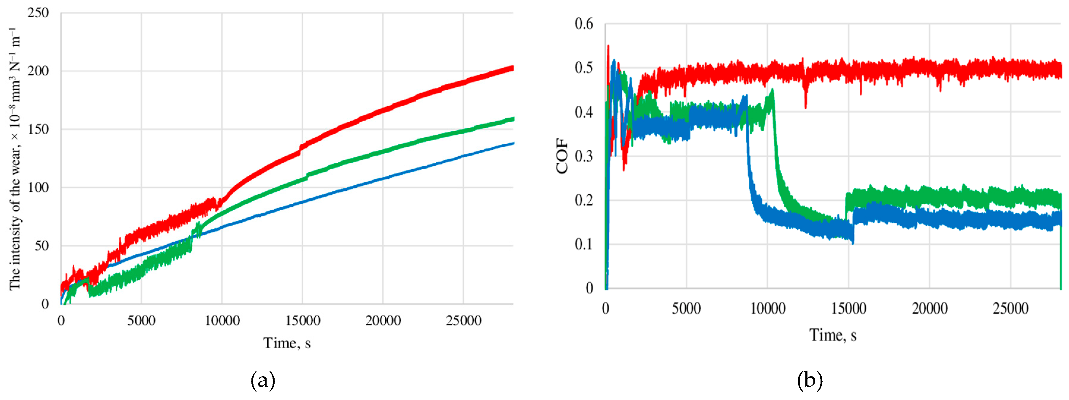
Figure 2.
Comparison results of wear resistance of samples with different HCS process parameters, as well as a sample prepared using the IB method in the pin-on-disc test.
Figure 2.
Comparison results of wear resistance of samples with different HCS process parameters, as well as a sample prepared using the IB method in the pin-on-disc test.
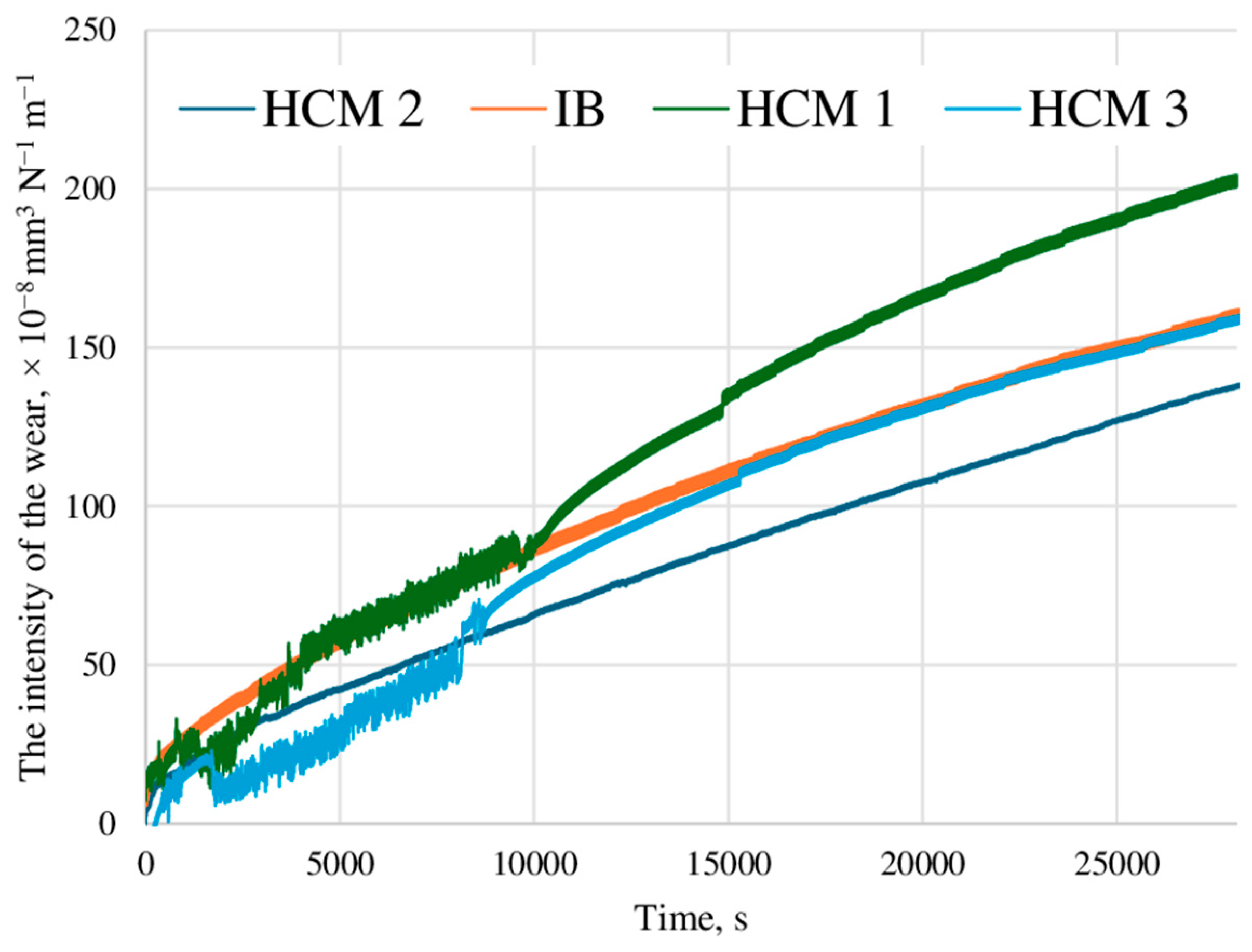
Figure 3.
Wear intensity versus bias voltage. Finding the approximating function.
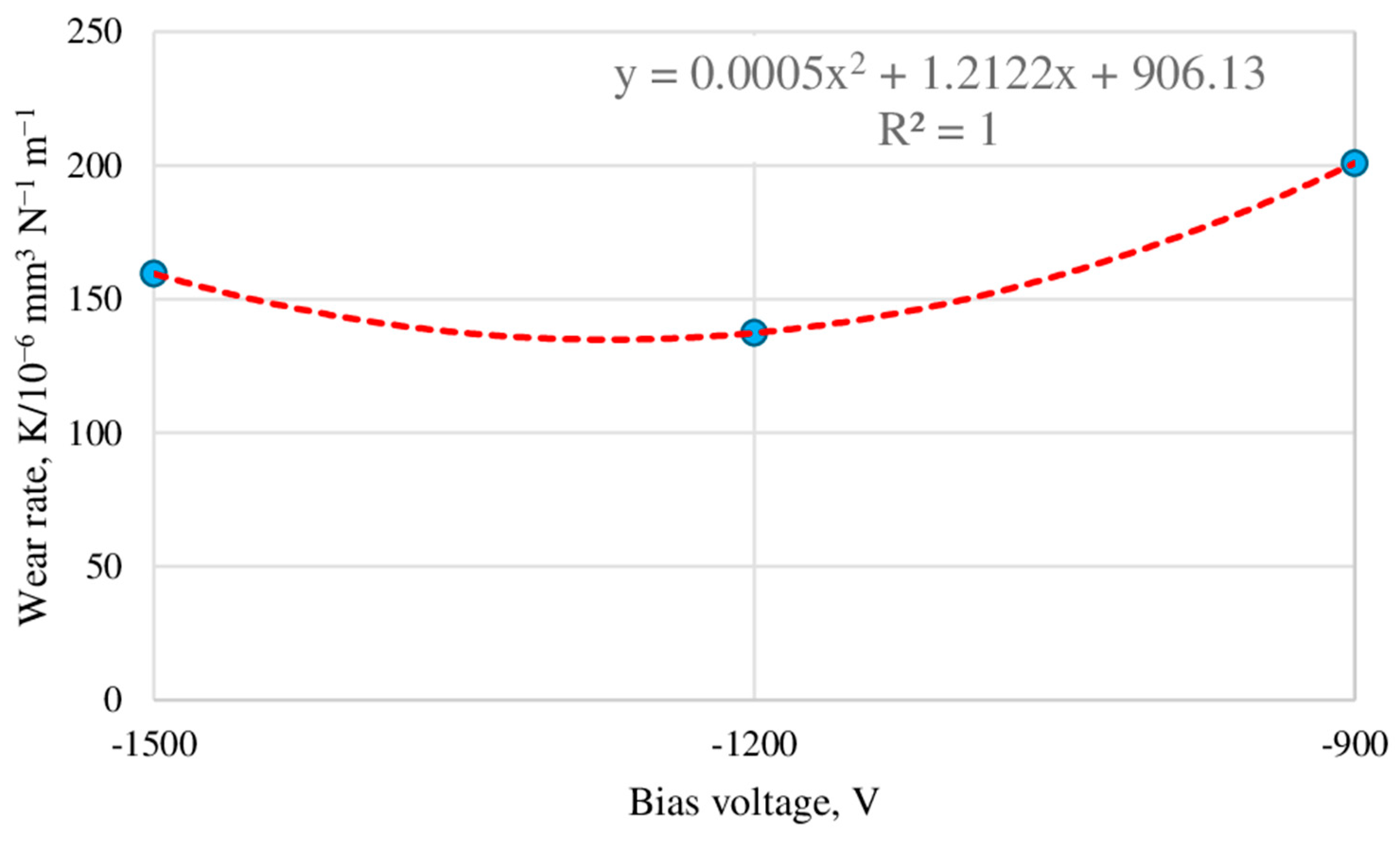
Figure 4.
General view of the worn surface of coated samples after pin-on-disc testing (optical microscope).
Figure 4.
General view of the worn surface of coated samples after pin-on-disc testing (optical microscope).
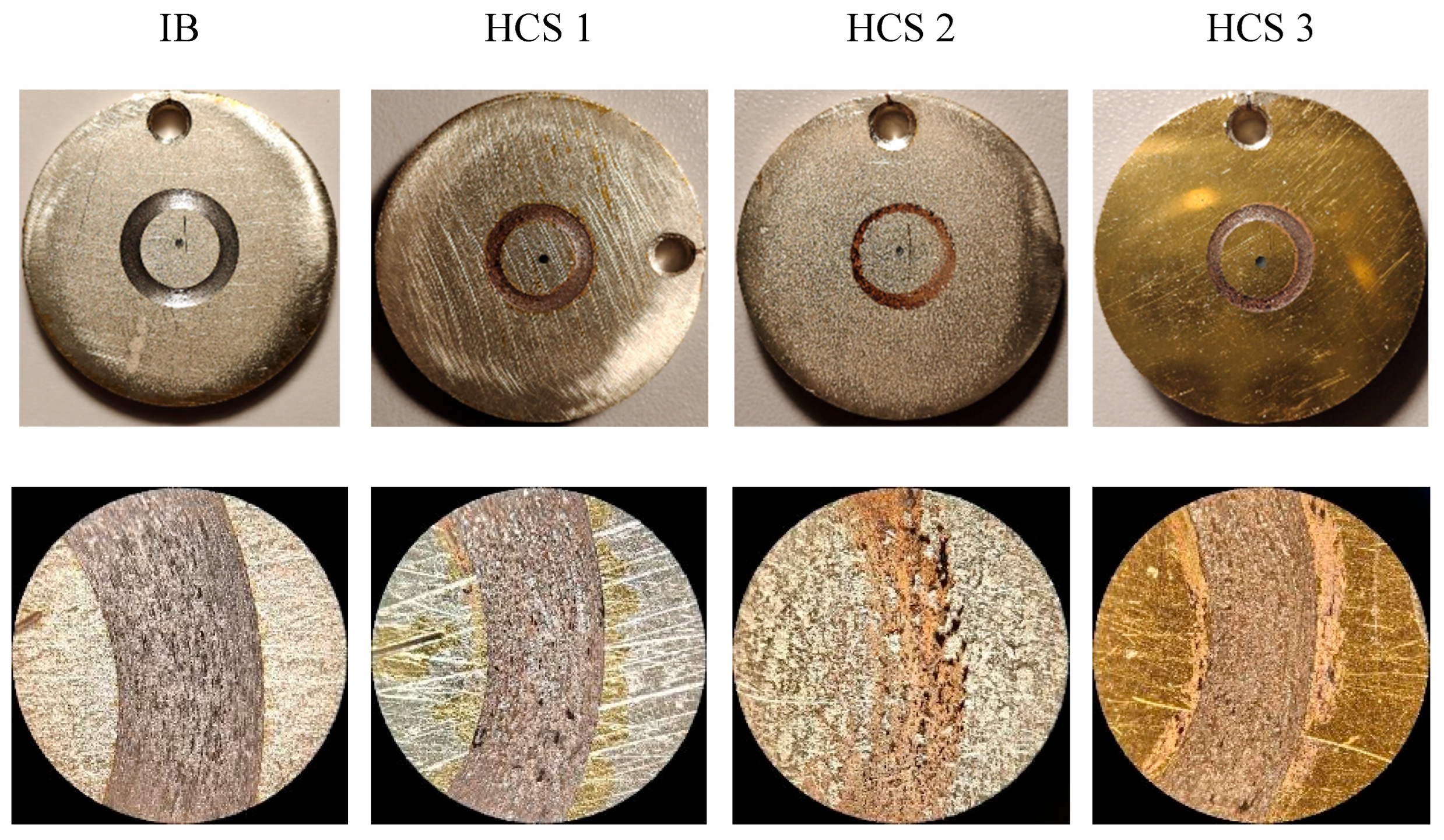
Figure 5.
Surface wear behavior of a stainless steel specimen with HCS 2 coatings in a pin-on-disc test, at magnifications of ×55 (a), ×500 (b), and ×1,000 (c).
Figure 5.
Surface wear behavior of a stainless steel specimen with HCS 2 coatings in a pin-on-disc test, at magnifications of ×55 (a), ×500 (b), and ×1,000 (c).
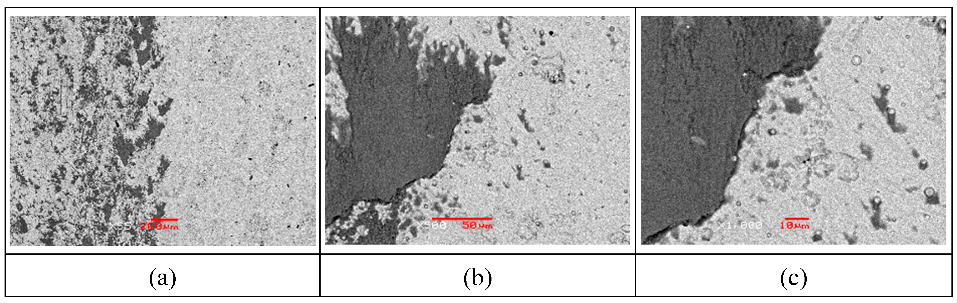
Figure 6.
Surface wear behavior of a stainless steel specimen with IB coatings in a pin-on-disc test, at magnifications of ×55 (a), ×500 (b), and ×1,000 (c).
Figure 6.
Surface wear behavior of a stainless steel specimen with IB coatings in a pin-on-disc test, at magnifications of ×55 (a), ×500 (b), and ×1,000 (c).
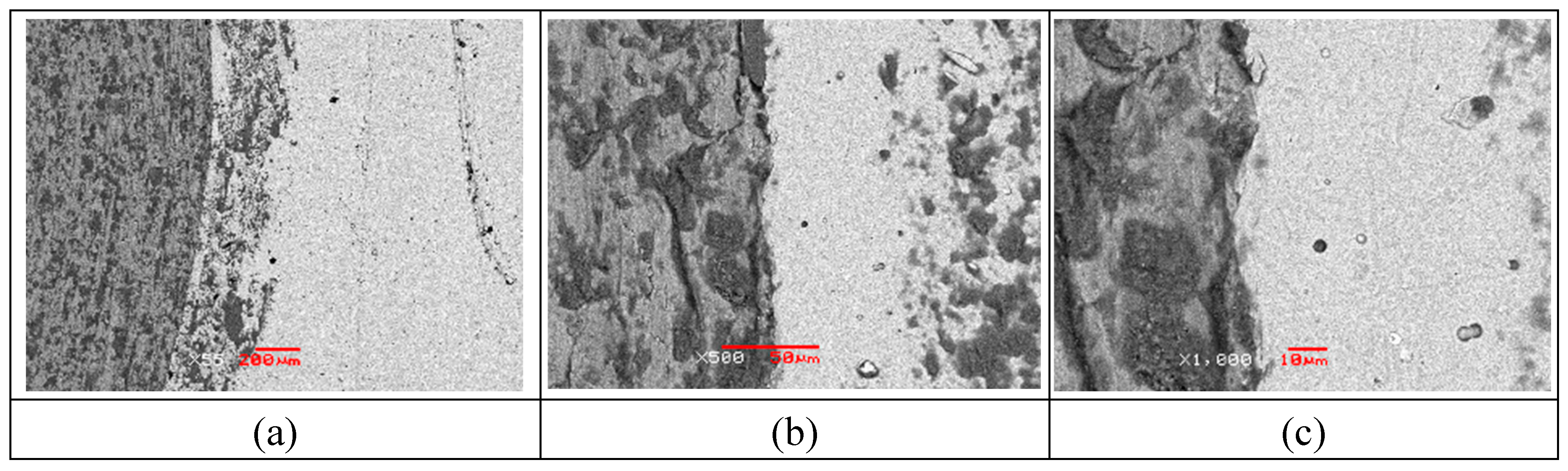
Figure 7.
Internal structure and composition of the interface layer of the HCS-coated stainless steel sample: (a-d) – interface layer structure; (e-h) – element content analysis of the interface layer.
Figure 7.
Internal structure and composition of the interface layer of the HCS-coated stainless steel sample: (a-d) – interface layer structure; (e-h) – element content analysis of the interface layer.
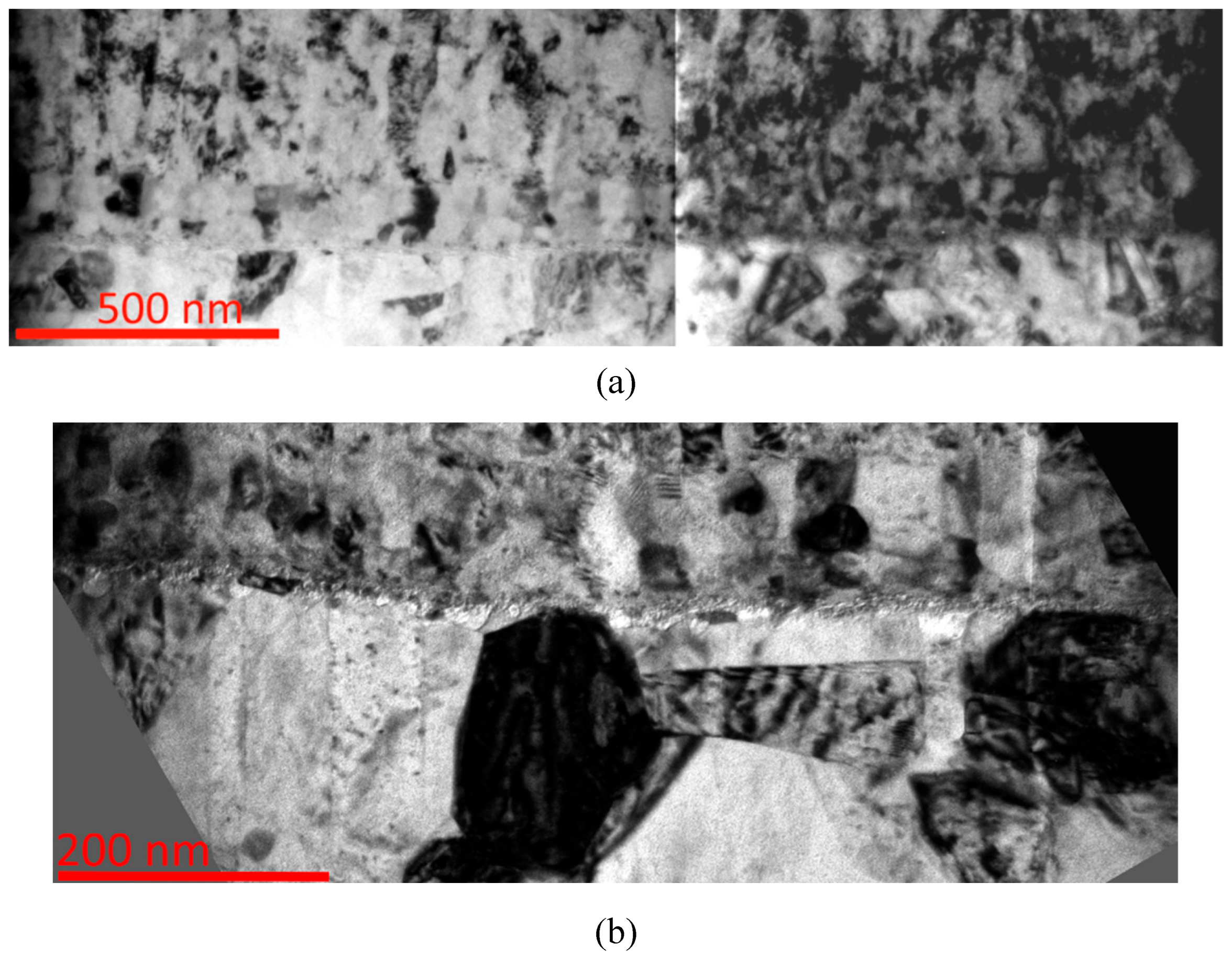
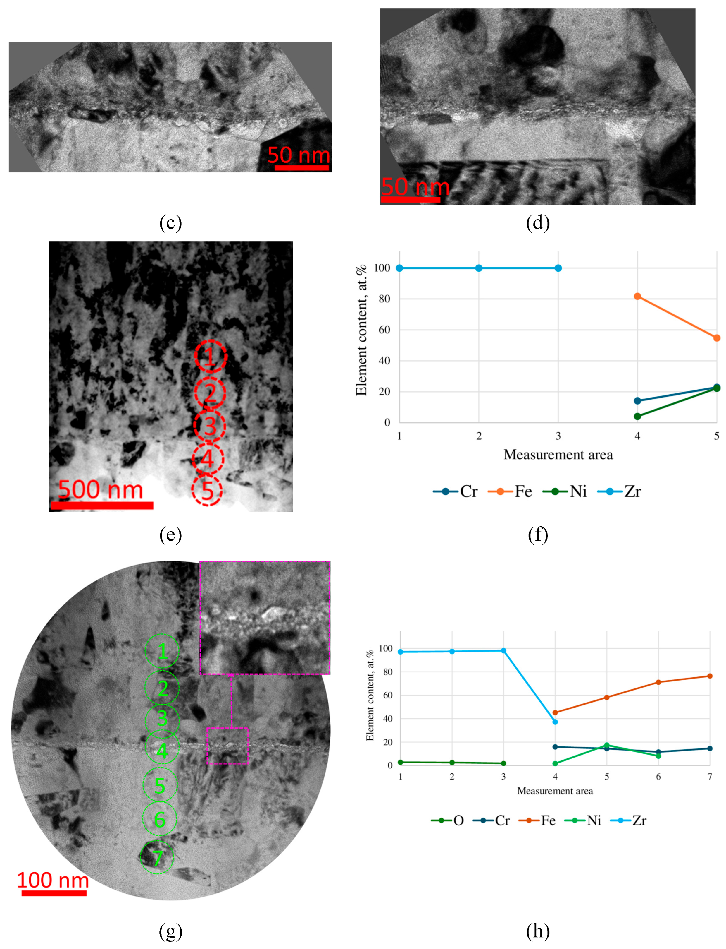
Figure 8.
Composition of the interface layer of a stainless steel sample with an HCS coating.
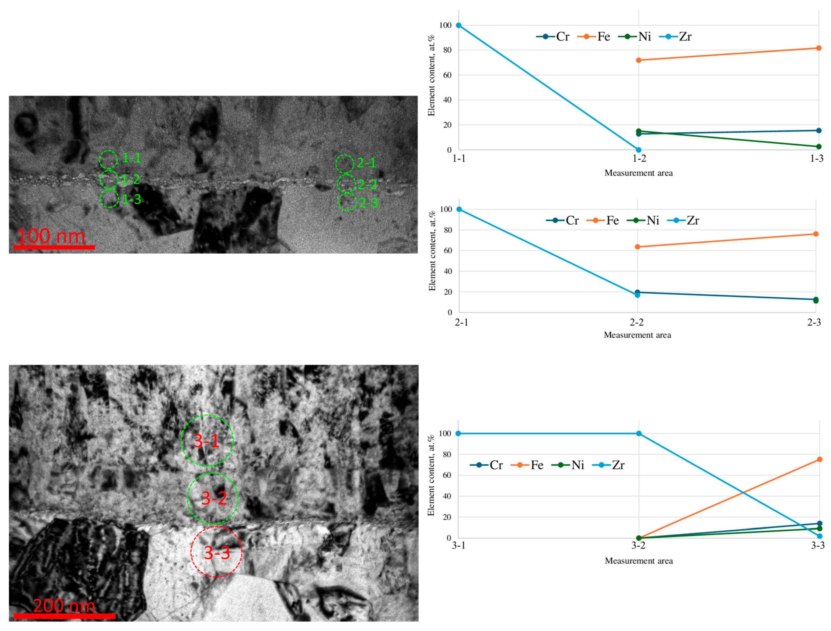
Figure 9.
Internal structure and composition of the surface layer of a stainless steel specimen with an IB coating in the pin-on-disc test: (a) – interface layer structure; (b-d) – study of the change in the element content in the direction perpendicular to the interface; (e,f) – change in the element content along the interface layer.
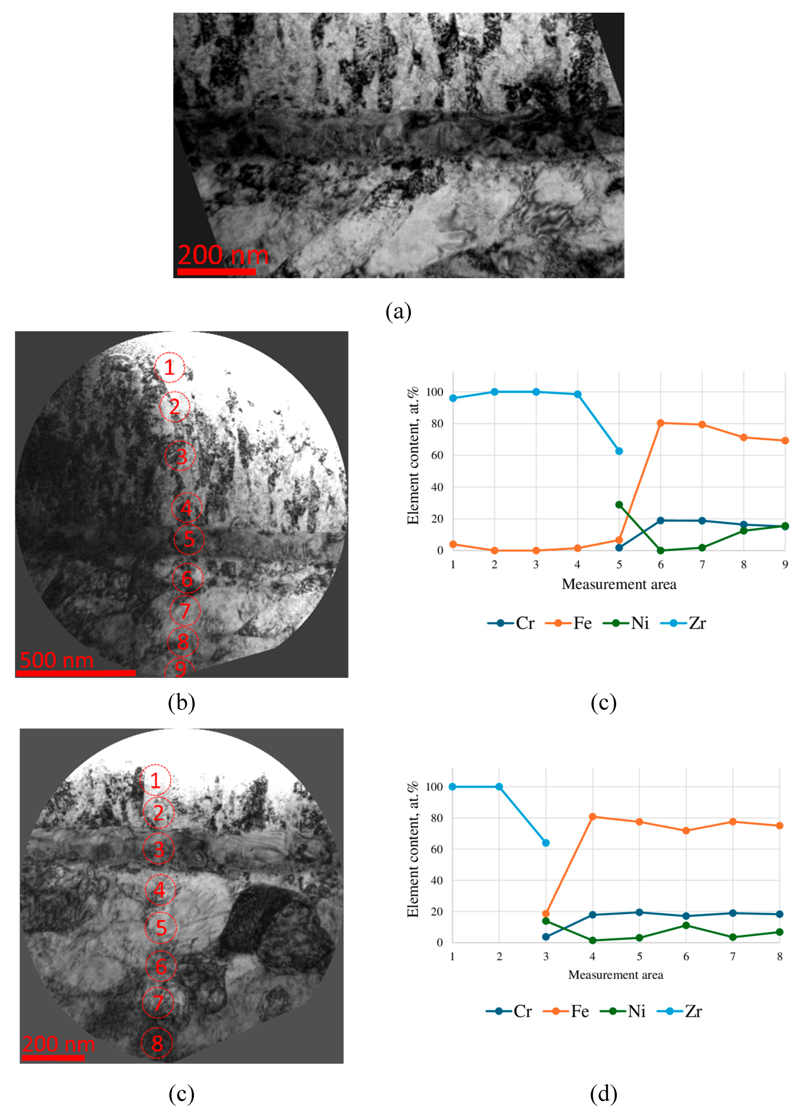
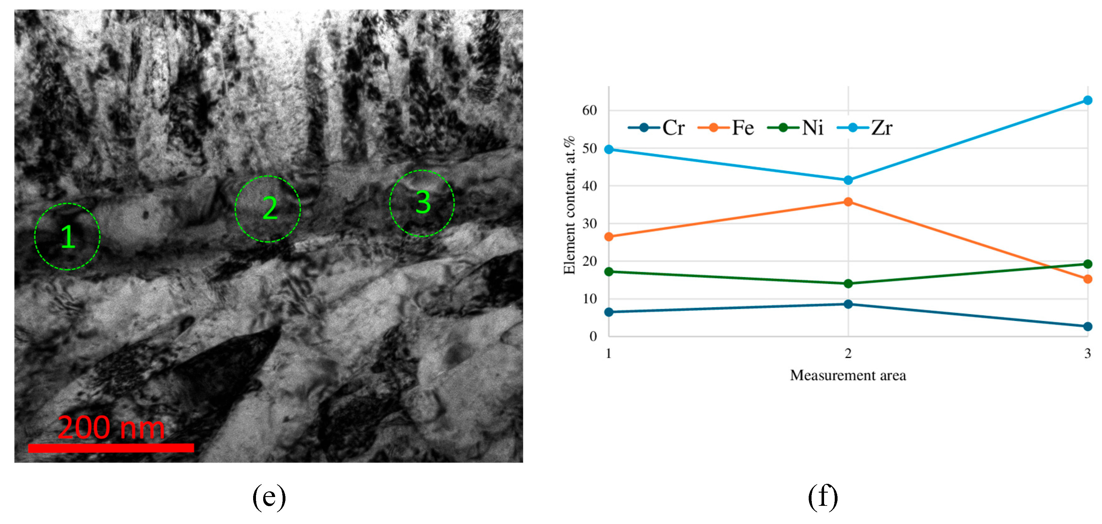
Figure 10.
Study of resistance of coated samples to destruction during scratch testing.
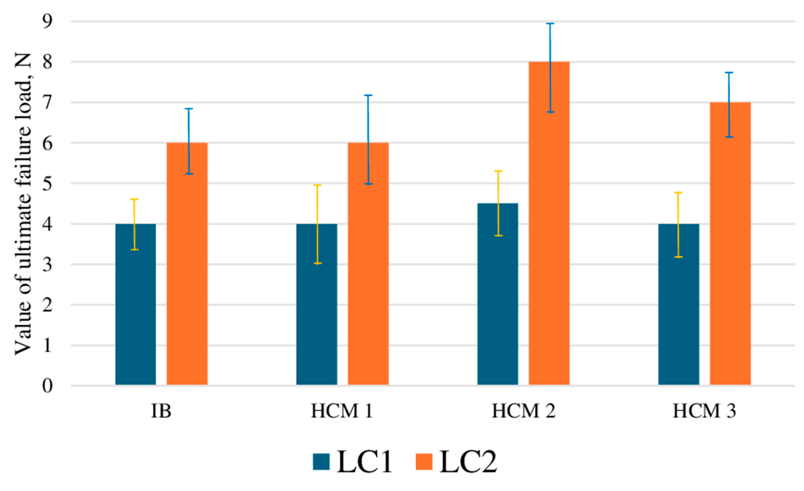
Figure 11.
Nature of destruction of HCS and IB coatings on AISI 321 steel substrate.
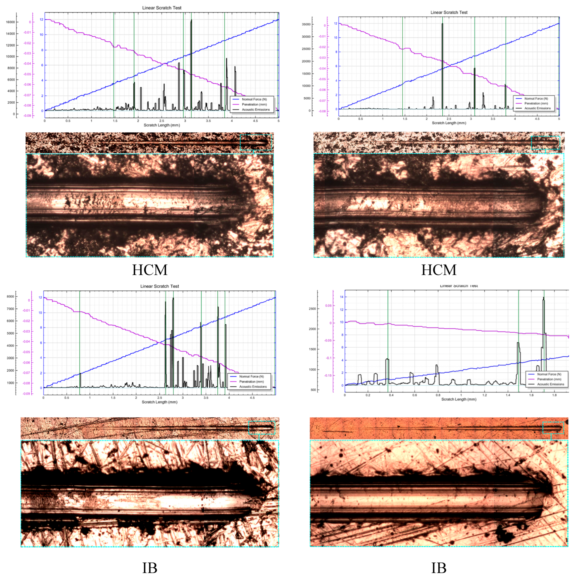

Table 1.
Designation of samples depending on the magnitude of the bias voltage on the substrate.
| Designation of samples | HCS 1 | HCS 2 | HCS 3 |
| Substrate bias voltage, V | –900 V | –1200 V | –1500 V |
Disclaimer/Publisher’s Note: The statements, opinions and data contained in all publications are solely those of the individual author(s) and contributor(s) and not of MDPI and/or the editor(s). MDPI and/or the editor(s) disclaim responsibility for any injury to people or property resulting from any ideas, methods, instructions or products referred to in the content. |
© 2025 by the authors. Licensee MDPI, Basel, Switzerland. This article is an open access article distributed under the terms and conditions of the Creative Commons Attribution (CC BY) license (http://creativecommons.org/licenses/by/4.0/).
Copyright: This open access article is published under a Creative Commons CC BY 4.0 license, which permit the free download, distribution, and reuse, provided that the author and preprint are cited in any reuse.


