Preprint
Article

This version is not peer-reviewed.

Comprehensive Spectroscopic Study of Competing Recombination Channels and Thermal Quenching Mechanisms in β-Ga2O3 Single Crystals

A peer-reviewed article of this preprint also exists.

Submitted:

07 October 2025

Posted:

08 October 2025

You are already at the latest version

Abstract

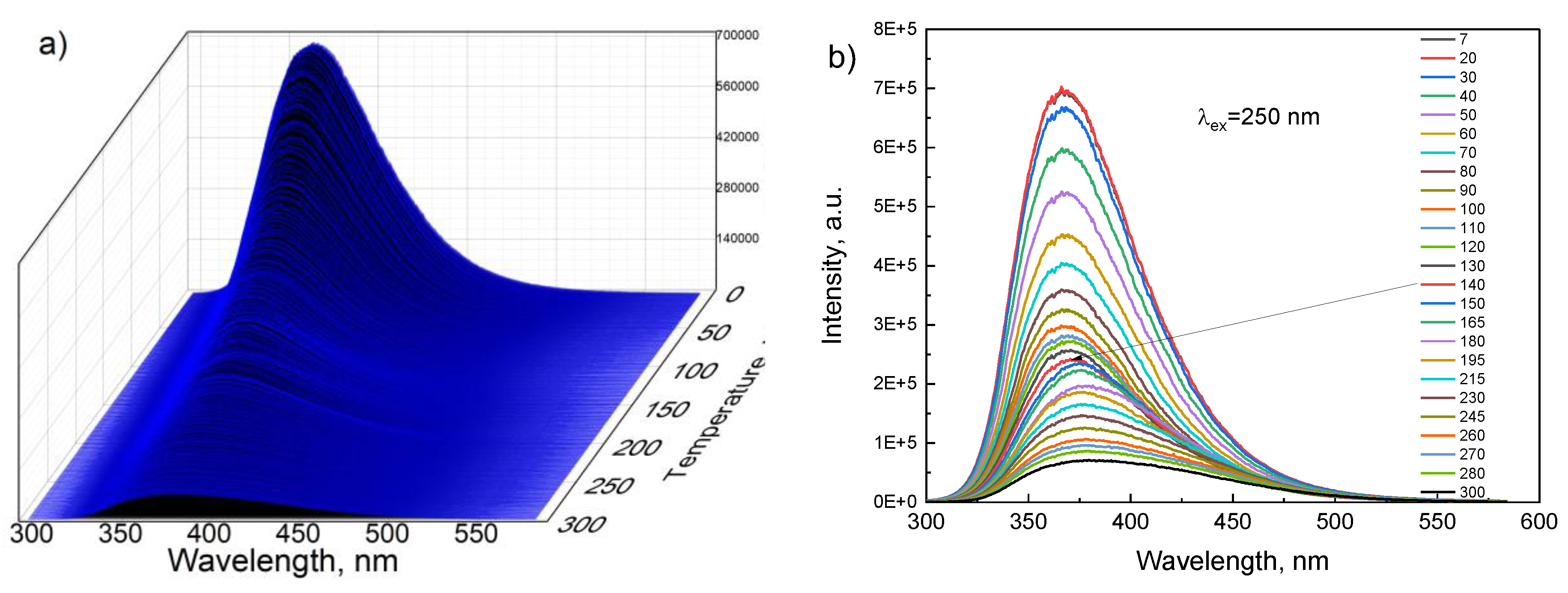
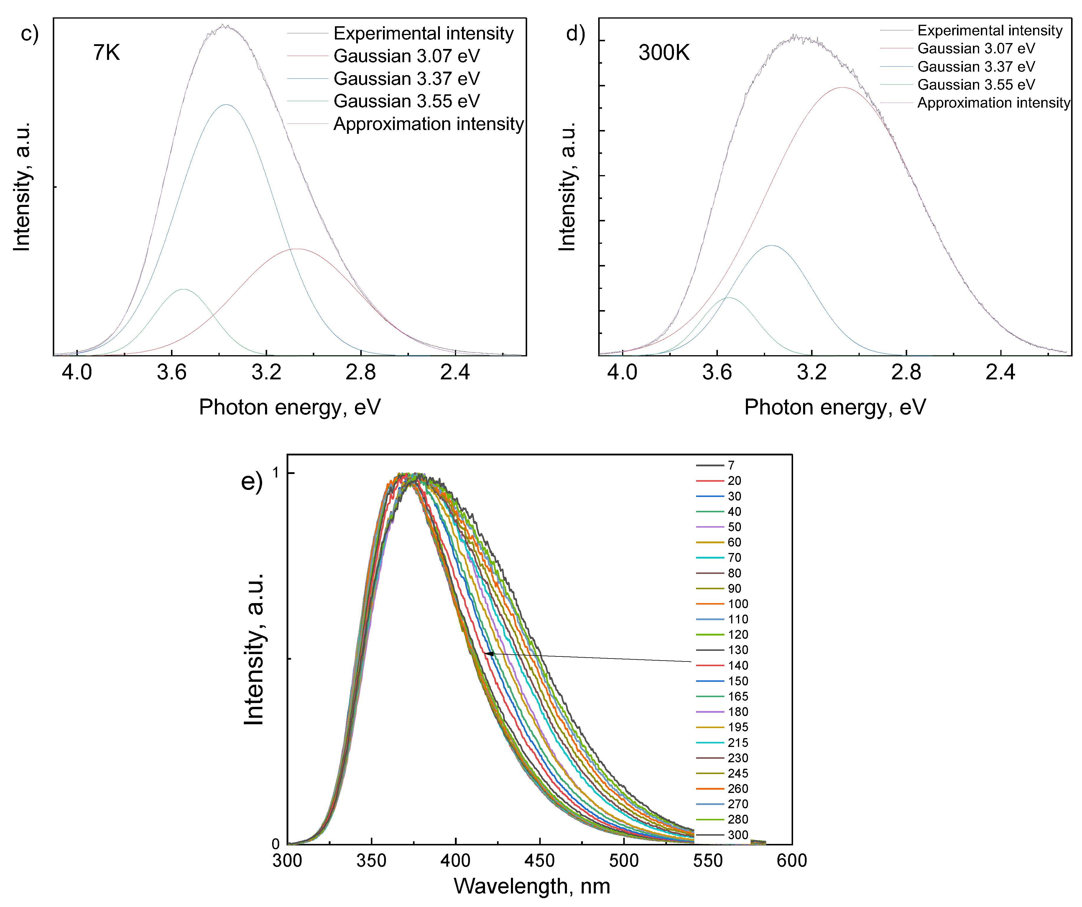
This work investigates a comprehensive temperature-dependent photoluminescence study (7–300 K) of β- Ga2O3 single crystals under 250 nm excitation. The emission consists of three competing bands at ~3.55 eV (J1), ~3.37 eV (J2), and ~3.07 eV (J3). With increasing temperature, the spectra exhibit a redshift, band broadening, and a characteristic crossover near ~140 K. A two-channel Arrhenius analysis of global thermal quenching at λmax, J1 and J2, reveals a common shallow barrier E1 =7–12 meV alongside deeper, band-specific barriers of E2=27 meV for J1 and E2=125 meV for J2. The J3 band shows a non-monotonic intensity (dip–peak–quench), reproduced by a trap-assisted generation term with a carrier-release energy Erel of order tens of meV, explaining a local maximum around ~170 K. Linewidth analysis using a single-optical-phonon model yields effective phonon energies Eph≈40–46 meV for the integral spectrum and J3, consistent with strong electron–phonon coupling; deviations for J1/J2 indicate multi-phonon and/or inhomogeneous broadening. These results establish a coherent picture of thermally driven redistribution from near-edge/STE-like states to deeper defect centers, modulated by shallow traps, and provide quantitative targets (activation and phonon energies) for defect engineering in β-Ga2O3-based optoelectronic and scintillation applications.

Keywords: 
;  ;  

1. Introduction

Gallium oxide in its thermodynamically stable monoclinic phase (β-Ga2O3) is a wide-bandgap semiconductor (Eg ≈ 4.5–4.9 eV) that has attracted considerable attention for its potential applications in power electronics [1,2,3,4], solar-blind UV photodetectors [2,5,6,7,8,9,10], luminescence detectors and scintillators [11,12,13,14,15,16,17,18,19,20], catalysts [21,22,23,24] and related sensors [25,26,27,28] and devices for micro- and nanoelectronics [29,30,31,32,33,34,35,36,37,38]. Its unique optical and electrical properties [39,40,41] are largely governed by a complex defect structure, and luminescence under various excitation methods (photoluminescence, cathodoluminescence, X-ray-excited luminescence, etc.) serves as a powerful tool to probe these defects [42]. Unlike classical semiconductors, β-Ga2O3 exhibits virtually no band-to-band (near-band-edge) emission; instead, its luminescence spectra consist of several broad bands in the UV, blue, and green spectral regions [43,44]. These emission bands are associated with intrinsic and extrinsic defect centers within the bandgap. Commonly observed are a UV or ultraviolet luminescence (UVL) band (often around 3.2–3.8 eV), a blue luminescence (BL) band (~2.8–3.0 eV), and sometimes green (GL) or other visible bands, depending on sample composition and defects [42].
Studying the temperature dependence of luminescence is a key approach to understanding the recombination mechanisms, the stability of luminescence centers, and the role of nonradiative processes in β-Ga2O3. In general, thermal quenching, i.e. the reduction of luminescence intensity with increasing temperature, is universally observed, but its specific characteristics (activation energies, quenching stages) depend on the type of luminescence (UVL, BL, etc.) and the defect makeup of the sample.
Many previous studies have examined these dependencies under various excitation conditions:
Photoluminescence (PL): Early photoluminescence studies on β-Ga2O3 single crystals showed that the blue emission band quenches in two steps: an initial quenching with a low activation energy of ~0.05 eV (attributed to thermal release of electrons from shallow donors), and a second quenching stage at higher temperatures with activation energy ~0.42 eV (attributed to release of holes from deep acceptors)[42]. Studies on Li-doped β-Ga2O3 nanostructures observed that as temperature is lowered from 300 K to 10 K, the overall luminescence intensity increases (due to suppression of thermal quenching) and a broad red-infrared emission band splits into several sharp peaks, revealing a fine structure of defect-related emission centers [45]. Temperature-resolved photoluminescence excitation (PLE) spectroscopy from 5 K to 350 K has been used to track the shift of optical transition energies in β-Ga2O3; the temperature dependence of these transitions can be described by the Varshni model, allowing extraction of fundamental parameters like the average phonon energies (17–27 meV) and the strength of electron–phonon coupling in the material [46]. In Eu-doped Ga2O3 ceramics (β-Ga2O3:Eu), a dominant “matrix” luminescence band at 300–550 nm (peaking ~440 nm) is observed at low temperatures, arising from Ga–O defect donor–acceptor pair recombination; this band rapidly loses intensity above ~100 K. Its thermal quenching follows a two-barrier behavior with activation energies E₁ ≈ 45 meV and E₂ ≈ 187 meV [47].
Cathodoluminescence (CL): Electron-beam excitation has provided detailed insight into temperature quenching associated with both intrinsic and impurity centers. CL studies on β-Ga2O3 nanowires (80–300 K) revealed that below ~220 K, in addition to the usual UVL band, a higher-energy deep-UV band (DUVL) emerges. Both the DUVL and UVL bands exhibit thermal quenching with similar activation energies of ~74–77 meV [48]. In Si-doped β-Ga2O3, cathodoluminescence over 4.5–310 K showed a two-step quenching for the UV emission band: the first stage with activation energy ~31–34 meV was attributed to thermal ionization of Si donors, and the second stage (dominant at higher T) with activation energy ~63–75 meV was attributed to the activation of a nonradiative recombination center [49]. Furthermore, analysis of CL in Si- and N-doped samples indicated two quenching components for the UVL band with activation energies of ~8.5 meV (associated with self-trapped exciton processes) and ~71 meV (associated with donor–acceptor-pair recombination), confirming the presence of multiple competing quenching pathways [50].
X-ray-excited luminescence (XEL): XEL studies (50–290 K) reinforce the general thermal quenching trends and relate them to defect migration and scintillation behavior. In β-Ga2O3 single crystals, the UV luminescence band quenches with an activation energy of ~72–90 meV. A key finding was a proposed quenching mechanism involving thermally activated migration of self-trapped holes (STH) to nonradiative recombination centers, specifically gallium vacancies (VGa-3) [51]. In crystals with different electrical conductivities, XEL revealed distinct quenching mechanisms for the blue luminescence band: in conductive samples, a quenching activation energy of ~0.48 eV was found (attributed to thermal delocalization of holes from acceptors), whereas in highly resistive samples the quenching energy was only ~0.08 eV (attributed to delocalization of electrons from donors) [52]. Using XEL to study scintillation properties, it was shown that the light yield of β-Ga2O3 can increase significantly upon cooling, reaching a maximum at ~50 K about twice the value at room temperature, demonstrating the potential of β-Ga2O3 as a cryogenic scintillator [53].
Significance of Temperature-Dependent Luminescence Studies: Both fundamentally and practically, understanding the luminescence behavior of β-Ga₂O₃ as a function of temperature is highly important. From a fundamental perspective, analysis of thermal quenching curves and spectral line broadening provides direct access to parameters such as activation energies of nonradiative processes, binding energies of excitons or carrier traps at defects, and effective phonon energies and electron–phonon coupling strengths. These data are critical for developing and validating theoretical models of the electronic and defect states in the material [54,55,56,57,58]. From an application standpoint, the thermal stability of luminescence directly impacts the performance and reliability of β-Ga2O3-based optoelectronic devices. For high-power transistors and diodes operating at elevated temperatures, understanding degradation mechanisms related to defect activation is key. In scintillation detectors, knowledge of the temperature dependence of light yield and decay times is essential for optimizing devices, especially for low-temperature applications (such as rare-event detection experiments) [53,59,60,61,62,63]. Thus, controlling and comprehending the temperature behavior of luminescence is a necessary step for further progress in deploying gallium oxide in advanced applications.
In this work, we investigate the photoluminescence of bulk β-Ga2O3 single crystals over a wide temperature range (7–300 K) using UV laser excitation. The steady-state spectral evolution characteristics are examined to elucidate the radiative recombination channels and their thermal quenching behavior. We report detailed analyses of the luminescence spectra, including multi-Gaussian decomposition of the emission bands at different temperatures, and we apply Moth and Arrhenius models with multiple activation energies to quantify the thermal quenching process. Additionally, we analyze the temperature-dependent broadening of the luminescence bands to extract the effective phonon energy coupling with the electronic excited states. The results are discussed in the context of known luminescence mechanisms in β-Ga2O3 (STE vs. DAP recombination) and compared with previously reported values in the literature.

2. Materials and Methods

Bulk β-Ga2O3 single-crystal samples with surface orientation (–201) were used in this study. The crystals (10 × 15 × 0.65 mm in size) were purchased from Novel Crystal Technology (Tamura Corp., Japan) and grown by the edge-defined film-fed growth (EFG) melt method [64]. The crystals are nominally undoped (intrinsic) and high-resistivity. Unit cell shown in Figure 1 and Table 1 summarizes the key physical characteristics of the β-Ga2O3 crystal as provided by the manufacturer. These include the monoclinic crystal structure parameters, mechanical properties, and thermal and optical constants relevant to the material.
Optical absorption measurements were performed on the β-Ga₂O₃ crystal (thickness 0.65 mm) at room temperature using a UV–Vis spectrophotometer Agilent Cary 7000 UMS (Agilent, USA). The absorption edge was analyzed using Tauc plots for both indirect and direct bandgap transitions. Photoluminescence (PL) spectra were recorded using a pulsed ultraviolet laser at 250 nm (4.96 eV photon energy, above the bandgap) as the excitation source a tunable pulsed solid-state laser (Ekspla NT342/3UV). The luminescence was detected with an Andor SR-303i-B spectrometer coupled to an Andor iStar DH734 CCD camera. Low-temperature experiments were carried out in an Advanced Research Systems DE202 N helium cold-finger cryostat. The sample was mounted in a temperature-controlled cryostat, allowing measurements from 7 K (liquid helium temperature) up to 300 K.
To analyze the composite emission bands, the spectra were deconvolved into Gaussian components using a least-squares fitting routine. This allowed identification of sub-band contributions and their evolution with temperature. The temperature dependence of the integrated luminescence intensity was analyzed using a multi-level Arrhenius model. Specifically, we assume the luminescence intensity I(T) follows an expression of the form:
I T = I 0 1 + i B i exp E i k B T ,
where I0 is the intensity in the limit of very low temperature (when thermal quenching is negligible), Ei are the activation energies of nonradiative (quenching) processes, Bi are pre-exponential constants, and kB is the Boltzmann constant [65,66,67]. Equation (1) accounts for multiple nonradiative recombination channels i that compete with the radiative luminescence. The fitting of the experimental I(T) data to this model yields the characteristic Ei and Bi parameters for the thermal quenching.
The broadening of the luminescence bands with temperature was analyzed by tracking the full width at half maximum (FWHM) of each emission component as a function of T. We employed a one-phonon coupling model to describe the homogeneous broadening, given by the expression [66,67]:
Γ T = Γ 0 + A cot h E p h 2 k B T 1
Here Γ T is the FWHM of an emission line at temperature T, Γ 0 is the residual (inhomogeneous) linewidth at low temperature, E p h is an effective phonon energy associated with the dominant phonon mode coupling to the electronic transition, and A is a coupling strength parameter proportional to the Stokes shift (related to the Huang–Rhys factor). Equation (2), which originates from the theory of temperature-dependent broadening of optical transitions in semiconductors [66,67], assumes coupling to a single effective optical phonon mode. By fitting the measured FWHM vs. T data for each luminescence band, we obtained the parameters Γ 0 , A, and E p h , as well as the fit residuals (RMSE) as a measure of goodness of fit.

3. Results

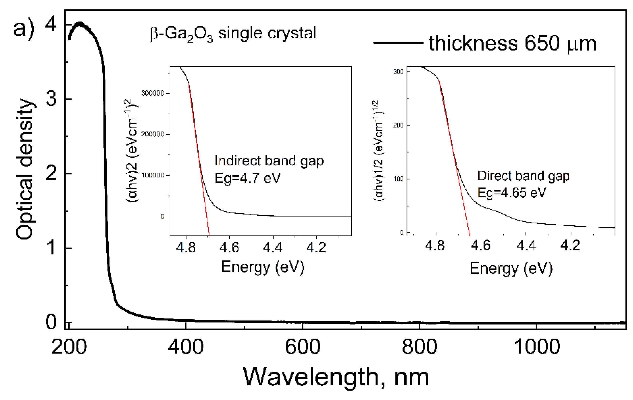
3.1. Optical Absorption and Band Gap

The β-Ga2O3 crystal shows a sharp absorption onset in the ultraviolet region. The optical density rises steeply for wavelengths shorter than 280 nm, indicating the fundamental band edge of the material in the UV range. In the visible and near-infrared range, the crystal is highly transparent (very low absorption), confirming the absence of significant mid-gap defect absorption bands and the high crystalline quality of the sample. Tauc analysis of the absorption edge was performed for both indirect and direct allowed transitions. The high-energy portion of the absorption spectrum was fitted to (αhν)1/2 vs hν (photon energy) for the indirect transition model, and to (αhν)2 vs hν for the direct transition model, where α is the absorption coefficient and hν the photon energy. From these fits, the indirect bandgap energy E g i n d was determined to be approximately 4.7 eV, while the direct bandgap E g d i r was estimated to be about 4.65 eV. This slight difference between E g i n d and E g d i r (with the indirect gap being 0.05 eV larger) indicates that β-Ga2O3 is essentially an indirect-gap semiconductor, wherein the conduction band minimum and valence band maximum occur at different k-points in the Brillouin zone. On the same sample discussed in the study, the bandgap width was evaluated using the Tauc plot method for the UID sample with a (-201) orientation, the direct bandgap values were approximately 4.85 eV with parallel polarization (0°) and 4.55 eV with perpendicular polarization (90°) [68]. For the UID sample with a (001) orientation, these values were about 4.88 eV and 4.7 eV, respectively. The obtained bandgap values are in good agreement with literature reports and electronic band structure calculations for β-Ga2O3, affirming the validity of our absorption analysis [69,70,71,72,73,74,75,76,77,78,79].
Figure 2. Absorption spectra of β-Ga2O3 single crystal. In the insert Eg obtained by Tauc method.
Preprints 179904 g002

3.2. Temperature Dependence Luminescence Spectra

The luminescent properties were investigated over a wide temperature range from 7 to 300 K (Figure 3) under pulsed laser excitation at a wavelength of 250 nm (4.96 eV), which exceeds the band gap estimated for this crystal. At low temperatures (Figure 4a–b, c), an intense broad emission band is observed in the UV–blue region with a maximum at ~3.4–3.6 eV (345–365 nm) and a pronounced asymmetric “long-tail” extension toward lower energies down to ~3.0 eV (≈410 nm and beyond).
With increasing temperature (Figure 3a–b), the overall emission intensity monotonically decreases (thermal quenching), while the maximum of the composite band shifts toward lower energies (longer wavelengths) and the band noticeably broadens. Normalized spectra (Figure 3e) emphasize two key features of the spectral evolution: (1) the persistence of an almost “isosbestic” crossing point within a narrow wavelength interval, indicative of a thermally driven redistribution of populations among a fixed set of emission channels without the emergence of new bands; and (2) a progressive enhancement of the long-wavelength tail accompanied by depletion on the short-wavelength side, reflecting the growing contribution of the low-energy channel concurrent with suppression of the UV component.
Gaussian decomposition at 7 K (Figure 3c) reveals that the spectrum is composed of at least three contributions, are well described by the sum of at least three separate bands, which will be further designated as J1, J2 and J3, with centered at energies of approximately 3.55 eV, 3.37 eV and 3.07 eV, respectively. This corresponds to the well-established emission pattern of β-Ga2O3 involving competing radiative channels: (i) a UV component at ~3.5 eV, attributed to recombination from weakly localized states (e.g., near-band-edge transitions or STE-like centers); (ii) an intermediate contribution at ~3.3–3.4 eV; and (iii) a lower-energy “blue” channel at ~3.0–3.1 eV, commonly assigned to more deeply localized defect complexes or donor–acceptor pair (DAP) recombination. At 7 K, the UV component provides a substantial share of the total emission, while the low-energy channel is present but not dominant.
Spectral fitting at 300 K (Figure 3d) quantitatively confirms this behavior: the ~3.07 eV component becomes dominant, the ~3.37 eV contribution decreases, and the high-energy ~3.55 eV component is almost completely quenched. Such spectral reshaping is consistent with a scenario of competing centers differing in localization degree and in the activation barriers for non-radiative pathways. For the more strongly localized blue centers, the radiative probability decreases only weakly with increasing temperature, whereas for high-energy channels (near-band-edge or STE-like), two thermally activated processes become significant: (i) carrier delocalization followed by trapping at non-radiative centers, and (ii) energy transfer to lower-energy defect states, which simultaneously reduces their own UV emission and channels carriers into the blue band. The additional broadening of the emission with heating reflects the strengthening of electron–phonon coupling.
From a kinetic perspective, under pulsed excitation at 250 nm (with photon energy exceeding the band gap of β-Ga2O3, the primary process involves interband transitions and excitation of strong defect-related absorption bands. This is followed by rapid carrier relaxation, which populates a set of localized states that compete with one another. Upon heating, the system enters a regime characterized by two (or more) distinct thermally activated quenching energies. Qualitatively, this manifests as a more pronounced decrease in emission intensity above ~120–150 K, accompanied by an additional enhancement of quenching toward room temperature, typical for the activation of successive nonradiative channels. Collectively, this results in (i) overall thermal quenching, (ii) a redshift of the emission maximum, (iii) an increased relative contribution of the low-energy channel, and (iv) broadening of the emission band.
Analysis of the temperature-dependent spectra indicates that around 140 K a transition point emerges, where both the spectral shape and the integral intensity begin to change simultaneously. In this region, pronounced spectral broadening becomes evident for the first time, with the long-wavelength tail strongly developing and the emission maximum gradually shifting to lower energies. Thus, 140 K can be regarded as a characteristic boundary between the low-temperature regime, dominated by near-band-edge and weakly localized radiative centers, and the high-temperature regime, where more deeply localized defects prevail and thermal quenching dominates.

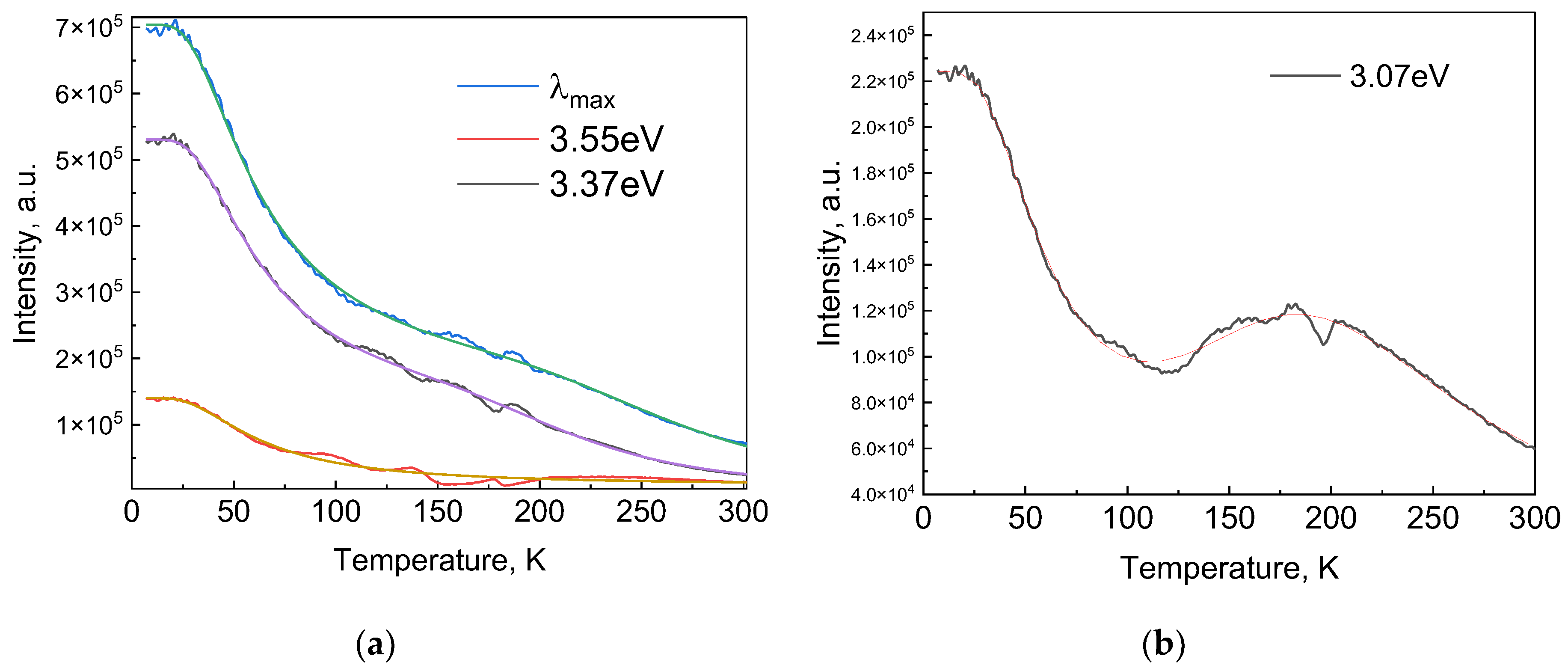
3.3. Activation Energy of Thermal Quenching

The temperature dependences at the intensity maximum (λmax) of the total spectrum, as well as for each of the three resolved bands (J1, J2, and J3), are shown in Figure 4a. For the λmax position, as well as for bands J1 and J2, the quenching curves clearly exhibit a two-step character, with a distinct change in slope around 140 K. This indicates the presence of at least two different nonradiative channels that become active at different temperatures. In contrast, band J3 shows a smoother and less pronounced quenching behavior over the entire investigated temperature range.
The results of fitting (Figure 4.) the experimental data using a two-channel thermal quenching model obtained by the expression (1) are summarized in Table 2. The analysis reveals the presence of two characteristic activation energies. The low-temperature quenching channel is characterized by an activation energy of E1 ≈ 7–12 meV and is observed for all three bands. This process becomes effective at temperatures above ~140 K. The high-temperature channel is described by an activation energy E2, which varies significantly for the different bands: 27 meV for J1 and 125 meV for J2.
Experimental data show that the intensity of the 3.07 eV band initially decreases, then exhibits a rise in the 120–180 K range, and subsequently undergoes an accelerated decrease above 200 K. Such a dip followed by a peak cannot be explained solely by the two-channel quenching model (Eq. (1)). We attribute the observed enhancement to the release of carriers from shallow traps and their subsequent capture by radiative centers. To account for this effect, we introduce a model that explicitly incorporates the contribution of traps.
Let Nt denote the density of trapped carriers in shallow traps, S the attempt frequency for their release, and Erel the energy required for transition into the conduction band or directly to a radiative center. The probability of carrier release per unit time follows the Arrhenius law:
W T   =   s exp E rel k B T ,
In the stationary regime, the released carriers increase the generation flux G by an amount ΔG(T) proportional to the exponential term. The effective generation rate therefore becomes:
G eff T = G + S exp E rel k B T ,
where S depends on both the trap density and the attempt frequency. Substituting Geff(T) into the intensity expression (1) yields the modified form:
I T = I 0 + S exp E rel k B T 1 + B 1 exp E 1 k B T + B 2 exp E 2 k B T .
Physical meaning of the modification: Erel — the thermal release energy of carriers from shallow traps; for β-Ga2O3, analysis of the 100–200 K region yields values of ~10–13 meV, in good agreement with the experimental transition; I0 — the intensity at zero temperature, determined by the concentration of radiative centers; S — the amplitude of the “trap feeding” contribution, reflecting the number of carriers that can be released.
At low temperatures (T << Erel / kB), the term s exp E rel / k B T is negligible, and Eq. (2) reduces to the classical two-channel form (Eq. (1)). In the temperature range near Erel / kB, this term enhances the numerator, leading to an increase in intensity. At sufficiently high temperatures, quenching via the high-energy channel (E2) dominates; the numerator essentially saturates, and the intensity decreases. Thermal quenching parameters obtained by using the expression (4) shown in Figure 4b and Table 3.
For the J3 band (3.07 eV), two characteristic activation barriers were identified: E1=12.6 meV (shallow quenching channel) and E2≈122.4 meV (deep channel), along with an additional energy Erel=50 meV associated with carrier release from traps. The latter accounts for the local increase in intensity observed around ≈170 K. The model does not take into account minor oscillations in intensity, which may arise from specific crystallographic trapping sites or experimental uncertainties. Nevertheless, it satisfactorily reproduces the main features of the behavior—namely, the initial decrease up to 100 K, the subsequent minimum, the intermediate maximum, and the final quenching at higher temperatures.

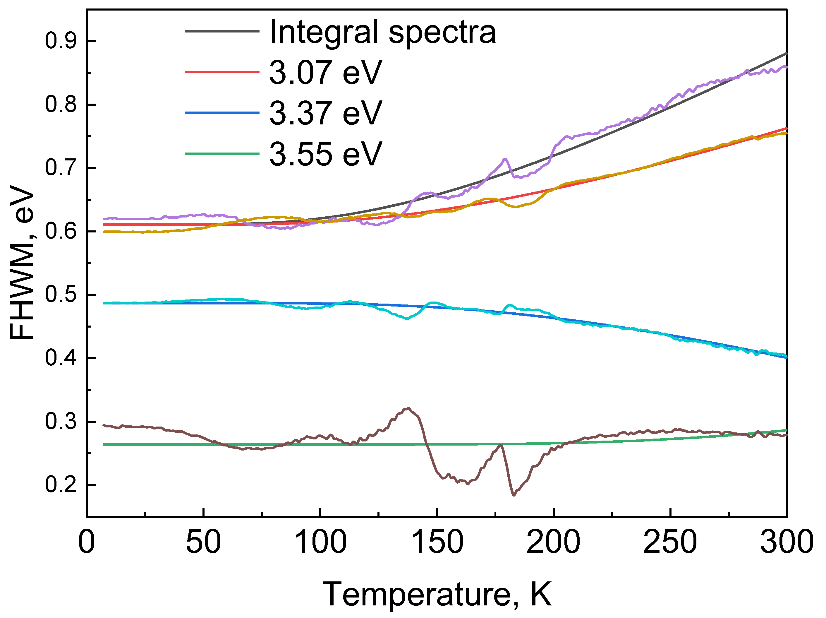
3.4. Broadening of Emission Lines

The temperature dependence of the FWHM for the integral spectrum and for the three individual components is shown in Figure 5. Overall, the width of all bands increases with temperature, which is a typical consequence of the strengthening of electron–phonon coupling. Similar to the intensity behavior, a change in the FWHM trend is observed around 140 K, where the rate of broadening increases, particularly for the integral spectrum and for band J3.
For quantitative analysis of this broadening, a single-optical-phonon interaction model was applied according to Eq. (3) (Table 4.). The results of fitting the FWHM data are summarized in Table 3. The model adequately describes the behavior of the integral spectrum and band J3, for which physically reasonable values of the effective phonon energy Eph≈40–46 meV were obtained. However, for bands J1 and J2, the simple single-phonon model proves insufficient. For band J2, the fitting yields an unphysical negative value of the coupling constant A, while for band J1, considerable deviations between the model and the experimental data are observed, indicating a more complex nature of their temperature evolution.

4. Discussion

The temperature-dependent photoluminescence (PL) spectra of the β-Ga2O3 single crystals reveal a complex emission profile dominated by a broad UV-blue band that evolves significantly from 7 K to 300 K. Gaussian decomposition identifies three primary components: J1 at ~3.55 eV, J2 at ~3.37 eV, and J3 at ~3.07 eV. These bands align with the established luminescence mechanisms in β-Ga2O3, where ultraviolet luminescence (UVL) arises from self-trapped excitons (STE) or recombination of free electrons with self-trapped holes (STH), while blue luminescence (BL) is attributed to donor-acceptor pair (DAP) recombination [42,43,51]. The high-energy J1 band (~3.55 eV) corresponds to UVL associated with weakly localized states, such as near-band-edge transitions or STE-like centers, consistent with reports of DUVL (~3.9 eV) and UVL (~3.25 eV) components linked to distinct STH configurations at different oxygen sites [18,25]. The intermediate J2 band (~3.37 eV) may represent a transitional state between STE and DAP processes, while the low-energy J3 band (~3.07 eV) is characteristic of BL from DAP involving intrinsic defects like oxygen vacancies (VO) as donors and gallium vacancies (VGa) or their complexes (VO-VGa) as acceptors [42,43,80].
The observed redshift of the emission maximum with increasing temperature, accompanied by enhanced contribution from the low-energy tail, indicates thermally driven carrier redistribution among these centers. At low temperatures, the UV component (J1) dominates due to suppressed nonradiative processes, but as temperature rises, carriers delocalize from shallow traps and transfer to deeper defect states, boosting the BL (J3) while quenching UVL. This is evidenced by the "isosbestic" point in normalized spectra, suggesting a fixed set of competing channels without new bands emerging [45]. Polarization-dependent PL studies further support this, showing anisotropic excitation of STH states that influence spectral shifts [46,81,82,83,84,85,86].
Thermal quenching analysis using the multi-channel Mott model (Eq. 1) yields activation energies E1 ≈ 7–12 meV (low-temperature channel) for all bands and E2 varying from 27 meV (J1) to 125 meV (J2 and λmax). For J3, an extended model (Eq. 4) incorporating trap release (Erel ≈ 50 meV) explains the intensity rise around 120–180 K, attributed to carrier detrapping and subsequent capture by radiative centers. These values compare favorably with literature: UVL quenching energies of 70–90 meV in CL and XEL studies, linked to STE migration over barriers to nonradiative centers like VGa-3 rather than full delocalization (binding energy ~0.5–0.9 eV) [49,50,51,65]. For BL, the higher E2 ≈ 122 meV in J3 aligns with ~0.42–0.48 eV in conductive samples (hole delocalization from acceptors) or ~0.08 eV in resistive ones (electron delocalization from donors), reflecting sample resistivity and defect makeup [42,52]. The two-step quenching in J1 and J2 mirrors reports in Si-doped samples (~31–34 meV for donor ionization, ~63–75 meV for nonradiative centers) [49,50].
The temperature-dependent FWHM broadening, fitted to the single-phonon model (Eq. 2), provides effective phonon energies Eph ≈ 40–46 meV for the integral spectrum and J3, consistent with Raman modes (~20–100 meV) and strong electron-phonon coupling (Huang-Rhys factor S ~9–39) in β-Ga2O3 [45,51,66,67]. The model's limitations for J1 and J2 (unphysical A for J2, high RMSE for J1 with Eph ≈ 124 meV) suggest additional inhomogeneous broadening or multi-phonon contributions, as seen in nanowires and doped ceramics [47,48]. The ~140 K transition in both intensity and FWHM trends marks a shift from low-T dominance of weakly localized centers to high-T prevalence of deep defects and phonon-driven processes.
These findings underscore the role of intrinsic defects in governing luminescence efficiency, with implications for optimizing β-Ga2O3 for optoelectronics and scintillators.

5. Conclusions

This comprehensive study of temperature-dependent photoluminescence in β-Ga2O3 single crystals elucidates key recombination mechanisms and thermal quenching pathways. The emission spectra decompose into three Gaussian bands (3.55 eV, 3.37 eV, 3.07 eV) attributed to STE/UVL and DAP/BL processes, with thermal redistribution favoring deeper defect states at higher temperatures. Activation energies of 7–12 meV (shallow quenching) and up to 125 meV (deep channels), plus a 50 meV trap release for the blue band, align with defect migration and delocalization models. Phonon energies of ~40–46 meV from FWHM analysis confirm strong electron-phonon interactions driving spectral broadening. These insights advance understanding of defect dynamics in β-Ga2O3, paving the way for improved device performance in high-temperature and radiation environments.

Author Contributions

Conceptualization, A.B. and A.D.; methodology, A.B., A.M.Z. and A.I.P.; formal analysis, A.D., A.M.Z., M.Ke. and A.S.; investigation, A.D., M.Ke. and M.Ko.; data curation, A.B., A.M.Z., M.Ke. and A.S.; writing—original draft preparation, A.B. and Z.T.K.; writing—review and editing, A.B., Z.T.K. and A.I.P.; visualization, M.Ko.; supervision, M.Ko. and A.I.P.; project administration, A.I.P.; resources, A.S. All authors have read and agreed to the published version of the manuscript

Funding

This research was funded by the Science Committee of the Ministry of Education and Science of the Republic of Kazakhstan (Grant No. AP23488995). In addition, Marina Konuhova and Anatoli I. Popov were supported by Latvian research project lzp-2023/1–0453 “Prediction of long-term stability of functional materials under extreme radiation conditions”.

Acknowledgments

The authors are grateful to A. Platonenko and Y. Suchikova for the fruitful discussion of the results of this work.

Conflicts of Interest

The authors declare no conflicts of interest.

References

  1. Stepanov, S.I.; Nikolaev, V.I.; Bougrov, V.E.; Romanov, A.E. Gallium Oxide: Properties and Applications—A Review. Rev. Adv. Mater. Sci. 2016, 44, 63–86. [Google Scholar]
  2. Suchikova, Y.; Nazarovets, S.; Popov, A.I. Ga2O3 solar-blind photodetectors: From civilian applications to missile detection and research agenda. Optical Materials 2024, 157, 116397. [Google Scholar] [CrossRef]
  3. Nikolaev, V.I.; Maslov, V.; Stepanov, S.I.; Pechnikov, A.I.; Krymov, V.; Nikitina, I.P.; Guzilova, L.I.; Bougrov, V.E.; Romanov, A.E. Growth and Characterization of β-Ga2O3 Crystals. J. Cryst. Growth 2017, 457, 132–136. [Google Scholar] [CrossRef]
  4. Mastro, M.A.; Kuramata, A.; Calkins, J.; Kim, J.; Ren, F.; Pearton, S.J. Perspective—Opportunities and Future Directions for Ga2O3. ECS J. Solid State Sci. Technol. 2017, 6, 356–359. [Google Scholar] [CrossRef]
  5. Suchikova, Y.; Lazarenko, A.; Kovachov, S.; Usseinov, A.; Karipbaev, Z.; Popov, A.I. Formation of porous Ga2O3/GaAs layers for electronic devices. In Proceedings of the 2022 IEEE 16th International Conference on Advanced Trends in Radioelectronics, Telecommunications and Computer Engineering (TCSET), Lviv-Slavske, Ukraine, 2022; pp. 01–04. [Google Scholar] [CrossRef]
  6. Xiao, Z.; Chen, H.; Ning, H.; Luo, D.; Fang, X.; Li, M.; Su, G.; He, H.; Yao, R.; Peng, J. Self-Powered Ultraviolet Photodetectors Based on Conductive Polymers/Ga2O3 Heterojunctions: A Review. Polymers 2025, 17, 1384. [Google Scholar] [CrossRef]
  7. Koishybayeva, Z.; Konusov, F.; Pavlov, S.; Sidelev, D.; Nassyrbayev, A.; Gadyrov, R.; Tarbokov, V.; Polisadova, E.; Akilbekov, A. Modification of optical and photoelectrical properties of thin gallium oxide films by intense pulsed 200 keV C+ ion beams. Optical Materials: X 2025, 25, 100399. [Google Scholar] [CrossRef]
  8. Suchikova, Y.; Kovachov, S.; Bohdanov, I.; Drozhcha, D.; Kosogov, I.; Karipbayev, Z.T.; Popov, A.I. Synthesis and characterization of β-Ga2O3/por-GaAs/mono-GaAs heterostructures for enhanced portable solar cells. Physics and Chemistry of Solid State 2024, 25, 546–552. [Google Scholar] [CrossRef]
  9. Choudhury, A.; Biswas, I.; Gupta, R.; Dey, A.; Mondal, A. GLAD synthesized Ga2O3 nanowire-based photodiode. Applied Physics A 2024, 130, 752. [Google Scholar] [CrossRef]
  10. Suchikova, Y.; Kovachov, S.; Karipbaev, Z.; Zhydachevskyy, Y.; Lysak, A.; Popov, A.I. Synthesis of CdO/por-CdS/CdS Heterostructure with Doughnut-Like Crystallites. In Proceedings of the 2023 IEEE 4th KhPI Week on Advanced Technology (KhPIWeek), Kharkiv, Ukraine, 2023; pp. 1–5. [Google Scholar] [CrossRef]
  11. von Wenckstern, H. Group-III Sesquioxides: Growth, Physical Properties and Devices. Adv. Electron. Mater. 2017, 3, 1600350. [Google Scholar] [CrossRef]
  12. Drozdowski, W.; Makowski, M.; Witkowski, M.E.; Wojtowicz, A.J.; Galazka, Z.; Irmscher, K.; Schewski, R. β-Ga2O3:Ce as a Fast Scintillator: An Unclear Role of Cerium. Radiat. Meas. 2019, 121, 49–53. [Google Scholar] [CrossRef]
  13. Li, W.; Zhao, X.; Zhi, Y.; Zhang, X.; Chen, Z.; Chu, X.; Yang, H.; Wu, Z.; Tang, W. Fabrication of Cerium-Doped β-Ga2O3 Epitaxial Thin Films and Deep Ultraviolet Photodetectors. Appl. Opt. 2018, 57, 538. [Google Scholar] [CrossRef]
  14. Luchechko, A.; Vasyltsiv, V.; Zhydachevskyy, Y.; Kushlyk, M.; Ubizskii, S.; Suchocki, A. Luminescence Spectroscopy of Cr3+ Ions in Bulk Single Crystalline β-Ga2O3. J. Phys. D Appl. Phys. 2020, 53, 354001. [Google Scholar] [CrossRef]
  15. Yanagida, T.; Okada, G.; Kato, T.; Nakauchi, D.; Yanagida, S. Fast and high light yield scintillation in the Ga2O3 semiconductor material. Applied Physics Express 2016, 9, 042601. [Google Scholar] [CrossRef]
  16. Luchechko, A.; Vasyltsiv, V.; Kostyk, L.; Tsvetkova, O.; Popov, A.I. Shallow and deep trap levels in X-ray irradiated β-Ga2O3: Mg. Nucl. Instrum. Methods Phys. Res. Sect. B: Beam Interact. Mater. At. 2019, 441, 12–17. [Google Scholar] [CrossRef]
  17. Koishybayeva, Z.; Konusov, F.; Pavlov, S.; Sidelev, D.; Nassyrbayev, A.; Cheshev, D.; Gadyrov, R.; Tarbokov, V.; Akilbekov, A. Influence of short-pulsed Ion irradiation on optical and photoelectrical properties of thin gallium oxide films. Optical Materials: X 2025, 25, 100394. [Google Scholar] [CrossRef]
  18. Luchechko, A.; Vasyltsiv, V.; Kushlyk, M.; Syvorotka, I.; Kostyk, L.; Slobodzyan, D.; Zhydachevskyy, Y. Luminescence and thermally stimulated conductivity of polycrystalline β-Ga2O3: Mn and β-Ga2O3: Mn, Si. Journal of Vacuum Science & Technology A 2025, 43, 042802. [Google Scholar]
  19. Khartsev, S.; Hammar, M.; Nordell, N.; Zolotarjovs, A.; Purans, J.; Hallén, A. Reverse-Bias Electroluminescence in Er-Doped β-Ga2O3 Schottky Barrier Diodes Manufactured by Pulsed Laser Deposition. physica status solidi (a) 2022, 219, 2100610. [Google Scholar] [CrossRef]
  20. Ono, R.; Kodaira, A.; Tokunaga, T.; Yoshida, H.; Yamamoto, T. A technique to modify the photoluminescence intensity of β-Ga2O3 polycrystals using an electric field during sintering. Journal of Luminescence 2023, 254, 119508. [Google Scholar] [CrossRef]
  21. Snetkov, P.P.; Morozkina, S.N.; Sosnin, I.M.; Bauman, D.A.; Hussainova, I.; Romanov, A.E. Electrospinning as a Method for Fabrication of Nanofibrous Photocatalysts Based on Gallium Oxide. physica status solidi (a) 2025, 222, 2400669. [Google Scholar] [CrossRef]
  22. Xue, R.; Zhang, J.; Liu, H.; Guan, Y.; Ha, S. Photoelectric Properties of the g-ZnO/β-Ga2O3 Heterojunction. physica status solidi (b) 2025, 262, 2400595. [Google Scholar] [CrossRef]
  23. Kondo, R.; Shimazoe, K.; Nishinaka, H. Alloying Ga2O3 with Fe2O3 on Corundum-Structured rh-ITO by Mist CVD and Its Demonstration of Photodetector and Photoelectrode Applications. physica status solidi (b) 2025, 262, 2400441. [Google Scholar] [CrossRef]
  24. Kim, S.; Park, J.H.; Kim, H.W.; Jeon, D.W.; Hwang, W.S. Comparative study of photoinduced wettability and photocatalytic activity in different crystalline Ga2O3 phases. Materials Science in Semiconductor Processing 2024, 175, 108289. [Google Scholar] [CrossRef]
  25. Nikolskaya, A.; Okulich, E.; Korolev, D.; Stepanov, A.; Nikolichev, D.; Mikhaylov, A.; Tetelbaum, D.; Almaev, A.; Bolzan, C.A.; Buaczik, A.; et al. Ion implantation in β-Ga2O3: Physics and technology. J. Vac. Sci. Technol. A 2021, 39, 030802. [Google Scholar] [CrossRef]
  26. Almaev, A.; Nikolaev, V.; Butenko, P.; Stepanov, S.; Pechnikov, A.; Yakovlev, N.; Sinyugin, I.; Shapenkov, S.; Scheglov, M. Gas sensors based on pseudohexagonal phase of gallium oxide. Phys. Status Solidi B 2021, 259, 2100306. [Google Scholar] [CrossRef]
  27. Almaev, A.; Yakovlev, N.; Kopyev, V.; Nikolaev, V.; Butenko, P.; Deng, J.; Pechnikov, A.; Korusenko, P.; Koroleva, A.; Zhizhin, E. High Sensitivity Low-Temperature Hydrogen Sensors Based on SnO2/κ(ε)-Ga2O3:Sn Heterostructure. Chemosensors 2023, 11, 32. [Google Scholar] [CrossRef]
  28. Almaev, A.; Nikolaev, V.; Yakovlev, N.; Butenko, P.; Stepanov, S.; Pechnikov, A.; Scheglov, M.; Chernikov, E. Hydrogen sensors based on Pt/α-Ga2O3:Sn/Pt structures. Sens. Actuators B Chem. 2022, 364, 131904. [Google Scholar] [CrossRef]
  29. Butanovs, E.; Zubkins, M.; Nedzinskas, R.; Zadin, V.; Polyakov, B. Comparison of two methods for one-dimensional Ga2O3-ZnGa2O4 core–shell heterostructure synthesis. Journal of Crystal Growth 2023, 618, 127319. [Google Scholar] [CrossRef]
  30. Khartsev, S.; Nordell, N.; Hammar, M.; Purans, J.; Hallén, A. High-Quality Si-Doped β-Ga2O3 Films on Sapphire Fabricated by Pulsed Laser Deposition. physica status solidi (b) 2021, 258, 2000362. [Google Scholar] [CrossRef]
  31. Zubkins, M.; Vibornijs, V.; Strods, E.; Butanovs, E.; Bikse, L.; Ottosson, M.; Hallén, A.; Gabrusenoks, J.; Purans, J.; Azens, A. Deposition of Ga2O3 Thin Films by Liquid Metal Target Sputtering. Vacuum 2023, 209, 111789. [Google Scholar] [CrossRef]
  32. Butanovs, E.; Dipane, L.; Zolotarjovs, A.; Vlassov, S.; Polyakov, B. Preparation of functional Ga2S3 and Ga2Se3 shells around Ga2O3 nanowires via sulfurization or selenization. Optical Materials 2022, 131, 112675. [Google Scholar] [CrossRef]
  33. Dimitrocenko, L.; Strikis, G.; Polyakov, B.; Bikse, L.; Oras, S.; Butanovs, E. The effect of a nucleation layer on morphology and grain size in MOCVD-grown β-Ga2O3 thin films on C-plane sapphire. Materials 2022, 15, 8362. [Google Scholar] [CrossRef]
  34. Yakovlev, N.N.; Almaev, A.V.; Kushnarev, B.O.; Verkholetov, M.G.; Poliakov, M.V.; Zinovev, M.M. β-Ga2O3 Schottky Barrier Diode with Ion Beam Sputter-Deposited Semi-Insulating Layer. Crystals 2024, 14, 123. [Google Scholar] [CrossRef]
  35. Zachinskis, A.; Grechenkov, J.; Butanovs, E.; Platonenko, A.; Piskunov, S.; Popov, A.I.; Purans, J.; Bocharov, D. Ir impurities in α- and β-Ga2O3 and their detrimental effect on p-type conductivity. Sci. Rep. 2023, 13, 8522. [Google Scholar] [CrossRef]
  36. Osipov, A.V.; Sharofidinov, S.S.; Osipova, E.V.; Kandakov, A.V.; Ivanov, A.Y.; Kukushkin, S.A. Growth and Optical Properties of Ga2O3 Layers of Different Crystalline Modifications. Coatings 2022, 12, 1802. [Google Scholar] [CrossRef]
  37. Khartsev, S.; Sarakovskis, A.; Grinberga, L.; Hammar, M.; Nordell, N.; Hallén, A. Electrical and Optical Properties of a Cu2O/β-Ga2O3 pn-Junction. physica status solidi (a) 2024, 221, 2300958. [Google Scholar] [CrossRef]
  38. Suchikova, Y.; Kovachov, S.; Bohdanov, I.; Kosogov, I.; Drozhcha, D.; Popov, A.I. Design and structural characteristics of Ga2O3/por-GaAs/mono-GaAs Heterostructures for Advanced MEMS Applications. In Proceedings of the 2024 IEEE 19th Intern Conf on the Perspective Technologies and Methods in MEMS Design (MEMSTECH), Ukraine, 2024; pp. 48–51. [Google Scholar] [CrossRef]
  39. Mohamed, M.; Janowitz, C.; Unger, I.; Manzke, R.; Galazka, Z.; Uecker, R.; Fornari, R.; Weber, J.R.; Varley, J.B.; Van de Walle, C.G. The electronic structure of β−Ga2O3. Appl. Phys. Lett. 2010, 97, 211903. [Google Scholar] [CrossRef]
  40. Varley, J.B.; Schleife, A. Bethe–Salpeter Calculation of Optical-Absorption Spectra of In2O3 and Ga2O3. Semicond. Sci. Technol. 2015, 30, 024010. [Google Scholar] [CrossRef]
  41. Yamaguchi, K. First principles study on electronic structure of β-Ga2O3. Solid state communications 2004, 131, 739–744. [Google Scholar] [CrossRef]
  42. Binet, L.; Gourier, D. Origin of the blue luminescence of β-Ga2O3. J. Phys. Chem. Solids 1998, 59, 1241–1249. [Google Scholar] [CrossRef]
  43. Onuma, T.; Fujioka, S.; Yamaguchi, T.; Higashiwaki, M.; Sasaki, K.; Masui, T.; Honda, T. Correlation between blue luminescence intensity and resistivity in β-Ga2O3 single crystals. Appl. Phys. Lett. 2013, 103, 041910. [Google Scholar] [CrossRef]
  44. Usseinov, A.B.; Karipbayev, Z.T.; Purans, J.; Kakimov, A.B.; Bakytkyzy, A.; Zhunusbekov, A.M.; Koketai, T.A.; Kozlovskyi, A.L.; Suchikova, Y.; Popov, A.I. Study of β-Ga2O3 Ceramics Synthesized under Powerful Electron Beam. Materials 2023, 16, 6997. [Google Scholar] [CrossRef]
  45. Jiang, J.; Zhang, J. Temperature-resolved photoluminescence, Raman and electrical properties of Li doped Ga₂O₃ nanostructure. Ceram. Int. 2020, 46, 2409–2412. [Google Scholar] [CrossRef]
  46. Meißner, M.; Bernhardt, N.; Nippert, F.; Janzen, B.M.; Galazka, Z.; Wagner, M.R. Anisotropy of optical transitions in β-Ga2O3 investigated by polarized photoluminescence excitation spectroscopy. Appl. Phys. Lett. 2024, 124, 152102. [Google Scholar] [CrossRef]
  47. Kumarbekov, K.K.; Kakimov, A.B.; Karipbayev, Z.T.; Kassymzhanov, M.T.; Brik, M.G.; Ma, C.-g.; Piasecki, M.; Suchikova, Y.; Kemere, M.; Konuhova, M. Temperature-dependent luminescence of europium-doped Ga2O3 ceramics. Opt. Mater. X 2025, 25, 100392. [Google Scholar] [CrossRef]
  48. Chowdhury, T.; Paul, D.K.; Rahaman, M.R.; Ton-That, C.; Rahman, M.A. Temperature-dependent broadening of spectral lineshapes and kinetics of luminescence centers in monoclinic gallium oxide nanowires. J. Alloys Compd. 2025, 1010, 177609. [Google Scholar] [CrossRef]
  49. Modak, S.; Chernyak, L.; Schulte, A.; Xian, M.; Ren, F.; Pearton, S.J.; Ruzin, A.; Kosolobov, S.S.; Drachev, V.P. Temperature dependence of cathodoluminescence emission in irradiated Si-doped β-Ga2O3. AIP Adv. 2021, 11, 125014. [Google Scholar] [CrossRef]
  50. Onuma, T.; Nakata, Y.; Sasaki, K.; Masui, T.; Yamaguchi, T.; Honda, T.; Kuramata, A.; Yamakoshi, S.; Higashiwaki, M. Modeling and interpretation of UV and blue luminescence intensity in β-Ga2O3 by silicon and nitrogen doping. J. Appl. Phys. 2018, 124, 075103. [Google Scholar]
  51. Tang, H.; He, N.; Zhu, Z.; Gu, M.; Liu, B.; Xu, J.; Xu, M.; Chen, L.; Liu, J.; Ouyang, X. Temperature-dependence of X-ray excited luminescence of β-Ga2O3 single crystals. Appl. Phys. Lett. 2019, 115, 071904. [Google Scholar] [CrossRef]
  52. Vasyltsiv, V.; Kostyk, L.; Tsvetkova, O.; Lys, R.; Kushlyk, M.; Pavlyk, B.; Luchechko, A. Luminescence and Conductivity of β-Ga2O3 and β-Ga2O3:Mg Single Crystals. Acta Phys. Pol. A 2022, 141, 312–317. [Google Scholar]
  53. Mykhaylyk, V.B.; Kraus, H.; Kapustianyk, V.; Rudko, M. Low temperature scintillation properties of Ga2O3. Appl. Phys. Lett. 2019, 115, 081103. [Google Scholar] [CrossRef]
  54. Galazka, Z. β-Ga2O3 for wide-bandgap electronics and optoelectronics. Semiconductor Science and Technology 2018, 33, 113001. [Google Scholar]
  55. Makeswaran, N.; Das, D.; Zade, V.; Gaurav, P.; Shutthanandan, V.; Tan, S.; Ramana, C.V. Size-and phase-controlled nanometer-thick β-Ga2O3 films with green photoluminescence for optoelectronic applications. ACS Applied Nano Materials 2021, 4, 3331–3338. [Google Scholar]
  56. Islam, M.M.; Rana, D.; Hernandez, A.; Haseman, M.; Selim, F.A. Study of trap levels in β-Ga2O3 by thermoluminescence spectroscopy. Journal of Applied Physics 2019, 125, 055701. [Google Scholar] [CrossRef]
  57. Zatsepin, A.F.; Buntov, E.A.; Pustovarov, V.A. Luminescenсe of nanoparticles and quantum dots in Zn, Mn-implanted silica layers. Optical Materials 2025, 159, 116675. [Google Scholar] [CrossRef]
  58. Popov, A.I.; Balanzat, E. Low temperature X-ray luminescence of KNbO3 crystals. Nuclear Instruments and Methods in Physics Research Section B: Beam Interactions with Materials and Atoms 2000, 166, 305–308. [Google Scholar] [CrossRef]
  59. Lisitsyn, V.M.; Bikhert, Y.V.; Lisitsyna, L.A.; Dauletbekova, A.K.; Reyterov, V.M.; Karipbayev, Z.T. Cathodoluminescence and Radiation-Induced Absorption in YLiF4 Crystals in Excitation by Electron Pulse. Advanced Materials Research 2014, 880, 13–18. [Google Scholar] [CrossRef]
  60. Millers, D.; Grigorjeva, L.; Chernov, S.; Popov, A.; Lecoq, P.; Auffray, E. The temperature dependence of scintillation parameters in PbWO4 crystals. Physica Status Solidi (b) 1997, 203, 585–589. [Google Scholar] [CrossRef]
  61. Buryi, M.; Laguta, V.; Babin, V.; Laguta, O.; Brik, M.G.; Nikl, M. Rare-earth ions incorporation into Lu2Si2O7 scintillator crystals: Electron paramagnetic resonance and luminescence study. Optical Materials 2020, 106, 109930. [Google Scholar] [CrossRef]
  62. Buryi, M.; Babin, V.; Laguta, V.; Spassky, D.A.; Nagirnyi, V.; Shlegel, V.N. Electron and hole trapping in Li2MoO4 cryogenic scintillator. Optical Materials 2021, 114, 110971. [Google Scholar] [CrossRef]
  63. Buryi, M.; Babin, V.; Ligthart, R.A.M.; Nagorny, S.S.; Mikhailik, V.B.; Vaněček, V.; Prouzová Prochazková, L.; Kandel, R.; Nahorna, V.V.; Wang, P. Correlation of Emission, Scintillation and Charge Trapping Properties in Cs2HfCl6 and Cs2ZrCl6 Single Crystals. J. Mater. Chem. C 2021, 9, 2955–2968. [Google Scholar] [CrossRef]
  64. https://www.tamuracorp.com/products/gao/index.html.
  65. Frodason, Y.K.; Johansen, K.M.; Vines, L.; Varley, J.B. Self-trapped hole and impurity-related broad luminescence in β-Ga₂O₃. J. Appl. Phys. 2020, 127, 075701. [Google Scholar] [CrossRef]
  66. Rudin, S.; Reinecke, T.; Segall, B. Temperature-dependent exciton linewidths in semiconductors. Phys. Rev. B 1990, 42, 11218. [Google Scholar] [CrossRef]
  67. O’Donnell, K.P.; Chen, X. Temperature dependence of semiconductor band gaps. Appl. Phys. Lett. 1991, 58, 2924–2926. [Google Scholar] [CrossRef]
  68. Grivickas, V.; Ščajev, P.; Miasojedovas, S.; Voss, L.; Grivickas, P. Self-Trapped-Exciton Radiative Recombination in β-Ga2O3: Impact of Two Concurrent Nonradiative Auger Processes. ACS Appl. Electron. Mater. 2025, 7, 1829–1841. [Google Scholar] [CrossRef]
  69. Varley, J.B.; Janotti, A.; Franchini, C.; Van de Walle, C.G. Role of self-trapping in luminescence and conductivity of wide-band-gap oxides. Phys. Rev. B 2013, 87, 115201. [Google Scholar] [CrossRef]
  70. Usseinov, A.; Platonenko, A.; Koishybayeva, Z.; Akilbekov, A.; Zdorovets, M.; Popov, A.I. Pair vacancy defects in β-Ga2O3 crystal: Ab initio study. Optical Materials: X 2022, 16, 100200. [Google Scholar] [CrossRef]
  71. Kang, Y.; Krishnaswamy, K.; Miao, M.; Van de Walle, C.G. Choosing the Correct Hybrid for Defect Calculations: A Case Study on β-Ga2O3. Phys. Rev. B 2017, 95, 161205. [Google Scholar]
  72. Furthmüller, J.; Bechstedt, F. Quasiparticle bands and spectra of Ga₂O₃ polymorphs. Phys. Rev. B 2016, 93, 115204. [Google Scholar] [CrossRef]
  73. Peelaers, H.; Van de Walle, C.G. Brillouin-zone and phonon effects on the band structure of β-Ga2O3. Phys. Rev. B 2015, 92, 235201. [Google Scholar] [CrossRef]
  74. Ricci, F.; Bazzani, M.; Catellani, A.; Cicero, G. Optical properties and band gap of β-Ga2O3 from hybrid density functional theory. J. Phys. Condens. Matter 2014, 26, 265501. [Google Scholar] [CrossRef]
  75. Usseinov, A.; Koishybayeva, Z.; Platonenko, A.; Pankratov, V.; Suchikova, Y.; Akilbekov, A.; Zdorovets, M.; Purans, J.; Popov, A.I. Vacancy Defects in Ga2O3: First-Principles Calculations of Electronic Structure. Materials 2021, 14, 7384. [Google Scholar] [CrossRef]
  76. Zhang, H.; Han, D.; Wang, T.; Li, W.; Shi, J.; Jiang, J. Structural and Optical Properties of β-Ga2O3 from First-Principles Calculations. J. Appl. Phys. 2023, 133, 085702. [Google Scholar]
  77. Baldini, M.; Alkauskas, A.; Lyons, J.L.; Van de Walle, C.G. First-principles theory of vibrational and optical properties of β-Ga2O3. Appl. Phys. Lett. 2017, 110, 122103. [Google Scholar] [CrossRef]
  78. Peelaers, H.; Varley, J.B.; Van de Walle, C.G. Density functional theory simulations of β-Ga2O3: Band gap and anisotropy. Appl. Phys. Lett. 2015, 107, 011906. [Google Scholar]
  79. Brik, M.G.; Srivastava, A.M.; Popov, A.I. A few common misconceptions in the interpretation of experimental spectroscopic data. Opt. Mater. 2022, 127, 112276. [Google Scholar] [CrossRef]
  80. Jangir, R.; Porwal, S.; Tiwari, P.; Mondal, P.; Rai, S.K.; Ganguli, T.; Oak, S.M.; Deb, S.K. Photoluminescence study of β-Ga2O3 nanostructures annealed in different environments. J. Appl. Phys. 2012, 112, 034307. [Google Scholar] [CrossRef]
  81. Wang, Y.; Dickens, P.T.; Varley, J.B.; Ni, X.; Lotubai, E.; Sprawls, S.; Liu, F.; Lordi, V.; Krishnamoorthy, S.; Blair, S.; Lynn, K.G.; Scarpulla, M.; Sensale-Rodriguez, B. Incident wavelength and polarization dependence of spectral shifts in β-Ga2O3 UV photoluminescence. Sci. Rep. 2018, 8, 18075. [Google Scholar] [CrossRef]
  82. Wang, M.; Yang, Z.; Zhang, C. Polarized photoluminescence from lead halide perovskites. Advanced Optical Materials 2021, 9, 2002236. [Google Scholar] [CrossRef]
  83. Grivickas, V.; Scajev, P.; Miasojedovas, S.; Voss, L.; Grivickas, P. Self-Trapped-Exciton Radiative Recombination in β–Ga2O3: Impact of Two Concurrent Nonradiative Auger Processes. ACS Applied Electronic Materials 2025, 7, 1829–1841. [Google Scholar] [CrossRef]
  84. Yamaga, M.; Ishikawa, T.; Yoshida, M.; Hasegawa, T.; Villora, E.G.; Shimamura, K. Polarization of optical spectra in transparent conductive oxide β-Ga2O3. Physica Status Solidi (c) 2011, 8, 2621–2624. [Google Scholar] [CrossRef]
  85. Cooke, J.; Lou, M.; Scarpulla, M.A.; Sensale-Rodriguez, B. Polarized photoluminescence from Sn, Fe, and unintentionally doped β-Ga2O3. Journal of Vacuum Science & Technology A 2024, 42, 022801. [Google Scholar] [CrossRef]
  86. Dutton, B.L.; Remple, C.; Jesenovec, J.; Ghandiparsi, S.; Gottlieb, M.S.; Varley, J.B.; et al. Polarization and orientation dependent optical properties in Czochralski-grown transition metal doped β-Ga2O3, Proc. Proc. SPIE 12422, Oxide-based Materials and Devices XIV, 2023; 1242205. [Google Scholar] [CrossRef]
Figure 1. Unit cell of β-Ga2O3.
Preprints 179904 g001
Figure 3. Temperature dependence luminescence spectra of β-Ga2O3 single crystal at 7-300K (a-b), Gaussian decomposition at 7K(c), 300K(d) and normalized spectra (e) excited at 250 nm.
Preprints 179904 g003aPreprints 179904 g003b
Figure 4. Temperature dependence luminescence spectra of β-Ga2O3 single crystal at λmax, 3.55 eV and 3.37 eV bands (a), at 3.07 eV (b).
Preprints 179904 g004
Figure 5. Broadening of emission lines.
Preprints 179904 g005
Table 1. Basic physical characteristics of β-Ga2O3 single crystal [64].
Property Value (β-Ga2O3)
Crystal structure Monoclinic; a = 12.23 Å, b = 3.04 Å, c = 5.80 Å; α = γ = 90°, β = 103.7°
Melting point 1725 °C
Density 5.95 × 10³ kg/m³
Vickers hardness (100) face: 9.7 GPa; (201) face: 12.5 Ga
Young’s modulus 230 GPa
Thermal conductivity [100] direction: 13.6 W/(m·K); [010]: 22.8 W/(m·K)
Specific heat capacity 0.49 × 10³ J/(kg·K)
Refractive index (450 nm) 1.97
Thermal expansion coeff. [100]: 5.3 × 10⁻⁶ K-1; [010]: 8.9 × 10⁻⁶ K-1; [001]: 8.2 × 10⁻⁶ K-1 (300–1300 K range)
Table 2. Thermal quenching parameters obtained by (1) Eq.
Band B1 E1, meV B2 E2, meV
λmax 4.92 11.6 2357.81 154
3.55 eV (J1) 5.44 11 18.44 27
3.37 eV (J2) 5.32 12.3 2110.23 125
3.07 (J3) 4.35 10.6 (up to 120 К) - -
Table 3. Thermal quenching parameters obtained by (4) Eq. at J3 (3.07 eV) band.
Parameters Value
I0 224246.9
S 8261267.7
Erel (eV) 50 meV
B1 6.51
E1 (eV) 12.6 meV
B2 2097.64
E2 (eV) 122.4 meV
Table 4. Parameters obtained from fitting the temperature dependence of FWHM.
Band Γ0 (eV) A (eV) Eph (meV) RMSE (meV)
Integral spectra 0.611 0.505 40.2 12
3.07 eV (J3) 0.611 0.369 45.7 65
3.37 eV(J2) 0.487 -0.47 64.0 54
3.55 eV(J1) 0.264 1.351 123.9 25
Disclaimer/Publisher’s Note: The statements, opinions and data contained in all publications are solely those of the individual author(s) and contributor(s) and not of MDPI and/or the editor(s). MDPI and/or the editor(s) disclaim responsibility for any injury to people or property resulting from any ideas, methods, instructions or products referred to in the content.
Copyright: This open access article is published under a Creative Commons CC BY 4.0 license, which permit the free download, distribution, and reuse, provided that the author and preprint are cited in any reuse.
Prerpints.org logo

Preprints.org is a free preprint server supported by MDPI in Basel, Switzerland.

Subscribe

Disclaimer

Terms of Use

Privacy Policy

Privacy Settings

© 2025 MDPI (Basel, Switzerland) unless otherwise stated