Submitted:
22 September 2025
Posted:
23 September 2025
You are already at the latest version
Abstract
Design automation has long been applied to analog and radio-frequency (RF) integrated circuits to accelerate the design process. While relatively simple circuits, such as basic building blocks, can be efficiently optimized, applying automation to more complex tasks remains challenging. To address this limitation, divide-and-conquer methodologies have been employed to enable hierarchical optimization. However, the trade-off between efficiency and accuracy remains a major bottleneck, primarily due to the inevitable reliance on computationally expensive SPICE simulations to ensure sufficient accuracy during evaluation. In this context, this paper introduces a bidirectional hierarchical synthesis approach powered by artificial neural networks (ANNs). The proposed framework follows both top-to-bottom and bottom-to-top strategies during synthesis. System-level models significantly reduce synthesis time, while bottom-level subcircuits are not only synthesized individually but also modeled for potential reuse, so new solutions with different design specifications can be obtained without expensive SPICE iterations. To demonstrate the effectiveness of the approach, an 8-bit full-flash analog-to-digital converter (ADC) and an RF front-end receiver were synthesized. Results show that the proposed framework achieves the target designs of both ADC and receiver circuits within a short time, with an average accuracy of 95%. Even when accounting for sub-circuit optimization and model training, the overall computational cost remains considerably low, highlighting the flexibility and practicality of the approach. Moreover, once all the models have been obtained, the synthesis time for both circuits is less than one second.
Keywords:
machine learning
; artificial neural network
; hierarchical synthesis
; electronic design automation
; analog/RF integrated circuit
; circuit modeling
; optimization
1. Introduction
Although the concept of automated circuit sizing emerged decades ago, it continues to advance as research builds progressively on earlier developments to address increasingly complex design challenges. Over time, researchers have sought to enhance effectiveness without sacrificing efficiency, and recent advances in computer science have significantly expanded the scope of automation. With the availability of powerful computational resources and intelligent algorithms, most analog/RF sub-blocks can now be synthesized efficiently, even under stringent constraints. However, the automatic design of more complicated systems remains inefficient due to the need for a comprehensive scan of the entire design space with expensive simulations. Early approaches to automatic synthesis often relied on human expertise to establish accurate analytical models of the circuit. Different topology selection mechanisms have been used as the initial step in designing basic operational amplifier structures for given specifications. After the selection, amplifiers have been sized via an equation-based optimization tool [1,2,3,4]. Besides these initiation steps, finding the optimal solution and expanding the search space were the main considerations. Equation-based optimization tools introduced in [5,6] exploit the search capability of the genetic algorithm [7]. On the other hand, OPTIMAN [8] utilizes simulated annealing (SA) [9] to avoid getting stuck at the local optimum. In order to make automation more effective, the circuit simulator SPICE has been first incorporated into the synthesis process in DELIGHT-SPICE [10]. To address the associated computational cost, a two-stage optimization strategy was later proposed [11], where equation-based optimization is applied in the first stage, followed by SPICE simulation to ensure accuracy. In another simulation-based tool [12], parallel simulations are carried out with different workstations for the purpose of time-saving. Following initial automation attempts, the effectiveness of evolutionary algorithms in analog/RF integrated circuit synthesis has been extensively explored. At the same time, the practice of multi-objective optimization has gradually been adopted in analog/RF integrated circuits. A multi-objective optimization tool has been proposed in [13], where a genetic algorithm searches for optimal solutions under specified design constraints for a folded-cascode amplifier. The Non-dominated Sorting Genetic Algorithm-II (NSGA-II) [14] has been utilized as the optimization kernel to solve both multi- and many-objective amplifier design problems proposed in [15]. Another multi-objective optimization tool [16] explores the performance space using the obtained pareto optimal front (PoF). Active filter and amplifier circuits have been synthesized, considering layout issues, where layout-aware models are used as performance estimators. GENOM-POF [17] employs NSGA-II to obtain optimal solution sets for two operational amplifiers under process variations. In addition, swarm intelligence (SI) algorithms are widely applied to analog/RF sizing problems. Some analog/RF circuits have been automatically sized by equation-based approaches, where particle swarm optimization (PSO) [18] has been used as the searching algorithm [19,20]. The proposed tool in [21] synthesizes an analog buffer, Miller OTA, and two-stage amplifier using ant colony optimization as the core algorithm [22], and constructs ADCs from the automatically sized sub-blocks. The simulation-based optimizer in [23] combines simulated annealing with particle swarm optimization (PSO) to avoid local optima. Performance evaluations of other swarm intelligence algorithms for analog/RF circuit synthesis are reported in [24]. Additionally, a butterfly-inspired optimization algorithm has been applied as the kernel for both single- and multi-objective analog amplifier design [25].
The progress in developing reliable and high-precision design automation tools has led to the exploration of innovative methods for efficiently synthesis more complex analog/RF circuits and systems. Single- and multi-objective optimization has been applied to a low-noise amplifier (LNA) in [26]. The inductors are selected from the solution database from the obtained pareto surface at the sizing phase, which ensures both efficiency and accuracy. Parasitic-aware sizing methodology is presented in [27], where floorplan constraints, layout constraints, and design constraints are handled by equation-based optimization using genetic programming. Post-silicon validation was presented for the two-stage amplifier, the voltage comparator, and the LNA. In [28], the authors highlight the use of inversion coefficients over simple analytic conditions to define transistor operation regions, enabling efficient optimization with faster convergence and improved cost functions in amplifier, LNA, and oscillator designs. In another RF sizing example, cross-coupled CMOS LC oscillator topologies have been compared based on their synthesis results [29]. A simulation-based, layout-aware approach utilized the Strength Pareto Evolutionary Algorithm 2 (SPEA-2) [30] to explore the solution space, with post-silicon measurements validating the synthesis outcomes. In [31], a four-stage amplifier has been successfully sized by adjusting the mutation rate, whereas the unmodified algorithm failed to converge.
In the last decade, the automatic synthesis of ICs has undergone a major transformation driven by advances in machine learning. Neural-network-based methodologies have enabled the synthesis of highly complex circuits under strict design constraints while significantly reducing design time compared to conventional flows. For instance, the ESSAB optimization tool [32] exploits ANN models trained on relatively small datasets, which are subsequently integrated into the optimization loop to improve efficiency. The tool has been validated by synthesizing operational amplifiers with stringent specifications in nearly half the time required by traditional approaches. Extending this line of research, the ANN-based intellectual property (IP) construction method introduced in [33] employs ANN modules as performance estimators within the optimization loop, with model accuracy verified through Pareto-optimal quality metrics.
Following these developments in synthesis, variation modeling has emerged as an equally critical research direction. Process variations have been incorporated into the optimization loop using deep neural networks (DNNs), thereby alleviating the prohibitive simulation costs of Monte Carlo analysis [34]. DNNs have also been employed to enhance the efficiency of global optimum searches [35]. Surrogate modeling represents another approach to accelerate optimization, where Gaussian regression processes are combined with physics-based device models and circuit performance equations [36]. This methodology not only reduces computational burden but also increases flexibility in the design process. A constrained multi-objective Bayesian optimization framework has further been proposed in [37], where circuit evaluation is carried out using Gaussian Processes. In parallel, artificial neural networks (ANNs) [38] have continued to expand their role in analog/RF circuit modeling, supporting both efficient variation-aware optimization and scalable design automation.
All of these developments have opened the way for the hierarchical synthesis of analog/RF systems. Researchers are increasingly relying on sophisticated modeling techniques as well as intelligent searching algorithms. As an early attempt at hierarchical design automation, [39] has introduced a two-step hierarchical synthesis approach that does not use an ANN. The lowest-level syntheses were performed based on cost function values obtained from system-level optimization. An amplifier and a second-order Butterworth filter have been chosen as case examples. Even if modeling techniques promise to facilitate top-level synthesis, dataset generation and model construction phases may be cumbersome for highly complex systems. Building on this, a different approach for system-level modeling was proposed for analog-mixed signal (AMS) circuits in [40]. Sub-blocks of the AMS circuits have been individually modeled and connected instead of constructing a big model for the entire system. Another approach was presented in [41], where some amplifier and ADC topologies have been modeled using the bottom-to-top methodology. The challenges associated with hierarchical synthesis can be alleviated through advanced intelligent modeling techniques. [42] introduces a bottom-to-top automation approach based on neural network (NN) modeling. Following the data generation process initiated with the simulation output, the dataset was expanded with the help of AI models. The developed tool first determines the circuit topology, then sizes the components, and finally produces the completed design. As case studies, a three-stage amplifier, a low-pass filter, a high-pass filter, and a band-pass filter have been considered. In [43], the modulator, a widely used architecture for analog-to-digital and digital-to-analog conversion, has been modeled and synthesized at the system level. The modulator model has been trained using data generated by the behavioral circuit model implemented in Simulink. The use of ANN in synthesis has been reported to significantly reduce the synthesis time. [44] proposes a successive-approximation (SAR) ADC compiler. The compiler determines design specifications at the component level according to the predefined system-level specifications. Bayesian optimization was employed to size the analog components. In addition to analog high-level circuit optimization, hierarchical synthesis of RF systems also appears in the literature. The matrix mapping technique has been used to handle hierarchical sizing of the RF front-end circuit [45]. Automation begins with inductor-level synthesis, where a surrogate model assesses the performance of the device. System-level synthesis proceeds with a bottom-up hierarchical methodology; each sub-block synthesized at the lower level is combined with mapping at the upper level. Another RF system synthesis approach can be found in [46], where the burden of EM simulation is eliminated thanks to the offline component library. Top-level optimization has been achieved by leveraging the Pareto optimal fronts (PoFs) of the sub-blocks. Also, in [47], a MATLAB model replaces the EM simulation for the inductor synthesis, which is the lowest level. The system-level circuitry is optimized with existing PoFs from previous levels. Even though the hierarchical automation approaches proposed in the literature are promising, they are not yet fully mature due to the challenging trade-off between efficiency and accuracy. This paper presents a hierarchical synthesis flow supported by neural network modeling. Both an analog and an RF system were synthesized using bottom-to-top and top-to-bottom design strategies, where pretrained ANN models were employed to predict design specifications. The primary contributions of this work can be summarized as follows:
- In addition to system-level modeling, sub-blocks were modeled individually, enabling rapid mapping between circuit parameters and top-level specifications.
- All circuits were modeled bidirectionally (from design parameters to specifications and vice versa), regardless of their position in the hierarchy, thereby facilitating the exploration of new regions in the solution space with minimal effort.
- To the best of our knowledge, the proposed method is the first simulation-free solution once the framework has been constructed.
- Once all the models are available, the time-to-design takes less than one second.
- Under changing design conditions, sub-block circuits can be re-optimized within a short time using the trained models, enhancing design flexibility at the system level.
- The proposed methodology was validated on two diverse and complicated circuits: 8-Bit ADC and RF receiver.
The remainder of the paper is organized as follows. Section 2 introduces the proposed hierarchical synthesis approach. Section 3 and Section 4 describe the modeling techniques through case study circuits. Experimental results for these circuits are presented in Section 5. Section 6 evaluates the effectiveness of the proposed method by comparing it with previously published hierarchical automation approaches. Finally, Section 7 concludes the paper.
2. Hierarchical Automation through ANN-Based Reusable Sub-Block Modeling
Our proposed hierarchical method comprises three main stages: circuit sizing and dataset construction, sub-block modeling, and system-level modeling. After establishing the top-level and bottom-level circuit models, hierarchical synthesis becomes versatile.
2.1. Approach Overview
The proposed three-step hierarchical automation approach, illustrated in Figure 1, begins with sub-block optimization and proceeds to ANN modeling. First, the user determines the optimization parameters and provides the circuit netlist along with appropriate testbenches to initiate lowest-level synthesis. Each sub-circuit is synthesized separately, and the dataset for the circuit-level modeling is constructed simultaneously within the loop. Circuit modeling is performed bidirectionally, like in [48], where the Pseudo-Designer receives design specifications obtained from simulation results as input data to predict appropriate device sizes, while the Pseudo-Simulator works in reverse manner to generate simulation results based on device sizes. This bidirectional modeling idea is the keystone for our hierarchical synthesis scheme because it remarkably speeds up performance evaluation. Following these steps, all solutions from the distinct PoFs are combined using the cross-product method to generate a comprehensive dataset for the entire system. System-level models are then created as the final task. At the end of the process, the sub-circuits can be rapidly re-generated, even when system-level design requirements change. Thus, the top-level design can be optimized within a short time since simulation-free lowest-level circuit models are available.
2.2. Circuit Sizing
A single/multi-objective optimization for analog/RF circuit sizing problems can be expressed as
where design variables are represented as a vector x, bounded within the upper and lower limits of the search space. The vector contains m objective functions, while represents k constraints. When searching for a single optimal solution, either a single performance specification or a mathematical combination of multiple specifications is minimized or maximized through single-objective optimization. On the other hand, multi-objective optimization generates a solution set by exploring trade-offs among two or more objectives. The Pareto Optimal Front (PoF) represents these trade-offs, consisting of non-dominated solutions where enhancing one objective requires sacrifices in others. Both objective and constraint dominance rates can be used in selecting the solutions that constitute the PoF. The Non-Dominated Sorting Genetic Algorithm II (NSGA-II) adopted from [49] explores the search space to identify optimal candidate solutions for constructing the Pareto optimal front, employing genetic operations such as mutation, recombination, and selection to evolve successive generations. The first generation is randomly generated, and each subsequent generation is populated with twice as many individuals as the population size. To achieve minimization, the algorithm ranks solution sets based on Pareto dominance and selects individuals from the population accordingly. While performing minimization, the crowding distance operator guides selection mechanisms to obtain a uniformly distributed PoF. Since most real-world problems require constraint handling, the tournament selection mechanism contributes PoF ranking considering the constraints in the optimization process [14].
2.3. ANN Modeling
ANNs are inspired by the structure of the biological nervous system and are used to model phenomena exhibiting input–output correlations. A typical ANN model is illustrated in Figure 2, where neurons are arranged in multiple layers and concatenated layers form the whole network. Each neuron produces an output by applying a weighted summation to its input values. An optimizer adjusts these weights to train the network accurately.
Model construction generally comprises three distinct phases: dataset creation, model training, and testing. Dataset creation is a pivotal step to achieve good model performance. Meaningless or spatially clustered datasets can negatively impact the accuracy of the model. Some considerations should be taken into account in this phase. During model training, hyperparameters are determined, including the number of hidden layers, the number of neurons per layer, the learning rate, and the batch size. Eventually, the trained model is tested using standard error metrics, including mean absolute error (MAE), mean absolute percentage error (MAPE), mean squared error (MSE), and root mean squared error (RMSE).
2.4. System-Level Synthesis
An analog/RF system typically consists of lower-level circuit blocks. System-level behavior is highly dependent on the performance of the lower-level blocks. To manage design complexity, the designer divides the entire system into functional blocks—a concept known as hierarchical design. There are two approaches for hierarchical design: bottom-to-top and top-to-bottom. Regarding bottom-to-top approach, the design starts at the lowest circuit level to achieve system-level requirements. After determining the requirements of the lowest-level circuit, each block is individually designed, optimized, and verified before integration. These steps are repeated iteratively until the overall system requirements are satisfied. On the other side, the top-to-bottom hierarchical approach starts with system-level specifications and proceeds downward through block-level to device-level design. The designer utilizes some prediction methods, such as analytical formulas or behavioral modeling, to determine block-level specifications. Each block is designed individually, while integration and full-system simulation serve as a feedback loop within the top-to-bottom approach.
Although these two approaches may appear to be completely opposite, their design methodologies are not necessarily contradictory from a traditional perspective. However, this situation is valid for our proposed hierarchical synthesis method illustrated in Figure 3, where all sub-blocks and the system are modeled in a bidirectional flow. Bottom-to-top synthesis begins with user-defined device sizing. Each sub-block’s pseudo-simulator model receives device sizes to predict low-level performance. The system-level model is then used to estimate the overall system performance based on these bottom-level predictions. In top-to-bottom synthesis, the user defines top-level design specifications, i.e., system requirements. In the second step, the top-level pseudo-designer estimates what the design specification of the sub-blocks should be. Finally, pseudo-designer sub-block models provide all device sizes and complete the synthesis process. With the help of our consecutive model prediction approach, system-level design can be efficiently realized using both hierarchical methodologies.
3. Case Study - I: Hierarchical Modeling of Flash ADC
An 8-bit flash ADC is considered an analog case study. As shown in Figure 4, flash ADC consists of four major parts: a sample-and-hold (S&H) circuit to improve precision, a resistor ladder that acts as a voltage divider, a comparator array for generating digital codes, and an encoder that converts the comparator outputs into a binary output code.
As stated earlier, the training datasets of the sub-blocks are constructed within their own synthesis loops. Dataset creation is crucial to achieve accurate modeling. In analog/RF circuit modeling, circuit performance is susceptible to environmental variables such as the technology node, load impedance, bias voltage, and bias current. Therefore, users must generate and organize appropriate training datasets. Various dataset generation approaches have been introduced in the literature [50], aiming to explore the design space as extensively as possible. In this work, we utilized the search capability of NSGA-II within the optimization loop, with SPICE simulation serving as the performance evaluator. Both feasible and infeasible solutions are included in the training dataset.
3.1. S&H Block: Differential Amplifier Modeling
An S&H circuit is an essential part of ADCs, enabling precise and stable sampling of the input signal. As shown in Figure 5, it consists of a switching element, a holding capacitor, and a buffer, which are responsible for sampling, holding, and delivering the signal to the next stage, respectively. A basic differential amplifier is used as the operational amplifier in a buffer configuration to convey the sampled signal from the transmission gate. The basic differential amplifier, which is the first sub-block of the ADC, has been synthesized over 100 generations with a population size of 100. The circuit is designed to drive a 0.5pF capacitive load and is powered by a 1.8 V symmetric supply. Transistor dimensions and bias resistor define the design space of the optimization problem, which aims to simultaneously maximize gain and bandwidth while satisfying power consumption and phase margin constraints. The resultant PoF is shown in Figure 6. A well-distributed set of solutions were obtained for the design objectives. A summary for the optimization and modeling of the first sub-block is tabulated in Table 1. The modeling is implemented in Python using the TensorFlow library. To minimize the loss function in the training phase, the Adam algorithm is utilized as the optimizer. A total of 19,500 data points were obtained during the synthesis phase within 15 minutes, all of which were verified using SPICE simulations. The dataset was divided into an 80% training set and a 20% testing set. While the pseudo-simulator was trained for 150 epochs, the pseudo-designer was trained for 200 epochs. The batch size was set to 16 for both models. The performance of the trained model was evaluated using the mean square error (MSE) metric. At the end of the training, the pseudo-simulator achieved an MSE of 0.03, while the pseudo-designer records an MSE of 0.04.
3.2. Resistor&Comparator Array: Comparator Modeling
To enable fast conversion, a flash ADC uses a bunch of comparators, where each threshold voltage level provided by a resistor ladder has its own comparator. For an N-bit ADC, resistors define the threshold levels, and comparators are used to produce a thermometer code. A representation of the resistor and comparator array for an N-bit ADC, along with the comparator schematic used in our case, is given in Figure 7. The differential amplifier with a cross-coupled active load forms the core of the circuit, and its bias current is provided by a current source regulated by an externally applied constant voltage. The inverter stage determines the final output of the signal from the common amplifier configuration. To evaluate propagation delay performance, a ramp signal with a slew rate of 4 V/s is applied to the circuit input. The load capacitance is set to 0.5 pF, as in the previous sub-block. Transistor dimensions define the design space, where the differential pair shares equal widths, and all transistors have the same channel length. Comparator synthesis has been carried out over 150 generations with a population size of 100. Power consumption and delay are considered both objective and constraint functions. The obtained PoF is shown in Figure 8, where solutions are evenly distributed among the design objectives.
Optimization parameters and model features for the comparator circuit are listed in Table 2. The network hyperparameters are similar to those used for the amplifier, and a total of 19,500 data points were used to train models. Test set constitutes 20% of the total dataset. Pseudo-simulator and pseudo-designer were trained with 150 and 200 epochs, respectively. The comparator models show better accuracy than the amplifier models, with mean squared error values of 0.002 and 0.0008 for the simulator and designer models, respectively.
3.3. Priority Encoder: Verilog-AMS Modeling
The priority encoder, which is the last sub-block of the flash ADC, is used to convert the thermometer code generated by the comparator array into binary code. As the circuit functions digitally, it is modeled using Verilog-A, which allows the integration of analog and digital circuits within a single simulation. With the help of the Verilog-A model, the ideal encoder model was implemented without any performance degradation that might be caused by the digital part.
3.4. 8-Bit ADC: System Level Modeling
As mentioned earlier, the system-level dataset was obtained using the cross-product of sub-blocks, as illustrated in Figure 9.
Consider a system consisting of two sub-blocks, each having three non-dominated Pareto-optimal solutions. Initially, the first solution of the first sub-block is combined sequentially with each solution of the second sub-block. The second and third solutions of the first sub-block follow the same procedure until all possible combinations are obtained. This process can be thought of as a nested for-loop. In general, when the system contains n sub-blocks, each with m Pareto-optimal solutions, the cross-product generates data points. In our ADC case, combining two analog sub-blocks with 100 solutions each yields a dataset of 10,000 simulation results. The dataset was split into 80% training data and 20% test data. The simulator model takes op-amp specifications (DC gain, bandwidth, phase margin, power consumption) and comparator specifications (delay, power consumption) as inputs. Conversely, the designer model predicts these specifications based on the requested best straight line Integral Non-Linearity (INL) — defined as the deviation of the ADC’s actual transfer function from the closest straight-line approximation — and Differential Non-Linearity (DNL). Dropout layers with a rate of 30% are inserted between dense layers to mitigate overfitting. Input neurons and output neurons were determined by the number of design specifications. As seen from the Table 3, the simulator model has 6 input and 2 output neurons, while the designer model has 2 input and 6 output linear neurons. The models were trained for 200 epochs with a batch size of 16, using the Adam optimizer. MSE values were measured as 0.01 and 0.005 for the simulator model and the designer model, respectively. Although dataset generation is time-consuming, a trained model can be reused repeatedly to obtain the desired solutions. Furthermore, the accuracy of the models can be enhanced by expanding the dataset using the sub-block models, which can be accomplished in a short time.
4. Case Study - II: Hierarchical Modeling of Generic Heterodyne Receiver
A block schema representation of a generic RF receiver is given in Figure 10. First, a band-pass filter selects the fundamental frequency and suppresses the interference occurring at the sidebands of the RF signal received from the antenna. The LNA amplifies the weak RF signal, which is then combined with the local oscillator (LO) signal in a mixer to produce an intermediate frequency (IF) output. The simulation of RF circuits is complex because it requires specialized analyses, and the circuits typically include passive devices. Generally, an electromagnetic (EM) simulator is utilized to evaluate RF circuit performance accurately. However, EM simulation is highly time-consuming, making it impractical for use in a synthesis loop. To address this, layout-aware parasitic models for passive elements were incorporated, as proposed in [29], where layout representations and equivalent circuit models are shown in Figure 11. The design parameters of the capacitor model are the metal width (W), length (L), and well spacing ( and ), whereas the inductor has more parameters due to its complex nature, including the metal width (W), number of turns (), outer diameter (), spacing (s), and well spacing ( and ). For rapid performance evaluation, HSPICERF® is employed in the optimization loop, with equivalent circuits of passive devices included as subcircuits in the netlist during RF circuit simulations.
4.1. Low Noise Amplifier
The schematic of the LNA, the first building block of the receiver, is shown in Figure 12. The circuit operates at 2.2 GHz, determined by the inductor connected to the output port and the parasitic capacitance at the drain of the output transistor. Input and output are blocked by DC-blocking capacitors to prevent DC from entering the RF path. Design parameters, objectives, constraints, and the network structures of the LNA circuit are tabulated in Table 4. The algorithm searches for optimal solutions within the solution space, where noise figure and power consumption exhibit a trade-off relationship. Power consumption and S-parameter constraints define feasible and infeasible regions within the solution space. LNA synthesis was performed over 500 iterations with a population size of 50. Resultant PoF is given in Figure 13. Because the layout parameters of planar inductors complicate designer modeling, variations arise in the ANN architectures. For example, the pseudo-simulator model employs two hidden layers, whereas the pseudo-designer model uses three hidden layers with dropout regularization. In the simulator model, the input layer—corresponding to the output layer of the designer model—contains 20 neurons representing transistor dimensions, two resistor values, and the layout parameters of three planar inductors. The circuit design specifications are captured by five neurons.
A total of 24,750 data points obtained in the synthesis loop were used for the training. The simulator model was trained with 100 epochs and a batch size of 32, whereas the designer model, being more complex, was trained with 500 epochs and a batch size of 256. MSE was measured as 0.03 and 0.02 for the simulator model and the designer model, respectively.
4.2. Oscillator
A local oscillator generates a stable periodic signal, which is used to shift the incoming RF signal down to an intermediate frequency. The cross-coupled LC oscillator, chosen as the wave generator for our receiver study, is shown in Figure 14. The LC tank acts as the resonator, while the cross-coupled transistor pair provides negative impedance. The design space for optimization, listed in Table 5, includes transistor dimensions, the bias current, and the inductor and capacitor parameters.
Design objectives, constraints, and network structures for the oscillator circuit are listed in Table 6. Phase noise (PN) and power consumption were selected as objectives to be minimized, which were also treated as design constraints. Although the optimization objective is to minimize phase noise and power consumption simultaneously, a lower bound of -150 dBc/Hz for phase noise was imposed to prevent impractical designs. A narrow margin for the oscillator frequency was determined to achieve the targeted 2.4 GHz oscillation frequency. Moreover, the output signal was measured at multiple times during transient simulation to confirm sustained oscillation. The synthesis was performed over 400 generations with a population of 100. The obtained PoF is given in Figure 15. Both models consist of two hidden layers, while the number of neurons at the input and output layers varies depending on the modeling direction. A total of 34,705 data points were used for training over 100 epochs. MSE values were calculated as 0.02 for the pseudo-simulator model and 0.03 for the pseudo-designer model.
4.3. Mixer
A single balanced mixer topology, shown in Figure 16, was selected to realize signal conversion from RF frequency to IF frequency. The transistor pair produces the output signal based on the oscillation signal, while a single transistor converts the RF signal’s voltage into current. A 2.2-GHz sinusoidal signal with 0.1-Vpeak amplitude was applied to the RF input, and a 2.4-GHz, 1-Vpeak sinusoid was applied to the local-oscillator (LO) port. The transistor pair (M1 and M2) and the current-source transistor (M3) were externally biased to ensure operation in the proper region. The conversion gain (CG), defined as the ratio of the output IF signal voltage to the input RF signal voltage, was selected as the primary design objective. To assess the linearity of the mixer circuit, the third-order intercept point (IP3) was considered as the second objective function. In addition, the power consumption was constrained to be less than 10 mW. Optimization and modeling parameters of the mixer circuit are summarized in Table 7. The design space, defined by transistor dimensions and resistor values, is explored by the algorithm to identify the best trade-offs between conversion gain and IP3. The circuit was synthesized with 400 generations for 100 population size. The resulting PoF is shown in Figure 17, with the solution set reduced to facilitate dataset generation for the receiver system. The pseudo-simulator model of the mixer comprises two hidden layers, whereas the pseudo-designer model consists of three hidden layers, each followed by a dropout layer due to its higher complexity. The simulator model was trained for 300 epochs with a batch size of 32. On the other side, the training was performed with an epoch size of 250 and a batch size of 256 for the pseudo-designer model, using a total of 40,000 data points. The mean squared error (MSE) was calculated as 0.07 for both models.
4.4. Heterodyne Receiver: System Level Modeling
The dataset for the system level was obtained by combining the Pareto-optimal solutions of LNA, oscillator, and mixer circuits. Given that the number of solutions in the LNA PoF, oscillator PoF, and mixer PoF are 50, 67, and 12, respectively, the total size of the training dataset is calculated as 50 × 67 × 12 = 40,200. The dataset generation process requires approximately 32 hours, as each simulation takes nearly 3 seconds, while the time needed for model training is negligible. The obtained dataset was split into 80% training and 20% testing. The input vector consists of the receiver’s IP3 and conversion gain, while the output neurons of the receiver designer model include: S-parameters, power consumption, and noise figure from the LNA; phase noise, peak output amplitude, and oscillation frequency from the oscillator; and IP3 and conversion gain from the mixer. In the case of the pseudo-simulator model, the roles of the input and output vectors are reversed. The ANN structures for both directions are summarized in Table 8. Both the simulator model and the designer model consist of 6 hidden layers, each containing 360 neurons. All hidden layers are activated by the ReLU function. Two dropout layers were inserted in the pseudo-simulator network: between the second and third hidden layers (dropout rate 0.45) and between the fourth and fifth hidden layers (dropout rate 0.25). For the designer model, a single dropout layer with a rate of 45% was applied. The training process was carried out for 300 epochs. MSE values were measured as 0.124 and 0.06 for the simulator model and the designer model, respectively.
5. Experimental Results: Hierarchical Syntheses
To demonstrate the effectiveness of the proposed methodology, the trained models were employed within the hierarchical design scheme. As mentioned previously, the designer determines the design specifications of the bottom-level blocks to satisfy the predefined top-level system requirements in a bottom-to-top hierarchy. Conversely, when following the top-to-bottom direction, the device sizes of the individual components within the sub-blocks can be predicted. Although behavioral modeling is highly beneficial for accelerating the hierarchical design process, the user must still evaluate whether the specified design requirements are feasible for the given circuit or system topology and design space. Taking this into account, we selected design variables within the feasible region as model inputs. To assess the performance of the hierarchical pseudo-simulator model (referred to as the bottom-to-top modeling approach), five independent system-level designs were selected from the dataset formed by combining all solutions from the preexisting PoFs. In fact, determining the design parameters in the initial phase is challenging and cannot cover the entire solution space. Therefore, the pseudo-designer model (referred to as the top-to-bottom modeling approach) provides a promising alternative, as it predicts design parameters to achieve the targeted performance. Unexplored possible design areas in the solution space can be discovered by generating new designs beyond precedent solutions.
Although the model accuracy is commonly assessed using loss functions such as mean squared error, mean absolute error, or smooth absolute error, a more reliable measure is obtained by evaluating the performance of the model under independent environmental conditions. Since our proposed hierarchical synthesis approach relies on trained models, the accuracy of these models directly affects the success of the synthesis process. An illustration of the ANN-based hierarchical synthesis methodology is given in Figure 18. The hierarchical synthesis can be viewed as consisting of two distinct flows: the model-based top-to-bottom approach (right-hand side of the figure) and the model-based bottom-to-top approach (left-hand side of the figure). In the top-to-bottom hierarchical synthesis flow, the user first provides system-level design specifications. Based on these inputs, the model predicts the sub-block specifications needed to satisfy the top-level requirements. The most relevant solution from the PoFs is selected for each sub-block, and all selected designs are combined into a SPICE netlist for the final simulation. However, the bottom-to-top synthesis approach is slightly different. Pre-optimized sub-block solutions are forwarded to the upper level, and a pseudo-simulator model predicts the system-level specifications from their design specifications. Based on these performance values, the model iteratively receives the sub-block design specifications as input and predicts the corresponding system-level performance until the targeted specifications are achieved.
5.1. Hierarchical Synthesis of 8-Bit Flash ADC
To realize top-to-bottom hierarchical synthesis using the proposed approach, five independent system-level design specifications were determined. The results are listed in Table 9. Here, the term “obtained specification” refers to the SPICE validated system-level synthesis, performed using the pseudo-designer model. The relative percentage errors for INL and DNL indicate that the model maintains an accuracy of over 80% even in the worst-case scenario. It can be concluded that an ADC can be designed in under one second without sacrificing effectiveness.
To evaluate the performance of the bottom-to-top approach, five independent syntheses were performed, and their results are listed in Table 10, where INL and DNL values below 0.5 LSB were defined as design constraints. Furthermore, since the ADC has an 8-bit resolution, the complete set of 256 output codes must be retained without loss. Synthesis continued until the design specifications were met, requiring approximately 200 independent iterations. Even if all possible PoF solutions are combined, the synthesis will take less than 3 hours. To demonstrate the effectiveness of the synthesis, a selected solution from the results was validated through SPICE simulation, and the corresponding transient response is presented in Figure 19. The response time of the comparator plays a critical role in the lower bits, since a slow transition can result in the loss of multiple output codes. Moreover, aspects of the testbench configuration can be inferred from the transient output. At first glance, the conversion appears to have been performed correctly. However, this observation alone is insufficient to assess the performance of the ADC; further analysis is needed. The transfer function shown in Figure 20 was used to evaluate the resolution, monotonicity, and overall performance of the converter by measuring Integral Nonlinearity (INL) and Differential Nonlinearity (DNL). DNL measures the deviation of the two adjacent digital codes from the ideal Least Significant Bit (LSB) step, while INL evaluates the cumulative deviation of the transfer function from the linear response. The largest deviation among all output codes is reported as the DNL of the design. On the other hand, INL error was measured using the best straight line method. The selected result, whose SPICE outputs are given, exhibits an INL of 0.49 LSB and a DNL of 0.2 LSB, with a total of 256 output codes.
5.2. Hierarchical Synthesis of Heterodyne Receiver
To realize the hierarchical synthesis of the receiver front-end circuit, both sub-models and system-level models were trained. As discussed earlier, during frequency conversion, the mixer is expected to transfer the RF input signal power efficiently to the intermediate frequency (IF) output, achieving a high conversion gain. At the same time, it must maintain the linearity, ensuring minimal distortion and avoiding significant degradation in metrics such as IP3. Therefore, conversion gain and IP3 were chosen as the design objectives for the receiver. The synthesis results of the receiver circuit are given in Table 11 for both approaches. Five independent runs were performed to demonstrate the synthesis performances. Appropriate designs were successfully selected according to the design requests almost instantaneously, thanks to the receiver pseudo-designer. Additionally, SPICE simulations indicate that the worst-case error between the design requests and the SPICE validation of the synthesized designs remained below 15%. On the other side, the simulator model of the receiver explores all possible candidates to find those that meet the predetermined specifications. For the bottom-to-top synthesis, identical design constraints were imposed on both conversion gain and IP3, requiring that each remain greater than –10 dB. The required solutions were obtained within an acceptable time duration. In the worst-case scenario, when all possible combinations were explored to satisfy the design specifications, the model completed the process within 40 minutes.
Transient simulation of a chosen design from the bottom-to-top synthesis result is shown in Figure 21. A sinusoidal signal with an amplitude of 50 mV was applied to the RF input, and the oscillator outputs were connected to the local oscillator ports of the receiver. At the output port, the modulated signal resulting from the mixing of the input and oscillator signals was obtained. It is also worth noting that DC offsets of 0.5 V and 1 V were applied to the relevant receiver ports to ensure proper operation. Although the transient simulation shows that the input signal was modulated, Fourier analysis in the frequency domain is necessary to evaluate the conversion performance. The Fast Fourier Transform (FFT) plots of the selected design are given in Figure 22. To determine the conversion gain from the RF signal to the IF signal, an FFT was performed on both the input and output voltage waveforms. The gain was calculated as -6.87 dB from the ratio of the IF output magnitude and the RF input magnitude. Linearity was evaluated using the IP3 metric, where the power levels of the fundamental tones and the third-order intermodulation products were obtained through FFT analysis. The IP3 was calculated as –8.65 dB.
6. Discussion
The comparison presented in Table 12 highlights both quantitative and qualitative dimensions of the proposed method relative to existing hierarchical design approaches. One of the most prominent aspects is the flexibility in synthesis direction. Unlike prior methods, which typically adhere strictly to either a top-to-bottom or bottom-to-top strategy, the proposed approach supports bidirectional synthesis. This capability makes the method more adaptable to varying circuit complexities and design requirements, positioning it as a strong candidate for diverse applications. Another distinctive feature of the proposed method lies in its sub-block-based architecture. Each system-level circuit is decomposed into sub-blocks, with each sub-block supported not only by models but also by solutions from pre-existing PoFs. This dual structure enables the method to function as a backup-enabled system, meaning that if one synthesis path faces constraints or inaccuracies, alternative pathways remain accessible through pre-existing PoFs. From an algorithmic perspective, the integration of EAs alongside ANNs reflects a modern, hybridized approach to design automation. This combination allows the method to benefit from both data-driven generalization and algorithmic adaptability, aligning with the trend of next-generation design methodologies that prioritize scalability and adaptability. The proposed method is competitive in terms of accuracy; however, since sub-block optimization and dataset generation for system-level circuits require considerable time, it may be regarded as computationally heavy (still faster than a designer). Nevertheless, once the model is trained, it can be reused to target different specifications efficiently.
7. Conclusion
Electronic design automation facilitates the design of analog/RF circuits by significantly reducing the required design time. While individual sub-blocks of a system (e.g., amplifiers, oscillators, voltage comparators) can be synthesized without much difficulty, automation becomes increasingly challenging as circuit complexity grows toward the system level. To address this, hierarchical automation approaches have been presented based on the principles of traditional hierarchical design. However, achieving highly flexible automation with minimal human intervention remains challenging, as balancing the trade-off between accuracy and efficiency is still an open problem. In this paper, we introduce an ANN-powered bidirectional hierarchical automation methodology. First, system-level circuits were partitioned into sub-circuits and synthesized using a multi-objective optimization tool. Second, each block was modeled for both bottom-to-top and top-to-bottom flows, with a dataset automatically generated within the optimization loop. Finally, system-level circuits were modeled using simulation data obtained through a cross-product method that included all possible combinations of sub-block solutions. The proposed approach demonstrates that integrating ANN into the hierarchical flow can provide a complementary framework that leverages the predictive capabilities of neural networks while preserving the structured advantages of the hierarchical design methodology. Additionally, pseudo-simulator and pseudo-designer models enable system-level automation for both flows. This bi-directionality increases design flexibility, as specifications can be propagated in either direction depending on design needs. Once all circuit levels are modeled, hierarchical synthesis can be performed. To achieve bottom-to-top synthesis, the pseudo-simulator model is employed to predict system-level requirements based on the design specifications. Conversely, in the top-to-bottom flow, the designer model estimates sub-block specifications to satisfy user requests. If the sub-block designs predicted by the system-level model are not available in the pre-existing solutions, the lower-level circuits can be rapidly re-optimized to satisfy system-level requirements by leveraging pre-trained ANN models. SPICE simulations validated that the proposed methodology enables system-level synthesis of a full-flash ADC and a receiver front-end circuit, achieving over 95% accuracy within practical time frames. To the best of the authors’ knowledge, this is the first paper to perform hierarchical optimization using ANN at all circuit levels. The next step for the method, which remains open to further development, is expected to be hierarchical synthesis with topology-independent modeling.
Author Contributions
Conceptualization, E.A.; methodology, E.A.; software, E.S., A.B., and H.T; validation E.S., A.B., and H.T; data curation, E.S., A.B., and H.T; writing—original draft preparation, E.S.; writing—review and editing, E.A, H.T, and A.B.; visualization, E.S.; supervision, E.A.; project administration, E.A. All authors have read and agreed to the published version of the manuscript.
Funding
This study was funded by the Scientific and Technological Research Council of Turkey (TUBITAK) ARDEB 3501 Grant No 121E430.
Data Availability Statement
No data is available.
Conflicts of Interest
The authors declare no conflicts of interest.
References
- Harjani, R.; Rutenbar, R.A.; Carley, L.R. OASYS: A framework for analog circuit synthesis. IEEE Transactions on Computer-Aided Design of Integrated Circuits and Systems 1989, 8, 1247–1266. [Google Scholar] [CrossRef]
- Makris, C.A.; Toumazou, C. Analog IC design automation. II. Automated circuit correction by qualitative reasoning. IEEE transactions on computer-aided design of integrated circuits and systems 1995, 14, 239–254. [Google Scholar] [CrossRef]
- Koh, H.Y.; Sequin, C.H.; Gray, P.R. OPASYN: A compiler for CMOS operational amplifiers. IEEE Transactions on Computer-Aided Design of Integrated Circuits and Systems 1990, 9, 113–125. [Google Scholar] [CrossRef]
- del Mar Hershenson, M.; Boyd, S.P.; Lee, T.H. GPCAD: A tool for CMOS op-amp synthesis. In Proceedings of the Proceedings of the 1998 IEEE/ACM international conference on Computer-aided design, 1998, pp. 296–303.
- Kruiskamp, W.; Leenaerts, D. DARWIN: CMOS opamp synthesis by means of a genetic algorithm. In Proceedings of the Proceedings of the 32nd annual ACM/IEEE design automation conference, 1995, pp. 433–438.
- Paulino, N.; Goes, J.; Steiger-Garção, A. Design methodology for optimization of analog building blocks using genetic algorithms. In Proceedings of the ISCAS 2001. The 2001 IEEE International Symposium on Circuits and Systems (Cat. No. 01CH37196). IEEE. Vol. 5, 2001; 435–438. [Google Scholar]
- Holland, J.H. Adaptation in natural and artificial systems: an introductory analysis with applications to biology, control, and artificial intelligence; MIT press, 1992.
- Gielen, G.G.; Walscharts, H.C.; Sansen, W.M. Analog circuit design optimization based on symbolic simulation and simulated annealing. IEEE Journal of solid-state circuits 1990, 25, 707–713. [Google Scholar] [CrossRef]
- Kirkpatrick, S.; Gelatt Jr, C.D.; Vecchi, M.P. Optimization by simulated annealing. science 1983, 220, 671–680. [Google Scholar] [CrossRef] [PubMed]
- Nye, W.; Riley, D.C.; Sangiovanni-Vincentelli, A.; Tits, A.L. DELIGHT. SPICE: An optimization-based system for the design of integrated circuits. IEEE Transactions on Computer-Aided Design of Integrated Circuits and Systems 1988, 7, 501–519. [Google Scholar] [CrossRef]
- Torralba, A.; Chavez, J.; Franquelo, L.G. FASY: A fuzzy-logic based tool for analog synthesis. IEEE Transactions on Computer-Aided Design of Integrated Circuits and Systems 1996, 15, 705–715. [Google Scholar] [CrossRef]
- Krasnicki, M.; Phelps, R.; Rutenbar, R.A.; Carley, L.R. MAELSTROM: Efficient simulation-based synthesis for custom analog cells. In Proceedings of the Proceedings of the 36th annual ACM/IEEE Design Automation Conference, 1999, pp. 945–950.
- Silva, J.; Horta, N. Genom: circuit-level optimizer based on a modified Genetic Algorithm kernel. In Proceedings of the 2002 IEEE International Symposium on Circuits and Systems. Proceedings (Cat. No. 02CH37353). IEEE, 2002, Vol. 1, pp. I–I.
- Deb, K.; Pratap, A.; Agarwal, S.; Meyarivan, T. A fast and elitist multiobjective genetic algorithm: NSGA-II. IEEE transactions on evolutionary computation 2002, 6, 182–197. [Google Scholar] [CrossRef]
- McConaghy, T.; Palmers, P.; Gielen, G.; Steyaert, M. Simultaneous multi-topology multi-objective sizing across thousands of analog circuit topologies. In Proceedings of the Proceedings of the 44th annual Design Automation Conference, 2007, pp. 944–947.
- Pradhan, A.; Vemuri, R. Efficient synthesis of a uniformly spread layout aware pareto surface for analog circuits. In Proceedings of the 2009 22nd International Conference on VLSI Design. IEEE, 2009, pp. 131–136.
- Lourenço, N.; Horta, N. GENOM-POF: multi-objective evolutionary synthesis of analog ICs with corners validation. In Proceedings of the Proceedings of the 14th annual conference on Genetic and evolutionary computation, 2012, pp. 1119–1126.
- Kennedy, J.; Eberhart, R. Particle swarm optimization. In Proceedings of the Proceedings of ICNN’95-international conference on neural networks. ieee, 1995, Vol. 4, pp. 1942–1948.
- Fakhfakh, M.; Cooren, Y.; Sallem, A.; Loulou, M.; Siarry, P. Analog circuit design optimization through the particle swarm optimization technique. Analog integrated circuits and signal processing 2010, 63, 71–82. [Google Scholar] [CrossRef]
- Vural, R.A.; Yildirim, T. Analog circuit sizing via swarm intelligence. AEU-International journal of electronics and communications 2012, 66, 732–740. [Google Scholar] [CrossRef]
- Gupta, H. Analog circuits design using ant colony optimization. International Journal of Electronics, Computer and Communications Technologies 2012, 2, 9–21. [Google Scholar]
- Dorigo, M.; Birattari, M.; Stutzle, T. Ant colony optimization. IEEE computational intelligence magazine 2006, 1, 28–39. [Google Scholar] [CrossRef]
- Weber, T.; Noije, W.A. Multi-objective design of analog integrated circuits using simulated annealing with crossover operator and weight adjusting. Journal of Integrated Circuits and Systems 2012, 7, 7–15. [Google Scholar] [CrossRef]
- Sallem, A.; Benhala, B.; Kotti, M.; Fakhfakh, M.; Ahaitouf, A.; Loulou, M. Application of swarm intelligence techniques to the design of analog circuits: evaluation and comparison. Analog Integrated Circuits and Signal Processing 2013, 75, 499–516. [Google Scholar] [CrossRef]
- Lberni, A.; Marktani, M.A.; Ahaitouf, A.; Ahaitouf, A. Efficient butterfly inspired optimization algorithm for analog circuits design. Microelectronics Journal 2021, 113, 105078. [Google Scholar] [CrossRef]
- González-Echevarría, R.; Roca, E.; Castro-López, R.; Fernández, F.V.; Sieiro, J.; López-Villegas, J.M.; Vidal, N. An automated design methodology of RF circuits by using Pareto-optimal fronts of EM-simulated inductors. IEEE Transactions on Computer-Aided Design of Integrated Circuits and Systems 2016, 36, 15–26. [Google Scholar] [CrossRef]
- Liao, T.; Zhang, L. Efficient parasitic-aware hybrid sizing methodology for analog and RF integrated circuits. Integration 2018, 62, 301–313. [Google Scholar] [CrossRef]
- Afacan, E. Inversion coefficient optimization based analog/RF circuit design automation. Microelectronics Journal 2019, 83, 86–93. [Google Scholar] [CrossRef]
- Afacan, E.; Dundar, G. A comprehensive analysis on differential cross-coupled CMOS LC oscillators via multi-objective optimization. Integration 2019, 67, 162–169. [Google Scholar] [CrossRef]
- Laumanns, M. SPEA2: Improving the strength Pareto evolutionary algorithm. Technical Report, Gloriastrasse 35 2001.
- Zhou, R.; Poechmueller, P.; Wang, Y. An analog circuit design and optimization system with rule-guided genetic algorithm. IEEE Transactions on Computer-Aided Design of Integrated Circuits and Systems 2022, 41, 5182–5192. [Google Scholar] [CrossRef]
- Budak, A.F.; Gandara, M.; Shi, W.; Pan, D.Z.; Sun, N.; Liu, B. An efficient analog circuit sizing method based on machine learning assisted global optimization. IEEE Transactions on Computer-Aided Design of Integrated Circuits and Systems 2021, 41, 1209–1221. [Google Scholar] [CrossRef]
- Sağlican, E.; Afacan, E. An Open-Source ANN-based Analog/RF Intellectual Property for SkyWater130nm Technology. In Proceedings of the 2024 20th International Conference on Synthesis, Modeling, Analysis and Simulation Methods and Applications to Circuit Design (SMACD). IEEE, 2024, pp. 1–4.
- İslamoğlu, G.; Çakıcı, T.O.; Güzelhan, Ş.N.; Afacan, E.; Dündar, G. Deep learning aided efficient yield analysis for multi-objective analog integrated circuit synthesis. Integration 2021, 81, 322–330. [Google Scholar] [CrossRef]
- Lberni, A.; Marktani, M.A.; Ahaitouf, A.; Ahaitouf, A. Analog circuit sizing based on Evolutionary Algorithms and deep learning. Expert Systems with Applications 2024, 237, 121480. [Google Scholar] [CrossRef]
- Sanabria-Borbón, A.C.; Soto-Aguilar, S.; Estrada-López, J.J.; Allaire, D.; Sánchez-Sinencio, E. Gaussian-process-based surrogate for optimization-aided and process-variations-aware analog circuit design. Electronics 2020, 9, 685. [Google Scholar] [CrossRef]
- Lyu, W.; Xue, P.; Yang, F.; Yan, C.; Hong, Z.; Zeng, X.; Zhou, D. An efficient bayesian optimization approach for automated optimization of analog circuits. IEEE Transactions on Circuits and Systems I: Regular Papers 2017, 65, 1954–1967. [Google Scholar] [CrossRef]
- Wasserman, P.D. Advanced Methods in Neural Computing, 1993.
- Berkol, G.; Afacan, E.; Dündar, G.; Fernandez, E. A hierarchical design automation concept for analog circuits. In Proceedings of the 2016 IEEE International Conference on Electronics, Circuits and Systems (ICECS). IEEE, 2016, pp. 133–136.
- Hassanpourghadi, M.; Su, S.; Rasul, R.A.; Liu, J.; Zhang, Q.; Chen, M.S.W. Circuit connectivity inspired neural network for analog mixed-signal functional modeling. In Proceedings of the 2021 58th ACM/IEEE Design Automation Conference (DAC). IEEE, 2021, pp. 505–510.
- Lin, Y.; Li, Y.; Madhusudan, M.; Sapatnekar, S.S.; Harjani, R.; Hu, J. MMM: Machine Learning-Based Macro-Modeling for Linear Analog ICs and ADC/DACs. IEEE Transactions on Computer-Aided Design of Integrated Circuits and Systems 2024.
- Fayazi, M.; Taba, M.T.; Afshari, E.; Dreslinski, R. AnGeL: fully-automated analog circuit generator using a neural network assisted semi-supervised learning approach. IEEE Transactions on Circuits and Systems I: Regular Papers 2023.
- Liñán-Cembrano, G.; Lourenço, N.; Horta, N.; de la Rosa, J.M. Design Automation of Analog and Mixed-Signal Circuits Using Neural Networks–A Tutorial Brief. IEEE Transactions on Circuits and Systems II: Express Briefs 2023.
- Liu, M.; Tang, X.; Zhu, K.; Chen, H.; Sun, N.; Pan, D.Z. OpenSAR: An open source automated end-to-end SAR ADC compiler. In Proceedings of the 2021 IEEE/ACM International Conference On Computer Aided Design (ICCAD). IEEE, 2021, pp. 1–9.
- Passos, F.; Roca, E.; Sieiro, J.; Fiorelli, R.; Castro-López, R.; López-Villegas, J.M.; Fernández, F.V. A multilevel bottom-up optimization methodology for the automated synthesis of RF systems. IEEE Transactions on Computer-Aided Design of Integrated Circuits and Systems 2019, 39, 560–571. [Google Scholar] [CrossRef]
- Yin, S.; Wang, R.; Zhang, J.; Liu, X.; Wang, Y. Automatic Design for W-Band Front-End System via Bottom-Up Sizing and Layout Generation. IEEE Transactions on Computer-Aided Design of Integrated Circuits and Systems 2023.
- Canelas, A.; Passos, F.; Lourenço, N.; Martins, R.; Roca, E.; Castro-López, R.; Horta, N.; Fernández, F.V. Hierarchical yield-aware synthesis methodology covering device-, circuit-, and system-level for radiofrequency ICs. IEEE Access 2021, 9, 124152–124164. [Google Scholar] [CrossRef]
- Taşkıran, H.; Sağlıcan, E.; Afacan, E. ANN-based Analog/RF IC Synthesis Featuring Reinforcement Learning-based Fine-Tuning. In Proceedings of the 2024 20th International Conference on Synthesis, Modeling, Analysis and Simulation Methods and Applications to Circuit Design (SMACD). IEEE, 2024, pp. 1–4.
- Blank, J.; Deb, K. Pymoo: Multi-objective optimization in python. Ieee access 2020, 8, 89497–89509. [Google Scholar] [CrossRef]
- Mina, R.; Jabbour, C.; Sakr, G.E. A review of machine learning techniques in analog integrated circuit design automation. Electronics 2022, 11, 435. [Google Scholar] [CrossRef]
Figure 1.
Flowchart of the proposed hierarchical synthesis approach.
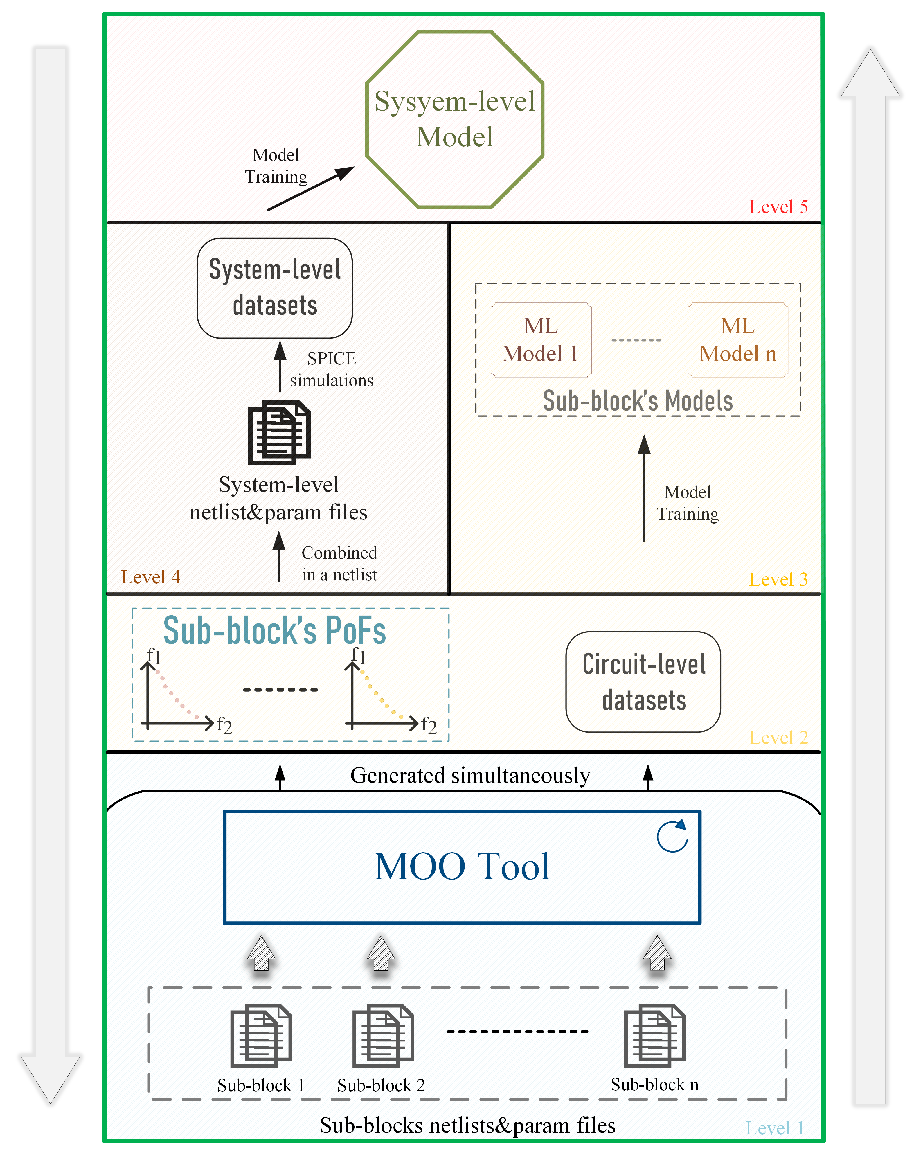
Figure 2.
Representation of an ANN structure.
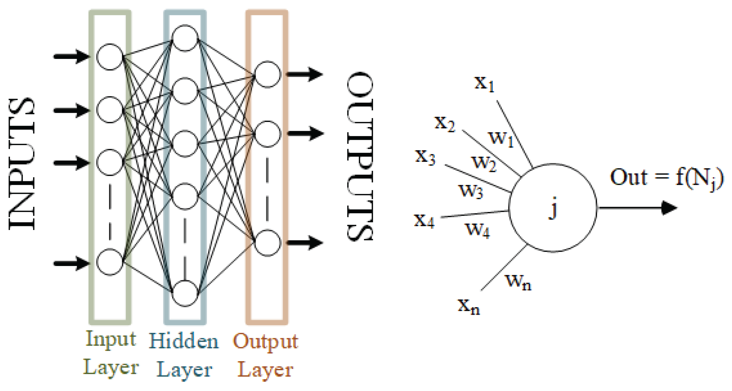
Figure 3.
Proposed hierarchical synthesis approach.
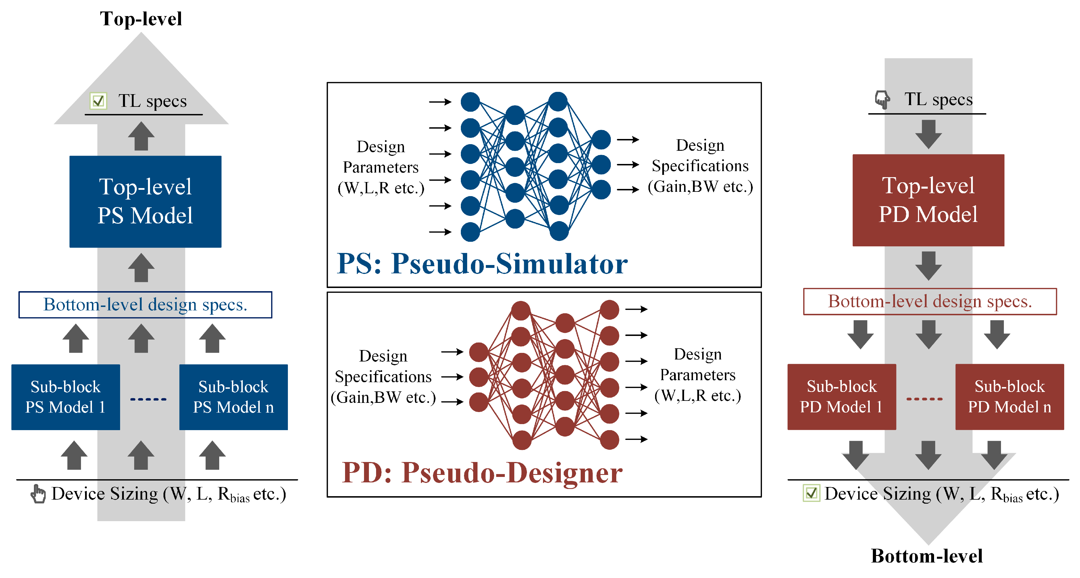
Figure 4.
Blocking schema of the flash ADC.
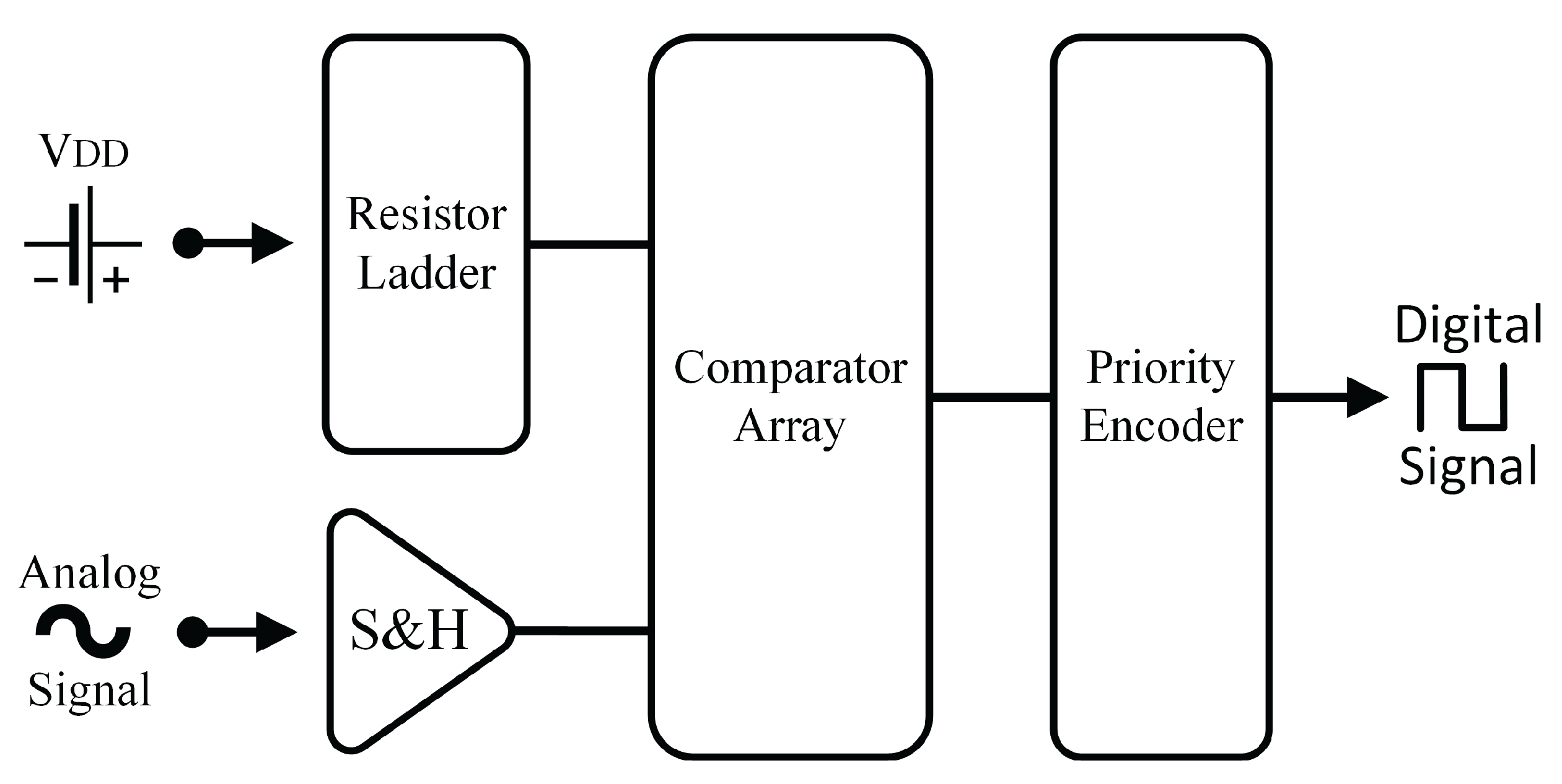
Figure 5.
Sample and hold circuit.
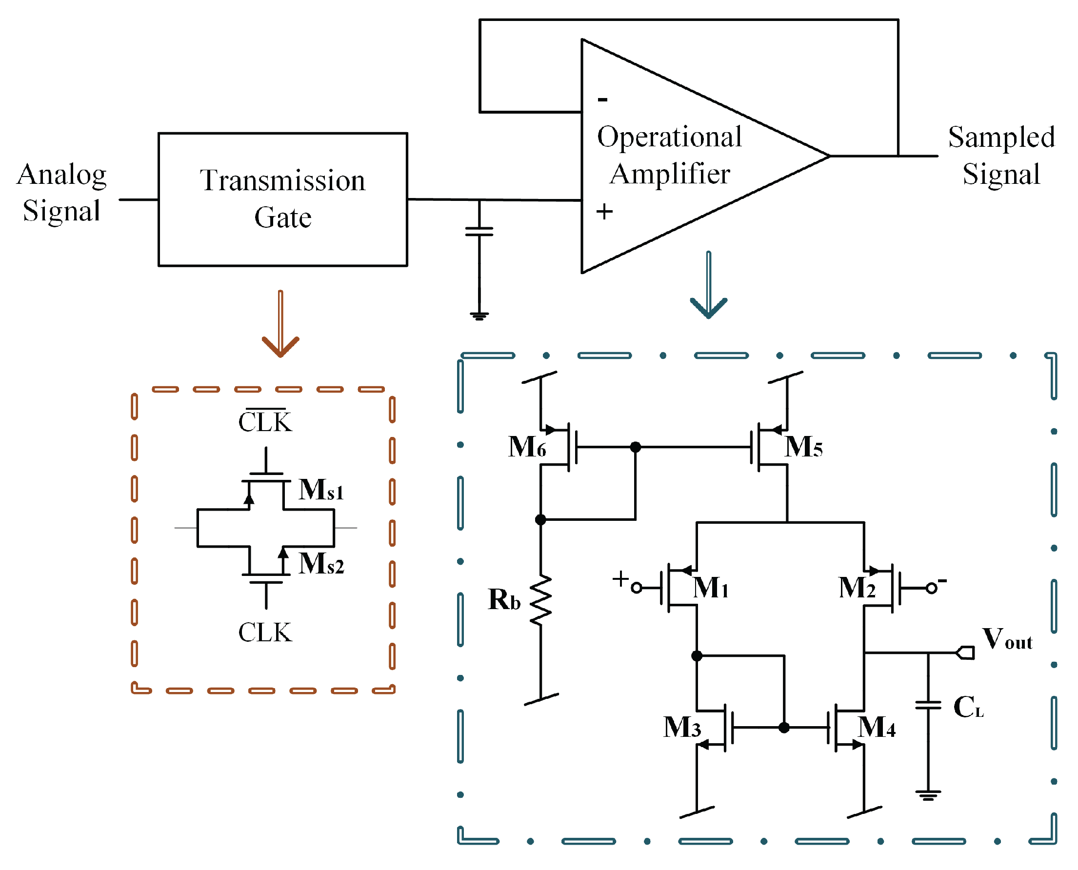
Figure 6.
Obtained PoF of differential amplifier.
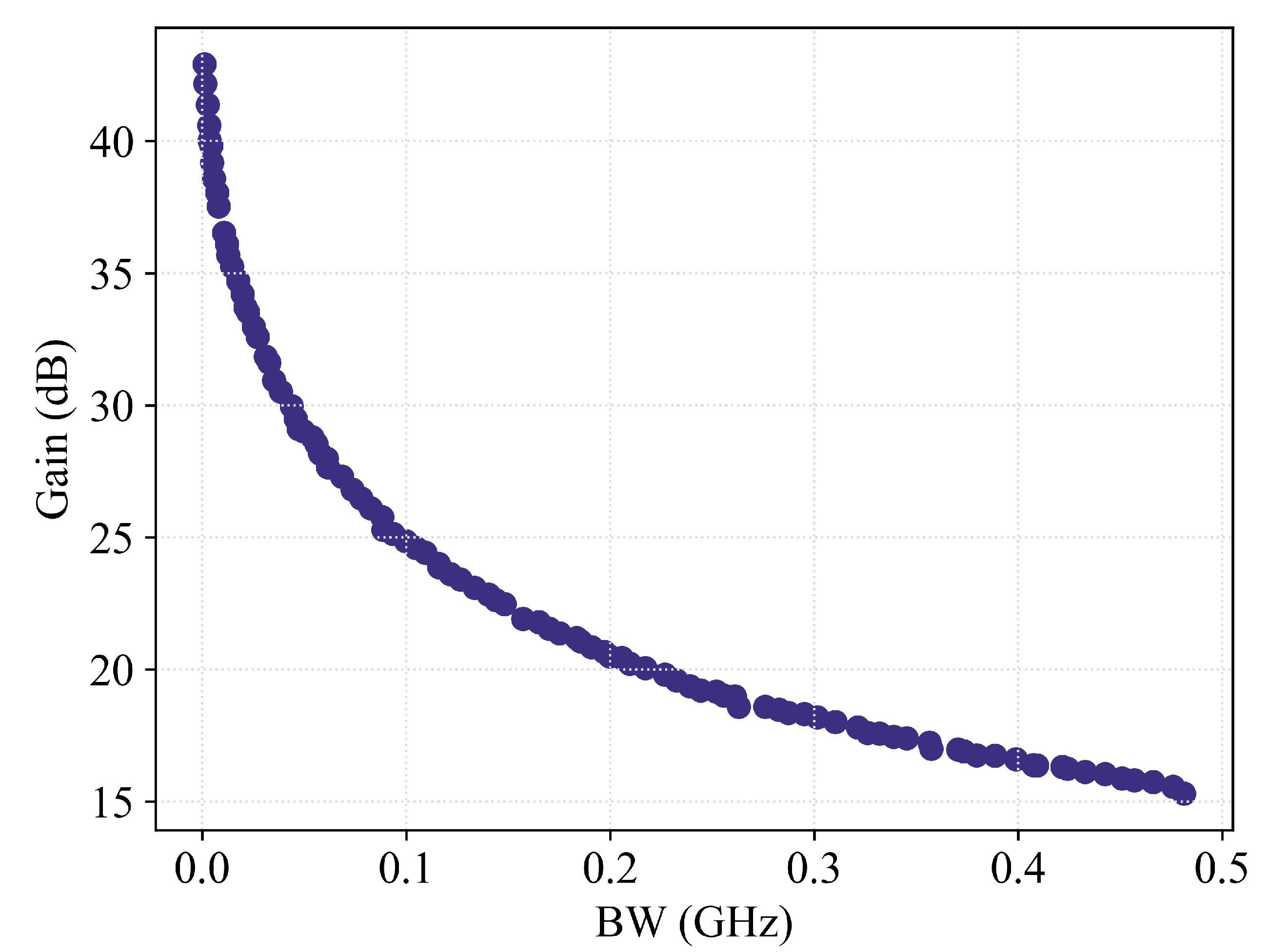
Figure 7.
Resistor ladder, comparator array, the comparator schematic.
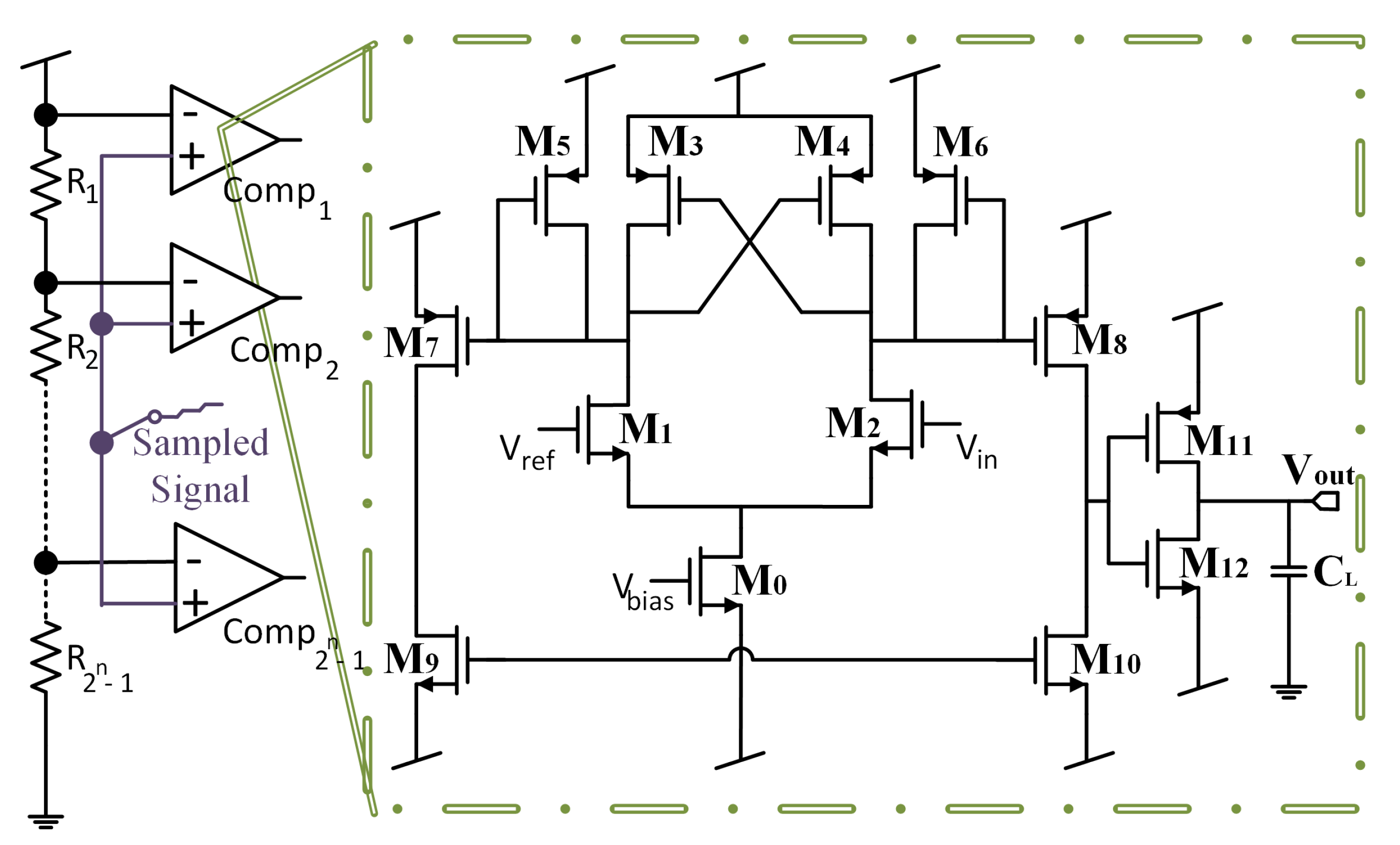
Figure 8.
Obtained PoF of voltage comparator.
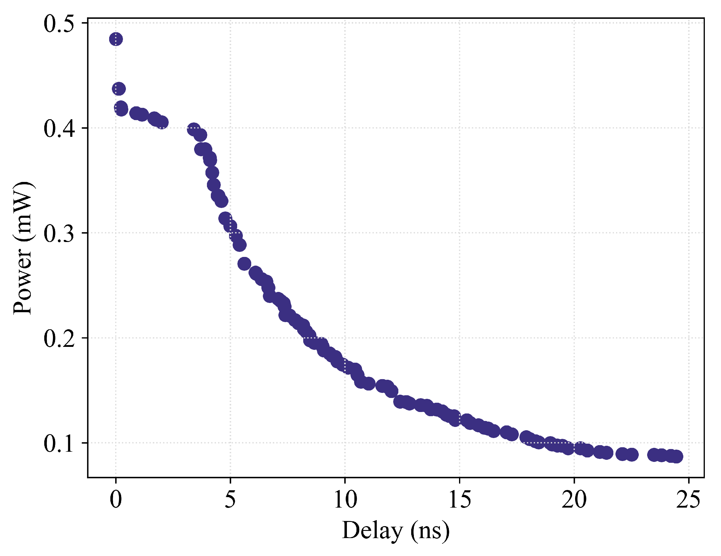
Figure 9.
Cross-product for creating system-level dataset.
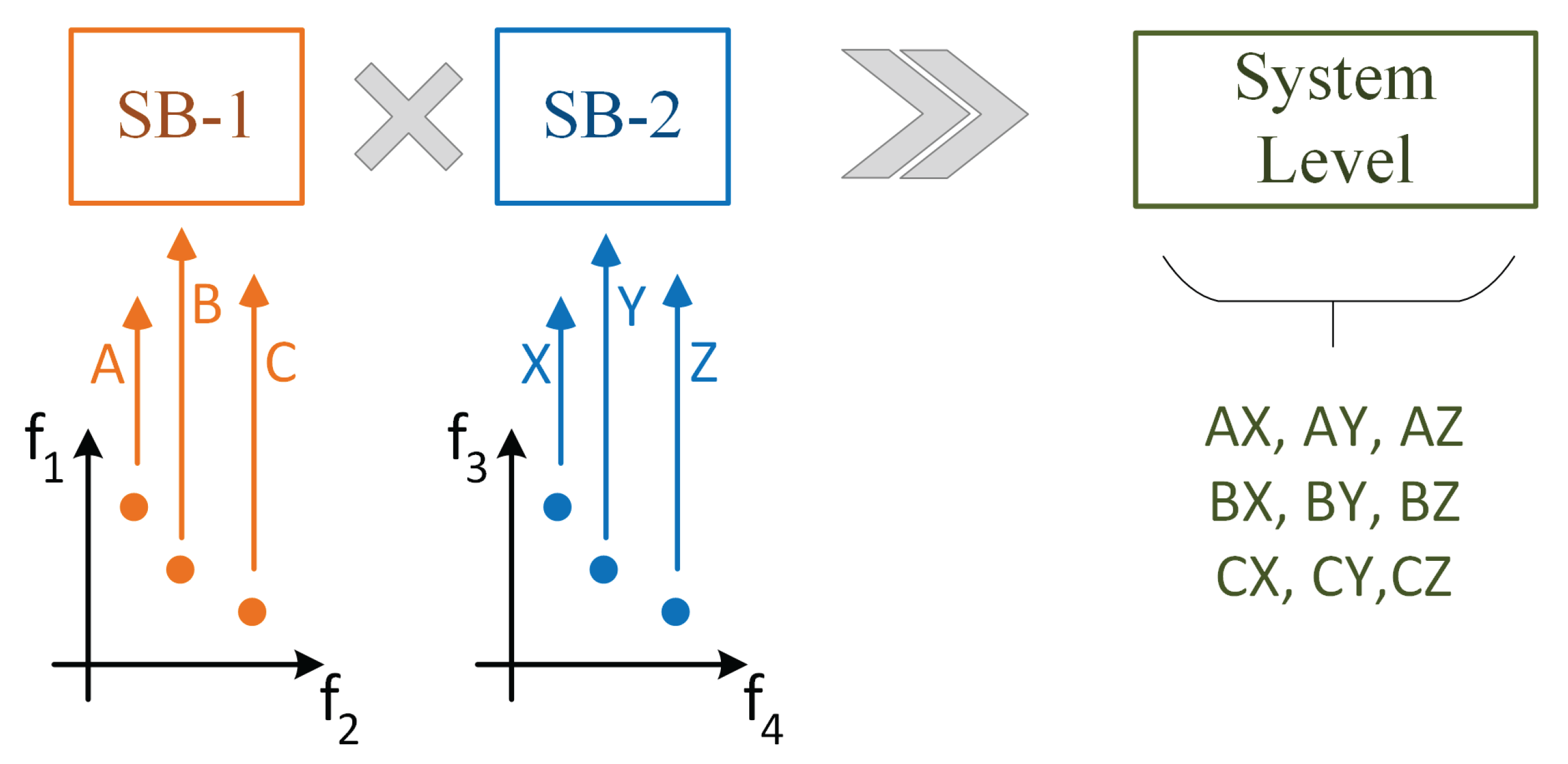
Figure 10.
Blocking Schema of the RF receiver.
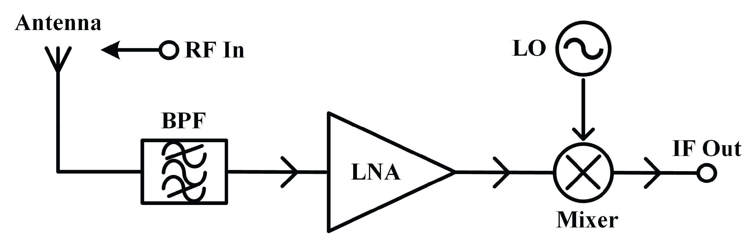
Figure 11.
Layout representations and corresponding equivalent circuit models of the MIM-capacitor and the planar inductor [29].
Figure 11.
Layout representations and corresponding equivalent circuit models of the MIM-capacitor and the planar inductor [29].
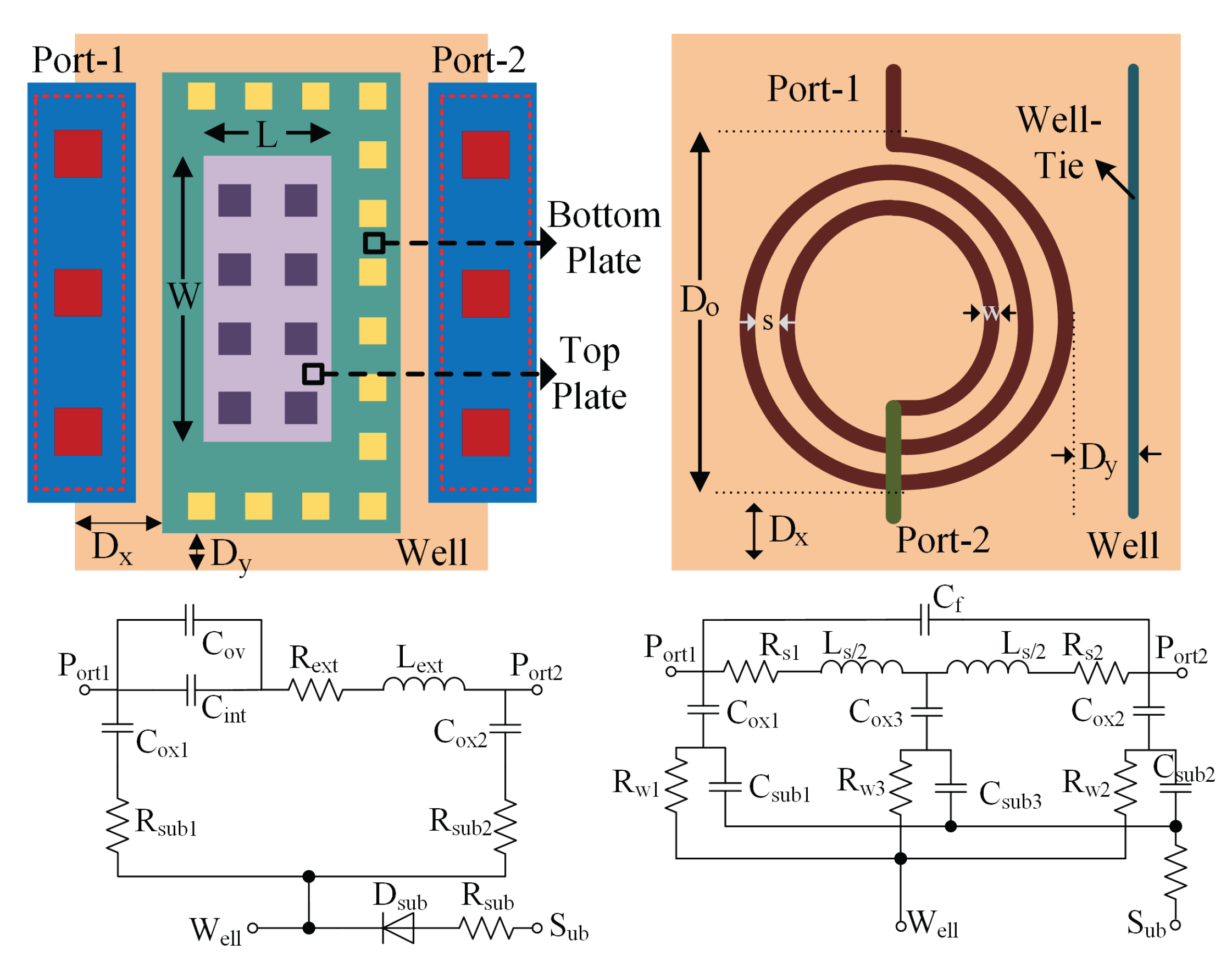
Figure 12.
LNA schematic.
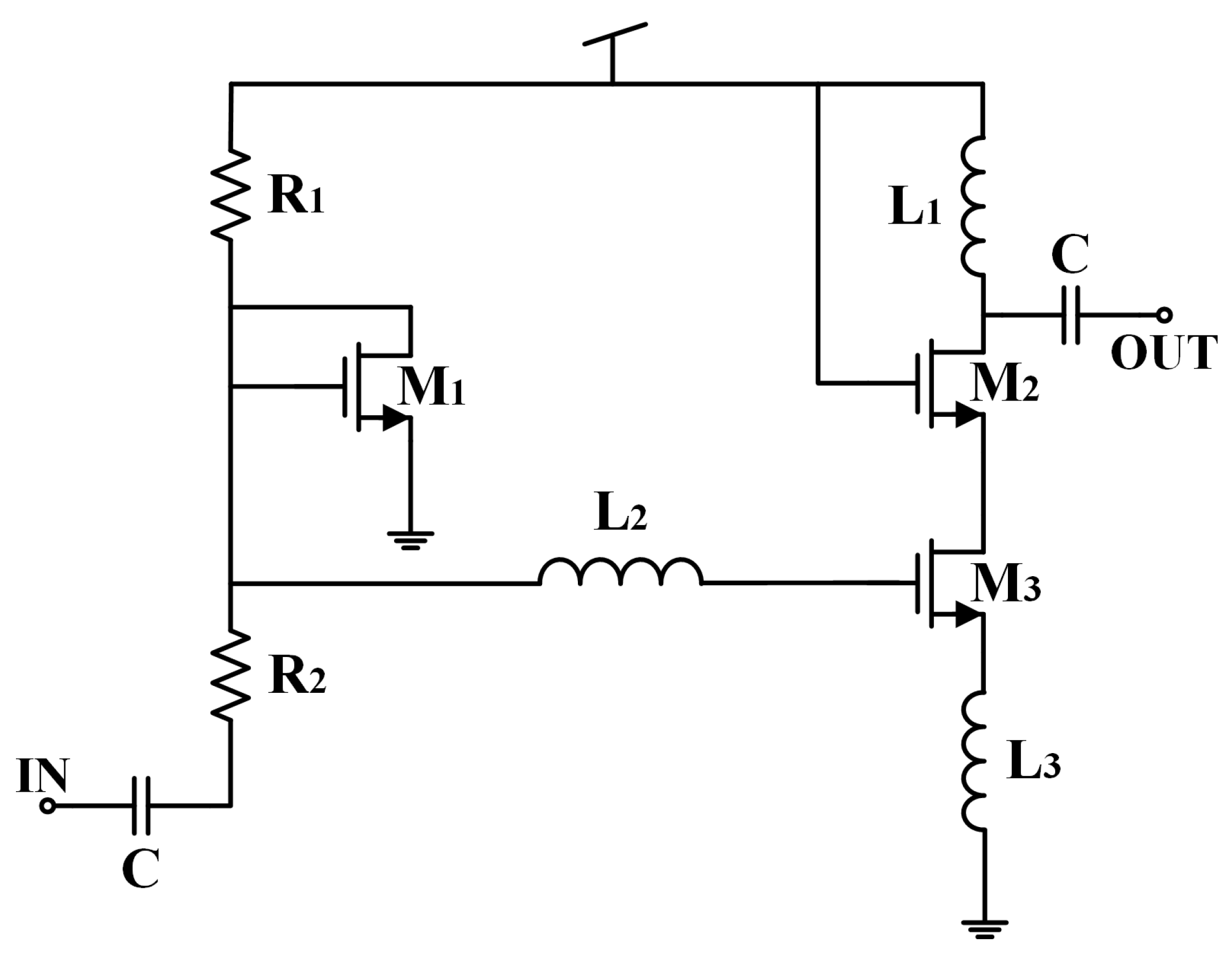
Figure 13.
Obtained PoF of the LNA circuit.
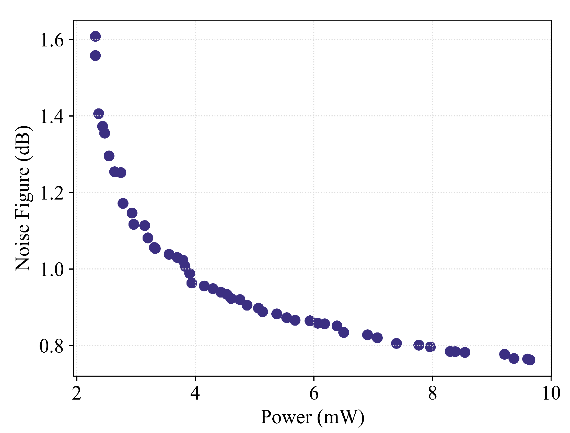
Figure 14.
Oscillator schematic.
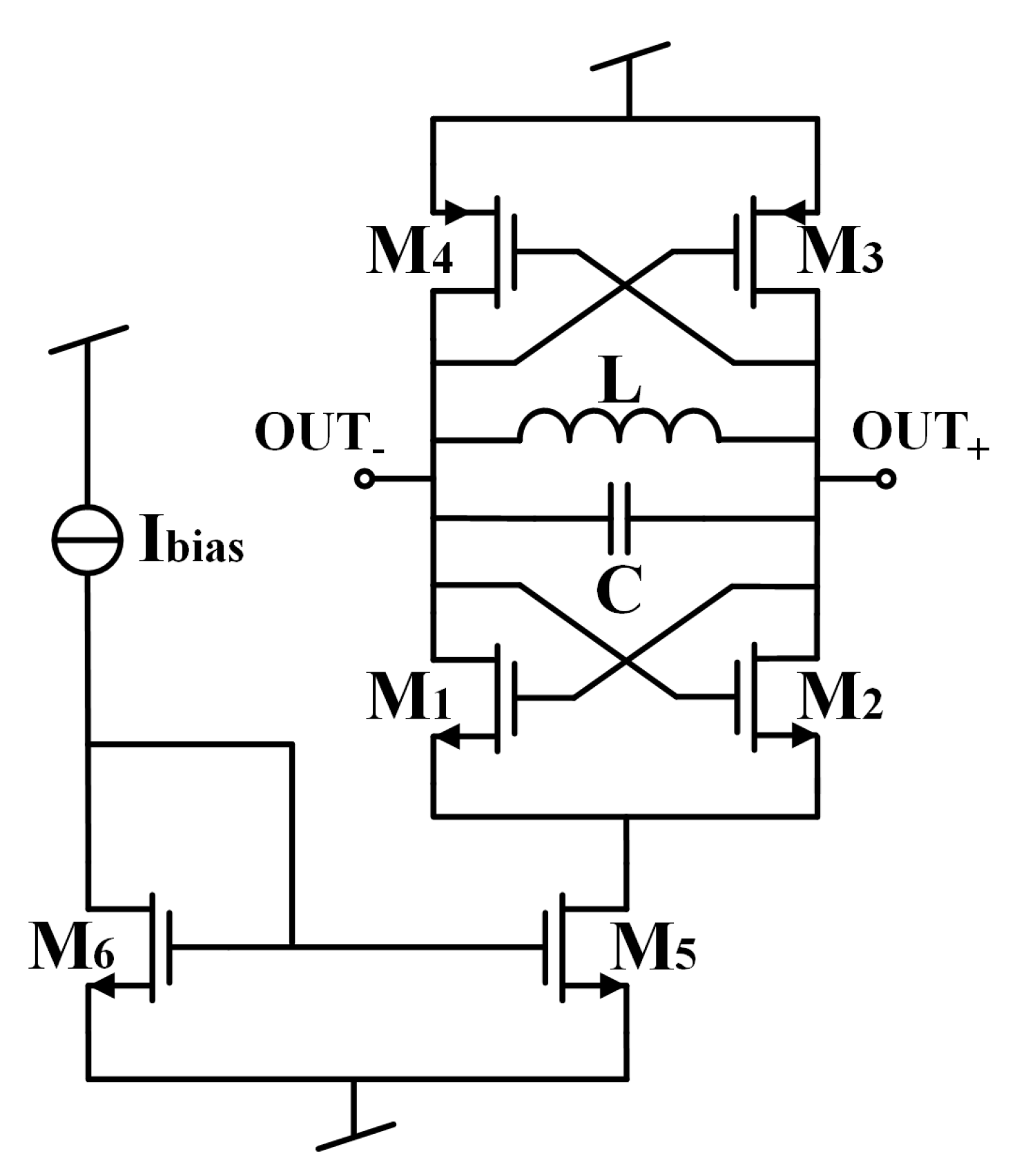
Figure 15.
Obtained PoF of the oscillator.
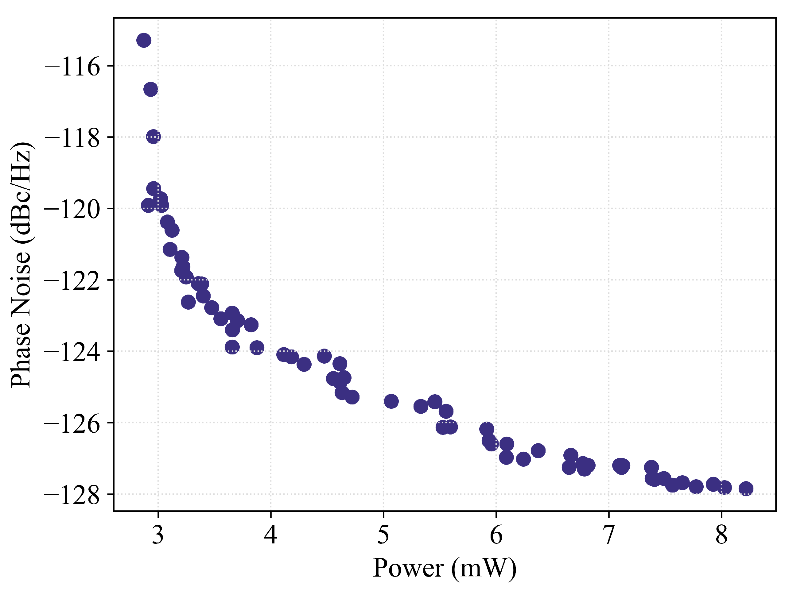
Figure 16.
Mixer schematic.
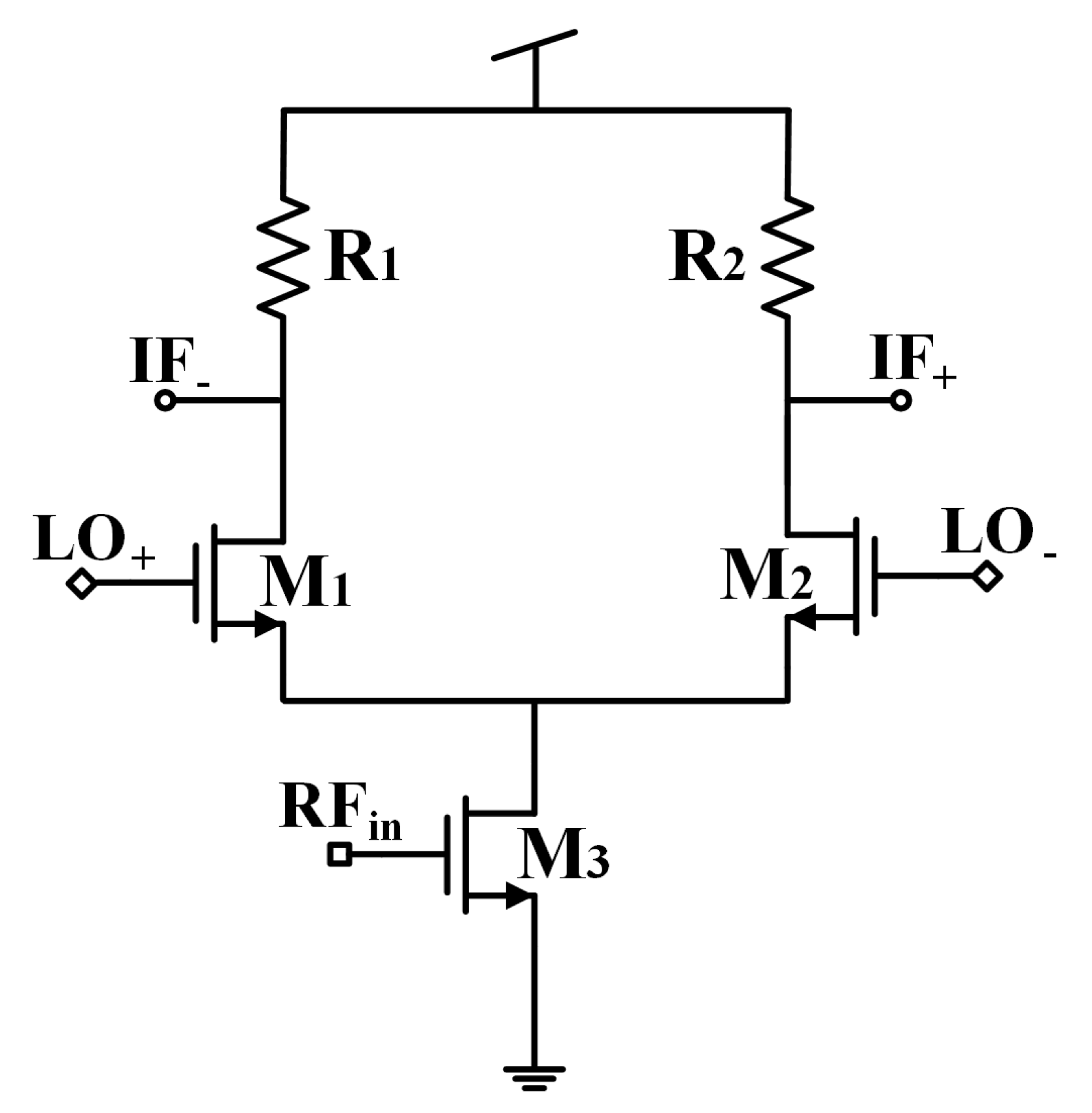
Figure 17.
Obtained PoF of the mixer.
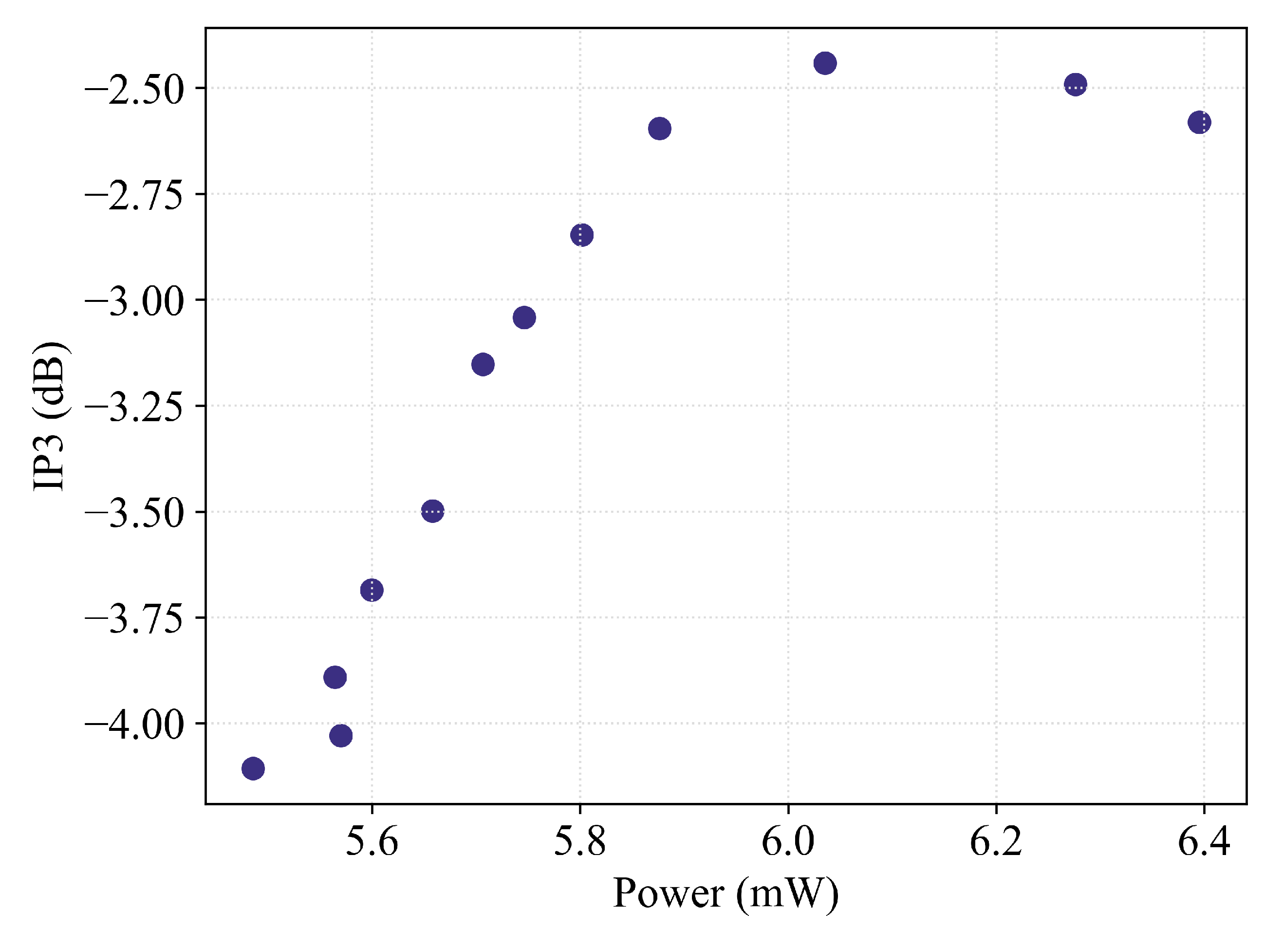
Figure 18.
Test methodology for the proposed approach.
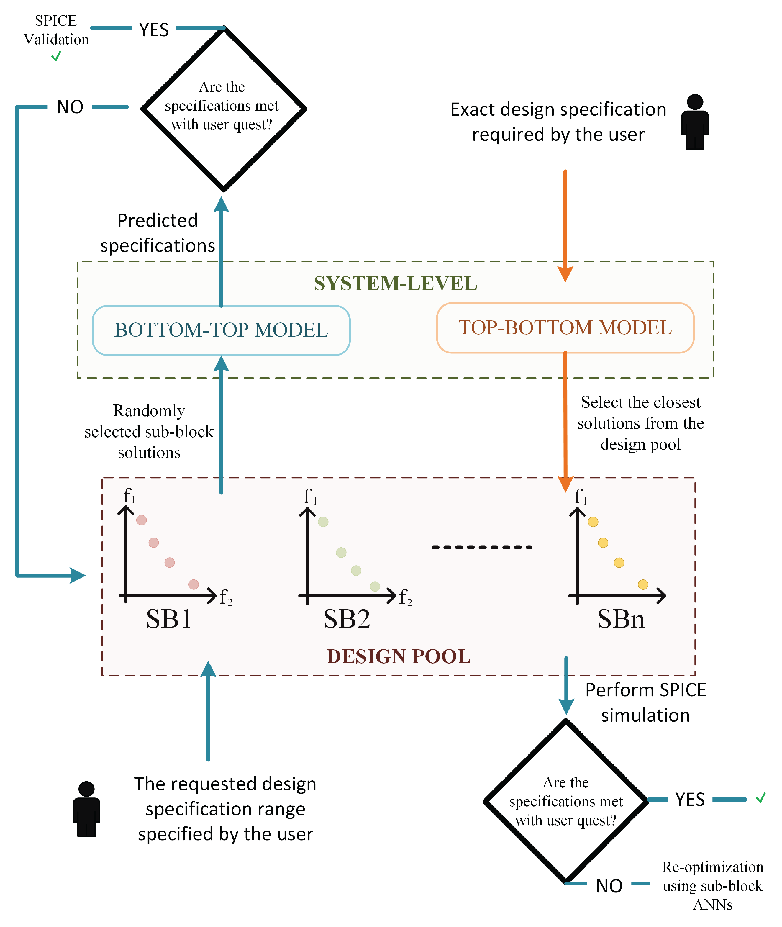
Figure 19.
Transient response of a selected ADC design obtained from synthesis.
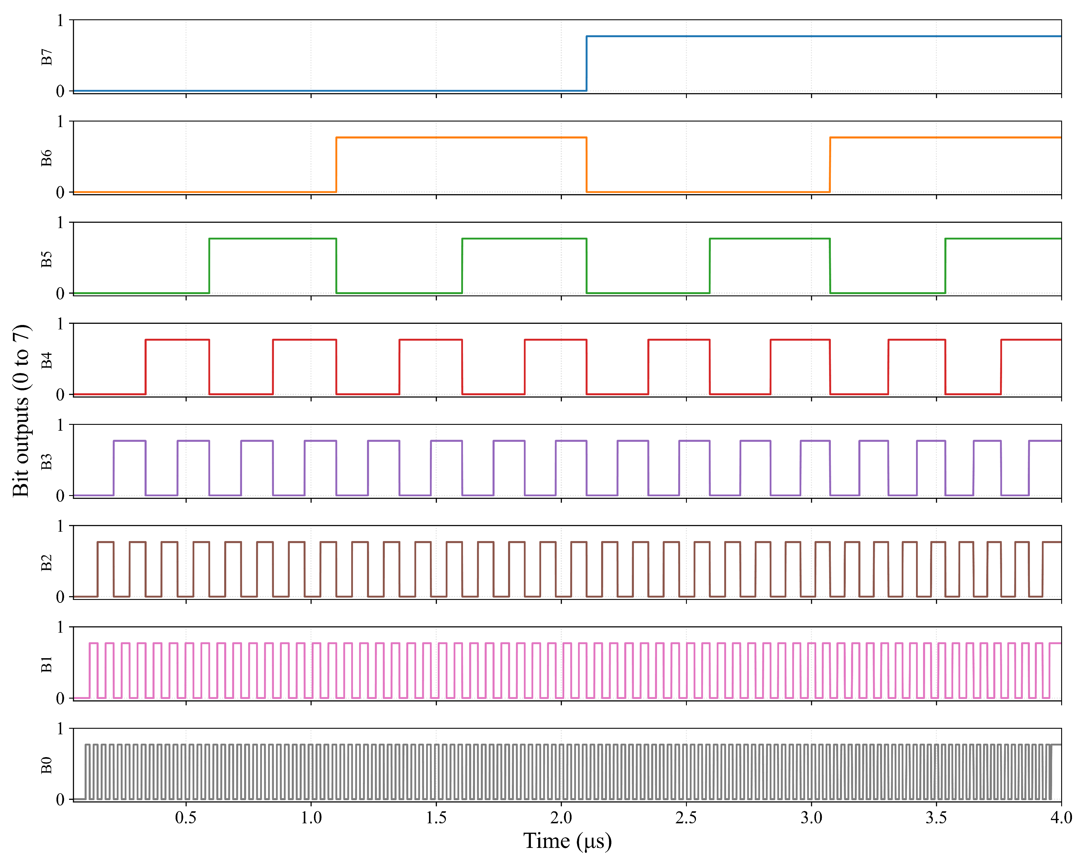
Figure 20.
Ideal ADC output vs designed ADC output.
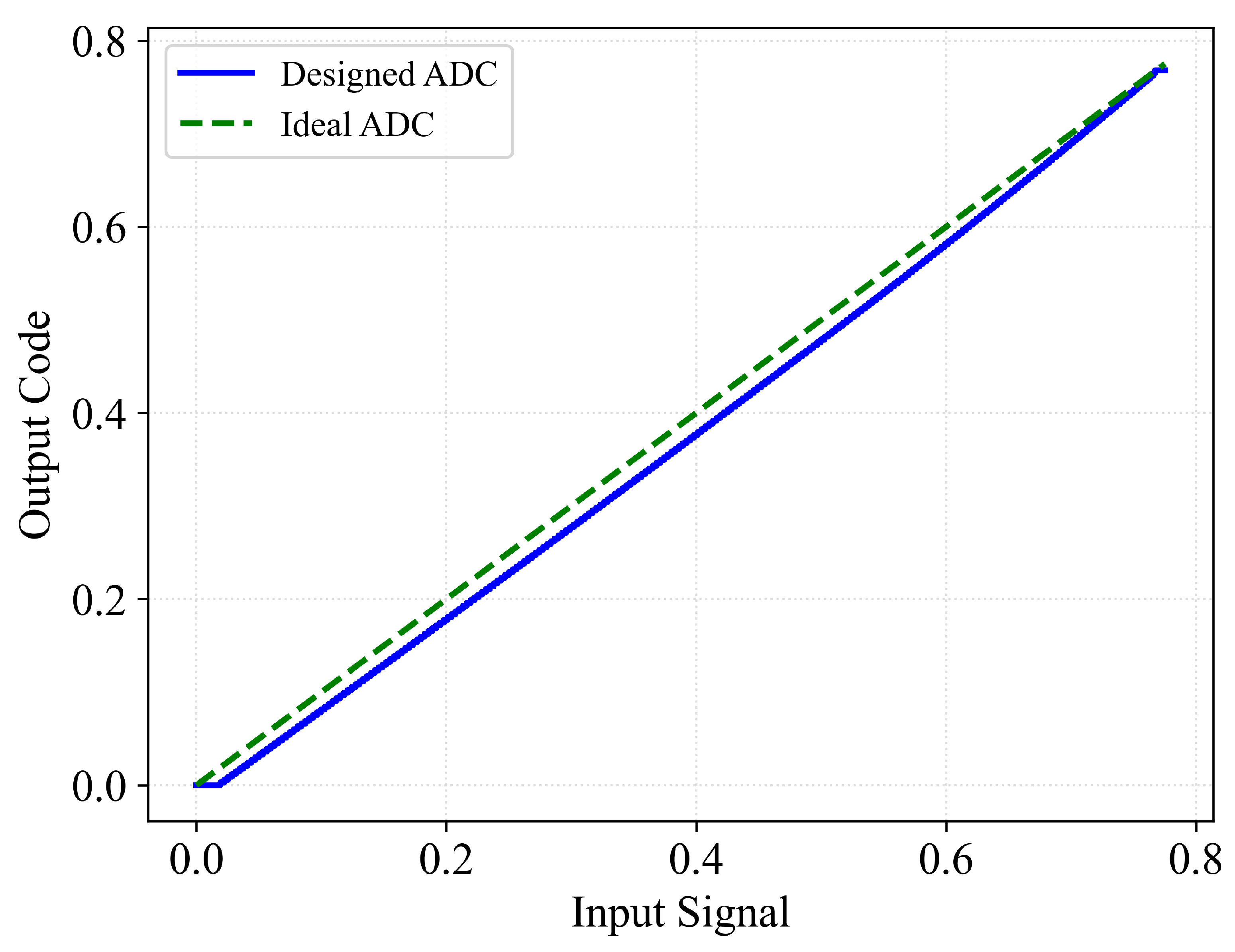
Figure 21.
Transient simulation plots of the selected receiver design.
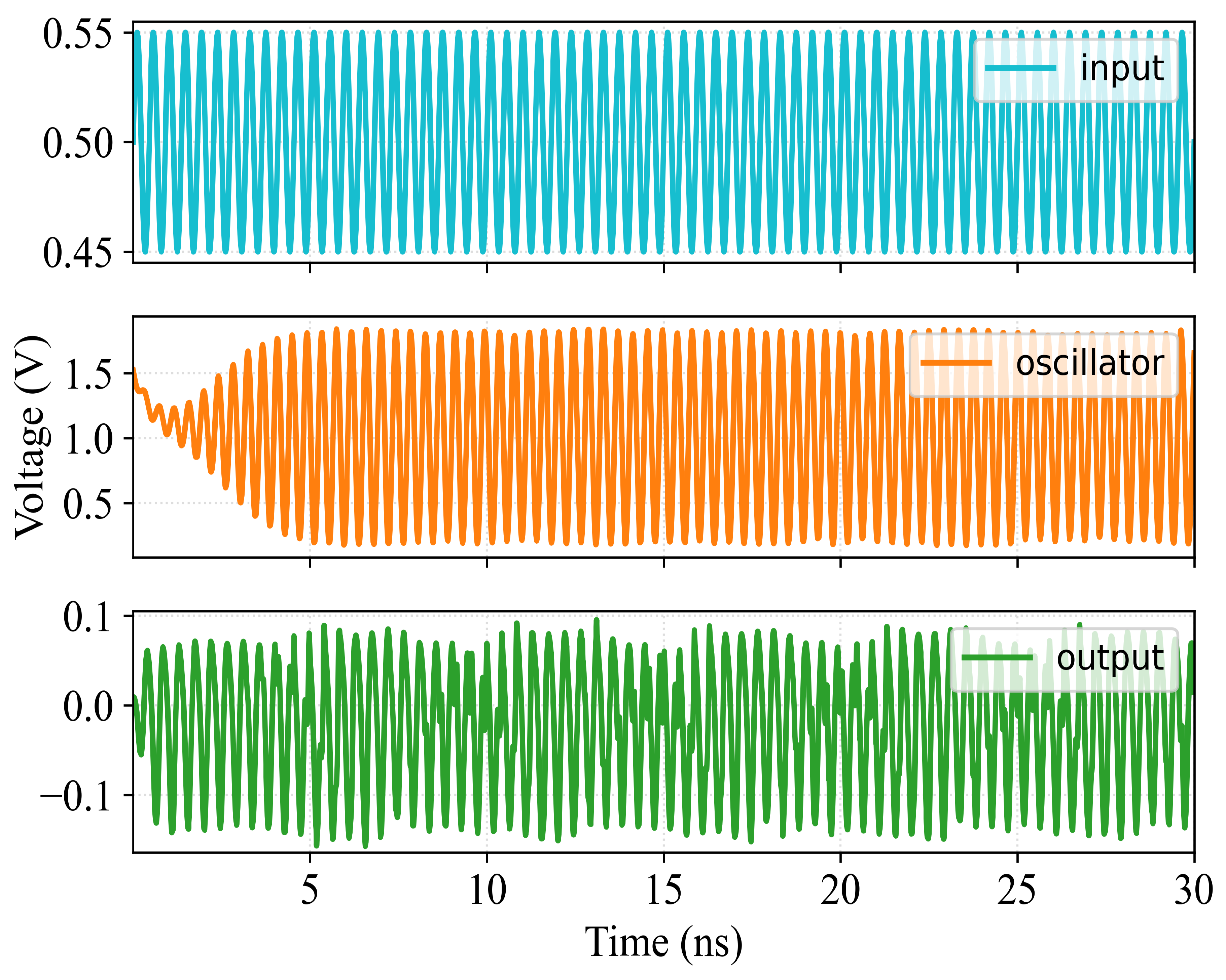
Figure 22.
FFT plots of selected receiver design: (a)Input voltage. (b) Output voltage. (c) Input power. (d) Output power.
Figure 22.
FFT plots of selected receiver design: (a)Input voltage. (b) Output voltage. (c) Input power. (d) Output power.
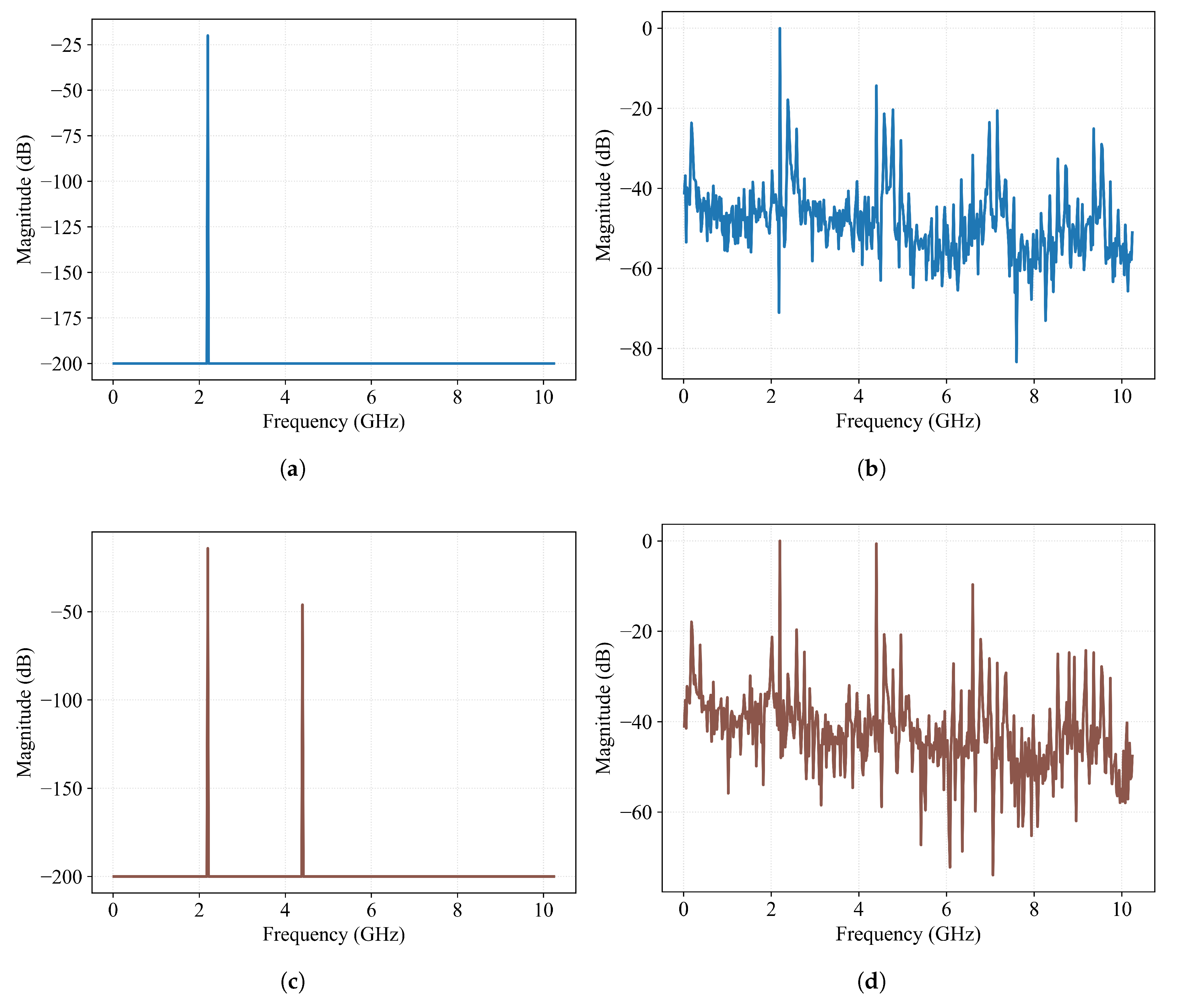

Table 1.
Optimization and modeling parameters of differential amplifier.
| Optimization | Modeling | |||||||||
|---|---|---|---|---|---|---|---|---|---|---|
| Parameters | Objectives and Constraints | Pseudo-Simulator | Pseudo-Designer | |||||||
| [m] | [] | Gain (max.) | BW (max.) | Power | PM | INPUTS (7): | INPUTS (4): Gain, BW, PM, Power | |||
| min | 0.13, 0.65 | 100 | – | OUTPUTS (4): Gain, BW, PM, Power | OUTPUTS (7): | |||||
| max | 1.3, 97.5 | 10k | – | – | – | – | NN Model: ReLU(64)-ReLU(128) | NN Model: ReLU(64)-ReLU(128) | ||
* BW: Bandwidth (unity gain), PM: Phase margin.
Table 2.
Optimization and modeling parameters of voltage comparator.
| Optimization | Modeling | |||||||
|---|---|---|---|---|---|---|---|---|
| Parameters | Objectives and Constraints | Pseudo-Simulator | Pesudo-Designer | |||||
| L [m] | W [m] | Power(min.) | Delay(min.) | INPUTS (5): | INPUTS (2): Power, Delay | |||
| min | 0.13 | 1 | mW | s | OUTPUTS (2): Power, Delay | OUTPUTS (5): | ||
| max | 1.3 | 80 | NN Model: ReLU(64)-ReLU(128) | NN Model: ReLU(64)-ReLU(128) | ||||
Table 3.
Summary of system-level modeling of 8-bit ADC.
| Pseudo-Simulator | Pseudo-Designer | |
|---|---|---|
| Input | , , , , | Best fitted INL, DNL |
| Output | Best fitted INL, DNL | , , , , |
| NN Model | ReLU(64)-D.O(30%)-ReLU(64)-D.O(30%)-ReLU(64)-D.O(30%) | ReLU(64)-D.O(30%)-ReLU(64)-D.O(30%)-ReLU(128)-D.O(30%) |
| Time, MSE | Dataset Generation & Training: 30.5 hours, 0.01 | Dataset Generation & Training: 30.5 hours, 0.005 |
* D.O: Drop-out layer.
Table 4.
Optimization and modeling parameters of LNA.
| Design Parameters | ||||||
|---|---|---|---|---|---|---|
| min | 0.13, 24 | 1k | 75 | 2 | 2.5 | 1.5 |
| max | 1, 480 | 15k | 150 | 10 | 7.5 | 2.5 |
|
Obj.& Const. |
NF (min.) | Power (min.) | Freq. | |||
| – | ||||||
| Modeling | ||||||
|
Pseudo Simulator |
IN - ReLU(128) - ReLU(128) - OUT; IN (20): Design Parameters – OUT (5): S-params, Power, Noise Figure |
|||||
|
Pseudo Designer |
IN - ReLU(360) - D.O - ReLU(260) - D.O - ReLU(512) - D.O - OUT; IN (5): S-params, Power, Noise Figure – OUT (20): Design Parameters |
|||||
* NF: Noise Figure; all S-parameters are in dB; D.O: Drop-out layer with 50% rate.
Table 5.
Design parameters of oscillator.
| min | 0.13 | 10, 10 | 0.5 | 10, 10 | 135 | 3 | 5 | 1.5 |
| max | 1 | 35, 500 | 6 | 30, 35 | 150 | 5.5 | 7.5 | 2.5 |
* Wc.c: Width of the cross-coupled transistors; Wb.c: Width of the bias current transistors; Ib: Bias current.
Table 6.
Optimization and modeling parameters of oscillator.
| Objectives & Constraints | Modeling | |||
|---|---|---|---|---|
| Phase Noise @1 MHz(min.) | -150 <PN [dBc/Hz] <-115 |
Pseudo Simulator |
IN - ReLU(64) - ReLU(64) - OUT; | |
| Power Consumption(min.) | <10 mW | IN (13): Design parameters – OUT (4): PN, power, signal amplitude, frequency | ||
| Oscillation Frequency | 2.39 < [GHz] <2.41 |
Pseudo Designer |
IN - ReLU(64) - ReLU(128) - OUT; | |
| Signal Amplitude @(3&7)ns | >1V | IN (4): PN, power, signal amplitude, frequency – OUT (13): Design parameters | ||
Table 7.
Optimization and modeling parameters of mixer.
| Optimization | Modeling | ||||||||
|---|---|---|---|---|---|---|---|---|---|
| Parameters | Objectives & Constraints | Pseudo-Simulator | Pseudo-Designer | ||||||
| Power (min.) | IP3 (max.) | CG | IN (5): ; OUT (3): Power, IP3, CG | IN (3): Power, IP3, CG; OUT (5): | |||||
| min | 0.13, 1 | 50 | mW | dB | dB | IN - ReLU(64) - ReLU(64) - OUT | IN - ReLU(360) - D.O. (50%) - ReLU(260) - D.O. (50%) - ReLU(512) - D.O. (50%) - OUT |
||
| max | 4, 500 | 300k | |||||||
* CG: Conversion gain; IP3: Third-order intercept point.
Table 8.
Summary of system-level modeling of heterodyne receiver.
| Pseudo-Simulator | Pseudo-Designer | |
|---|---|---|
| Input | Conversion Gain, IP3 | |
| Output | Conversion Gain, IP3 | |
| NN Model | ReLU-ReLU-DO(45%)-ReLU-ReLU-DO(25%)-ReLU-ReLU | ReLU-ReLU-DO(45%)-ReLU-ReLU-ReLU-ReLU |
| Time, MSE | Dataset Generation & Training: 32 hours, 0.124 | Dataset Generation & Training: 32 hours, 0.06 |
* All hidden layers activated by Rectified Linear Unit (ReLU) function with 360 neurons.
Table 9.
Synhtesis result of ADC with top-to-bottom modeling approach.
| Requested DNL (LSB) |
Requested INL (LSB) |
Requested Word Count |
Obtained DNL (Syhtnesis) |
Obtained INL (Syhtnesis) |
Obtained Word Count (Syhtnesis) |
Error DNL (LSB) % |
Error INL (LSB) % |
Synthesis Time (ms) |
|---|---|---|---|---|---|---|---|---|
| 0.166 | 0.0653 | 256 | 0.166 | 0.0648 | 256 | 0 | 0.76 | 890 |
| 0.5 | 0.0736 | 256 | 0.566 | 0.0744 | 256 | 13.2 | 1.08 | 940 |
| 0.166 | 0.0921 | 256 | 0.166 | 0.0986 | 256 | 0 | 7.05 | 890 |
| 0.2 | 0.1337 | 256 | 0.166 | 0.1338 | 256 | 17 | 0.07 | 990 |
| 0.166 | 0.1494 | 256 | 0.166 | 0.1522 | 256 | 0 | 1.87 | 830 |
* INL was calculated using best straight line method.
Table 10.
Synthesis results of ADC with bottom-to-top modeling approach.
| Design Specifications | Model Results | ||||||
|---|---|---|---|---|---|---|---|
| DNL (LSB) | INL (LSB) | Word Count | DNL (LSB) | INL (LSB) | Word Count | ||
| <0.5 | <0.5 | 256 | 0.166 | 0.24 | 256 | ||
| <0.5 | <0.5 | 256 | 0.133 | 0.445 | 256 | ||
| <0.5 | <0.5 | 256 | 0.233 | 0.508 | 256 | ||
| <0.5 | <0.5 | 256 | 0.233 | 0.364 | 256 | ||
| <0.5 | <0.5 | 256 | 0.166 | 0.149 | 256 | ||
Table 11.
Synthesis results of the receiver for both modeling approaches.
| Top-to-bottom | Bottom-to-top | ||||||||
|---|---|---|---|---|---|---|---|---|---|
|
Requested CG (dB) |
Requested IP3 (dB) |
Obtained CG (Syhtnesis) |
Obtained IP3 (Syhtnesis) |
Error CG (dB) % |
Error IP3 (dB) % |
Synthesis Time (ms) |
CG (dB) >-10 |
IP3 (dB) >-10 |
|
| -9.34 | -5.76 | -9.61 | -6.31 | 2.89 | 9.54 | 770 | -5.47 | -6.13 | |
| -8.38 | -5.9 | -8.4 | -6.06 | 0.23 | 2.71 | 850 | -5.59 | -6.15 | |
| -9.34 | -5.8 | -9.29 | -5.9 | 0.53 | 1.72 | 980 | -5.72 | -6.07 | |
| -12.62 | -3.55 | -12.65 | -3.97 | 0.23 | 11.83 | 730 | -5.8 | -6.98 | |
| -10.34 | -5.76 | -10.81 | -6.16 | 4.54 | 6.94 | 940 | -6.52 | -8.28 | |
Table 12.
Comparison of the prior work on hierarchical circuit automation.
| [42] | [44] | [45] | [46] | This Work | |
|---|---|---|---|---|---|
|
Circuit Complexity |
Three-stage OPAMP & active filter topologies |
SAR ADC | RF front-end receiver | W-Band front-end receiver |
Full-flash ADC & RF front-end receiver |
|
Synthesis Direction |
Top-to-bottom | Top-to-bottom | Bottom-to-top | Bottom-to-top | Both direction |
|
Automation Method |
Tool firstly decides propoer sub-circuit. As following step NN classfier determine tran- sistor level topology. Finally, tool sizes all-sub-circuits via local and global optimization, which are carried out by PSO and NN, respectively. |
Top level specs are mapped to components via design equa- tions. Digital part uses redun- dancy optimizaiton, while ana- log relies on Bayesian optimi- zation. Layouts of the analog part generated automatically. |
Firstly, PoFs are generated for inductor using surrogate mo- dels. As a second step, subcir- cuits are synhtesized, where in- ductors are selected from exis- ting PoFs via matrix mapping technique. The same flow conti- nues to acheive top-level. |
Component libraries are pre- pared to utilize in an optimiza- tion loop. These libraries faci- litate the RF sub-block synthe- sis without compromising accu- racy. Pre-existed PoFs of the sub-blocks are used to achieve high-level synthesis. |
All system sub-blocks are synt- hesized while generating corres- ponding circuit dataset. Each sub-block is modeled bi-directi- onally. At the system level, cir- cuits are only represented by design specifications, and ANN models handle synthesis both directions. |
|
Used Algorithms |
NN classifier/regressor, PSO |
Design equations, redundancy optimization, BO |
Surrogate Model, EA | EA | ANN, EA |
| Accuracy | for OPAMP 94.1% & for filter 94.6% |
User intervention may be required in the synthesis. |
Approximately 99% | Not specified | **Receiver Model: 95.89% & *ADC Model: 95.9% |
| Speed | OPAMP: 9.4 h & filter: Not specified |
2 h | 27 h | 16.5 days | *BT for receiver: 35.5 h & for ADC: 34 h TB for receiver: 35 h & for ADC: 31 h |
|
Key Propoerty |
Dataset expansion via NN reduces training time. |
ADC layouts are generated based on user requests |
Stored PoFs can be reused for any circuit operating in the same band. |
Different topologies can be efficiently synthesized using the libraries. |
Sub-block models enable rapid synthesis even for out-of-space design requests. |
* BT: Bottom-to-top modeling approach; TB: Top-to-bottom modeling approach. The synthesis times include both the training and dataset creation phases. After the model is trained, synthesis takes less than a second. ** Average accuracy for the five independent top-to-bottom syntheses, where SPICE simulations serve as a performance benchmark.
Disclaimer/Publisher’s Note: The statements, opinions and data contained in all publications are solely those of the individual author(s) and contributor(s) and not of MDPI and/or the editor(s). MDPI and/or the editor(s) disclaim responsibility for any injury to people or property resulting from any ideas, methods, instructions or products referred to in the content. |
© 2025 by the authors. Licensee MDPI, Basel, Switzerland. This article is an open access article distributed under the terms and conditions of the Creative Commons Attribution (CC BY) license (http://creativecommons.org/licenses/by/4.0/).
Copyright: This open access article is published under a Creative Commons CC BY 4.0 license, which permit the free download, distribution, and reuse, provided that the author and preprint are cited in any reuse.


